WO2025027677A1 - 超硬合金および切削工具 - Google Patents
超硬合金および切削工具 Download PDFInfo
- Publication number
- WO2025027677A1 WO2025027677A1 PCT/JP2023/027732 JP2023027732W WO2025027677A1 WO 2025027677 A1 WO2025027677 A1 WO 2025027677A1 JP 2023027732 W JP2023027732 W JP 2023027732W WO 2025027677 A1 WO2025027677 A1 WO 2025027677A1
- Authority
- WO
- WIPO (PCT)
- Prior art keywords
- cemented carbide
- intensity
- less
- peak
- tungsten
- Prior art date
- Legal status (The legal status is an assumption and is not a legal conclusion. Google has not performed a legal analysis and makes no representation as to the accuracy of the status listed.)
- Pending
Links
Images


Classifications
-
- B—PERFORMING OPERATIONS; TRANSPORTING
- B23—MACHINE TOOLS; METAL-WORKING NOT OTHERWISE PROVIDED FOR
- B23B—TURNING; BORING
- B23B27/00—Tools for turning or boring machines; Tools of a similar kind in general; Accessories therefor
- B23B27/14—Cutting tools of which the bits or tips or cutting inserts are of special material
- B23B27/148—Composition of the cutting inserts
-
- C—CHEMISTRY; METALLURGY
- C22—METALLURGY; FERROUS OR NON-FERROUS ALLOYS; TREATMENT OF ALLOYS OR NON-FERROUS METALS
- C22C—ALLOYS
- C22C1/00—Making non-ferrous alloys
- C22C1/04—Making non-ferrous alloys by powder metallurgy
- C22C1/05—Mixtures of metal powder with non-metallic powder
- C22C1/051—Making hard metals based on borides, carbides, nitrides, oxides or silicides; Preparation of the powder mixture used as the starting material therefor
-
- C—CHEMISTRY; METALLURGY
- C22—METALLURGY; FERROUS OR NON-FERROUS ALLOYS; TREATMENT OF ALLOYS OR NON-FERROUS METALS
- C22C—ALLOYS
- C22C29/00—Alloys based on carbides, oxides, nitrides, borides, or silicides, e.g. cermets, or other metal compounds, e.g. oxynitrides, sulfides
- C22C29/005—Alloys based on carbides, oxides, nitrides, borides, or silicides, e.g. cermets, or other metal compounds, e.g. oxynitrides, sulfides comprising a particular metallic binder
-
- C—CHEMISTRY; METALLURGY
- C22—METALLURGY; FERROUS OR NON-FERROUS ALLOYS; TREATMENT OF ALLOYS OR NON-FERROUS METALS
- C22C—ALLOYS
- C22C29/00—Alloys based on carbides, oxides, nitrides, borides, or silicides, e.g. cermets, or other metal compounds, e.g. oxynitrides, sulfides
- C22C29/02—Alloys based on carbides, oxides, nitrides, borides, or silicides, e.g. cermets, or other metal compounds, e.g. oxynitrides, sulfides based on carbides or carbonitrides
-
- C—CHEMISTRY; METALLURGY
- C22—METALLURGY; FERROUS OR NON-FERROUS ALLOYS; TREATMENT OF ALLOYS OR NON-FERROUS METALS
- C22C—ALLOYS
- C22C29/00—Alloys based on carbides, oxides, nitrides, borides, or silicides, e.g. cermets, or other metal compounds, e.g. oxynitrides, sulfides
- C22C29/02—Alloys based on carbides, oxides, nitrides, borides, or silicides, e.g. cermets, or other metal compounds, e.g. oxynitrides, sulfides based on carbides or carbonitrides
- C22C29/06—Alloys based on carbides, oxides, nitrides, borides, or silicides, e.g. cermets, or other metal compounds, e.g. oxynitrides, sulfides based on carbides or carbonitrides based on carbides, but not containing other metal compounds
- C22C29/067—Alloys based on carbides, oxides, nitrides, borides, or silicides, e.g. cermets, or other metal compounds, e.g. oxynitrides, sulfides based on carbides or carbonitrides based on carbides, but not containing other metal compounds comprising a particular metallic binder
-
- C—CHEMISTRY; METALLURGY
- C22—METALLURGY; FERROUS OR NON-FERROUS ALLOYS; TREATMENT OF ALLOYS OR NON-FERROUS METALS
- C22C—ALLOYS
- C22C29/00—Alloys based on carbides, oxides, nitrides, borides, or silicides, e.g. cermets, or other metal compounds, e.g. oxynitrides, sulfides
- C22C29/02—Alloys based on carbides, oxides, nitrides, borides, or silicides, e.g. cermets, or other metal compounds, e.g. oxynitrides, sulfides based on carbides or carbonitrides
- C22C29/06—Alloys based on carbides, oxides, nitrides, borides, or silicides, e.g. cermets, or other metal compounds, e.g. oxynitrides, sulfides based on carbides or carbonitrides based on carbides, but not containing other metal compounds
- C22C29/08—Alloys based on carbides, oxides, nitrides, borides, or silicides, e.g. cermets, or other metal compounds, e.g. oxynitrides, sulfides based on carbides or carbonitrides based on carbides, but not containing other metal compounds based on tungsten carbide
-
- B—PERFORMING OPERATIONS; TRANSPORTING
- B22—CASTING; POWDER METALLURGY
- B22F—WORKING METALLIC POWDER; MANUFACTURE OF ARTICLES FROM METALLIC POWDER; MAKING METALLIC POWDER; APPARATUS OR DEVICES SPECIALLY ADAPTED FOR METALLIC POWDER
- B22F5/00—Manufacture of workpieces or articles from metallic powder characterised by the special shape of the product
- B22F2005/001—Cutting tools, earth boring or grinding tool other than table ware
-
- B—PERFORMING OPERATIONS; TRANSPORTING
- B23—MACHINE TOOLS; METAL-WORKING NOT OTHERWISE PROVIDED FOR
- B23B—TURNING; BORING
- B23B2222/00—Materials of tools or workpieces composed of metals, alloys or metal matrices
- B23B2222/28—Details of hard metal, i.e. cemented carbide
-
- C—CHEMISTRY; METALLURGY
- C22—METALLURGY; FERROUS OR NON-FERROUS ALLOYS; TREATMENT OF ALLOYS OR NON-FERROUS METALS
- C22C—ALLOYS
- C22C2200/00—Crystalline structure
Definitions
- This disclosure relates to cemented carbide and cutting tools.
- cemented carbide alloys containing tungsten carbide (WC) particles and a binder phase mainly composed of cobalt, etc. have been used as materials for cutting tools (Patent Documents 1 and 2).
- the cemented carbide of the present disclosure is A cemented carbide comprising a plurality of tungsten carbide particles and a binder phase,
- the cemented carbide contains 80 volume % or more of the tungsten carbide particles and the binder phase in total,
- the cemented carbide contains the binder phase in an amount of 0.1% by volume or more and 20% by volume or less,
- the cemented carbide contains at least one first element selected from the group consisting of titanium, tantalum, niobium, zirconium, cerium, yttrium, and boron;
- the cemented carbide contains the first element in a total amount of 0.01 atomic % or more and 20 atomic % or less,
- the binder phase contains 50% by mass or more of cobalt,
- a first graph showing the results of line analysis performed using an energy dispersive X-ray spectrometer attached to a transmission electron microscope along a first direction from adjacent binder phases toward the tungsten carbide particles, the results being plotted on
- FIG. 1 is a schematic cross-sectional view of a cemented carbide according to a first embodiment.
- FIG. 2 shows an example of a first graph of the cemented carbide according to the first embodiment.
- FIG. 3 is a schematic diagram of a cutting tool according to a second embodiment.
- the present disclosure therefore aims to provide a cemented carbide that, when used as a tool material, can provide a cutting tool with a long tool life, particularly in high-speed machining of difficult-to-cut materials, as well as a cutting tool with a long tool life.
- the cemented carbide of the present disclosure is A cemented carbide comprising a plurality of tungsten carbide particles and a binder phase, The cemented carbide contains 80 volume % or more of the tungsten carbide particles and the binder phase in total, The cemented carbide contains the binder phase in an amount of 0.1% by volume or more and 20% by volume or less, The cemented carbide contains at least one first element selected from the group consisting of titanium, tantalum, niobium, zirconium, cerium, yttrium, and boron; The cemented carbide contains the first element in a total amount of 0.01 atomic % or more and 20 atomic % or less, The binder phase contains 50% by mass or more of cobalt, A first graph showing the results of line analysis performed using an energy dispersive X-ray spectrometer attached to a transmission electron microscope along a first direction from adjacent binder phases
- a cemented carbide that, when used as a cutting tool material, can provide a cutting tool with a long tool life, particularly in high-speed machining of difficult-to-cut materials, and a cutting tool with a long tool life.
- the cemented carbide may contain 18 volume percent or less of the binder phase. This further improves the tool life.
- the cutting tool disclosed herein is a cutting tool having a cutting edge made of the cemented carbide alloy described in (1) or (2) above.
- the cutting tools disclosed herein can have a long tool life.
- a ⁇ B means the upper and lower limits of a range (i.e., greater than or equal to A and less than or equal to B). If no unit is stated for A and only a unit is stated for B, the units of A and B are the same.
- any one numerical value listed as the lower limit and any one numerical value listed as the upper limit is also considered to be disclosed.
- a1 or more, b1 or more, and c1 or more are listed as the lower limit and a2 or less, b2 or less, and c2 or less are listed as the upper limit, a1 or more and a2 or less, a1 or more and b2 or less, a1 or more and c2 or less, b1 or more and a2 or less, b1 or more and b2 or less, b1 or more and c2 or less, c1 or more and a2 or less, c1 or more and b2 or less, and c1 or more and c2 or less are considered to be disclosed.
- the cemented carbide according to one embodiment of the present disclosure (hereinafter also referred to as "embodiment 1") is A cemented carbide comprising a plurality of tungsten carbide particles and a binder phase, The cemented carbide contains 80 volume % or more of the tungsten carbide particles and the binder phase in total, The cemented carbide contains 0.1% by volume or more and 20% by volume or less of the binder phase, The cemented carbide comprises at least one first element selected from the group consisting of titanium, tantalum, niobium, zirconium, cerium, yttrium, and boron; The cemented carbide contains the first element in a total amount of 0.01 atomic % or more and 20 atomic % or less, The binder phase contains at least 50% by weight of cobalt, a first graph showing the results of line analysis performed using an energy dispersive X-ray spectrometer attached to a transmission electron microscope along a first direction from
- the cemented carbide of embodiment 1 When used as a tool material, the cemented carbide of embodiment 1 can provide a cutting tool with a long tool life, particularly in high-speed machining of difficult-to-cut materials, and can provide a cutting tool with a long tool life. The reason for this is not clear, but is presumed to be as follows.
- the cemented carbide of the first embodiment comprises a plurality of tungsten carbide particles (hereinafter also referred to as "WC particles") and a binder phase, and the total content of the WC particles and binder phase in the cemented carbide is 80 volume % or more.
- WC particles tungsten carbide particles
- the cemented carbide has high hardness and strength, and a cutting tool using the cemented carbide can have excellent wear resistance and chipping resistance.
- the cemented carbide of embodiment 1 contains a binder phase of 0.1 volume % or more and 20 volume % or less, and the binder phase contains cobalt of 50 mass % or more.
- the cemented carbide has high hardness and strength, and a cutting tool using the cemented carbide can have excellent wear resistance and chipping resistance.
- the cemented carbide of embodiment 1 contains at least one first element selected from the group consisting of titanium, tantalum, niobium, zirconium, cerium, yttrium, and boron in a total amount of 0.01 atomic % to 20 atomic %.
- the maximum peak M of each first element exists between the tungsten peak W1 closest to the origin and another tungsten peak W2 closest to peak W1. This indicates that a maximum concentration region of the first element exists in the surface layer portion of the tungsten carbide particle.
- the ratio IB/IA of the intensity IB to the maximum peak intensity IA is 0.5 or less. This indicates that the first element exists only in the surface layer portion of the tungsten carbide particle and does not penetrate deep inside the tungsten carbide particle.
- the first element is present only in the surface layer of the tungsten carbide particles, improving the adhesion resistance of the cemented carbide.
- the cemented carbide of embodiment 1 when used in a cutting tool, the occurrence of damage such as chipping caused by adhesion during cutting is suppressed.
- the first element does not penetrate deep into the tungsten carbide particles, so the basic physical properties of the tungsten carbide particles, such as high hardness and strength, do not change significantly and are maintained.
- the cemented carbide 3 of the first embodiment includes a plurality of tungsten carbide particles 1 (hereinafter, also referred to as "WC particles") and a binder phase 2, and the total content of the WC particles and the binder phase of the cemented carbide 3 is 80% by volume or more.
- the lower limit of the total content of the WC particles and the binder phase of the cemented carbide may be 82% by volume or more, 84% by volume or more, 85% by volume or more, or 86% by volume or more.
- the upper limit of the total content of the WC particles and the binder phase of the cemented carbide may be 100% by volume or less.
- the upper limit of the total content of the WC particles and the binder phase of the cemented carbide may be 99% by volume or less, or 98% by volume or less.
- the total content of the WC particles and the binder phase of the cemented carbide may be 80% by volume or more and 100% by volume or less, 82% by volume or more and 100% by volume or less, or 84% by volume or more and 100% by volume or less.
- the cemented carbide of the first embodiment can be composed of a plurality of tungsten carbide particles and a binder phase.
- the cemented carbide of the present embodiment can include other phases in addition to the tungsten carbide particles and the binder phase.
- the other phases can include at least one phase selected from the group consisting of TiCN, TiC, TiO 2 , TaC, Ta 2 O 5 , ZrC, ZrO 2 , CeC 2 , CeO 2 , YC, Y 2 O 3 , B 4 C and B 2 O 3 .
- the cemented carbide of embodiment 1 may be composed of tungsten carbide particles, a binder phase, and other phases.
- the content of other phases in the cemented carbide is acceptable within a range that does not impair the effects of the present disclosure.
- the content of other phases in the cemented carbide may be 0 vol.% or more and 20 vol.% or less, 0 vol.% or more and 18 vol.% or less, or 0 vol.% or more and 16 vol.% or less.
- the total content of WC particles and binder phases in the cemented carbide may be 80 vol.% or more and less than 100 vol.%, 82 vol.% or more and less than 100 vol.%, or 84 vol.% or more and less than 100 vol.%.
- the cemented carbide of the first embodiment may contain impurities.
- impurities include manganese (Mn), magnesium (Mg), calcium (Ca), and sulfur (S).
- the impurity content of the cemented carbide is acceptable within a range that does not impair the effects of the present disclosure.
- the impurity content of the cemented carbide is preferably 0% by mass or more and less than 0.1% by mass.
- the impurity content of the cemented carbide is measured by ICP optical emission spectroscopy (measuring device: Shimadzu Corporation "ICPS-8100" (trademark)).
- the lower limit of the content of tungsten carbide particles in the cemented carbide of embodiment 1 may be 60 volume% or more, 65 volume% or more, 66 volume% or more, or 68 volume% or more.
- the upper limit of the content of tungsten carbide particles in the cemented carbide may be 99.9 volume% or less, 99.8 volume% or less, 99 volume% or less, 98 volume% or less, 96 volume% or less, or 94 volume% or less.
- the content of tungsten carbide particles in the cemented carbide may be 60 volume% or more and 99.9 volume% or less, 65 volume% or more and 99.8 volume% or less, 66 volume% or more and 99 volume% or less, or 68 volume% or more and 98 volume% or less.
- the cemented carbide of embodiment 1 contains a binder phase of 0.1 volume % or more and 20 volume % or less.
- the lower limit of the binder phase content of the cemented carbide is 0.1 volume % or more, 1 volume % or more, 2 volume % or more, 3 volume % or more, 5 volume % or more, or 8 volume % or more, from the viewpoint of improving toughness.
- the upper limit of the binder phase content of the cemented carbide is 20 volume % or less, 19 volume % or less, 18 volume % or less, 17 volume % or less, 16 volume % or less, or 15 volume % or less, from the viewpoint of improving hardness.
- the binder phase content of the cemented carbide may be 0.1 volume % or more and 18 volume % or less, 1 volume % or more and 18 volume % or less, 3 volume % or more and 17 volume % or less, 5 volume % or more and 16 volume % or less, or 8 volume % or more and 15 volume % or less.
- content of the binder phase in the cemented carbide is 18 volume percent or less, the hardness and wear resistance of the cemented carbide are further improved, and the tool life of cutting tools using the cemented carbide as a material is further improved.
- the method for measuring the tungsten carbide particle content (volume %) of the cemented carbide and the binder phase content (volume %) of the cemented carbide is as follows.
- the mirror-finished surface of the cemented carbide is photographed with a scanning electron microscope (SEM) to obtain a backscattered electron image.
- the area photographed for the image is set to the center of the cross section of the cemented carbide, that is, a position that does not include areas with properties that are clearly different from the bulk part, such as near the surface of the cemented carbide (a position where the entire imaged area is the bulk part of the cemented carbide).
- the observation magnification is 5000x.
- the measurement conditions are an acceleration voltage of 3 kV, a current value of 2 nA, and a working distance (WD) of 5 mm.
- (D1) The photographed area of (C1) above is analyzed using an energy dispersive X-ray analyzer (SEM-EDX) attached to a SEM to determine the distribution of the elements identified in (B1) above in the photographed area, and an element mapping image is obtained.
- SEM-EDX energy dispersive X-ray analyzer
- the above measurement (G1) is performed in five different non-overlapping measurement fields.
- the average of the area percentages of tungsten carbide particles in the five measurement fields corresponds to the content (volume %) of tungsten carbide particles in the cemented carbide
- the average of the area percentages of the binder phase in the five measurement fields corresponds to the content (volume %) of the binder phase in the cemented carbide.
- the content of the other phases in the cemented carbide can be obtained by subtracting the content (volume %) of the tungsten carbide grains and the content (volume %) of the binder phase measured by the above procedure from the total cemented carbide (100 volume %).
- the cut-out location of the cemented carbide cross section, the photographed area described in (C1) above, and the measurement field described in (G1) above can be arbitrarily set, and even when the tungsten carbide particle content and binder phase content of the cemented carbide are measured multiple times according to the above procedure, there is little variation in the measurement results, and it has been confirmed that the cut-out location of the cemented carbide cross section, the photographed area, and the measurement field can be arbitrarily set without being arbitrary.
- the tungsten carbide particles include tungsten carbide and a first element.
- the inclusion of the first element in the tungsten carbide particles is indicated by confirming that the maximum peak M of each of the first elements is between the tungsten peak W1 closest to the origin and another tungsten peak W2 closest to the peak W1 in a first graph obtained by performing line analysis on the cemented carbide.
- the tungsten carbide particles may contain impurity elements other than carbon, tungsten, and the first element.
- the impurity content of the tungsten carbide particles (if the impurity elements are two or more types, the total concentration of the elements) is less than 0.1 mass%.
- the impurity element content of the tungsten carbide particles is measured by ICP emission spectrometry.
- the average particle size of the tungsten carbide particles is not particularly limited.
- the average particle size of the tungsten carbide particles can be, for example, 0.1 ⁇ m or more and 3.5 ⁇ m or less. It has been confirmed that the cemented carbide of the first embodiment can have a long tool life regardless of the average particle size of the tungsten carbide particles.
- the binder phase contains 50% by mass or more of cobalt. This can impart excellent toughness to the cemented carbide.
- the lower limit of the cobalt content of the binder phase may be 55% by mass or more, 60% by mass or more, or 65% by mass or more.
- the upper limit of the cobalt content of the binder phase may be 100% by mass or less, less than 100% by mass, 99% by mass or less, 98% by mass or less, 95% by mass or less, or 90% by mass or less.
- the cobalt content of the binder phase may be 50% by mass or more and less than 100% by mass, 60% by mass or more and 99% by mass or less, 65% by mass or more and 98% by mass or less, 65% by mass or more and 95% by mass or less, or 65% by mass or more and 90% by mass or less.
- the method for measuring the cobalt content of the binder phase is as follows. Using the same method as (A1) to (F1) for measuring the tungsten carbide particle content and binder phase content of the cemented carbide above, the area where the binder phase exists is identified on the image after binarization processing. The area where the binder phase exists is analyzed using SEM-EDX to measure the cobalt content of the binder phase.
- the bonding phase may contain, in addition to cobalt, at least one second element selected from the group consisting of boron (B), aluminum (Al), silicon (Si), iron (Fe), nickel (Ni), germanium (Ge), ruthenium (Ru), rhenium (Re), osmium (Os), iridium (Ir), platinum (Pt), tantalum (Ta) and niobium (Nb).
- the bonding phase may be composed of cobalt, a second element and unavoidable impurities. Examples of the unavoidable impurities include manganese (Mn), magnesium (Mg), calcium (Ca) and sulfur (S).
- the content of the unavoidable impurities in the bonding phase is less than 0.1% by mass.
- the content of the impurity elements in the bonding phase is measured by ICP emission spectrometry.
- the cemented carbide of the first embodiment contains at least one first element selected from the group consisting of titanium, tantalum, niobium, zirconium, cerium, yttrium, and boron.
- the total content of the first elements in the cemented carbide is 0.01 atomic % or more and 20 atomic % or less.
- the total content of the first elements means the content of one type of first element when the cemented carbide contains one type of first element, and means the total content of all first elements contained in the cemented carbide when the cemented carbide contains two or more types of first elements.
- the lower limit of the total content of the first element in the cemented carbide is 0.01 atomic % or more, may be 0.07 atomic % or more, may be 0.09 atomic % or more, may be 0.10 atomic % or more, may be 0.50 atomic % or more, may be 1.0 atomic % or more, may be 3.0 atomic % or more, may be 5.0 atomic % or more, or may be 7.0 atomic % or more, from the viewpoint of improving adhesion resistance.
- the upper limit of the content of the first element in the cemented carbide is 20.0 atomic % or less, may be 17.0 atomic % or less, may be 15.0 atomic % or less, may be 14.0 atomic % or less, or may be 10.0 atomic % or less, from the viewpoint of suppressing deterioration of the basic physical properties of the cemented carbide.
- the total content of the first element in the cemented carbide may be 0.07 atomic % or more and 17.0 atomic % or less, 0.09 atomic % or more and 15.0 atomic % or less, 0.10 atomic % or more and 15.0 atomic % or less, 0.50 atomic % or more and 15.0 atomic % or less, 1.0 atomic % or more and 14.0 atomic % or less, 3.0 atomic % or more and 14.0 atomic % or less, 5.0 atomic % or more and 10.0 atomic % or less, or 7.0 atomic % or more and 10.0 atomic % or less.
- the type of the first element contained in the cemented carbide and the content of the first element contained in the cemented carbide are determined by ICP optical emission spectrometry.
- FIG. 2 is an example of a first graph showing the results obtained by performing line analysis on the cemented carbide of the first embodiment, tungsten, cobalt, and the first element (titanium in FIG. 2), which are elements contained in the cemented carbide, in a coordinate system in which the X axis is the distance [nm] from the position where cobalt shows the maximum intensity, and the Y axis is the normalized intensity (normalized intensity) [a.u.].
- the binder phase is cobalt.
- the origin O is 0 nm away from the X axis, and corresponds to the position where cobalt shows the maximum intensity in the line analysis results.
- the normalized intensity is the intensity shown relatively to the maximum intensity in the area where the line analysis was performed, which is 100.
- the maximum peak M of the first element is between the peak W1 of tungsten closest to the origin O of the first graph and another peak W2 of tungsten closest to the peak W1.
- the peak W2 is located farther from the origin O than the peak W1. That is, the distance Pw1 at the maximum peak intensity Iw1 of the peak W1, the distance Pw2 at the maximum peak intensity Iw2 of the peak W2, and the distance P1 at the maximum peak intensity IA of the maximum peak M show a relationship of Pw1 ⁇ P1 ⁇ Pw2 .
- the peak intensity of the peak of each element in the first graph means the normalized intensity of the peak of each element.
- the ratio IB/IA of the intensity IB to the maximum peak intensity IA of the maximum peak M is 0.5 or less.
- the intensity IB is the intensity of the first element at position P2, which is 0.2 nm away from the position P1 of the maximum peak intensity toward the opposite side of the origin.
- the first element is one type of element (titanium), so there is one peak M.
- the maximum peaks of the first element exist in the same number as the types of elements, all peaks exist between peaks W1 and W2, and the ratio IB/IA for each peak is 0.5 or less.
- the upper limit of the ratio IB/IA is 0.5 or less, and may be 0.4 or less, 0.3 or less, 0.2 or less, or 0.1 or less.
- the lower limit of the ratio IB/IA may be 0 or more, 0.001 or more, 0.002 or more, 0.003 or more, 0.005 or more, 0.01 or more, 0.02 or more, or 0.05 or more.
- the ratio IB/IA may be 0 or more and 0.5 or less, 0.001 or more and 0.5 or less, 0.005 or more and 0.4 or less, 0.01 or more and 0.3 or less, or 0.05 or more and 0.2 or less.
- the line analysis of the cemented carbide and the acquisition of the first graph based on the analysis results are performed as follows.
- the cemented carbide is sliced to a thickness of 30 to 100 nm using an argon ion slicer ("Cryo Ion Slicer IB-09060BCIS” (trademark) manufactured by JEOL Ltd.) at an accelerating voltage of 6 kV and finishing voltage of 2 kV to prepare a measurement sample.
- the measurement sample is then observed at 200,000 times magnification using a TEM (Transmission Electron Microscopy) ("JEM-ARM300F2" (trademark) manufactured by JEOL Ltd.) at an accelerating voltage of 200 V to obtain a first image (not shown).
- TEM Transmission Electron Microscopy
- the tungsten carbide particles are observed as white areas and the binder phase is observed as black areas.
- the interface between the tungsten carbide particles and the binder phase is arbitrarily selected.
- the selected interface is positioned so as to pass through the center of the image, and the observation magnification is adjusted so that the field of view size is 10 nm x 10 nm, and a second image is obtained (not shown).
- the extension direction of the interface is confirmed.
- Line analysis is performed using an energy dispersive X-ray spectrometer (TEM-EDX) attached to a transmission electron microscope along a first direction perpendicular to the extension direction and extending from a position X1 in the bonding phase to a position X2 in a tungsten carbide particle adjacent to the bonding phase, and the distribution of tungsten, cobalt, and the first element is measured.
- TEM-EDX energy dispersive X-ray spectrometer
- the direction perpendicular to the extension direction of the interface means the direction along a straight line that intersects with the tangent of the extension direction at an angle of 90° ⁇ 5°.
- the position X1 in the bonding phase is set to a position in the first graph where the distance from the distance P1 of the peak M to the origin side is 0.5 nm or more and 5 nm or less, and where the peak of cobalt can be confirmed.
- Position X2 in the tungsten carbide particle is set to a position in the first graph where the distance from the distance P1 of the peak M to the opposite side of the origin is 2 nm or more and 5 nm or less.
- the conditions for performing EDX are an acceleration voltage of 200 kV, a camera length of 10 cm, a pixel count of 128 x 128 pixels, and a dwell time of 0.02 to 3 s/pixel.
- the first graph is obtained by plotting the measurement results for tungsten, cobalt, and the first element in a coordinate system in which the X-axis represents the distance from the position where cobalt shows the maximum intensity, and the Y-axis represents the normalized intensity.
- first images of non-overlapping fields of view are arbitrarily obtained for a cemented carbide, and the above-mentioned analysis is performed based on each of the first images to obtain five first graphs. If, in four or more first graphs, "the maximum peak M of each of the first elements is between peak W1 and peak W2, and the ratio IB/IA is 0.5 or less," it is determined that, in the first graph of the cemented carbide, "the maximum peak M of each of the first elements is between peak W1 and peak W2, and the ratio IB/IA is 0.5 or less.” In order to obtain this judgment criterion, the inventors performed multiple line analyses for each of multiple cemented carbide.
- the cemented carbide exhibits the effect of the present disclosure.
- the manufacturing method of cemented carbide it is presumed that the presence of tungsten and the first element in the interface region between the WC grains and the binder phase will be roughly the same within the same cemented carbide.
- the cemented carbide of this embodiment can be manufactured by carrying out the steps of preparing raw material powder, mixing, molding, sintering, cooling and HIP in the above-mentioned order. Each step will be described below.
- the preparation step is a step of preparing raw material powders of materials constituting the cemented carbide material.
- raw material powders include tungsten carbide powder (hereinafter also referred to as "WC powder"), cobalt (Co) powder, and first element-containing powder.
- first element-containing powders include TiCN powder, TaC powder, NbC powder , ZrC powder, CeC2 powder, Y2O3 powder, and B4C powder .
- nickel (Ni) powder and the like can be prepared. These raw material powders can be commercially available.
- the average particle size of these raw material powders is not particularly limited and can be, for example, 0.1 to 3.0 ⁇ m.
- the average particle size of the raw material powder means the average particle size measured by the FSSS (Fisher Sub-Sieve Sizer) method. The average particle size is measured using a "Sub-Sieve Sizer Model 95" (trademark) manufactured by Fisher Scientific.
- the mixing step is a step of mixing the raw material powders prepared in the preparation step in a predetermined ratio.
- a mixed powder in which the raw material powders are mixed is obtained by the mixing step.
- the mixing ratio of the raw material powders is appropriately adjusted depending on the composition of the target cemented carbide.
- a ball mill can be used to mix the raw material powders.
- the mixing conditions can be, for example, a media diameter of 6 mm, a rotation speed of 100 rpm, and a mixing time of 20 hours.
- the mixed powder may be granulated as necessary. Granulating the mixed powder makes it easier to fill the mixed powder into a die or mold during the molding step described below.
- a known granulation method can be used for granulation, and for example, a commercially available granulator such as a spray dryer can be used.
- the molding step is a step of molding the mixed powder obtained in the mixing step into a shape for a cutting tool to obtain a molded body.
- the molding method and molding conditions in the molding step are not particularly limited and may be general methods and conditions.
- the compact obtained in the molding step is sintered to obtain a cemented carbide.
- the compact is first sintered in Ar gas at a pressure of 0.1 MPa and a temperature of 1400° C. for 400 minutes (hereinafter also referred to as the “first sintering step”), and then sintered in Ar gas at a pressure of 5 MPa and a temperature of 1350° C. for 300 minutes (hereinafter also referred to as the “second sintering step”) to obtain a cemented carbide intermediate.
- the cooling step is a step of cooling the cemented carbide intermediate body after the sintering step.
- the cemented carbide intermediate body can be quenched in Ar gas under a pressure condition of 100 to 400 MPaG.
- ⁇ HIP process> The cooled cemented carbide intermediate is subjected to a pressure of 10 MPa for 60 minutes in a hot isostatic pressing (HIP) apparatus, thereby obtaining a cemented carbide.
- HIP hot isostatic pressing
- the mixing step is performed using a ball mill for 20 hours, and the sintering step is performed in two stages, firstly by holding at a pressure of 0.1 MPa and a temperature of 1400°C for 400 minutes (first sintering step), and then by holding at a pressure of 5 MPa and a temperature of 1350°C for 300 minutes (second sintering step).
- first sintering step a pressure of 0.1 MPa and a temperature of 1400°C for 400 minutes
- second sintering step a pressure of 5 MPa and a temperature of 1350°C for 300 minutes
- the inventors have newly found that the cemented carbide of the present disclosure can be realized under such mixing and sintering conditions as a result of intensive research. Note that the mixing and sintering conditions used in this embodiment would not have been adopted by those skilled in the art because they would reduce production efficiency.
- the mixing time is about 10 hours, and the sintering process is carried out in one step by raising the temperature to a specified temperature and maintaining it for a specified time.
- the first element is randomly arranged in the interface region between the WC particles and the binder phase, and in the first graph, there is no maximum peak M of each of the first elements between peaks W1 and W2.
- the cutting tool of this embodiment includes a cutting edge made of the cemented carbide of embodiment 1.
- the cutting edge means a portion involved in cutting. More specifically, the cutting edge means a region surrounded by a cutting edge ridge and a virtual surface that is 0.5 nm or 2 mm away from the cutting edge ridge toward the cemented carbide side.
- Cutting tools include, for example, cutting tools, drills, end mills, indexable cutting tips for milling, indexable cutting tips for turning, metal saws, gear cutting tools, reamers, taps, etc.
- the cutting tool 10 of this embodiment can be highly effective in the case of a small diameter drill for machining printed circuit boards.
- the cutting edge 11 of the cutting tool 10 shown in FIG. 3 is made of the cemented carbide of embodiment 1.
- the cemented carbide of this embodiment may constitute the entirety of these tools, or may constitute only a part of them.
- "constitute a part” refers to a mode in which the cemented carbide of this embodiment is brazed to a predetermined position of any substrate to form a cutting edge.
- the cutting tool of this embodiment may further include a hard film that covers at least a portion of the surface of the substrate made of cemented carbide.
- a hard film that covers at least a portion of the surface of the substrate made of cemented carbide.
- diamond-like carbon or diamond can be used as the hard film.
- the cutting tool of this embodiment can be obtained by forming the cemented carbide of embodiment 1 into a desired shape.
- WC powder (average particle size 0.5 ⁇ m), Co powder (average particle size 1.0 ⁇ m), TiCN powder (average particle size 0.1 ⁇ m), TaC powder (average particle size 0.3 ⁇ m), NbC powder (average particle size 0.3 ⁇ m), ZrC powder (average particle size 0.5 ⁇ m), CeC2 powder (average particle size 0.5 ⁇ m), Y2O3 powder (average particle size 0.5 ⁇ m), and B4C powder (average particle size 0.5 ⁇ m) were prepared in the proportions shown in the "Raw Powder" column of Tables 1 to 3.
- the raw material powders were mixed in a bead mill to obtain a mixed powder.
- the mixing conditions were as follows.
- "Packing ratio” refers to the bead packing ratio. ⁇ Samples 1 to 48> Media diameter 6 mm, rotation speed 100 rpm, filling rate 40%, mixing time 20 hours. ⁇ Samples 49 to 76> Media diameter 6 mm, rotation speed 100 rpm, filling rate 40%, mixing time 10 hours.
- the sintering conditions for each sample were as follows: ⁇ Samples 1 to 48> First sintering step: maintained in Ar gas at a pressure of 0.1 MPa and a temperature of 1400° C. for 400 minutes. Second sintering step: maintained in Ar gas at a pressure of 5 MPa and a temperature of 1,350° C. for 300 minutes. ⁇ Samples 49 to 76> First sintering step: maintained in Ar gas at a pressure of 0.1 MPa and a temperature of 1400° C. for 60 minutes. Second sintering step: None.
- the "first sintering step” refers to the sintering step carried out immediately after the start of sintering.
- the “second sintering step” refers to the second sintering step carried out after the first sintering step.
- the entry “none" for the second sintering step indicates that the second sintering step was not carried out.
- the cemented carbide intermediate was quenched in Ar gas at a pressure of 200 MPaG. After cooling, a pressure of 10 MPa was applied to the cemented carbide intermediate for 60 minutes in a hot isostatic pressing (HIP) device. This resulted in the cemented carbide samples.
- HIP hot isostatic pressing
- ⁇ Total content of first element in cemented carbide The type and total content of the first element in each sample of cemented carbide were measured. The specific measurement method is as described in embodiment 1. The results are shown in the "Type of first element” and “Total content of first element” columns of "Cemented carbide” in Tables 7 to 9.
- Damage width refers to the maximum length of damage on the flank caused by wear or chipping. In the case of wear, the maximum length corresponds to the maximum amount of wear, and in the case of chipping, it corresponds to the maximum loss length.
- the cutting distance at which the damage width reaches 0.1 mm is taken as the tool life. The results are shown in the "Cutting test" column of Tables 7 to 9. A longer cutting distance indicates a longer tool life.
- the cemented carbide and cutting tools of Samples 1 to 48 correspond to Examples.
- the cemented carbide and cutting tools of Samples 49 to 76 correspond to Comparative Examples. It was confirmed that the cutting tools of Samples 1 to 48 (Examples) exhibited longer tool life in high-speed machining of difficult-to-cut materials than the cutting tools of Samples 49 to 76 (Comparative Examples). This is presumably because the cemented carbide of Samples 1 to 48 (Examples) has a peak M and a ratio IB/IA of 0.5 or less, improving adhesion resistance and suppressing the occurrence of wear and chipping due to adhesion.
Landscapes
- Chemical & Material Sciences (AREA)
- Engineering & Computer Science (AREA)
- Mechanical Engineering (AREA)
- Materials Engineering (AREA)
- Metallurgy (AREA)
- Organic Chemistry (AREA)
- Powder Metallurgy (AREA)
- Cutting Tools, Boring Holders, And Turrets (AREA)
Abstract
Description
複数の炭化タングステン粒子と、結合相と、を備える超硬合金であって、
前記超硬合金は、前記炭化タングステン粒子および前記結合相を合計で80体積%以上含み、
前記超硬合金は、前記結合相を0.1体積%以上20体積%以下含み、
前記超硬合金は、チタン、タンタル、ニオブ、ジルコニウム、セリウム、イットリウムおよび硼素からなる群より選ばれる少なくとも1つの第1元素を含み、
前記超硬合金は、前記第1元素を合計で0.01原子%以上20原子%以下含み、
前記結合相は、コバルトを50質量%以上含み、
互いに隣接する前記結合相から前記炭化タングステン粒子に向かう第1方向に沿って、透過型電子顕微鏡に付属のエネルギー分散型X線分光装置を用いてライン分析を行って得られた結果を、X軸がコバルトが最大強度を示す位置からの距離、かつ、Y軸が規格化された強度である座標系に示した第1グラフにおいて、
原点に最も近いタングステンのピークW1と、前記ピークW1に最も近いタングステンの他のピークW2との間に、前記第1元素のそれぞれの最大ピークMが存在し、
前記第1元素のそれぞれにおいて、前記最大ピークMの最大ピーク強度IAに対する、強度IBの割合IB/IAは、0.5以下であり、
前記強度IBは、前記最大ピーク強度IAの距離P1から、前記原点と反対側への距離が0.2nmである距離P2における前記第1元素の強度である、超硬合金である。
近年、切削加工において被削材の難削化が進んでいる。さらに、加工能率の向上の要求から、切削速度が増加するなど、加工条件が厳しくなっている。
本開示によれば、切削工具の材料として用いられた場合に、特に難削材の高速加工においても、長い工具寿命を有する切削工具を提供することのできる超硬合金、および、長い工具寿命を有する切削工具を提供することができる。
最初に本開示の実施態様を列記して説明する。
(1)本開示の超硬合金は、
複数の炭化タングステン粒子と、結合相と、を備える超硬合金であって、
前記超硬合金は、前記炭化タングステン粒子および前記結合相を合計で80体積%以上含み、
前記超硬合金は、前記結合相を0.1体積%以上20体積%以下含み、
前記超硬合金は、チタン、タンタル、ニオブ、ジルコニウム、セリウム、イットリウムおよび硼素からなる群より選ばれる少なくとも1つの第1元素を含み、
前記超硬合金は、前記第1元素を合計で0.01原子%以上20原子%以下含み、
前記結合相は、コバルトを50質量%以上含み、
互いに隣接する前記結合相から前記炭化タングステン粒子に向かう第1方向に沿って、透過型電子顕微鏡に付属のエネルギー分散型X線分光装置を用いてライン分析を行って得られた結果を、X軸がコバルトが最大強度を示す位置からの距離、かつ、Y軸が規格化された強度である座標系に示した第1グラフにおいて、
原点に最も近いタングステンのピークW1と、前記ピークW1に最も近いタングステンの他のピークW2との間に、前記第1元素のそれぞれの最大ピークMが存在し、
前記第1元素のそれぞれにおいて、前記最大ピークMの最大ピーク強度IAに対する、強度IBの割合IB/IAは、0.5以下であり、
前記強度IBは、前記最大ピーク強度IAの距離P1から、前記原点と反対側への距離が0.2nmである距離P2における前記第1元素の強度である、超硬合金である。
本開示の超硬合金および切削工具の具体例を、以下に図面を参照しつつ説明する。本開示の図面において、同一の参照符号は、同一部分または相当部分を表すものである。また、長さ、幅、厚さ、深さなどの寸法関係は図面の明瞭化と簡略化のために適宜変更されており、必ずしも実際の寸法関係を表すものではない。
本開示の一実施形態(以下、「実施形態1」とも記す。)に係る超硬合金は、
複数の炭化タングステン粒子と、結合相と、を備える超硬合金であって、
該超硬合金は、該炭化タングステン粒子および該結合相を合計で80体積%以上含み、
該超硬合金は、該結合相を0.1体積%以上20体積%以下含み、
該超硬合金は、チタン、タンタル、ニオブ、ジルコニウム、セリウム、イットリウムおよび硼素からなる群より選ばれる少なくとも1つの第1元素を含み、
該超硬合金は、該第1元素を合計で0.01原子%以上20原子%以下含み、
該結合相は、コバルトを50質量%以上含み、
互いに隣接する該結合相から該炭化タングステン粒子に向かう第1方向に沿って、透過型電子顕微鏡に付属のエネルギー分散型X線分光装置を用いてライン分析を行って得られた結果を、X軸がコバルトが最大強度を示す位置からの距離、かつ、Y軸が規格化された強度である座標系に示した第1グラフにおいて、
原点に最も近いタングステンのピークW1と、該ピークW1に最も近いタングステンの他のピークW2との間に、該第1元素のそれぞれの最大ピークMが存在し、
該第1元素のそれぞれにおいて、該最大ピークMの最大ピーク強度IAに対する、強度IBの割合IB/IAは、0.5以下であり、
該強度IBは、該最大ピーク強度IAの距離P1から、該原点と反対側への距離が0.2nmである距離P2における該第1元素の強度である、超硬合金である。
図1に示されるように、実施形態1の超硬合金3は、複数の炭化タングステン粒子1(以下、「WC粒子」とも記す。)と、結合相2と、を備え、超硬合金3のWC粒子および結合相の合計含有率は80体積%以上である。該超硬合金のWC粒子および結合相の合計含有率の下限は、82体積%以上でもよく、84体積%以上でもよく、85体積%以上でもよく、86体積%以上でもよい。該超硬合金のWC粒子および結合相の合計含有率の上限は、100体積%以下でもよい。該超硬合金のWC粒子および結合相の合計含有率の上限は、製造上の観点から、99体積%以下でもよく、98体積%以下でもよい。該超硬合金のWC粒子および結合相の合計含有率は、80体積%以上100体積%以下でもよく、82体積%以上100体積%以下でもよく、84体積%以上100体積%以下でもよい。
実施形態1において、炭化タングステン粒子は、炭化タングステンと、第1元素とを含む。本開示において、炭化タングステン粒子が第1元素を含むことは、超硬合金に対してライン分析を行って得られた第1グラフにおいて、原点に最も近いタングステンのピークW1と、ピークW1に最も近いタングステンの他のピークW2との間に、第1元素のそれぞれの最大ピークMが存在することを確認することにより示される。
実施形態1において、結合相は、コバルトを50質量%以上含む。これによって、超硬合金に優れた靱性を付与することができる。結合相のコバルト含有率の下限は、55質量%以上でもよく、60質量%以上でもよく、65質量%以上でもよい。結合相のコバルト含有率の上限は100質量%以下でもよく、100質量%未満でもよく、99質量%以下でもよく、98質量%以下でもよく、95質量%以下でもよく、90質量%以下でもよい。結合相のコバルト含有率は、50質量%以上100質量%未満でもよく、60質量%以上99質量%以下でもよく、65質量%以上98質量%以下でもよく、65質量%以上95質量%以下でもよく、65質量%以上90質量%以下でもよい。
実施形態1の超硬合金は、チタン、タンタル、ニオブ、ジルコニウム、セリウム、イットリウムおよび硼素からなる群より選ばれる少なくとも1つの第1元素を含む。超硬合金の第1元素の合計含有率は、0.01原子%以上20原子%以下である。ここで、第1元素の合計含有率とは、超硬合金が1種類の第1元素を含む場合は、1種類の第1元素の含有率を意味し、超硬合金が2種類以上の第1元素を含む場合は、超硬合金に含まれるすべての第1元素の合計含有率を意味する。
実施形態1の超硬合金において、互いに隣接する結合相から炭化タングステン粒子に向かう第1方向に沿って、透過型電子顕微鏡に付属のエネルギー分散型X線分光装置を用いてライン分析を行って得られた結果について、図2を用いて説明する。図2は、実施形態1の超硬合金に対して、超硬合金に含まれる元素であるタングステン、コバルトおよび第1元素(図2では、チタン)についてライン分析を行って得られた結果を、X軸がコバルトが最大強度を示す位置からの距離[nm]、かつ、Y軸が規格化された強度(規格化強度)[a.u.]である座標系に示した第1グラフの一例である。図2の第1グラフに示される超硬合金では、結合相はコバルトである。第1グラフにおいて、原点OはX軸の距離が0nmであり、ライン分析結果において、コバルトが最大強度を示す位置に該当する。規格化された強度とは、各元素の強度を、ライン分析が行われた領域内で最も大きい強度を100として、相対的に示した強度である。
本実施形態の超硬合金は、原料粉末の準備工程、混合工程、成型工程、焼結工程、冷却工程およびHIP工程を前記の順で行うことにより製造することができる。以下、各工程について説明する。
準備工程は、超硬合金素材を構成する材料の原料粉末を準備する工程である。原料粉末としては、炭化タングステン粉末(以下、「WC粉末」とも記す)、コバルト(Co)粉末、第1元素含有粉末が挙げられる。第1元素含有粉末としては、TiCN粉末、TaC粉末、NbC粉末、ZrC粉末、CeC2粉末、Y2O3粉末、B4C粉末が挙げられる。これらの原料粉末に加えて、ニッケル(Ni)粉末などを準備することができる。これらの原料粉末は、市販のものを用いることができる。これらの原料粉末の平均粒径は特に制限されず、例えば、0.1~3.0μmとすることができる。原料粉末の平均粒径とは、FSSS(Fisher Sub-Sieve Sizer)法により測定される平均粒径を意味する。該平均粒径は、Fisher Scientific社製の「Sub-Sieve Sizer モデル95」(商標)を用いて測定される。
混合工程は、準備工程で準備した各原料粉末を所定の割合で混合する工程である。混合工程により、各原料粉末が混合された混合粉末が得られる。各原料粉末の混合割合は、狙いとする超硬合金の組成に応じて適宜調整する。
成形工程は、混合工程で得られた混合粉末を切削工具用の形状に成形して、成形体を得る工程である。成形工程における成形方法および成形条件は、一般的な方法および条件を採用すればよく、特に制限されない。
焼結工程において、成形工程で得られた成形体を焼結して、超硬合金を得る。本開示の超硬合金の製造方法においては、まず、Arガス中で圧力0.1MPa、温度1400℃で400分保持し(以下、「第1焼結工程」とも記す。)、その後、Arガス中で圧力5MPa、温度1350℃で300分保持(以下、「第2焼結工程」とも記す。)して、成形体を焼結させて超硬合金中間体を得る。
冷却工程は、焼結工程後の超硬合金中間体を冷却する工程である。例えばArガス中で上記超硬合金中間体を圧力100~400MPaGの条件下で急冷することができる。
冷却後の超硬合金中間体に対して、熱間等方圧加圧(HIP)装置で、10MPaの圧力を60分間負荷する。これにより、超硬合金を得ることができる。
本実施形態において、混合工程は、ボールミルを用いて20時間行われ、焼結工程は、まず、圧力0.1MPa、温度1400℃で400分保持し(第1焼結工程)、その後、圧力5MPa、温度1350℃で300分保持する(第2焼結工程)という二段階で行われる。これにより、得られた超硬合金の第1グラフは、「ピークW1と、ピークW2との間に、第1元素のそれぞれの最大ピークMが存在し、かつ、割合IB/IAが0.5以下」を示すものになると推察される。このような混合条件および焼結条件により、本開示の超硬合金を実現できることは、本発明者らが鋭意検討の結果、新たに見いだしたものである。なお、本実施形態で用いられる混合条件および焼結条件は、生産効率が低下するため、当業者が採用するものではなかった。
本実施形態の切削工具は、実施形態1の超硬合金からなる刃先を含む。本開示において、刃先とは、切削に関与する部分を意味する。より具体的には、刃先とは、刃先稜線と、該刃先稜線から超硬合金側への距離が0.5nmまたは2mmである仮想の面と、に囲まれる領域を意味する。
以下の手順で各試料の超硬合金を作製した。
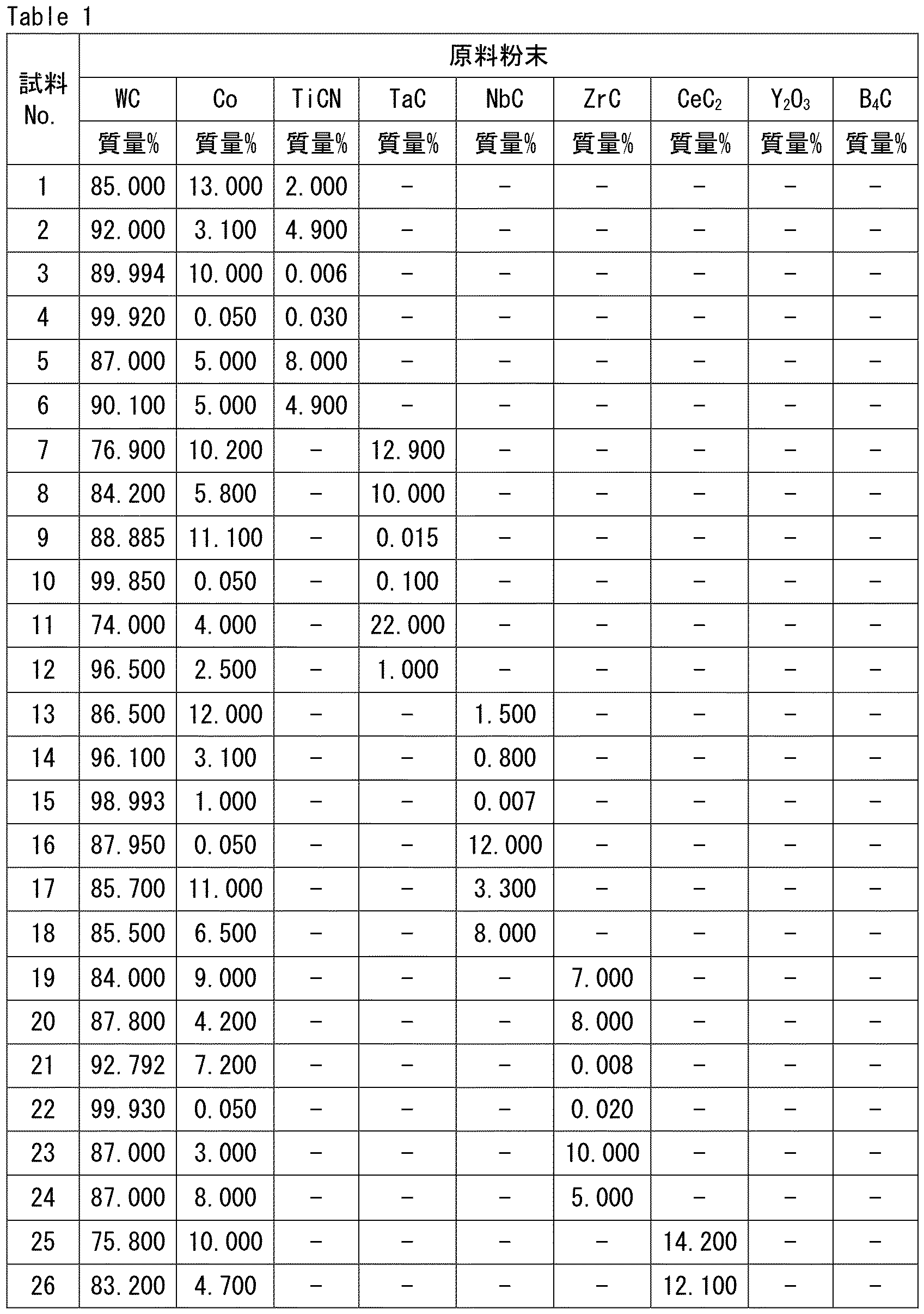


≪試料1~試料48≫
メディア径6mm、回転数100rpm、充填率40%、混合時間20時間。
≪試料49~試料76≫
メディア径6mm、回転数100rpm、充填率40%、混合時間10時間。
≪試料1~試料48≫
第1焼結工程:Arガス中で圧力0.1MPa、温度1400℃で400分保持。
第2焼結工程:Arガス中で圧力5MPa、温度1350℃で300分保持。
≪試料49~試料76≫
第1焼結工程:Arガス中で圧力0.1MPa、温度1400℃で60分保持。
第2焼結工程:なし。
得られた超硬合金を加工し、刃先交換型切削工具(形状:エンドミル)を作製した。
<超硬合金の炭化タングステン粒子の含有率(体積%)および結合相の含有率(体積%)>
各試料の超硬合金の炭化タングステン粒子の含有率(体積%)および結合相の含有率(体積%)を測定した。具体的な測定方法は実施形態1に記載の通りである。結果を表4~表6の「超硬合金」の「WC粒子含有率」および「結合相含有率」欄に示す。更に、超硬合金の炭化タングステン粒子の含有率および結合相の含有率の合計を表4~表6の「超硬合金」の「WC粒子+結合相含有率」欄に示す。表4~表6において、「WC粒子+結合相含有率」欄が100体積%未満の超硬合金は、第1元素を含む化合物の析出物や固溶体(例えば、TiCNやTaC)などを含むことが確認された。
各試料の超硬合金において、結合相中のコバルト含有率を測定した。具体的な測定方法は実施形態1に記載の通りである。結果を表4~表6の「超硬合金」の「結合相中のCo含有率」欄に示す。
各試料の超硬合金において、超硬合金の第1元素の種類および合計含有率を測定した。具体的な測定方法は実施形態1に記載の通りである。結果を表7~表9の「超硬合金」の「第1元素種類」および「第1元素合計含有率」欄に示す。
各試料の超硬合金において、実施形態1に示されるライン分析を行い、第1グラフを得た。各試料の第1グラフにおいて、原点に最も近いタングステンのピークW1と、ピークW1に最も近いタングステンの他のピークW2との間に、第1元素のそれぞれの最大ピークMが存在するか否かを確認した。結果を表7~表9の「超硬合金」の「最大ピークM」欄に示す。「有」とは、最大ピークMが存在することを示し、「無」とは、最大ピークMが存在しないことを示す。最大ピークMが複数存在する場合は、全ての最大ピークがW1とW2との間に存在する場合「有」と示す。

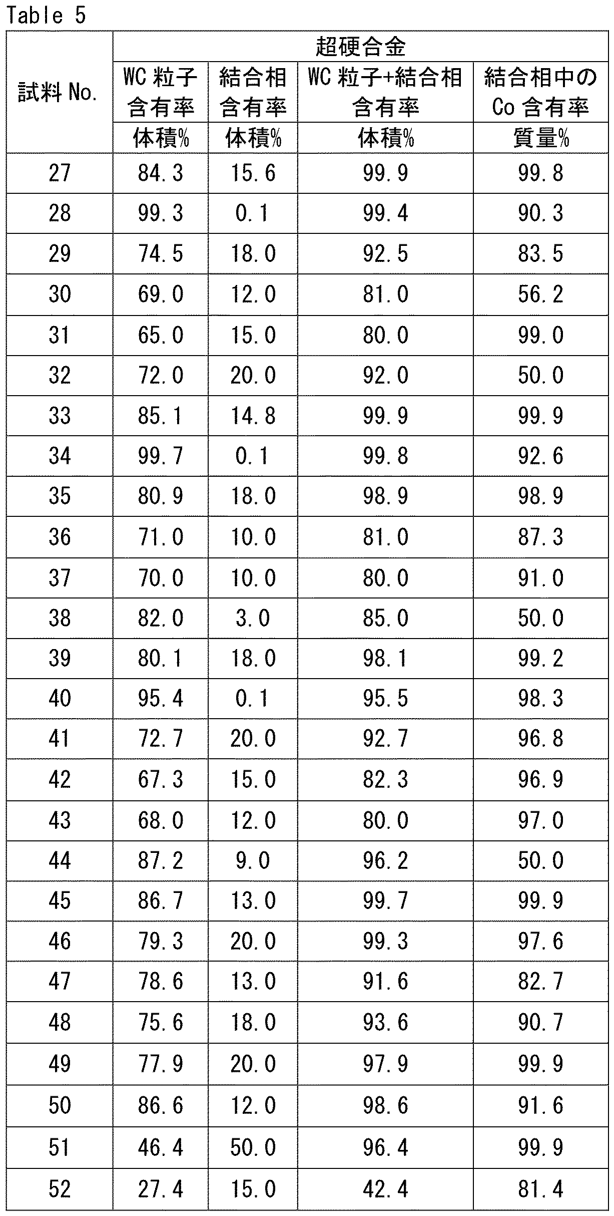


各試料の切削工具を用いて以下の条件でエンドミル加工を行い、切削距離0.01m毎に、逃げ面の損傷幅を測定した。損傷幅とは、摩耗やチッピングにより生じる逃げ面の損傷の最大長さを意味する。最大長さは、摩耗の場合は、最大摩耗量に該当し、チッピングの場合は、最大欠損長さに該当する。損傷幅が0.1mmに到達した時点の切削距離を工具寿命とする。結果を表7~表9の「切削試験」欄に示す。切削距離が長いほど、工具寿命が長いことを示す。
被削材:インコネル
加工:側面加工
切削速度:120m/min
1刃当たりの送り量fz:0.1mm/t
軸方向の切込み深さap:0.2mm
半径方向の切込み深さae:0.2mm
切削液:水溶性切削油
上記の切削条件は、難削材の高速加工に該当する。
試料1~試料48の超硬合金および切削工具は、実施例に該当する。試料49~試料76の超硬合金および切削工具は、比較例に該当する。試料1~試料48(実施例)の切削工具は、試料49~試料76(比較例)の切削工具に比べて、難削材の高速加工において、長い工具寿命を示すことが確認された。これは、試料1~試料48(実施例)の超硬合金は、ピークMを有し、かつ、割合IB/IAは、0.5以下であるため、耐溶着性が向上し、溶着に伴う摩耗や欠損の発生が抑制されたためと推察される。
Claims (3)
- 複数の炭化タングステン粒子と、結合相と、を備える超硬合金であって、
前記超硬合金は、前記炭化タングステン粒子および前記結合相を合計で80体積%以上含み、
前記超硬合金は、前記結合相を0.1体積%以上20体積%以下含み、
前記超硬合金は、チタン、タンタル、ニオブ、ジルコニウム、セリウム、イットリウムおよび硼素からなる群より選ばれる少なくとも1つの第1元素を含み、
前記超硬合金は、前記第1元素を合計で0.01原子%以上20原子%以下含み、
前記結合相は、コバルトを50質量%以上含み、
互いに隣接する前記結合相から前記炭化タングステン粒子に向かう第1方向に沿って、透過型電子顕微鏡に付属のエネルギー分散型X線分光装置を用いてライン分析を行って得られた結果を、X軸がコバルトが最大強度を示す位置からの距離、かつ、Y軸が規格化された強度である座標系に示した第1グラフにおいて、
原点に最も近いタングステンのピークW1と、前記ピークW1に最も近いタングステンの他のピークW2との間に、前記第1元素のそれぞれの最大ピークMが存在し、
前記第1元素のそれぞれにおいて、前記最大ピークMの最大ピーク強度IAに対する、強度IBの割合IB/IAは、0.5以下であり、
前記強度IBは、前記最大ピーク強度IAの距離P1から、前記原点と反対側への距離が0.2nmである距離P2における前記第1元素の強度である、超硬合金。 - 前記超硬合金は、前記結合相を18体積%以下含む、請求項1に記載の超硬合金。
- 請求項1または請求項2に記載の超硬合金からなる刃先を備える、切削工具。
Priority Applications (6)
| Application Number | Priority Date | Filing Date | Title |
|---|---|---|---|
| PCT/JP2023/027732 WO2025027677A1 (ja) | 2023-07-28 | 2023-07-28 | 超硬合金および切削工具 |
| JP2023577962A JP7589839B1 (ja) | 2023-07-28 | 2023-07-28 | 超硬合金および切削工具 |
| US18/686,491 US12109630B1 (en) | 2023-07-28 | 2023-07-28 | Cemented carbide and cutting tool |
| CN202380047054.0A CN119731358A (zh) | 2023-07-28 | 2023-07-28 | 硬质合金以及切削工具 |
| EP23935623.1A EP4527962A4 (en) | 2023-07-28 | 2023-07-28 | CEMENTED CARBIDE AND CUTTING TOOL |
| TW113114910A TW202509245A (zh) | 2023-07-28 | 2024-04-22 | 超硬合金及切削工具 |
Applications Claiming Priority (1)
| Application Number | Priority Date | Filing Date | Title |
|---|---|---|---|
| PCT/JP2023/027732 WO2025027677A1 (ja) | 2023-07-28 | 2023-07-28 | 超硬合金および切削工具 |
Publications (1)
| Publication Number | Publication Date |
|---|---|
| WO2025027677A1 true WO2025027677A1 (ja) | 2025-02-06 |
Family
ID=92936142
Family Applications (1)
| Application Number | Title | Priority Date | Filing Date |
|---|---|---|---|
| PCT/JP2023/027732 Pending WO2025027677A1 (ja) | 2023-07-28 | 2023-07-28 | 超硬合金および切削工具 |
Country Status (6)
| Country | Link |
|---|---|
| US (1) | US12109630B1 (ja) |
| EP (1) | EP4527962A4 (ja) |
| JP (1) | JP7589839B1 (ja) |
| CN (1) | CN119731358A (ja) |
| TW (1) | TW202509245A (ja) |
| WO (1) | WO2025027677A1 (ja) |
Citations (9)
| Publication number | Priority date | Publication date | Assignee | Title |
|---|---|---|---|---|
| JP2000336451A (ja) * | 1999-05-28 | 2000-12-05 | Toshiba Tungaloy Co Ltd | 改質焼結合金、被覆焼結合金及びその製造方法 |
| JP2005068515A (ja) * | 2003-08-26 | 2005-03-17 | Hitachi Tool Engineering Ltd | 微粒超硬合金 |
| JP2016020540A (ja) * | 2014-06-17 | 2016-02-04 | 住友電気工業株式会社 | 超硬合金及び切削工具 |
| JP2016098393A (ja) | 2014-11-20 | 2016-05-30 | 日本特殊合金株式会社 | 超硬合金 |
| WO2019116614A1 (ja) * | 2017-12-11 | 2019-06-20 | 住友電工ハードメタル株式会社 | 超硬合金及び切削工具 |
| JP2021110010A (ja) | 2020-01-14 | 2021-08-02 | 日本特殊合金株式会社 | 超微粒超硬合金,およびこれを用いた切断用もしくは切削用工具または耐摩耗用工具 |
| JP2022109485A (ja) * | 2021-01-15 | 2022-07-28 | 株式会社Moldino | Wc基超硬合金および該合金を用いた切削工具 |
| WO2022172729A1 (ja) * | 2021-02-15 | 2022-08-18 | 住友電気工業株式会社 | 超硬合金及びそれを基材として含む切削工具 |
| JP7311826B1 (ja) * | 2022-03-15 | 2023-07-20 | 住友電気工業株式会社 | 超硬合金 |
Family Cites Families (1)
| Publication number | Priority date | Publication date | Assignee | Title |
|---|---|---|---|---|
| JP7251691B1 (ja) * | 2022-01-20 | 2023-04-04 | 住友電気工業株式会社 | 超硬合金およびそれを含む工具 |
-
2023
- 2023-07-28 EP EP23935623.1A patent/EP4527962A4/en active Pending
- 2023-07-28 US US18/686,491 patent/US12109630B1/en active Active
- 2023-07-28 WO PCT/JP2023/027732 patent/WO2025027677A1/ja active Pending
- 2023-07-28 CN CN202380047054.0A patent/CN119731358A/zh active Pending
- 2023-07-28 JP JP2023577962A patent/JP7589839B1/ja active Active
-
2024
- 2024-04-22 TW TW113114910A patent/TW202509245A/zh unknown
Patent Citations (9)
| Publication number | Priority date | Publication date | Assignee | Title |
|---|---|---|---|---|
| JP2000336451A (ja) * | 1999-05-28 | 2000-12-05 | Toshiba Tungaloy Co Ltd | 改質焼結合金、被覆焼結合金及びその製造方法 |
| JP2005068515A (ja) * | 2003-08-26 | 2005-03-17 | Hitachi Tool Engineering Ltd | 微粒超硬合金 |
| JP2016020540A (ja) * | 2014-06-17 | 2016-02-04 | 住友電気工業株式会社 | 超硬合金及び切削工具 |
| JP2016098393A (ja) | 2014-11-20 | 2016-05-30 | 日本特殊合金株式会社 | 超硬合金 |
| WO2019116614A1 (ja) * | 2017-12-11 | 2019-06-20 | 住友電工ハードメタル株式会社 | 超硬合金及び切削工具 |
| JP2021110010A (ja) | 2020-01-14 | 2021-08-02 | 日本特殊合金株式会社 | 超微粒超硬合金,およびこれを用いた切断用もしくは切削用工具または耐摩耗用工具 |
| JP2022109485A (ja) * | 2021-01-15 | 2022-07-28 | 株式会社Moldino | Wc基超硬合金および該合金を用いた切削工具 |
| WO2022172729A1 (ja) * | 2021-02-15 | 2022-08-18 | 住友電気工業株式会社 | 超硬合金及びそれを基材として含む切削工具 |
| JP7311826B1 (ja) * | 2022-03-15 | 2023-07-20 | 住友電気工業株式会社 | 超硬合金 |
Non-Patent Citations (1)
| Title |
|---|
| See also references of EP4527962A4 |
Also Published As
| Publication number | Publication date |
|---|---|
| EP4527962A1 (en) | 2025-03-26 |
| EP4527962A4 (en) | 2025-11-19 |
| US12109630B1 (en) | 2024-10-08 |
| CN119731358A (zh) | 2025-03-28 |
| JPWO2025027677A1 (ja) | 2025-02-06 |
| JP7589839B1 (ja) | 2024-11-26 |
| TW202509245A (zh) | 2025-03-01 |
Similar Documents
| Publication | Publication Date | Title |
|---|---|---|
| JP6459106B1 (ja) | 超硬合金及び切削工具 | |
| WO2019138599A1 (ja) | 超硬合金及び切削工具 | |
| CN117677724A (zh) | 硬质合金以及包含该硬质合金的工具 | |
| JP7517483B2 (ja) | 超硬合金及びそれを基材として含む切削工具 | |
| JP7501798B1 (ja) | 超硬合金およびそれを用いた切削工具 | |
| JP7589839B1 (ja) | 超硬合金および切削工具 | |
| JP7589840B1 (ja) | 超硬合金および切削工具 | |
| JP7666745B1 (ja) | 超硬合金および切削工具 | |
| JP7251691B1 (ja) | 超硬合金およびそれを含む工具 | |
| JP7616426B1 (ja) | 超硬合金およびそれを用いた切削工具 | |
| JP2025076775A (ja) | 超硬合金および切削工具 | |
| JP7501800B1 (ja) | 超硬合金およびそれを用いた切削工具 | |
| JP7670234B1 (ja) | 超硬合金および切削工具 | |
| JP7782777B1 (ja) | 超硬合金および切削工具 | |
| JP7666744B1 (ja) | 超硬合金および切削工具 | |
| JP7533839B1 (ja) | 超硬合金および切削工具 | |
| JP7593561B1 (ja) | 超硬合金および切削工具 | |
| WO2026088288A1 (ja) | 超硬合金および切削工具 | |
| CN120457227A (zh) | 硬质合金 | |
| CN121605209A (zh) | 硬质合金以及切削工具 |
Legal Events
| Date | Code | Title | Description |
|---|---|---|---|
| WWE | Wipo information: entry into national phase |
Ref document number: 2023577962 Country of ref document: JP |
|
| ENP | Entry into the national phase |
Ref document number: 2023935623 Country of ref document: EP Effective date: 20241106 |
|
| WWE | Wipo information: entry into national phase |
Ref document number: 202380047054.0 Country of ref document: CN |
|
| 121 | Ep: the epo has been informed by wipo that ep was designated in this application |
Ref document number: 23935623 Country of ref document: EP Kind code of ref document: A1 |
|
| WWP | Wipo information: published in national office |
Ref document number: 202380047054.0 Country of ref document: CN |
|
| NENP | Non-entry into the national phase |
Ref country code: DE |