WO2025100245A1 - 電力生成装置 - Google Patents
電力生成装置 Download PDFInfo
- Publication number
- WO2025100245A1 WO2025100245A1 PCT/JP2024/037861 JP2024037861W WO2025100245A1 WO 2025100245 A1 WO2025100245 A1 WO 2025100245A1 JP 2024037861 W JP2024037861 W JP 2024037861W WO 2025100245 A1 WO2025100245 A1 WO 2025100245A1
- Authority
- WO
- WIPO (PCT)
- Prior art keywords
- wiring
- phase
- power
- diode bridge
- converter
- Prior art date
- Legal status (The legal status is an assumption and is not a legal conclusion. Google has not performed a legal analysis and makes no representation as to the accuracy of the status listed.)
- Pending
Links
Images



Classifications
-
- H—ELECTRICITY
- H02—GENERATION; CONVERSION OR DISTRIBUTION OF ELECTRIC POWER
- H02M—APPARATUS FOR CONVERSION BETWEEN AC AND AC, BETWEEN AC AND DC, OR BETWEEN DC AND DC, AND FOR USE WITH MAINS OR SIMILAR POWER SUPPLY SYSTEMS; CONVERSION OF DC OR AC INPUT POWER INTO SURGE OUTPUT POWER; CONTROL OR REGULATION THEREOF
- H02M7/00—Conversion of AC power input into DC power output; Conversion of DC power input into AC power output
- H02M7/003—Constructional details, e.g. physical layout, assembly, wiring or busbar connections
-
- H—ELECTRICITY
- H02—GENERATION; CONVERSION OR DISTRIBUTION OF ELECTRIC POWER
- H02M—APPARATUS FOR CONVERSION BETWEEN AC AND AC, BETWEEN AC AND DC, OR BETWEEN DC AND DC, AND FOR USE WITH MAINS OR SIMILAR POWER SUPPLY SYSTEMS; CONVERSION OF DC OR AC INPUT POWER INTO SURGE OUTPUT POWER; CONTROL OR REGULATION THEREOF
- H02M1/00—Details of apparatus for conversion
- H02M1/0067—Converter structures employing plural converter units, other than for parallel operation of the units on a single load
- H02M1/008—Plural converter units for generating at two or more independent and non-parallel outputs, e.g. systems with plural point of load switching regulators
-
- H—ELECTRICITY
- H02—GENERATION; CONVERSION OR DISTRIBUTION OF ELECTRIC POWER
- H02M—APPARATUS FOR CONVERSION BETWEEN AC AND AC, BETWEEN AC AND DC, OR BETWEEN DC AND DC, AND FOR USE WITH MAINS OR SIMILAR POWER SUPPLY SYSTEMS; CONVERSION OF DC OR AC INPUT POWER INTO SURGE OUTPUT POWER; CONTROL OR REGULATION THEREOF
- H02M5/00—Conversion of AC power input into AC power output, e.g. for change of voltage, for change of frequency, for change of number of phases
- H02M5/40—Conversion of AC power input into AC power output, e.g. for change of voltage, for change of frequency, for change of number of phases with intermediate conversion into DC
- H02M5/42—Conversion of AC power input into AC power output, e.g. for change of voltage, for change of frequency, for change of number of phases with intermediate conversion into DC by static converters
- H02M5/44—Conversion of AC power input into AC power output, e.g. for change of voltage, for change of frequency, for change of number of phases with intermediate conversion into DC by static converters using discharge tubes or semiconductor devices to convert the intermediate DC into AC
- H02M5/453—Conversion of AC power input into AC power output, e.g. for change of voltage, for change of frequency, for change of number of phases with intermediate conversion into DC by static converters using discharge tubes or semiconductor devices to convert the intermediate DC into AC using devices of a triode or transistor type requiring continuous application of a control signal
- H02M5/458—Conversion of AC power input into AC power output, e.g. for change of voltage, for change of frequency, for change of number of phases with intermediate conversion into DC by static converters using discharge tubes or semiconductor devices to convert the intermediate DC into AC using devices of a triode or transistor type requiring continuous application of a control signal using semiconductor devices only
-
- H—ELECTRICITY
- H02—GENERATION; CONVERSION OR DISTRIBUTION OF ELECTRIC POWER
- H02M—APPARATUS FOR CONVERSION BETWEEN AC AND AC, BETWEEN AC AND DC, OR BETWEEN DC AND DC, AND FOR USE WITH MAINS OR SIMILAR POWER SUPPLY SYSTEMS; CONVERSION OF DC OR AC INPUT POWER INTO SURGE OUTPUT POWER; CONTROL OR REGULATION THEREOF
- H02M7/00—Conversion of AC power input into DC power output; Conversion of DC power input into AC power output
- H02M7/02—Conversion of AC power input into DC power output without possibility of reversal
- H02M7/04—Conversion of AC power input into DC power output without possibility of reversal by static converters
- H02M7/06—Conversion of AC power input into DC power output without possibility of reversal by static converters using discharge tubes without control electrode or semiconductor devices without control electrode
-
- H—ELECTRICITY
- H02—GENERATION; CONVERSION OR DISTRIBUTION OF ELECTRIC POWER
- H02M—APPARATUS FOR CONVERSION BETWEEN AC AND AC, BETWEEN AC AND DC, OR BETWEEN DC AND DC, AND FOR USE WITH MAINS OR SIMILAR POWER SUPPLY SYSTEMS; CONVERSION OF DC OR AC INPUT POWER INTO SURGE OUTPUT POWER; CONTROL OR REGULATION THEREOF
- H02M7/00—Conversion of AC power input into DC power output; Conversion of DC power input into AC power output
- H02M7/02—Conversion of AC power input into DC power output without possibility of reversal
- H02M7/04—Conversion of AC power input into DC power output without possibility of reversal by static converters
- H02M7/12—Conversion of AC power input into DC power output without possibility of reversal by static converters using discharge tubes with control electrode or semiconductor devices with control electrode
- H02M7/145—Conversion of AC power input into DC power output without possibility of reversal by static converters using discharge tubes with control electrode or semiconductor devices with control electrode using devices of a thyratron or thyristor type requiring extinguishing means
- H02M7/155—Conversion of AC power input into DC power output without possibility of reversal by static converters using discharge tubes with control electrode or semiconductor devices with control electrode using devices of a thyratron or thyristor type requiring extinguishing means using semiconductor devices only
- H02M7/162—Conversion of AC power input into DC power output without possibility of reversal by static converters using discharge tubes with control electrode or semiconductor devices with control electrode using devices of a thyratron or thyristor type requiring extinguishing means using semiconductor devices only in a bridge configuration
-
- H—ELECTRICITY
- H02—GENERATION; CONVERSION OR DISTRIBUTION OF ELECTRIC POWER
- H02M—APPARATUS FOR CONVERSION BETWEEN AC AND AC, BETWEEN AC AND DC, OR BETWEEN DC AND DC, AND FOR USE WITH MAINS OR SIMILAR POWER SUPPLY SYSTEMS; CONVERSION OF DC OR AC INPUT POWER INTO SURGE OUTPUT POWER; CONTROL OR REGULATION THEREOF
- H02M7/00—Conversion of AC power input into DC power output; Conversion of DC power input into AC power output
- H02M7/02—Conversion of AC power input into DC power output without possibility of reversal
- H02M7/04—Conversion of AC power input into DC power output without possibility of reversal by static converters
- H02M7/12—Conversion of AC power input into DC power output without possibility of reversal by static converters using discharge tubes with control electrode or semiconductor devices with control electrode
- H02M7/21—Conversion of AC power input into DC power output without possibility of reversal by static converters using discharge tubes with control electrode or semiconductor devices with control electrode using devices of a triode or transistor type requiring continuous application of a control signal
- H02M7/217—Conversion of AC power input into DC power output without possibility of reversal by static converters using discharge tubes with control electrode or semiconductor devices with control electrode using devices of a triode or transistor type requiring continuous application of a control signal using semiconductor devices only
- H02M7/219—Conversion of AC power input into DC power output without possibility of reversal by static converters using discharge tubes with control electrode or semiconductor devices with control electrode using devices of a triode or transistor type requiring continuous application of a control signal using semiconductor devices only in a bridge configuration
-
- H—ELECTRICITY
- H02—GENERATION; CONVERSION OR DISTRIBUTION OF ELECTRIC POWER
- H02M—APPARATUS FOR CONVERSION BETWEEN AC AND AC, BETWEEN AC AND DC, OR BETWEEN DC AND DC, AND FOR USE WITH MAINS OR SIMILAR POWER SUPPLY SYSTEMS; CONVERSION OF DC OR AC INPUT POWER INTO SURGE OUTPUT POWER; CONTROL OR REGULATION THEREOF
- H02M7/00—Conversion of AC power input into DC power output; Conversion of DC power input into AC power output
- H02M7/42—Conversion of DC power input into AC power output without possibility of reversal
- H02M7/44—Conversion of DC power input into AC power output without possibility of reversal by static converters
- H02M7/48—Conversion of DC power input into AC power output without possibility of reversal by static converters using discharge tubes with control electrode or semiconductor devices with control electrode
- H02M7/493—Conversion of DC power input into AC power output without possibility of reversal by static converters using discharge tubes with control electrode or semiconductor devices with control electrode the static converters being arranged for operation in parallel
-
- H—ELECTRICITY
- H02—GENERATION; CONVERSION OR DISTRIBUTION OF ELECTRIC POWER
- H02M—APPARATUS FOR CONVERSION BETWEEN AC AND AC, BETWEEN AC AND DC, OR BETWEEN DC AND DC, AND FOR USE WITH MAINS OR SIMILAR POWER SUPPLY SYSTEMS; CONVERSION OF DC OR AC INPUT POWER INTO SURGE OUTPUT POWER; CONTROL OR REGULATION THEREOF
- H02M7/00—Conversion of AC power input into DC power output; Conversion of DC power input into AC power output
- H02M7/42—Conversion of DC power input into AC power output without possibility of reversal
- H02M7/44—Conversion of DC power input into AC power output without possibility of reversal by static converters
- H02M7/48—Conversion of DC power input into AC power output without possibility of reversal by static converters using discharge tubes with control electrode or semiconductor devices with control electrode
- H02M7/53—Conversion of DC power input into AC power output without possibility of reversal by static converters using discharge tubes with control electrode or semiconductor devices with control electrode using devices of a triode or transistor type requiring continuous application of a control signal
- H02M7/537—Conversion of DC power input into AC power output without possibility of reversal by static converters using discharge tubes with control electrode or semiconductor devices with control electrode using devices of a triode or transistor type requiring continuous application of a control signal using semiconductor devices only, e.g. single switched pulse inverters
- H02M7/5387—Conversion of DC power input into AC power output without possibility of reversal by static converters using discharge tubes with control electrode or semiconductor devices with control electrode using devices of a triode or transistor type requiring continuous application of a control signal using semiconductor devices only, e.g. single switched pulse inverters in a bridge configuration
-
- H—ELECTRICITY
- H02—GENERATION; CONVERSION OR DISTRIBUTION OF ELECTRIC POWER
- H02M—APPARATUS FOR CONVERSION BETWEEN AC AND AC, BETWEEN AC AND DC, OR BETWEEN DC AND DC, AND FOR USE WITH MAINS OR SIMILAR POWER SUPPLY SYSTEMS; CONVERSION OF DC OR AC INPUT POWER INTO SURGE OUTPUT POWER; CONTROL OR REGULATION THEREOF
- H02M7/00—Conversion of AC power input into DC power output; Conversion of DC power input into AC power output
- H02M7/42—Conversion of DC power input into AC power output without possibility of reversal
- H02M7/44—Conversion of DC power input into AC power output without possibility of reversal by static converters
- H02M7/48—Conversion of DC power input into AC power output without possibility of reversal by static converters using discharge tubes with control electrode or semiconductor devices with control electrode
- H02M7/53—Conversion of DC power input into AC power output without possibility of reversal by static converters using discharge tubes with control electrode or semiconductor devices with control electrode using devices of a triode or transistor type requiring continuous application of a control signal
- H02M7/537—Conversion of DC power input into AC power output without possibility of reversal by static converters using discharge tubes with control electrode or semiconductor devices with control electrode using devices of a triode or transistor type requiring continuous application of a control signal using semiconductor devices only, e.g. single switched pulse inverters
- H02M7/539—Conversion of DC power input into AC power output without possibility of reversal by static converters using discharge tubes with control electrode or semiconductor devices with control electrode using devices of a triode or transistor type requiring continuous application of a control signal using semiconductor devices only, e.g. single switched pulse inverters with automatic control of output wave form or frequency
- H02M7/5395—Conversion of DC power input into AC power output without possibility of reversal by static converters using discharge tubes with control electrode or semiconductor devices with control electrode using devices of a triode or transistor type requiring continuous application of a control signal using semiconductor devices only, e.g. single switched pulse inverters with automatic control of output wave form or frequency by pulse-width modulation
-
- H—ELECTRICITY
- H02—GENERATION; CONVERSION OR DISTRIBUTION OF ELECTRIC POWER
- H02P—CONTROL OR REGULATION OF ELECTRIC MOTORS, ELECTRIC GENERATORS OR DYNAMO-ELECTRIC CONVERTERS; CONTROLLING TRANSFORMERS, REACTORS OR CHOKE COILS
- H02P27/00—Arrangements or methods for the control of AC motors characterised by the kind of supply voltage
- H02P27/04—Arrangements or methods for the control of AC motors characterised by the kind of supply voltage using variable-frequency supply voltage, e.g. inverter or converter supply voltage
- H02P27/06—Arrangements or methods for the control of AC motors characterised by the kind of supply voltage using variable-frequency supply voltage, e.g. inverter or converter supply voltage using DC to AC converters or inverters
- H02P27/08—Arrangements or methods for the control of AC motors characterised by the kind of supply voltage using variable-frequency supply voltage, e.g. inverter or converter supply voltage using DC to AC converters or inverters with pulse width modulation
-
- H—ELECTRICITY
- H02—GENERATION; CONVERSION OR DISTRIBUTION OF ELECTRIC POWER
- H02P—CONTROL OR REGULATION OF ELECTRIC MOTORS, ELECTRIC GENERATORS OR DYNAMO-ELECTRIC CONVERTERS; CONTROLLING TRANSFORMERS, REACTORS OR CHOKE COILS
- H02P5/00—Arrangements specially adapted for regulating or controlling the speed or torque of two or more electric motors
- H02P5/74—Arrangements specially adapted for regulating or controlling the speed or torque of two or more electric motors controlling two or more AC dynamo-electric motors
Definitions
- This relates to a power generation device installed in a three-phase, four-wire, 400V air conditioner.
- the 400V converter circuit mounted in the outdoor unit is generally composed of one three-phase diode bridge, as disclosed in Patent Document 1 (JP Patent Publication No. 2012-165509), for example.
- the power generating device of the first aspect is a power generating device mounted on a printed wiring board, and includes an input terminal, a first wiring, a second wiring, a third wiring, and a fourth wiring, a first converter, a fifth wiring, and a second converter.
- the input terminal is configured to receive the R phase, the S phase, the T phase, and the N phase from a power source that supplies three-phase AC in a three-phase four-wire system.
- the first wiring, the second wiring, the third wiring, and the fourth wiring are connected to the R phase, the S phase, the T phase, and the N phase, respectively, via the input terminal.
- the first converter includes a first diode bridge connected between two power supply lines selected as a first combination from the three power supply lines of the first wiring, the second wiring, and the third wiring, and a second diode bridge connected between two power supply lines selected as a second combination different from the first combination from the three power supply lines, and converts AC power into DC power.
- the fifth wiring branches off from any one of the first wiring, the second wiring, and the third wiring.
- the second converter includes a third diode bridge connected between the fourth wiring and the fifth wiring, and converts AC power into DC power.
- one input of the second converter is connected to one of the first, second, and third wiring between the input terminal and the first converter, and the other input of the second converter is connected to the fourth wire (N phase), so that an increase in the value of the current flowing through the first diode bridge and second diode bridge of the first converter can be suppressed.
- the power generating device of the second aspect is a power generating device mounted on a printed wiring board, and includes an input terminal, a first wiring, a second wiring, a third wiring, and a fourth wiring, a first converter, a fifth wiring, and a second converter.
- the input terminal is configured to receive the R phase, the S phase, the T phase, and the N phase from a power source that supplies three-phase AC in a three-phase four-wire system.
- the first wiring, the second wiring, the third wiring, and the fourth wiring are connected to the R phase, the S phase, the T phase, and the N phase, respectively, via the input terminal.
- the first converter includes a first diode bridge connected to one power supply line selected from the three power supply lines of the first wiring, the second wiring, and the third wiring, and a second diode bridge connected between the remaining two power supply lines, and converts AC power into DC power.
- the fifth wiring branches off from one of the first wiring, the second wiring, and the third wiring.
- the second converter includes a third diode bridge connected between the fourth wiring and the fifth wiring, and converts AC power into DC power.
- one input of the second converter is connected to one of the first, second, and third wiring between the input terminal and the first converter, and the other input of the second converter is connected to the fourth wire (N phase), so that an increase in the value of the current flowing through the first diode bridge and second diode bridge of the first converter can be suppressed.
- the power generating device of the third aspect is the power generating device of the first or second aspect, in which the branching point of the fifth wiring is located between the center position of the length of the wiring from which the fifth wiring branches and the input terminal.
- the branch point of the fifth wiring is separated from the first converter by a distance that is at least half of the section from the input terminal to the first converter. In this way, by separating the branch point of the fifth wiring from the first converter, heat generated at the branch point of the fifth wiring is less likely to be conducted to the first converter, and heat concentration around the terminals of the first converter is suppressed.
- the power generating device of the fourth aspect is any one of the power generating devices of the first aspect to the third aspect, and further includes a sixth wiring, a seventh wiring, and a third converter.
- the sixth wiring and the seventh wiring branch off from any two wirings of the first wiring, the second wiring, and the third wiring.
- the third converter includes a fourth diode bridge connected between the sixth wiring and the seventh wiring, and converts AC power into DC power.
- each of the two inputs of the third converter is connected to two of the first wiring, the second wiring, and the third wiring between the input terminal and the first converter, so that an increase in the value of the current flowing through the first diode bridge and the second diode bridge of the first converter can be suppressed.
- the power generating device of the fifth aspect is any one of the power generating devices of the first aspect to the fourth aspect, in which the first diode bridge and the second diode bridge are each a diode module in which four bridge-connected diode chips are built into one package.
- the two diode modules are mounted on the first surface of a printed wiring board.
- the power generating device of the sixth aspect is the power generating device of the fifth aspect, in which the diode module has a terminal group and a terminal arrangement surface on which the terminal group is arranged.
- the diode module has a terminal group and a terminal arrangement surface on which the terminal group is arranged.
- the terminal group two AC input terminals and two DC output terminals are arranged in a row in the first direction.
- the two diode modules are spaced apart such that the respective terminal groups have a creepage distance of 3.2 mm or more, and are arranged such that the respective terminal arrangement surfaces do not face each other.
- the terminal groups of the two diode modules do not face each other, which reduces heat concentration on the terminals and conductive patterns.
- the seventh aspect of the power generating device is the fifth aspect of the power generating device, in which the diode module has a heat sink.
- the eighth aspect of the power generating device is the fifth aspect of the power generating device, in which the diode module has two AC input terminals and two DC output terminals. At least one of a varistor and a surge absorber is connected between the two AC input terminals.
- This power generation device can limit the voltage between the AC input terminals to a specified value even if a voltage exceeding a specified value is applied between the AC input terminals.
- the power generating device of the ninth aspect is the power generating device of the fifth aspect, in which the diode module has two AC input terminals and two DC output terminals. At least one of a varistor and a film capacitor is connected between the two DC output terminals.
- This power generating device absorbs external pulses or power supply noise, and also prevents noise from being transmitted to the AC power supply.
- the power generating device of the tenth aspect is any one of the power generating devices of the first aspect to the ninth aspect, further comprising a first inverter circuit connected between the output terminals of the first converter.
- the first inverter circuit is a power module in which an upper arm switching element and a lower arm switching element are built into a single package, and is mounted on a first surface of a printed wiring board.
- modularization makes it easier to design the peripheral circuits on the first surface of the printed wiring board, which is the mounting surface.
- the power generating device of an eleventh aspect is any one of the power generating devices of the first aspect to the tenth aspect, further comprising a second inverter circuit connected between the output terminals of the second converter.
- the second inverter circuit is a power module in which an upper arm switching element and a lower arm switching element are built into a single package, and is mounted on a first surface of a printed wiring board.
- modularization makes it easier to design the peripheral circuits on the first surface of the printed wiring board, which is the mounting surface.
- the power generating device of the twelfth aspect is any one of the power generating devices of the first aspect to the eleventh aspect, in which the printed wiring board is a multilayer printed wiring board having multiple conductive pattern layers stacked with insulating layers sandwiched therebetween.
- conductive patterns can be wired not only on the surface of the printed wiring board but also on the inner layers, allowing components to be mounted at high density.
- the power generating device of a thirteenth aspect is the power generating device of the fifth aspect, further comprising a first inverter circuit, a second inverter circuit, and one heat sink.
- the first inverter circuit is connected between output terminals of the first converter.
- the second inverter circuit is connected between output terminals of the second converter.
- Each of the first inverter circuit and the second inverter circuit is a power module in which an upper arm switching element and a lower arm switching element are built into a single package, and is mounted on a first surface of a printed wiring board.
- the heat sink cools the two diode modules and the two power modules.
- one heat sink cools two diode modules and two power modules, reducing the number of parts and the installation space.
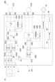
- FIG. 1 is a circuit diagram showing a configuration of a power generating device according to a first embodiment of the present disclosure.
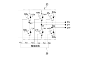
- FIG. 2 is a configuration diagram of an inverter circuit and a drive circuit that drives the inverter circuit.
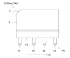
- FIG. 2 is a plan view of a diode module used as a first diode bridge and a second diode bridge.
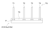
- FIG. 2 is a side view of a diode module used as a first diode bridge and a second diode bridge.
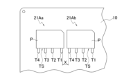
- 4 is a plan view showing mounting positions of a first diode bridge and a second diode bridge on a printed wiring board.
- FIG. 11 is a plan view showing mounting positions of a first diode bridge and a second diode bridge on a printed wiring board in a first modified example.
- FIG. 11 is a plan view showing mounting positions of a first diode bridge and a second diode bridge on a printed wiring board in a second modified example.
- FIG. 13 is a plan view showing mounting positions of a first diode bridge and a second diode bridge on a printed wiring board in a third modified example.
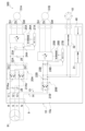
- FIG. 11 is a circuit diagram showing a configuration of a power generating device according to a second embodiment of the present disclosure. 2 is a plan view of a heat sink that cools the first diode bridge, the second diode bridge, the first inverter circuit, and the second inverter circuit.
- FIG. FIG. 1 is a circuit diagram showing a configuration of a power generating device including a first diode bridge connected to one power supply line selected from three power supply lines including a first wiring, a second wiring, and a third wiring, and a second diode bridge connected between the remaining two power supply lines.
- FIG. 2 is another circuit diagram showing the configuration of a power generating device including a first diode bridge connected to one power supply line selected from three power supply lines including a first wiring, a second wiring, and a third wiring, and a second diode bridge connected between the remaining two power supply lines.
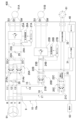
- 11 is a circuit diagram in the case where the wiring method of the first diode bridge in FIG. 10 is applied to FIG. 8 .
- 12 is a circuit diagram in the case where the wiring method of the first diode bridge in FIG. 11 is applied to FIG. 8 .
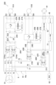
- FIG. 1 is a circuit diagram showing a configuration of a power generating device 100 according to a first embodiment of the present disclosure.
- the power generating device 100 includes a first converter 20A and a second converter 20B, which are mounted on a first surface 10a of a printed wiring board 10.
- the first converter 20A includes a first diode bridge 21Aa connected between two power lines selected as a first combination from the three power lines, the first wiring 11, the second wiring 12, and the third wiring 13, and a second diode bridge 21Ab connected between two power lines selected as a second combination from the three power lines that is different from the first combination.
- the first converter 20A includes a first diode bridge 21Aa connected between a first wiring 11 connected to the R phase and a second wiring 12 connected to the S phase, and a second diode bridge 21Ab connected between the second wiring 12 and a third wiring 13 connected to the T phase, and converts AC power into DC power.
- the second converter 20B includes a third diode bridge 21B connected between a fourth wiring 14 connected to the N phase and a fifth wiring 15 branching off from the first wiring 11, and converts AC power into DC power.
- the power generating device 100 disclosed herein is mounted, for example, in the outdoor unit of a three-phase, four-wire, 400V air conditioner.
- the printed wiring board 10 is a multilayer printed wiring board having a plurality of conductive pattern layers stacked with insulating layers sandwiched therebetween.
- the components of the power generating device 100 namely, the input terminal 9, the first converter 20A, the second converter 20B, the first inverter circuit 25A, the second inverter circuit 25B, the switching power supply 31, the four-way switching valve circuit 32, and multiple microcomputers that control these components, are mounted on the printed wiring board 10.
- the input terminal 9 is configured to receive the R, S, T, and N phases from an AC power source 91 that supplies three-phase AC in a three-phase, four-wire system.
- the first wiring 11, second wiring 12, third wiring 13, and fourth wiring 14, which are conductive patterns, are connected to the R, S, T, and N phases of the AC power source 91, respectively, via the input terminal 9.
- the first converter 20A includes a first diode bridge 21Aa, a second diode bridge 21Ab, and a first smoothing capacitor 22A.
- the first diode bridge 21Aa is a single-phase diode bridge.
- the first diode bridge 21Aa full-wave rectifies the AC power input from the first wiring 11 connected to the R phase and the second wiring 12 connected to the S phase.
- the second diode bridge 21Ab is a single-phase diode bridge.
- the second diode bridge 21Ab full-wave rectifies the AC power input from the second wiring 12 and the third wiring 13 connected to the T phase.
- the first diode bridge 21Aa and the second diode bridge 21Ab are diode modules in which four bridge-connected diode chips are built into one package.
- the first diode bridge 21Aa and the second diode bridge 21Ab are mounted on the first surface 10a of the printed wiring board 10.
- the first smoothing capacitor 22A smoothes the output voltage from the first diode bridge 21Aa and the second diode bridge 21Ab.
- the second converter 20B includes a third diode bridge 21B and a second smoothing capacitor 22B.
- the third diode bridge 21B is a single-phase diode bridge.
- the third diode bridge 21B full-wave rectifies the AC power input from the fourth wiring 14 connected to the N phase and the fifth wiring 15 branching off from the first wiring 11.
- the wiring that branches off the fifth wiring 15 may be any of the first wiring 11, the second wiring 12, and the third wiring 13.
- the third diode bridge 21B is a diode module in which four bridge-connected diode chips are built into one package.
- the second smoothing capacitor 22B smoothes the output voltage from the third diode bridge 21B.
- the voltage detection unit 23A is connected to the output side of the first smoothing capacitor 22A and detects the voltage across the first smoothing capacitor 22A.
- the voltage detection unit 23A is configured such that two resistors connected in series to each other are connected in parallel to the smoothing capacitor 22A, and the voltage across the first smoothing capacitor 22A is divided. The voltage value at the connection point between these two resistors is input to the first microcomputer 27A.
- the voltage detection unit 23B is connected to the output side of the second smoothing capacitor 22B and detects the voltage across the second smoothing capacitor 22B.
- the voltage detection unit 23B is configured such that two resistors connected in series to each other are connected in parallel to the second smoothing capacitor 22B, and the voltage across the second smoothing capacitor 22B is divided. The voltage value at the connection point between these two resistors is input to the second microcomputer 27B.
- the current detection unit 24A is located between the first smoothing capacitor 22A and the first inverter circuit 25A and is connected to the negative output terminal side of the first smoothing capacitor 22A.
- the current detection unit 24A detects the motor current flowing through the first motor 51A after the first motor 51A is started.
- the current detection unit 24A may be configured with an amplifier circuit using a shunt resistor and an operational amplifier that amplifies the voltage across the resistor.
- the motor current detected by the current detection unit 24A is input to the first microcomputer 27A.
- the current detection unit 24B is located between the second smoothing capacitor 22B and the second inverter circuit 25B and is connected to the negative output terminal side of the second smoothing capacitor 22B.
- the current detection unit 24B detects the motor current flowing through the second motor 51B after the second motor 51B is started.
- the current detection unit 24B may be configured with an amplifier circuit using a shunt resistor and an operational amplifier that amplifies the voltage across the resistor.
- the motor current detected by the current detection unit 24B is input to the second microcomputer 27B.
- Second inverter circuit 25B First inverter circuit 25A, second inverter circuit 25B
- the first inverter circuit 25A is connected to the output side of the first smoothing capacitor 22A.
- the second inverter circuit 25B is connected to the output side of the second smoothing capacitor 22B.
- the first inverter circuit 25A and the second inverter circuit 25B have the same configuration, so they will be described as the inverter circuit 25.
- FIG. 2 is a configuration diagram of inverter circuit 25 and drive circuit 26 that drives it.
- inverter circuit 25 includes a number of insulated gate bipolar transistors (hereinafter simply referred to as transistors) Q3a, Q3b, Q4a, Q4b, Q5a, and Q5b as switching elements, and a number of freewheeling diodes D3a, D3b, D4a, D4b, D5a, and D5b.
- transistors insulated gate bipolar transistors
- Transistors Q3a and Q3b, Q4a and Q4b, and Q5a and Q5b are connected in series with each other, and diodes D3a to D5b are connected in parallel with each other so that the collector terminal of the transistor is connected to the cathode terminal of the diode, and the emitter terminal of the transistor is connected to the anode terminal of the diode.
- the inverter circuit 25 generates drive voltages SU, SV, and SW for driving the motor by applying a DC voltage from the converter and turning on and off each of the transistors Q3a to Q5b at the timing instructed by the drive circuit 26.
- These drive voltages SU, SV, and SW are output to the motor from the connection points NU, NV, and NW of the transistors Q3a and Q3b, Q4a and Q4b, and Q5a and Q5b.
- the first inverter circuit 25A and the second inverter circuit 25B are power modules in which upper arm switching elements (Q3a, Q4a, Q5a, D3a, D4a, D5a) and lower arm switching elements (Q3b, Q4b, Q5b, D3b, D4b, D5b) are built into a single package.
- the first inverter circuit 25A and the second inverter circuit 25B are mounted on the first surface 10a of the printed wiring board 10.
- First drive circuit 26A, second drive circuit 26B The first drive circuit 26A changes the on/off state of each of the transistors Q3a to Q5b of the first inverter circuit 25A based on a drive command from the first microcomputer 27A.
- the second drive circuit 26B changes the on/off state of each of the transistors Q3a to Q5b of the second inverter circuit 25B based on a drive command from the second microcomputer 27B.
- the first drive circuit 26A and the second drive circuit 26B have the same configuration, so they will be described as drive circuit 26.
- the drive circuit 26 generates gate control voltages Gu, Gx, Gv, Gy, Gw, and Gz to be applied to the gates of each of the transistors Q3a to Q5b so that drive voltages SU, SV, and SW having duties determined by the microcomputer are output from the inverter circuit 25 to the motor.
- the generated gate control voltages Gu, Gx, Gv, Gy, Gw, and Gz are applied to the gate terminals of the respective transistors Q3a to Q5b.
- First microcomputer 27A, second microcomputer 27B, third microcomputer 40 The first microcomputer 27A is connected to the voltage detection unit 23A, the current detection unit 24A, and the first drive circuit 26A.
- the first microcomputer 27A controls the first drive circuit 26A to drive the first motor 51A.
- the first motor 51A is used as a drive motor for a compressor.
- the second microcomputer 27B is connected to the voltage detection unit 23B, the current detection unit 24B, and the second drive circuit 26B.
- the second microcomputer 27B controls the second drive circuit 26B to drive the second motor 51B.
- the second motor 51B is used as a drive motor for a blower.
- the third microcomputer 40 is a refrigerant control microcomputer.
- the third microcomputer 40 controls the opening degree of the electric expansion valve of the air conditioner, and adjusts the evaporation temperature, degree of superheat, and degree of subcooling of the refrigerant.
- First varistor 28, second varistor 29 A surge absorber or a varistor is connected between the AC input terminals of the first diode bridge 21Aa and the second diode bridge 21Ab as an overvoltage suppression element.
- a first varistor 28 is connected.
- the first varistor 28 limits the voltage between the AC input terminals to a predetermined value when a voltage exceeding a predetermined value is applied between the AC input terminals.
- At least one of an overvoltage suppression element and a noise elimination element is connected between the DC output terminals of the first diode bridge 21Aa and the second diode bridge 21Ab.
- a surge absorber or a varistor is used as the overvoltage suppression element.
- a film capacitor is used as the noise elimination element.
- a second varistor 29 of the overvoltage suppression element is connected. The second varistor 29 is connected between the first smoothing capacitor 22A and the first inverter circuit 25A, and absorbs surges that occur when the switching elements are operating.
- Switching power supply 31 The switching power supply 31 is connected to the output side of the second converter 20B, and supplies power to the first microcomputer 27A, the second microcomputer 27B, and the third microcomputer 40.
- the four-way switching valve circuit 32 is connected to the output side of the second converter 20B.
- the four-way switching valve circuit 32 uses the electric power output from the second converter 20B to switch the flow path of the four-way switching valve 61.
- the four-way switching valve 61 is a valve that switches the circulation direction of the refrigerant in the refrigerant circuit.
- the first converter 20A of the present embodiment has a circuit configuration in which the AC power of a three-phase four-wire AC power supply is full-wave rectified by two diode bridges, a first diode bridge 21Aa and a second diode bridge 21Ab, and has a cost advantage over a circuit configuration in which full-wave rectification is performed by a single three-phase diode bridge.
- the heat resistance of the first diode bridge 21Aa and the second diode bridge 21Ab individually is lower than that of a diode module of a single three-phase diode bridge, so measures to reduce heat generation during operation are necessary.
- the power supply for the switching power supply 31 and the four-way switching valve circuit 32 is not taken from downstream of the first converter 20A.
- the AC power input to the second converter 20B is AC power input from the fourth wiring 14 connected to the N phase and the fifth wiring 15 branched off from the first wiring 11 connected to the R phase.
- the power supply for the switching power supply 31 and the four-way switching valve circuit 32 is taken from downstream of the second converter 20B. This makes it possible to suppress an increase in the current flowing through each of the first diode bridge 21Aa and the second diode bridge 21Ab.
- the branch point of the fifth wiring 15 is located between the center position of the length of the first wiring 11 where the fifth wiring 15 branches off and the input terminal 9. Specifically, the branch point of the fifth wiring 15 is separated from the first converter 20A by a distance of at least half of the section from the input terminal 9 to the first converter 20A. In this way, by separating the branch point of the fifth wiring 15 from the first converter 20A, heat generated at the branch point of the fifth wiring 15 is less likely to be conducted to the first converter 20A, and heat concentration around the terminals of the first diode bridge 21Aa and the second diode bridge 21Ab is suppressed.
- the diode module 21 includes a rectangular parallelepiped package P incorporating four bridge-connected diode chips, and a terminal group TG protruding from one side surface of the package P.
- the terminal group TG includes a first terminal T1, a second terminal T2, a third terminal T3, and a fourth terminal T4.
- the terminal group TG is parallel to the thickness direction of the package P, protrudes from one of the two faces including the two long sides, and is then bent at a right angle.
- the face from which the terminal group TG protrudes is the terminal arrangement face TS.
- An inclined surface C is formed at one corner of the surface that faces parallel to the terminal arrangement surface TS.
- the terminal group TG is arranged in order from the first terminal T1, which is closest to the inclined surface C, to the direction in which the second terminal T2, third terminal T3, and fourth terminal T4 move away from the inclined surface C (hereinafter referred to as the first direction D1).
- the second terminal T2 and the third terminal T3 are AC input terminals.
- the first terminal T1 is a positive DC output terminal.
- the fourth terminal T4 is a negative DC output terminal.
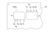
- FIG. 4 is a plan view showing the mounting positions of the first diode bridge 21Aa and the second diode bridge 21Ab on the printed wiring board 10.
- the first diode bridge 21Aa and the second diode bridge 21Ab are mounted on the printed wiring board 10 so that their respective terminal arrangement surfaces TS are aligned in a horizontal row.
- the first terminal T1 of the first diode bridge 21Aa and the fourth terminal T4 of the second diode bridge 21Ab are adjacent to each other, but the creepage distance X is ensured to be 3.2 mm or more. Therefore, a sufficient creepage distance is ensured.
- terminal groups TG of the first diode bridge 21Aa and the second diode bridge 21Ab do not face each other, heat is less likely to concentrate on each terminal and the conductive pattern to which each terminal is soldered.
- one of the inputs of the second converter 20B is connected to any one of the first wiring 11 (R phase), the second wiring 12 (S phase), and the third wiring 13 (T phase) between the input terminal 9 and the first converter 20A, and the other of the inputs of the second converter 20B is connected to the fourth wiring 14 (N phase).
- the branch point of the fifth wiring 15 is located between the center position of the length of the first wiring 11 from which the fifth wiring 15 branches and the input terminal 9. As a result, the branch point of the fifth wiring 15 is located away from the first converter 20A, and heat concentration around the terminals of the first converter 20A is suppressed.
- Each of the first diode bridge 21Aa and the second diode bridge 21Ab is a diode module in which four bridge-connected diode chips are built into one package.
- the two diode modules are mounted on the first surface 10a of the printed wiring board 10.
- the two diode modules are spaced apart so that their respective terminal groups TG have a creepage distance of 3.2 mm or more, and are arranged so that their respective terminal arrangement surfaces TS do not face each other. Therefore, the terminal groups of the two diode modules do not face each other, and heat concentration on the terminals and conductive patterns is suppressed.
- the diode module may also have a heat sink.
- a first varistor 28 serving as a surge absorber is connected between the AC input terminals of the first diode bridge 21Aa and the second diode bridge 21Ab, so that even if a voltage exceeding a predetermined value is applied between the AC input terminals, the voltage between the AC input terminals can be limited to a predetermined value.
- a second varistor 29 is connected between the DC output terminals of the first diode bridge 21Aa and the second diode bridge 21Ab, so that external pulses or power supply noise are absorbed and the transmission of noise to the AC power supply is also prevented.
- the first inverter circuit 25A and the second inverter circuit 25B are power modules in which upper arm switching elements and lower arm switching elements are built into a single package, and are mounted on the first surface 10 a of the printed wiring board 10 .
- Modularization makes it easier to design the peripheral circuits on the first surface 10a of the printed wiring board 10, which is the mounting surface.
- printed wiring board 10 is a multilayer printed wiring board having multiple conductive pattern layers stacked with insulating layers sandwiched between them, the conductive patterns can be wired not only on the surface of printed wiring board 10 but also on inner layers, allowing components to be mounted at a high density.
- FIG. 5 is a plan view showing the mounting positions of the first diode bridge 21Aa and the second diode bridge 21Ab on the printed wiring board 10 in a first modification.
- the first diode bridge 21Aa and the second diode bridge 21Ab are mounted on the printed wiring board 10 so that their respective terminal arrangement surfaces TS face in opposite directions.
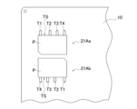
- FIG. 6 is a plan view showing the mounting positions of the first diode bridge 21Aa and the second diode bridge 21Ab on the printed wiring board 10 in a second modification.
- the first diode bridge 21Aa and the second diode bridge 21Ab are mounted on the printed wiring board 10 so that their terminal arrangement surfaces TS face in opposite directions and are aligned in a direction perpendicular to the arrangement direction of the terminal group TG.
- FIG. 7 is a plan view showing the mounting positions of the first diode bridge 21Aa and the second diode bridge 21Ab on the printed wiring board 10 in a third modification.
- the first diode bridge 21Aa and the second diode bridge 21Ab are mounted on the printed wiring board 10 so that their terminal arrangement surfaces TS face the same direction and are aligned in a direction perpendicular to the arrangement direction of the terminal group TG.
- Second Embodiment Fig. 8 is a circuit diagram showing a configuration of a power generating device 200 according to a second embodiment of the present disclosure.
- the difference from the power generating device 100 in Fig. 1 is that a third converter 20C is further provided. Since the other configurations are the same as those of the power generating device 100 in Fig. 1, only the differences will be described here.
- the third converter 20C includes a fourth diode bridge 21C and a third smoothing capacitor 22C.
- the fourth diode bridge 21C is connected between the sixth wiring 16 and the seventh wiring 17.
- the sixth wiring 16 and the seventh wiring 17 branch off from any two of the first wiring 11, the second wiring 12, and the third wiring 13. In this embodiment, the sixth wiring 16 branches off from the second wiring 12, and the seventh wiring 17 branches off from the third wiring 13.
- the third converter 20C converts AC power into DC power and supplies the DC power to a predetermined load (excluding the first inverter circuit 25A, the second inverter circuit 25B, the switching power supply 31, and the four-way switching valve circuit 32).
- a predetermined load excluding the first inverter circuit 25A, the second inverter circuit 25B, the switching power supply 31, and the four-way switching valve circuit 32.
- the DC power is supplied to the motor-operated valve drive circuit 33 as shown in FIG. 8.
- the motor-operated valve drive circuit 33 controls the operation of the motor-operated valve 63.
- each of the two inputs of the third converter 20C is connected to any two of the first wiring 11, second wiring 12, and third wiring 13 between the input terminal 9 and the first converter 20A, thereby suppressing an increase in the value of the current flowing through the first diode bridge 21Aa and second diode bridge 21Ab of the first converter 20A.
- the branch point of the sixth wiring 16 is located between the center position of the length of the second wiring 12 where the sixth wiring 16 branches off and the input terminal 9.
- the branch point of the seventh wiring 17 is located between the center position of the length of the third wiring 13 where the seventh wiring 17 branches off and the input terminal 9.
- the first diode bridge 21Aa is connected between the first wiring 11 and the second wiring 12
- the second diode bridge 21Ab is connected between the second wiring 12 and the third wiring 13.
- first diode bridge 21Aa may be connected between the second wiring 12 and the third wiring 13
- second diode bridge 21Ab may be connected between the first wiring 11 and the third wiring 13.
- first diode bridge 21Aa may be connected between the first wiring 11 and the third wiring 13
- second diode bridge 21Ab may be connected between the first wiring 11 and the second wiring 12.
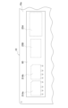
- FIG. 9 is a plan view of a heat sink 60 that cools the first diode bridge 21Aa, the second diode bridge 21Ab, the first inverter circuit 25A, and the second inverter circuit 25B.
- the first diode bridge 21Aa, the second diode bridge 21Ab, the first inverter circuit 25A, and the second inverter circuit 25B are high heat generating components.
- the first diode bridge 21Aa, the second diode bridge 21Ab, the first inverter circuit 25A, and the second inverter circuit 25B are mounted on the first surface 10a of the printed wiring board 10, so they can be cooled by a common heat sink 60. This allows for a reduction in the number of components and a reduction in the installation space.
- FIG. 10 is a circuit diagram showing the configuration of a power generating device 300 including a first diode bridge 21Aa connected to one power supply line selected from three power supply lines including the first wiring 11, the second wiring 12, and the third wiring 13, and a second diode bridge 21Ab connected between the remaining two power supply lines.
- the first converter 20A converts the three-phase AC power supply R (R phase), S (S phase), and T (T phase) into a DC power supply consisting of DC+ (positive pole) and DC- (negative pole), and supplies it to the inverter 25A.
- the first converter 20A includes a first diode bridge 21Aa, a second diode bridge 21Ab, and a first smoothing capacitor 22A.
- the first diode bridge 21Aa is a single-phase diode bridge.
- the first diode bridge 21Aa full-wave rectifies the AC power input from the first wiring 11 connected to the R phase and the branch wiring 11a branching off from the first wiring 11.
- the second diode bridge 21Ab is a single-phase diode bridge.
- the second diode bridge 21Ab full-wave rectifies the AC power input from the second wiring 12 and the third wiring 13 connected to the T phase.
- FIG. 10 is one example.
- the first diode bridge 21Aa may full-wave rectify the AC power input from the second wiring 12 connected to the S phase and the branch wiring branching off from the second wiring 12, and the second diode bridge 21Ab may full-wave rectify the AC power input from the first wiring 11 connected to the R phase and the third wiring 13 connected to the T phase.
- the first diode bridge 21Aa may full-wave rectify the AC power input from the third wiring 13 connected to the T phase and the branch wiring branching off from the third wiring 13, and the second diode bridge 21Ab may full-wave rectify the AC power input from the first wiring 11 connected to the R phase and the second wiring 12 connected to the S phase.
- the branch wiring 11a branching from the first wiring 11 as in FIG. 10 may be eliminated, and the first diode bridge 21Aa may simply be connected to the first wiring 11 as in the circuit diagram of a power generating device 300 shown in FIG.
Landscapes
- Engineering & Computer Science (AREA)
- Power Engineering (AREA)
- Inverter Devices (AREA)
Abstract
本開示の目的は、三相4線400Vの空調機に搭載される3相コンバータに替えて、2個の単相ダイオードブリッジが使用される場合において、単相ダイオードブリッジ自体およびその直下のパターンの発熱を抑制することである。電力生成装置(100)は、第1コンバータ(20A)および第2コンバータ(20B)を含み、それらはプリント配線板(10)に実装されている。第1コンバータ(20A)は、R相と繋がる第1配線(11)とS相に繋がる第2配線(12)との間に接続される第1ダイオードブリッジ(21Aa)、および第2配線(12)とT相に繋がる第3配線(13)との間に接続される第2ダイオードブリッジ(21Ab)を含み、交流電力を直流電力に変換する。第2コンバータ(20B)は、N相に繋がる第4配線(14)と第1配線(11)から分岐する第5配線(15)との間に接続される第3ダイオードブリッジ(21B)を含み、交流電力を直流電力に変換する。
Description
三相4線400Vの空調機に搭載される電力生成装置に関する。
三相4線400Vの空調機において、室外機に搭載された400V系コンバータ回路は、例えば、特許文献1(特開2012-165509号公報)に開示されているように、一般的には1個の三相ダイオードブリッジで構成される。
その一方で、高コスト化する三相ダイオードブリッジからの脱却を図るため、単相ダイオードブリッジの2個使いが検討されている。
しかしながら、三相4線400Vの空調機において、1個の三相ダイオードブリッジに替えて単相ダイオードブリッジの2個使いを適用するには、単相ダイオードブリッジ自体およびその直下のパターンの発熱を抑制する、という課題が存在する。
第1観点の電力生成装置は、プリント配線板に実装される電力生成装置であって、入力端子と、第1配線、第2配線、第3配線および第4配線と、第1コンバータと、第5配線と、第2コンバータとを備える。入力端子は、三相交流を三相4線式で供給する電源からR相、S相、T相およびN相が入力されるように構成される。第1配線、第2配線、第3配線および第4配線は、入力端子を介してR相、S相、T相およびN相それぞれと接続される。第1コンバータは、第1配線と第2配線と第3配線の3つの電源線から第1の組合せとして選択された2つの電源線の間に接続される第1ダイオードブリッジ、および当該3つの電源線から第1の組合せとは異なる第2の組合せとして選択された2つの電源線の間に接続される第2ダイオードブリッジを含み、交流電力を直流電力に変換する。第5配線は、第1配線、第2配線および第3配線のいずれか1つの配線から分岐する。第2コンバータは、第4配線と第5配線との間に接続される第3ダイオードブリッジを含み、交流電力を直流電力に変換する。
この電力生成装置では、第2コンバータの入力の一方が入力端子と第1コンバータとの間の第1配線、第2配線および第3配線のいずれか1つに接続され、第2コンバータの入力の他方が第4線(N相)に接続されているので、第1コンバータの第1ダイオードブリッジおよび第2ダイオードブリッジに流れる電流値の増大を抑制することができる。
第2観点の電力生成装置は、プリント配線板に実装される電力生成装置であって、入力端子と、第1配線、第2配線、第3配線および第4配線と、第1コンバータと、第5配線と、第2コンバータとを備える。入力端子は、三相交流を三相4線式で供給する電源からR相、S相、T相およびN相が入力されるように構成される。第1配線、第2配線、第3配線および第4配線は、入力端子を介してR相、S相、T相およびN相それぞれと接続される。第1コンバータは、第1配線と第2配線と第3配線の3つの電源線から選択された1つの電源線に接続される第1ダイオードブリッジ、および残り2つの電源線の間に接続される第2ダイオードブリッジを含み、交流電力を直流電力に変換する。第5配線は、第1配線、第2配線および第3配線のいずれか1つの配線から分岐する。第2コンバータは、第4配線と第5配線との間に接続される第3ダイオードブリッジを含み、交流電力を直流電力に変換する。
この電力生成装置では、第2コンバータの入力の一方が入力端子と第1コンバータとの間の第1配線、第2配線および第3配線のいずれか1つに接続され、第2コンバータの入力の他方が第4線(N相)に接続されているので、第1コンバータの第1ダイオードブリッジおよび第2ダイオードブリッジに流れる電流値の増大を抑制することができる。
第3観点の電力生成装置は、第1観点または第2観点の電力生成装置であって、第5配線の分岐点が、第5配線が分岐される配線の長さの中央位置と入力端子との間に位置する。
この電力生成装置では、第5配線の分岐点が、入力端子から第1コンバータまでの区間のうち、少なくとも当該区間の半分以上の距離を保って第1コンバータから離れている。このように、第5配線の分岐点を第1コンバータから遠ざけることによって、第5配線の分岐点における発熱が第1コンバータに伝導し難くなり、第1コンバータの端子周辺に熱が集中することが抑制される。
第4観点の電力生成装置は、第1観点から第3観点のいずれか1つの電力生成装置であって、第6配線および第7配線と、第3コンバータとさらに備える。第6配線および第7配線は、第1配線、第2配線および第3配線のいずれか2つの配線から分岐する。第3コンバータは、第6配線と第7配線との間に接続される第4ダイオードブリッジを含み、交流電力を直流電力に変換する。
この電力生成装置では、第3コンバータの2つの入力それぞれが、入力端子と第1コンバータとの間の第1配線、第2配線および第3配線のいずれか2つに接続されているので、第1コンバータの第1ダイオードブリッジおよび第2ダイオードブリッジに流れる電流値の増大を抑制することができる。
第5観点の電力生成装置は、第1観点から第4観点のいずれか1つの電力生成装置であって、第1ダイオードブリッジおよび第2ダイオードブリッジそれぞれが、ブリッジ接続された4つのダイオードチップが1つのパッケージに内蔵されているダイオードモジュールである。2つのダイオードモジュールは、プリント配線板の第1面に実装される。
第6観点の電力生成装置は、第5観点の電力生成装置であって、ダイオードモジュールが、端子群と、端子群が配置される端子配置面とを有する。端子群では、2つの交流入力端子と2つの直流出力端子とが第1方向に一列に並ぶ。2つのダイオードモジュールは、それぞれの端子群が互いに3.2mm以上の沿面距離となるように隔てられ、且つそれぞれの端子配置面が互いに対向しないように配置される。
この電力生成装置では、2つのダイオードモジュールそれぞれの端子群が向き合わないので、端子および導電パターンへの熱集中が抑制される。
第7観点の電力生成装置は、第5観点の電力生成装置であって、ダイオードモジュールが放熱板を有する。
第8観点の電力生成装置は、第5観点の電力生成装置であって、ダイオードモジュールが、2つの交流入力端子と2つの直流出力端子とを有している。2つの交流入力端子の間に、バリスタおよびサージアブソーバの少なくとも1つが接続される。
この電力生成装置では、交流入力端子間に所定値を超える電圧が掛かっても、交流入力端子間の電圧を所定値に制限することができる。
第9観点の電力生成装置は、第5観点の電力生成装置であって、ダイオードモジュールが、2つの交流入力端子と2つの直流出力端子とを有する。2つの直流出力端子の間に、バリスタおよびフィルムコンデンサの少なくとも1つが接続される。
この電力生成装置では、外来パルスが吸収され、或いは電源ノイズが吸収され、さらには交流電源へのノイズの伝送も防止される。
第10観点の電力生成装置は、第1観点から第9観点のいずれか1つの電力生成装置であって、第1コンバータの出力端子間に接続される第1インバータ回路をさらに備える。第1インバータ回路は、上アーム側スイッチング素子および下アーム側スイッチング素子が1つのパッケージに内蔵されたパワーモジュールであり、プリント配線板の第1面に実装される。
この電力生成装置では、モジュール化によって実装面であるプリント配線板の第1面における周辺回路の設計が容易になる。
第11観点の電力生成装置は、第1観点から第10観点のいずれか1つの電力生成装置であって、第2コンバータの出力端子間に接続される第2インバータ回路をさらに備える。第2インバータ回路は、上アーム側スイッチング素子および下アーム側スイッチング素子が1つのパッケージに内蔵されたパワーモジュールであり、プリント配線板の第1面に実装される。
この電力生成装置では、モジュール化によって実装面であるプリント配線板の第1面における周辺回路の設計が容易になる。
第12観点の電力生成装置は、第1観点から第11観点のいずれか1つの電力生成装置であって、プリント配線板が、絶縁体層を挟んで積層される複数の導電パターン層を有する多層プリント配線板である。
この電力生成装置では、導電パターンをプリント配線板の表面だけでなく、内層にも配線できるので、部品を高密度に実装することができる。
第13観点の電力生成装置は、第5観点の電力生成装置であって、第1インバータ回路と、第2インバータ回路と、1つのヒートシンクをさらに備える。第1インバータ回路は、第1コンバータの出力端子間に接続される。第2インバータ回路は、第2コンバータの出力端子間に接続される。第1インバータ回路および第2インバータ回路それぞれは、上アーム側スイッチング素子および下アーム側スイッチング素子が1つのパッケージに内蔵されたパワーモジュールであり、プリント配線板の第1面に実装される。ヒートシンクは、2つのダイオードモジュールと2つのパワーモジュールとを冷却する。
この電力生成装置では、1つのヒートシンクが、2つのダイオードモジュールと2つのパワーモジュールとを冷却するので、部品点数の削減、および設置スペースの削減を図ることができる。
<第1実施形態>
(1)電力生成装置100の概要
図1は、本開示の第1実施形態に係る電力生成装置100の構成を示す回路図である。図1において、電力生成装置100は、第1コンバータ20Aおよび第2コンバータ20Bを含み、それらはプリント配線板10の第1面10aに実装されている。
(1)電力生成装置100の概要
図1は、本開示の第1実施形態に係る電力生成装置100の構成を示す回路図である。図1において、電力生成装置100は、第1コンバータ20Aおよび第2コンバータ20Bを含み、それらはプリント配線板10の第1面10aに実装されている。
第1コンバータ20Aは、第1配線11と第2配線12と第3配線13の3つの電源線から第1の組合せとして選択された2つの電源線の間に接続される第1ダイオードブリッジ21Aa、および当該3つの電源線から第1の組合せとは異なる第2の組合せとして選択された2つの電源線の間に接続される第2ダイオードブリッジ21Abを含む。
本実施形態では、第1コンバータ20Aは、R相と繋がる第1配線11とS相に繋がる第2配線12との間に接続される第1ダイオードブリッジ21Aa、および第2配線12とT相に繋がる第3配線13との間に接続される第2ダイオードブリッジ21Abを含み、交流電力を直流電力に変換する。
第2コンバータ20Bは、N相に繋がる第4配線14と第1配線11から分岐する第5配線15との間に接続される第3ダイオードブリッジ21Bを含み、交流電力を直流電力に変換する。
本開示の電力生成装置100は、例えば、三相4線400Vの空調機の室外機に搭載される。
(2)詳細構成
(2-1)プリント配線板10
プリント配線板10は、絶縁体層を挟んで積層される複数の導電パターン層を有する多層プリント配線板である。
(2-1)プリント配線板10
プリント配線板10は、絶縁体層を挟んで積層される複数の導電パターン層を有する多層プリント配線板である。
プリント配線板10には、電力生成装置100の構成部品である、入力端子9、第1コンバータ20A、第2コンバータ20B、第1インバータ回路25A、第2インバータ回路25B、スイッチング電源31、四方切換弁回路32、それら構成部品を制御する複数のマイコンが実装されている。
入力端子9は、三相交流を三相4線式で供給する交流電源91からR相、S相、T相およびN相が入力されるように構成されている。導電パターンである第1配線11、第2配線12、第3配線13および第4配線14が、入力端子9を介して交流電源91のR相、S相、T相およびN相それぞれと接続されている。
(2-2)第1コンバータ20A
第1コンバータ20Aは、第1ダイオードブリッジ21Aa、第2ダイオードブリッジ21Abおよび第1平滑コンデンサ22Aを含む。
第1コンバータ20Aは、第1ダイオードブリッジ21Aa、第2ダイオードブリッジ21Abおよび第1平滑コンデンサ22Aを含む。
第1ダイオードブリッジ21Aaは、単相ダイオードブリッジである。第1ダイオードブリッジ21Aaは、R相と繋がる第1配線11と、S相に繋がる第2配線12とから入力される交流電力を全波整流する。
第2ダイオードブリッジ21Abは、単相ダイオードブリッジである。第2ダイオードブリッジ21Abは、第2配線12と、T相に繋がる第3配線13とから入力される交流電力を全波整流する。
第1ダイオードブリッジ21Aaおよび第2ダイオードブリッジ21Abは、ブリッジ接続された4つのダイオードチップが1つのパッケージに内蔵されているダイオードモジュールである。第1ダイオードブリッジ21Aaおよび第2ダイオードブリッジ21Abは、プリント配線板10の第1面10a上に実装される。
第1平滑コンデンサ22Aは、第1ダイオードブリッジ21Aaおよび第2ダイオードブリッジ21Abからの出力電圧を平滑化する。
(2-3)第2コンバータ20B
第2コンバータ20Bは、第3ダイオードブリッジ21B、および第2平滑コンデンサ22Bを含む。第3ダイオードブリッジ21Bは、単相ダイオードブリッジである。
第2コンバータ20Bは、第3ダイオードブリッジ21B、および第2平滑コンデンサ22Bを含む。第3ダイオードブリッジ21Bは、単相ダイオードブリッジである。
第3ダイオードブリッジ21Bは、N相に繋がる第4配線14と、第1配線11から分岐する第5配線15とから入力される交流電力を全波整流する。
第5配線15を分岐させる配線は、第1配線11、第2配線12および第3配線13のいずれでもよい。
第3ダイオードブリッジ21Bは、ブリッジ接続された4つのダイオードチップが1つのパッケージに内蔵されているダイオードモジュールである。
第2平滑コンデンサ22Bは、第3ダイオードブリッジ21Bからの出力電圧を平滑化する。
(2-4)電圧検出部23A
電圧検出部23Aは、第1平滑コンデンサ22Aの出力側に接続されており、第1平滑コンデンサ22Aの両端電圧を検出する。電圧検出部23Aは、互いに直列に接続された2つの抵抗が平滑コンデンサ22に並列接続され、第1平滑コンデンサ22Aの両端電圧が分圧されるように構成される。それら2つの抵抗同士の接続点の電圧値は、第1マイコン27Aに入力される。
電圧検出部23Aは、第1平滑コンデンサ22Aの出力側に接続されており、第1平滑コンデンサ22Aの両端電圧を検出する。電圧検出部23Aは、互いに直列に接続された2つの抵抗が平滑コンデンサ22に並列接続され、第1平滑コンデンサ22Aの両端電圧が分圧されるように構成される。それら2つの抵抗同士の接続点の電圧値は、第1マイコン27Aに入力される。
(2-5)電圧検出部23B
電圧検出部23Bは、第2平滑コンデンサ22Bの出力側に接続されており、第2平滑コンデンサ22Bの両端電圧を検出する。電圧検出部23Bは、互いに直列に接続された2つの抵抗が第2平滑コンデンサ22Bに並列接続され、第2平滑コンデンサ22Bの両端電圧が分圧されるように構成される。それら2つの抵抗同士の接続点の電圧値は、第2マイコン27Bに入力される。
電圧検出部23Bは、第2平滑コンデンサ22Bの出力側に接続されており、第2平滑コンデンサ22Bの両端電圧を検出する。電圧検出部23Bは、互いに直列に接続された2つの抵抗が第2平滑コンデンサ22Bに並列接続され、第2平滑コンデンサ22Bの両端電圧が分圧されるように構成される。それら2つの抵抗同士の接続点の電圧値は、第2マイコン27Bに入力される。
(2-6)電流検出部24A
電流検出部24Aは、第1平滑コンデンサ22Aおよび第1インバータ回路25Aの間であって、かつ第1平滑コンデンサ22Aの負側出力端子側に接続されている。電流検出部24Aは、第1モータ51Aの起動後、第1モータ51Aに流れるモータ電流を検出する。
電流検出部24Aは、第1平滑コンデンサ22Aおよび第1インバータ回路25Aの間であって、かつ第1平滑コンデンサ22Aの負側出力端子側に接続されている。電流検出部24Aは、第1モータ51Aの起動後、第1モータ51Aに流れるモータ電流を検出する。
電流検出部24Aは、シャント抵抗および該抵抗の両端の電圧を増幅させるオペアンプを用いた増幅回路で構成されてもよい。電流検出部24Aによって検出されたモータ電流は、第1マイコン27Aに入力される。
(2-7)電流検出部24B
電流検出部24Bは、第2平滑コンデンサ22Bおよび第2インバータ回路25Bの間であって、かつ第2平滑コンデンサ22Bの負側出力端子側に接続されている。電流検出部24Bは、第2モータ51Bの起動後、第2モータ51Bに流れるモータ電流を検出する。
電流検出部24Bは、第2平滑コンデンサ22Bおよび第2インバータ回路25Bの間であって、かつ第2平滑コンデンサ22Bの負側出力端子側に接続されている。電流検出部24Bは、第2モータ51Bの起動後、第2モータ51Bに流れるモータ電流を検出する。
電流検出部24Bは、シャント抵抗および該抵抗の両端の電圧を増幅させるオペアンプを用いた増幅回路で構成されてもよい。電流検出部24Bによって検出されたモータ電流は、第2マイコン27Bに入力される。
(2-8)第1インバータ回路25A、第2インバータ回路25B
第1インバータ回路25Aは、第1平滑コンデンサ22Aの出力側に接続される。第2インバータ回路25Bは、第2平滑コンデンサ22Bの出力側に接続される。第1インバータ回路25Aと第2インバータ回路25Bの構成は同じであるので、それらをインバータ回路25として説明する。
第1インバータ回路25Aは、第1平滑コンデンサ22Aの出力側に接続される。第2インバータ回路25Bは、第2平滑コンデンサ22Bの出力側に接続される。第1インバータ回路25Aと第2インバータ回路25Bの構成は同じであるので、それらをインバータ回路25として説明する。
図2は、インバータ回路25およびそれを駆動する駆動回路26の構成図である。図2において、インバータ回路25は、スイッチング素子として、複数の絶縁ゲート型バイポーラトランジスタ(以下、単にトランジスタという)Q3a,Q3b,Q4a,Q4b,Q5a,Q5b及び複数の還流用のダイオードD3a,D3b,D4a,D4b,D5a,D5bを含む。
トランジスタQ3aとQ3b、Q4aとQ4b、Q5aとQ5bは、それぞれ互いに直列に接続されており、各ダイオードD3a~D5bは、各トランジスタQ3a~Q5bに、トランジスタのコレクタ端子とダイオードのカソード端子が、また、トランジスタのエミッタ端子とダイオードのアノード端子が接続されるよう、並列接続されている。
インバータ回路25は、コンバータからの直流電圧が印加され、かつ駆動回路26により指示されたタイミングで各トランジスタQ3a~Q5bがオン・オフを行うことによって、モータを駆動する駆動電圧SU,SV,SWを生成する。この駆動電圧SU,SV,SWは、各トランジスタQ3aとQ3b、Q4aとQ4b、Q5aとQ5bの各接続点NU,NV,NWからモータに出力される。
第1インバータ回路25Aおよび第2インバータ回路25Bは、上アーム側スイッチング素子(Q3a,Q4a,Q5a,D3a,D4a,D5a)および下アーム側スイッチング素子(Q3b,Q4b,Q5b,D3b,D4b,D5b)が1つのパッケージに内蔵されたパワーモジュールである。
第1インバータ回路25Aおよび第2インバータ回路25Bは、プリント配線板10の第1面10a上に実装される。
(2-9)第1駆動回路26A、第2駆動回路26B
第1駆動回路26Aは、第1マイコン27Aからの駆動指令に基づき、第1インバータ回路25Aの各トランジスタQ3a~Q5bのオン・オフの状態を変化させる。第2駆動回路26Bは、第2マイコン27Bからの駆動指令に基づき、第2インバータ回路25Bの各トランジスタQ3a~Q5bのオン・オフの状態を変化させる。
第1駆動回路26Aは、第1マイコン27Aからの駆動指令に基づき、第1インバータ回路25Aの各トランジスタQ3a~Q5bのオン・オフの状態を変化させる。第2駆動回路26Bは、第2マイコン27Bからの駆動指令に基づき、第2インバータ回路25Bの各トランジスタQ3a~Q5bのオン・オフの状態を変化させる。
第1駆動回路26Aと第2駆動回路26Bの構成は同じであるので、それらを駆動回路26として説明する。
図2に示すように、駆動回路26は、マイコンによって決定されたデューティを有する駆動電圧SU,SV,SWがインバータ回路25からモータに出力されるように、各トランジスタQ3a~Q5bのゲートに印加するゲート制御電圧Gu,Gx,Gv,Gy,Gw,Gzを生成する。生成されたゲート制御電圧Gu,Gx,Gv,Gy,Gw,Gzは、それぞれのトランジスタQ3a~Q5bのゲート端子に印加される。
(2-10)第1マイコン27A、第2マイコン27B、第3マイコン40
第1マイコン27Aは、電圧検出部23A、電流検出部24A、および第1駆動回路26Aと接続されている。第1マイコン27Aは、第1駆動回路26Aを制御して第1モータ51Aを駆動させる。一例として、本実施形態では、第1モータ51Aは圧縮機の駆動モータとして使用される。
第1マイコン27Aは、電圧検出部23A、電流検出部24A、および第1駆動回路26Aと接続されている。第1マイコン27Aは、第1駆動回路26Aを制御して第1モータ51Aを駆動させる。一例として、本実施形態では、第1モータ51Aは圧縮機の駆動モータとして使用される。
第2マイコン27Bは、電圧検出部23B、電流検出部24B、および第2駆動回路26Bと接続されている。第2マイコン27Bは、第2駆動回路26Bを制御して第2モータ51Bを駆動させる。一例として、本実施形態では、第2モータ51Bは、送風機の駆動モータとして使用される。
第3マイコン40は、冷媒制御マイコンである。第3マイコン40は、例えば、空調機の電動膨張弁の開度を制御し、冷媒の蒸発温度、過熱度および過冷却度を調整する。
(2-11)第1バリスタ28、第2バリスタ29
第1ダイオードブリッジ21Aaおよび第2ダイオードブリッジ21Abの交流入力端子間には、過電圧抑制素子としてサージアブソーバまたはバリスタが接続される。本実施形態では、第1バリスタ28が接続されている。第1バリスタ28は、交流入力端子間に所定値を超える電圧が掛かったときに、交流入力端子間の電圧を所定値に制限する。
第1ダイオードブリッジ21Aaおよび第2ダイオードブリッジ21Abの交流入力端子間には、過電圧抑制素子としてサージアブソーバまたはバリスタが接続される。本実施形態では、第1バリスタ28が接続されている。第1バリスタ28は、交流入力端子間に所定値を超える電圧が掛かったときに、交流入力端子間の電圧を所定値に制限する。
また、第1ダイオードブリッジ21Aaおよび第2ダイオードブリッジ21Abの直流出力端子間には、過電圧抑制素子およびノイズ除去素子の少なくとも一方が接続される。過電圧抑制素子としては、サージアブソーバまたはバリスタが採用される。また、ノイズ除去素子としては、フィルムコンデンサが採用される。本実施形態では、過電圧抑制素子の第2バリスタ29が接続されている。第2バリスタ29は、第1平滑コンデンサ22Aと第1インバータ回路25Aとの間に接続され、スイッチング素子の動作時に生じるサージを吸収する。
(2-12)スイッチング電源31
スイッチング電源31は、第2コンバータ20Bの出力側に接続されており、第1マイコン27A、第2マイコン27Bおよび第3マイコン40に電力を供給する。
スイッチング電源31は、第2コンバータ20Bの出力側に接続されており、第1マイコン27A、第2マイコン27Bおよび第3マイコン40に電力を供給する。
(2-13)四方切換弁回路32
四方切換弁回路32は、第2コンバータ20Bの出力側に接続されている。四方切換弁回路32は、第2コンバータ20Bから出力される電力を利用して、四方切換弁61の流路を切り換える。四方切換弁61は、冷媒回路における冷媒の循環方向を切り換える弁である。
四方切換弁回路32は、第2コンバータ20Bの出力側に接続されている。四方切換弁回路32は、第2コンバータ20Bから出力される電力を利用して、四方切換弁61の流路を切り換える。四方切換弁61は、冷媒回路における冷媒の循環方向を切り換える弁である。
(3)第1コンバータ20Aと第2コンバータ20Bとの関係
本実施形態の第1コンバータ20Aは、三相4線式の交流電源の交流電力を2つの第1ダイオードブリッジ21Aaと第2ダイオードブリッジ21Abとで全波整流する回路構成であり、1つの三相ダイオードブリッジで全波整流する回路構成と比べてコストメリットがある。
本実施形態の第1コンバータ20Aは、三相4線式の交流電源の交流電力を2つの第1ダイオードブリッジ21Aaと第2ダイオードブリッジ21Abとで全波整流する回路構成であり、1つの三相ダイオードブリッジで全波整流する回路構成と比べてコストメリットがある。
他方、第1ダイオードブリッジ21Aaおよび第2ダイオードブリッジ21Abの単体の耐熱性は、1つの三相ダイオードブリッジのダイオードモジュールに比べて低いので、動作時の発熱対策が必要となる。
そこで、本実施形態では、第1ダイオードブリッジ21Aaおよび第2ダイオードブリッジ21Abそれぞれに流れる電流を低く抑えるため、スイッチング電源31および四方切換弁回路32の電源を第1コンバータ20Aの下流から取らない構成である。
具体的には、図1に示すように、第2コンバータ20Bに入力される交流電力は、N相に繋がる第4配線14と、R相に繋がる第1配線11から分岐した第5配線15とから入力される交流電力である。
その上で、スイッチング電源31および四方切換弁回路32の電源を第2コンバータ20Bの下流から取る。これによって、第1ダイオードブリッジ21Aaおよび第2ダイオードブリッジ21Abそれぞれに流れる電流の増大を抑えることができる。
また、第5配線15の分岐点は、第5配線15が分岐される第1配線11の長さの中央位置と入力端子9との間に位置する。具体的には、第5配線15の分岐点が、入力端子9から第1コンバータ20Aまでの区間のうち、少なくとも当該区間の半分以上の距離を保って第1コンバータ20Aから離れている。このように、第5配線15の分岐点を第1コンバータ20Aから遠ざけることによって、第5配線15の分岐点における発熱が第1コンバータ20Aに伝導し難くなり、第1ダイオードブリッジ21Aaおよび第2ダイオードブリッジ21Abの端子周辺に熱が集中することが抑制される。
(4)第1、第2ダイオードブリッジ21Aa,21Abの配置
図3Aと図3Bは、第1ダイオードブリッジ21Aa、第2ダイオードブリッジ21Abとして使用されるダイオードモジュール21の平面図と側面図である。図3Aおよび図3Bにおいて、ダイオードモジュール21は、ブリッジ接続された4つのダイオードチップを内蔵する直方体形状のパッケージPと、パッケージPの一側面から突出する端子群TGとを含む。
図3Aと図3Bは、第1ダイオードブリッジ21Aa、第2ダイオードブリッジ21Abとして使用されるダイオードモジュール21の平面図と側面図である。図3Aおよび図3Bにおいて、ダイオードモジュール21は、ブリッジ接続された4つのダイオードチップを内蔵する直方体形状のパッケージPと、パッケージPの一側面から突出する端子群TGとを含む。
端子群TGは、第1端子T1、第2端子T2、第3端子T3および第4端子T4を含む。端子群TGは、パッケージPの厚み方向に平行で且つ2つの長辺を含む2面のうちの1面から突出した後、直角に曲げられている。端子群TGが突出している面を端子配置面TSとする。
端子配置面TSと平行に対向する面側の1つのコーナーには傾斜面Cが形成されている。端子群TGは、傾斜面Cに最も近い第1端子T1を基準にして、第2端子T2、第3端子T3および第4端子T4が傾斜面Cから離れる方向(以下、第1方向D1という。)に順に並んでいる。
第2端子T2と第3端子T3は交流入力端子である。第1端子T1は正極の直流出力端子である。第4端子T4は、負極の直流出力端子である。
図4は、プリント配線板10上の第1ダイオードブリッジ21Aaおよび第2ダイオードブリッジ21Abの実装位置を示す平面図である。図4において、第1ダイオードブリッジ21Aaおよび第2ダイオードブリッジ21Abは、それぞれの端子配置面TSが横一列に並ぶようにプリント配線板10上に実装されている。
第1ダイオードブリッジ21Aaの第1端子T1と第2ダイオードブリッジ21Abの第4端子T4とが互いに隣接するが、沿面距離Xが3.2mm以上確保されている。それゆえ、十分な沿面距離が確保されている。
さらに、第1ダイオードブリッジ21Aaおよび第2ダイオードブリッジ21Ab双方の端子群TGが向かい合っていないので、各端子および各端子が半田付けされる導電パターンに熱が集中し難い。
(5)特徴
(5-1)
電力生成装置100では、第2コンバータ20Bの入力の一方が入力端子9と第1コンバータ20Aとの間の第1配線11(R相)、第2配線12(S相)および第3配線13(T相)のいずれか1つに接続され、第2コンバータ20Bの入力の他方が第4配線14(N相)に接続されている。その結果、第1コンバータ20Aの第1ダイオードブリッジ21Aaおよび第2ダイオードブリッジ21Abに流れる電流値の増大が抑制される。
(5-1)
電力生成装置100では、第2コンバータ20Bの入力の一方が入力端子9と第1コンバータ20Aとの間の第1配線11(R相)、第2配線12(S相)および第3配線13(T相)のいずれか1つに接続され、第2コンバータ20Bの入力の他方が第4配線14(N相)に接続されている。その結果、第1コンバータ20Aの第1ダイオードブリッジ21Aaおよび第2ダイオードブリッジ21Abに流れる電流値の増大が抑制される。
(5-2)
第5配線15の分岐点が、第5配線15が分岐される第1配線11の長さの中央位置と入力端子9との間に位置する。その結果、第5配線15の分岐点が第1コンバータ20Aから遠ざかり、第1コンバータ20Aの端子周辺に熱が集中することが抑制される。
第5配線15の分岐点が、第5配線15が分岐される第1配線11の長さの中央位置と入力端子9との間に位置する。その結果、第5配線15の分岐点が第1コンバータ20Aから遠ざかり、第1コンバータ20Aの端子周辺に熱が集中することが抑制される。
(5-3)
第1ダイオードブリッジ21Aaおよび第2ダイオードブリッジ21Abそれぞれは、ブリッジ接続された4つのダイオードチップが1つのパッケージに内蔵されているダイオードモジュールである。2つのダイオードモジュールは、プリント配線板10の第1面10a上に実装される。
第1ダイオードブリッジ21Aaおよび第2ダイオードブリッジ21Abそれぞれは、ブリッジ接続された4つのダイオードチップが1つのパッケージに内蔵されているダイオードモジュールである。2つのダイオードモジュールは、プリント配線板10の第1面10a上に実装される。
2つのダイオードモジュールは、それぞれの端子群TGが互いに3.2mm以上の沿面距離となるように隔てられ、且つそれぞれの端子配置面TSが互いに対向しないように配置される。それゆえ、2つのダイオードモジュールそれぞれの端子群が向き合わず、端子および導電パターンへの熱集中が抑制される。また、ダイオードモジュールが放熱板を有してもよい。
(5-4)
第1ダイオードブリッジ21Aaおよび第2ダイオードブリッジ21Abそれぞれの交流入力端子の間に、サージアブソーバとしての第1バリスタ28が接続されている。それゆえ、交流入力端子間に所定値を超える電圧が掛かっても、交流入力端子間の電圧を所定値に制限することができる。
第1ダイオードブリッジ21Aaおよび第2ダイオードブリッジ21Abそれぞれの交流入力端子の間に、サージアブソーバとしての第1バリスタ28が接続されている。それゆえ、交流入力端子間に所定値を超える電圧が掛かっても、交流入力端子間の電圧を所定値に制限することができる。
(5-5)
第1ダイオードブリッジ21Aaおよび第2ダイオードブリッジ21Abそれぞれの直流出力端子の間に、第2バリスタ29が接続されている。それゆえ、外来パルス、或いは電源ノイズが吸収され、さらには交流電源へのノイズの伝送も防止される。
第1ダイオードブリッジ21Aaおよび第2ダイオードブリッジ21Abそれぞれの直流出力端子の間に、第2バリスタ29が接続されている。それゆえ、外来パルス、或いは電源ノイズが吸収され、さらには交流電源へのノイズの伝送も防止される。
(5-6)
第1インバータ回路25Aおよび第2インバータ回路25Bは、上アーム側スイッチング素子および下アーム側スイッチング素子が1つのパッケージに内蔵されたパワーモジュールであり、プリント配線板10の第1面10a上に実装される。
第1インバータ回路25Aおよび第2インバータ回路25Bは、上アーム側スイッチング素子および下アーム側スイッチング素子が1つのパッケージに内蔵されたパワーモジュールであり、プリント配線板10の第1面10a上に実装される。
モジュール化によって実装面であるプリント配線板10の第1面10aにおける周辺回路の設計が容易になる。
(5-7)
プリント配線板10が、絶縁体層を挟んで積層される複数の導電パターン層を有する多層プリント配線板であるので、導電パターンをプリント配線板10の表面だけでなく、内層にも配線でき、部品を高密度に実装することができる。
プリント配線板10が、絶縁体層を挟んで積層される複数の導電パターン層を有する多層プリント配線板であるので、導電パターンをプリント配線板10の表面だけでなく、内層にも配線でき、部品を高密度に実装することができる。
(6)変形例
第1ダイオードブリッジ21Aaおよび第2ダイオードブリッジ21Abの配置は、図4の配置に限定されるものではないので、以下、変形例として説明する。
第1ダイオードブリッジ21Aaおよび第2ダイオードブリッジ21Abの配置は、図4の配置に限定されるものではないので、以下、変形例として説明する。
(6-1)第1変形例
図5は、第1変形例におけるプリント配線板10上の第1ダイオードブリッジ21Aaおよび第2ダイオードブリッジ21Abの実装位置を示す平面図である。
図5は、第1変形例におけるプリント配線板10上の第1ダイオードブリッジ21Aaおよび第2ダイオードブリッジ21Abの実装位置を示す平面図である。
図5において、第1ダイオードブリッジ21Aaおよび第2ダイオードブリッジ21Abは、それぞれの端子配置面TSが互いに反対方向を向くようにプリント配線板10上に実装されている。
第1ダイオードブリッジ21Aaの端子群TGと第2ダイオードブリッジ21Abの端子群TGとが向かい合っていないので、各端子および各端子が半田付けされる導電パターンに熱が集中し難い。
(6-2)第2変形例
図6は、第2変形例におけるプリント配線板10上の第1ダイオードブリッジ21Aaおよび第2ダイオードブリッジ21Abの実装位置を示す平面図である。
図6は、第2変形例におけるプリント配線板10上の第1ダイオードブリッジ21Aaおよび第2ダイオードブリッジ21Abの実装位置を示す平面図である。
図6において、第1ダイオードブリッジ21Aaおよび第2ダイオードブリッジ21Abは、それぞれの端子配置面TSが互いに反対方向を向き、且つ端子群TGの並び方向と直交する方向に並ぶように、プリント配線板10上に実装されている。
第1ダイオードブリッジ21Aaの端子群TGと第2ダイオードブリッジ21Abの端子群TGとが向かい合っていないので、各端子および各端子が半田付けされる導電パターンに熱が集中し難い。
(6-3)第3変形例
図7は、第3変形例におけるプリント配線板10上の第1ダイオードブリッジ21Aaおよび第2ダイオードブリッジ21Abの実装位置を示す平面図である。
図7は、第3変形例におけるプリント配線板10上の第1ダイオードブリッジ21Aaおよび第2ダイオードブリッジ21Abの実装位置を示す平面図である。
図7において、第1ダイオードブリッジ21Aaおよび第2ダイオードブリッジ21Abは、それぞれの端子配置面TSは互いに同一方向を向き、且つ端子群TGの並び方向と直交する方向に並ぶように、プリント配線板10上に実装されている。
第1ダイオードブリッジ21Aaの端子群TGと第2ダイオードブリッジ21Abの端子群TGとが向かい合っていないので、各端子および各端子が半田付けされる導電パターンに熱が集中し難い。
<第2実施形態>
図8は、本開示の第2実施形態に係る電力生成装置200の構成を示す回路図である。図8において、図1の電力生成装置100との違いは、第3コンバータ20Cをさらに備えている点である。他の構成は、図1の電力生成装置100と同じであるので、ここでは相違点についてのみ説明する。
図8は、本開示の第2実施形態に係る電力生成装置200の構成を示す回路図である。図8において、図1の電力生成装置100との違いは、第3コンバータ20Cをさらに備えている点である。他の構成は、図1の電力生成装置100と同じであるので、ここでは相違点についてのみ説明する。
第3コンバータ20Cは、第4ダイオードブリッジ21Cと第3平滑コンデンサ22Cとを含む。第4ダイオードブリッジ21Cは、第6配線16と第7配線17との間に接続されている。第6配線16および第7配線17は、第1配線11、第2配線12および第3配線13のいずれか2つの配線から分岐している。この実施形態では、第6配線16は第2配線12から分岐し、第7配線17は第3配線13から分岐している。
第3コンバータ20Cは、交流電力を直流電力に変換し、その直流電力を所定負荷(第1インバータ回路25A、第2インバータ回路25B、スイッチング電源31および四方切換弁回路32を除く)に供給する。一例として、本実施形態では、図8に示すように直流電力を電動弁駆動回路33に供給する。電動弁駆動回路33は、電動弁63の動作を制御する。
電力生成装置200では、第3コンバータ20Cの2つの入力それぞれが、入力端子9と第1コンバータ20Aとの間の第1配線11、第2配線12および第3配線13のいずれか2つに接続されており、それによって第1コンバータ20Aの第1ダイオードブリッジ21Aaおよび第2ダイオードブリッジ21Abに流れる電流値の増大を抑制している。
また、第6配線16の分岐点は、第6配線16が分岐される第2配線12の長さの中央位置と入力端子9との間に位置する。さらに、第7配線17の分岐点は、第7配線17が分岐される第3配線13の長さの中央位置と入力端子9との間に位置する。その結果、第6配線16および第7配線17の分岐点が第1コンバータ20Aから遠ざかり、第1コンバータ20Aの端子周辺に熱が集中することが抑制される。
<第1実施形態および第2実施形態に共通の変形例>
第1実施形態および第2実施形態では、第1ダイオードブリッジ21Aaが第1配線11と第2配線12との間に接続され、第2ダイオードブリッジ21Abが第2配線12と第3配線13との間に接続されている。
第1実施形態および第2実施形態では、第1ダイオードブリッジ21Aaが第1配線11と第2配線12との間に接続され、第2ダイオードブリッジ21Abが第2配線12と第3配線13との間に接続されている。
しかし、これに限定されるものではなく、第1ダイオードブリッジ21Aaが第2配線12と第3配線13との間に接続され、第2ダイオードブリッジ21Abが第1配線11と第3配線13との間に接続されてもよい。
或いは、第1ダイオードブリッジ21Aaが第1配線11と第3配線13との間に接続され、第2ダイオードブリッジ21Abが第1配線11と第2配線12との間に接続されてもよい。
<他の構成>
(A)
図9は、第1ダイオードブリッジ21Aa、第2ダイオードブリッジ21Ab、第1インバータ回路25Aおよび第2インバータ回路25Bを冷却するヒートシンク60の平面図である。
(A)
図9は、第1ダイオードブリッジ21Aa、第2ダイオードブリッジ21Ab、第1インバータ回路25Aおよび第2インバータ回路25Bを冷却するヒートシンク60の平面図である。
第1実施形態および第2実施形態において、第1ダイオードブリッジ21Aa、第2ダイオードブリッジ21Ab、第1インバータ回路25Aおよび第2インバータ回路25Bは、高発熱部品である。
図9において、第1ダイオードブリッジ21Aa、第2ダイオードブリッジ21Ab、第1インバータ回路25Aおよび第2インバータ回路25Bは、プリント配線板10の第1面10a上に実装されているので、共通のヒートシンク60でそれらを冷却することができる。それゆえ、部品点数の削減、および設置スペースの削減を図ることができる。
(B)
図10は、第1配線11と第2配線12と第3配線13の3つの電源線から選択された1つの電源線に接続される第1ダイオードブリッジ21Aa、および残り2つの電源線の間に接続される第2ダイオードブリッジ21Abを含む電力生成装置300の構成を示す回路図である。
図10は、第1配線11と第2配線12と第3配線13の3つの電源線から選択された1つの電源線に接続される第1ダイオードブリッジ21Aa、および残り2つの電源線の間に接続される第2ダイオードブリッジ21Abを含む電力生成装置300の構成を示す回路図である。
図10において、第1コンバータ20Aは、3相交流電源R(R相)、S(S相)、T(T相)をDC+(正極)及びDC-(負極)からなる直流電源に変換し、インバータ25Aに供給する。
第1コンバータ20Aは、第1ダイオードブリッジ21Aa、第2ダイオードブリッジ21Abおよび第1平滑コンデンサ22Aを含む。
図10では、第1ダイオードブリッジ21Aaは、単相ダイオードブリッジである。第1ダイオードブリッジ21Aaは、R相と繋がる第1配線11と、第1配線11から分岐する分岐配線11aとから入力される交流電力を全波整流する。
第2ダイオードブリッジ21Abは、単相ダイオードブリッジである。第2ダイオードブリッジ21Abは、第2配線12と、T相に繋がる第3配線13とから入力される交流電力を全波整流する。
図10と図1とは、電源線と第1ダイオードブリッジ21Aaとの結線方法が異なるだけで、それ以外の構成は同じであるので、説明は省略する。
図10は一例であり、他の例として、第1ダイオードブリッジ21AaがS相と繋がる第2配線12と、第2配線12から分岐する分岐配線とから入力される交流電力を全波整流し、第2ダイオードブリッジ21AbがR相に繋がる第1配線11と、T相に繋がる第3配線13とから入力される交流電力を全波整流してもよい。
或いは、第1ダイオードブリッジ21AaがT相と繋がる第3配線13と、第3配線13から分岐する分岐配線とから入力される交流電力を全波整流し、第2ダイオードブリッジ21AbがR相に繋がる第1配線11と、S相に繋がる第2配線12とから入力される交流電力を全波整流してもよい。
(C)
但し、図10のような第1配線11から分岐する分岐配線11aを廃止して、図11に示す電力生成装置300の回路図ように、第1ダイオードブリッジ21Aaは第1配線11と繋がるだけでもよい。
但し、図10のような第1配線11から分岐する分岐配線11aを廃止して、図11に示す電力生成装置300の回路図ように、第1ダイオードブリッジ21Aaは第1配線11と繋がるだけでもよい。
(D)
図10に示す、電源線と第1ダイオードブリッジ21Aaとの結線方法を図8に適用して、図12に示す電力生成装置400の回路図ように構成することもできる。
図10に示す、電源線と第1ダイオードブリッジ21Aaとの結線方法を図8に適用して、図12に示す電力生成装置400の回路図ように構成することもできる。
(E)
図11に示す、電源線と第1ダイオードブリッジ21Aaの結線方法を図8に適用して、図13に示す電力生成装置400の回路図ように構成することもできる。
図11に示す、電源線と第1ダイオードブリッジ21Aaの結線方法を図8に適用して、図13に示す電力生成装置400の回路図ように構成することもできる。
以上、本開示の実施形態を説明したが、特許請求の範囲に記載された本開示の趣旨および範囲から逸脱することなく、形態や詳細の多様な変更が可能なことが理解されるであろう。
9 入力端子
10 プリント配線板
10a 第1面
11 第1配線
12 第2配線
13 第3配線
14 第4配線
15 第5配線
16 第6配線
17 第7配線
20A 第1コンバータ
20B 第2コンバータ
20C 第3コンバータ
21Aa 第1ダイオードブリッジ
21Ab 第2ダイオードブリッジ
21B 第3ダイオードブリッジ
21C 第4ダイオードブリッジ
25A 第1インバータ回路
25B 第2インバータ回路
28 第1バリスタ
29 第2バリスタ
60 ヒートシンク
100、200 電力生成装置
300、400 電力生成装置
D3a、D4a、D5a 上アーム側スイッチング素子
D3b、D4b、D5b 下アーム側スイッチング素子
Q3a、Q4a、Q5a 上アーム側スイッチング素子
Q3b、Q4b、Q5b 下アーム側スイッチング素子
T1、T4 直流出力端子
T2、T3 交流入力端子
TG 端子群
TS 端子配置面
10 プリント配線板
10a 第1面
11 第1配線
12 第2配線
13 第3配線
14 第4配線
15 第5配線
16 第6配線
17 第7配線
20A 第1コンバータ
20B 第2コンバータ
20C 第3コンバータ
21Aa 第1ダイオードブリッジ
21Ab 第2ダイオードブリッジ
21B 第3ダイオードブリッジ
21C 第4ダイオードブリッジ
25A 第1インバータ回路
25B 第2インバータ回路
28 第1バリスタ
29 第2バリスタ
60 ヒートシンク
100、200 電力生成装置
300、400 電力生成装置
D3a、D4a、D5a 上アーム側スイッチング素子
D3b、D4b、D5b 下アーム側スイッチング素子
Q3a、Q4a、Q5a 上アーム側スイッチング素子
Q3b、Q4b、Q5b 下アーム側スイッチング素子
T1、T4 直流出力端子
T2、T3 交流入力端子
TG 端子群
TS 端子配置面
Claims (13)
- プリント配線板(10)に実装される電力生成装置であって、
三相交流を三相4線式で供給する電源からR相、S相、T相およびN相が入力されるように構成された入力端子(9)と、
前記入力端子(9)を介して前記R相、前記S相、前記T相および前記N相それぞれと接続される第1配線(11)、第2配線(12)、第3配線(13)および第4配線(14)と、
前記第1配線(11)と前記第2配線(12)と前記第3配線(13)の3つの電源線から第1の組合せとして選択された2つの前記電源線の間に接続される第1ダイオードブリッジ(21Aa)、および3つの前記電源線から前記第1の組合せとは異なる第2の組合せとして選択された2つの前記電源線の間に接続される第2ダイオードブリッジ(21Ab)を含み、交流電力を直流電力に変換する第1コンバータ(20A)と、
前記第1配線(11)、前記第2配線(12)および前記第3配線(13)のいずれか1つの配線から分岐する第5配線(15)と、
前記第4配線(14)と前記第5配線(15)との間に接続される第3ダイオードブリッジ(21B)を含み、交流電力を直流電力に変換する第2コンバータ(20B)と、
を備える、
電力生成装置(100,200)。 - プリント配線板(10)に実装される電力生成装置であって、
三相交流を三相4線式で供給する電源からR相、S相、T相およびN相が入力されるように構成された入力端子(9)と、
前記入力端子(9)を介して前記R相、前記S相、前記T相および前記N相それぞれと接続される第1配線(11)、第2配線(12)、第3配線(13)および第4配線(14)と、
前記第1配線(11)と前記第2配線(12)と前記第3配線(13)の3つの電源線から選択された1つの前記電源線に接続される第1ダイオードブリッジ(21Aa)、および残り2つの前記電源線の間に接続される第2ダイオードブリッジ(21Ab)を含み、交流電力を直流電力に変換する第1コンバータ(20A)と、
前記第1配線(11)、前記第2配線(12)および前記第3配線(13)のいずれか1つの配線から分岐する第5配線(15)と、
前記第4配線(14)と前記第5配線(15)との間に接続される第3ダイオードブリッジ(21B)を含み、交流電力を直流電力に変換する第2コンバータ(20B)と、
を備える、
電力生成装置(300,400)。 - 前記第5配線(15)の分岐点は、前記第5配線(15)が分岐される前記配線の長さの中央位置と前記入力端子(9)との間に位置する、
請求項1または請求項2に記載の電力生成装置(100,200,300,400)。 - 前記第1配線(11)、前記第2配線(12)および前記第3配線(13)のいずれか2つの配線から分岐する第6配線(16)および第7配線(17)と、
前記第6配線(16)と前記第7配線(17)との間に接続される第4ダイオードブリッジ(21C)を含み、交流電力を直流電力に変換する第3コンバータ(20C)と、
をさらに備える、
請求項1から請求項3のいずれか1項に記載の電力生成装置(200,400)。 - 前記第1ダイオードブリッジ(21Aa)および前記第2ダイオードブリッジ(21Ab)それぞれは、ブリッジ接続された4つのダイオードチップが1つのパッケージに内蔵されているダイオードモジュールであり、2つの前記ダイオードモジュールが前記プリント配線板(10)の第1面(10a)に実装される、
請求項1から請求項4のいずれか1項に記載の電力生成装置(100,200,300,400)。 - 前記ダイオードモジュールは、
2つの交流入力端子(T2,T3)と2つの直流出力端子(T1,T4)とが第1方向に一列に並ぶ端子群(TG)と、
前記端子群(TG)が配置される端子配置面(TS)と、
を有し、
2つの前記ダイオードモジュールは、それぞれの前記端子群(TG)が互いに3.2mm以上の沿面距離となるように隔てられ、且つそれぞれの前記端子配置面(TS)が互いに対向しないように配置される、
請求項5に記載の電力生成装置(100,200,300,400)。 - 前記ダイオードモジュールは、放熱板を有する、
請求項5に記載の電力生成装置(100,200,300,400)。 - 前記ダイオードモジュールは、2つの交流入力端子と2つの直流出力端子とを有し、
2つの前記交流入力端子(T2,T3)の間に、過電圧抑制素子が接続される、
請求項5に記載の電力生成装置(100,200,300,400)。 - 前記ダイオードモジュールは、2つの交流入力端子(T2,T3)と2つの直流出力端子(T1,T4)とを有し、
2つの前記直流出力端子(T1,T4)の間に、過電圧抑制素子およびノイズ除去素子の少なくとも1つが接続される、
請求項5に記載の電力生成装置(100,200,300,400)。 - 前記第1コンバータ(20A)の出力端子間に接続される第1インバータ回路(25A)をさらに備え、
前記第1インバータ回路(25A)は、上アーム側スイッチング素子(Q3a,Q4a,Q5a,D3a,D4a,D5a)および下アーム側スイッチング素子(Q3b,Q4b,Q5b,D3b,D4b,D5b)が1つのパッケージに内蔵されたパワーモジュールであり、前記プリント配線板(10)の第1面(10a)に実装される、
請求項1から請求項9のいずれか1項に記載の電力生成装置(100,200,300,400)。 - 前記第2コンバータ(20B)の出力端子間に接続される第2インバータ回路(25B)をさらに備え、
前記第2インバータ回路(25B)は、上アーム側スイッチング素子(Q3a,Q4a,Q5a,D3a,D4a,D5a)および下アーム側スイッチング素子(Q3b,Q4b,Q5b,D3b,D4b,D5b)が1つのパッケージに内蔵されたパワーモジュールであり、前記プリント配線板(10)の第1面(10a)に実装される、
請求項1から請求項10のいずれか1項に記載の電力生成装置(100,200,300,400)。 - 前記プリント配線板(10)は、絶縁体層を挟んで積層される複数の導電パターン層を有する多層プリント配線板である、
請求項1から請求項11のいずれか1項に記載の電力生成装置(100,200,300,400)。 - 前記第1コンバータ(20A)の出力端子間に接続される第1インバータ回路(25A)と、
前記第2コンバータ(20B)の出力端子間に接続される第2インバータ回路(25B)と、
1つのヒートシンク(60)と、
をさらに備え、
前記第1インバータ回路(25A)および前記第2インバータ回路(25B)それぞれは、上アーム側スイッチング素子および下アーム側スイッチング素子が1つのパッケージに内蔵されたパワーモジュールであり、前記プリント配線板(10)の第1面(10a)に実装され、
前記ヒートシンク(60)が、2つの前記ダイオードモジュールと2つの前記パワーモジュールとを冷却する、
請求項5に記載の電力生成装置(100,200,300,400)。
Priority Applications (1)
| Application Number | Priority Date | Filing Date | Title |
|---|---|---|---|
| EP24828723.7A EP4597818A4 (en) | 2023-11-07 | 2024-10-24 | ENERGY GENERATION DEVICE |
Applications Claiming Priority (2)
| Application Number | Priority Date | Filing Date | Title |
|---|---|---|---|
| JP2023-189931 | 2023-11-07 | ||
| JP2023189931 | 2023-11-07 |
Publications (1)
| Publication Number | Publication Date |
|---|---|
| WO2025100245A1 true WO2025100245A1 (ja) | 2025-05-15 |
Family
ID=94382804
Family Applications (1)
| Application Number | Title | Priority Date | Filing Date |
|---|---|---|---|
| PCT/JP2024/037861 Pending WO2025100245A1 (ja) | 2023-11-07 | 2024-10-24 | 電力生成装置 |
Country Status (2)
| Country | Link |
|---|---|
| EP (1) | EP4597818A4 (ja) |
| WO (1) | WO2025100245A1 (ja) |
Citations (11)
| Publication number | Priority date | Publication date | Assignee | Title |
|---|---|---|---|---|
| JP2003319676A (ja) * | 2002-04-23 | 2003-11-07 | Hitachi Home & Life Solutions Inc | 電動機駆動装置 |
| JP2005033911A (ja) * | 2003-07-11 | 2005-02-03 | Sanken Electric Co Ltd | 3相交流−直流電力変換装置 |
| WO2007080748A1 (ja) * | 2006-01-16 | 2007-07-19 | Mitsubishi Electric Corporation | 電動機の駆動回路及び空気調和機の室外機 |
| JP2009148016A (ja) * | 2007-12-12 | 2009-07-02 | Panasonic Corp | 共用プリント基板およびそれを用いた直流電源回路 |
| JP2010112585A (ja) * | 2008-11-04 | 2010-05-20 | Daikin Ind Ltd | ヒートポンプ装置 |
| JP2012165509A (ja) | 2011-02-04 | 2012-08-30 | Panasonic Corp | 電力供給装置の突入電流防止回路 |
| JP2016073000A (ja) * | 2014-09-26 | 2016-05-09 | ローム株式会社 | 電源装置 |
| WO2018123521A1 (ja) * | 2016-12-27 | 2018-07-05 | 株式会社キトー | 三相・単相交流電源対応型電動巻上機 |
| JP2020096424A (ja) * | 2018-12-11 | 2020-06-18 | 東芝キヤリア株式会社 | 冷凍サイクル装置 |
| JP2021162234A (ja) * | 2020-03-31 | 2021-10-11 | ダイキン工業株式会社 | ヒートポンプ装置 |
| JP2022011145A (ja) * | 2020-06-29 | 2022-01-17 | ダイキン工業株式会社 | インバータ装置 |
Family Cites Families (5)
| Publication number | Priority date | Publication date | Assignee | Title |
|---|---|---|---|---|
| DE2238635A1 (de) * | 1972-08-05 | 1974-02-21 | Eltro Gmbh | Verfahren zur gewinnung einer gleichspannung |
| JP5766363B2 (ja) * | 2012-10-19 | 2015-08-19 | 株式会社ミツバ | 2相整流回路システム、及び発電機システム |
| CN204090301U (zh) * | 2014-07-11 | 2015-01-07 | 邯郸美的制冷设备有限公司 | 抗干扰pcb板及空调设备 |
| CN106128926B (zh) * | 2016-08-24 | 2018-03-09 | 南京普爱医疗设备股份有限公司 | 一种宽电源输入x射线管旋转阳极驱动装置及控制旋转阳极的方法 |
| CN219801908U (zh) * | 2022-12-29 | 2023-10-03 | 深圳科士达新能源有限公司 | 一种市电软启母线电路及并离网储能机 |
-
2024
- 2024-10-24 WO PCT/JP2024/037861 patent/WO2025100245A1/ja active Pending
- 2024-10-24 EP EP24828723.7A patent/EP4597818A4/en active Pending
Patent Citations (11)
| Publication number | Priority date | Publication date | Assignee | Title |
|---|---|---|---|---|
| JP2003319676A (ja) * | 2002-04-23 | 2003-11-07 | Hitachi Home & Life Solutions Inc | 電動機駆動装置 |
| JP2005033911A (ja) * | 2003-07-11 | 2005-02-03 | Sanken Electric Co Ltd | 3相交流−直流電力変換装置 |
| WO2007080748A1 (ja) * | 2006-01-16 | 2007-07-19 | Mitsubishi Electric Corporation | 電動機の駆動回路及び空気調和機の室外機 |
| JP2009148016A (ja) * | 2007-12-12 | 2009-07-02 | Panasonic Corp | 共用プリント基板およびそれを用いた直流電源回路 |
| JP2010112585A (ja) * | 2008-11-04 | 2010-05-20 | Daikin Ind Ltd | ヒートポンプ装置 |
| JP2012165509A (ja) | 2011-02-04 | 2012-08-30 | Panasonic Corp | 電力供給装置の突入電流防止回路 |
| JP2016073000A (ja) * | 2014-09-26 | 2016-05-09 | ローム株式会社 | 電源装置 |
| WO2018123521A1 (ja) * | 2016-12-27 | 2018-07-05 | 株式会社キトー | 三相・単相交流電源対応型電動巻上機 |
| JP2020096424A (ja) * | 2018-12-11 | 2020-06-18 | 東芝キヤリア株式会社 | 冷凍サイクル装置 |
| JP2021162234A (ja) * | 2020-03-31 | 2021-10-11 | ダイキン工業株式会社 | ヒートポンプ装置 |
| JP2022011145A (ja) * | 2020-06-29 | 2022-01-17 | ダイキン工業株式会社 | インバータ装置 |
Non-Patent Citations (1)
| Title |
|---|
| See also references of EP4597818A4 |
Also Published As
| Publication number | Publication date |
|---|---|
| EP4597818A1 (en) | 2025-08-06 |
| EP4597818A4 (en) | 2025-12-31 |
Similar Documents
| Publication | Publication Date | Title |
|---|---|---|
| US6791854B2 (en) | Semiconductor apparatus, power converter and automobile | |
| JP5094805B2 (ja) | 電圧検出装置及びそれを用いた電力変換装置 | |
| JP6901639B1 (ja) | 電力変換ユニット | |
| JP2019110228A (ja) | 電力変換装置 | |
| JP5354144B2 (ja) | インバータ | |
| KR101086577B1 (ko) | 교환가능한 셀을 포함하는 전력 전달 시스템 | |
| JP2012157138A (ja) | 電力変換装置のスタック構造 | |
| US20090195066A1 (en) | Power converter | |
| EP4597818A1 (en) | Power generation device | |
| JP2009229133A (ja) | 集積回路、半導体装置、電気機器 | |
| JPH1094256A (ja) | 電力変換素子モジュール | |
| US12627241B2 (en) | Semiconductor device having switching elements with two different current capacities | |
| WO2019043886A1 (ja) | 電力変換装置 | |
| CN111342686A (zh) | 功率变换装置及具备该功率变换装置的冷冻循环装置 | |
| US20250096079A1 (en) | Semiconductor Device and Inverter Provided With Semiconductor Device | |
| JP4424918B2 (ja) | 電力変換装置 | |
| JP2025098814A (ja) | 電源制御回路、およびそれを備えた空調機 | |
| JP3614704B2 (ja) | 電力変換装置 | |
| JPH07236281A (ja) | 電力変換装置 | |
| JP3275132B2 (ja) | 電力変換器 | |
| JP2022057179A (ja) | 電力変換装置 | |
| JP4828170B2 (ja) | 電力変換装置 | |
| JP6469837B2 (ja) | 電力変換ユニットおよび電力変換装置 | |
| JP2005057864A (ja) | 半導体モジュールとその使用方法 | |
| CN103312185B (zh) | 电源转换装置 |
Legal Events
| Date | Code | Title | Description |
|---|---|---|---|
| ENP | Entry into the national phase |
Ref document number: 2024828723 Country of ref document: EP Effective date: 20250108 |
|
| WWP | Wipo information: published in national office |
Ref document number: 2024828723 Country of ref document: EP |