CN100362702C - Tab terminal - Google Patents
Tab terminal Download PDFInfo
- Publication number
- CN100362702C CN100362702C CNB2004100434030A CN200410043403A CN100362702C CN 100362702 C CN100362702 C CN 100362702C CN B2004100434030 A CNB2004100434030 A CN B2004100434030A CN 200410043403 A CN200410043403 A CN 200410043403A CN 100362702 C CN100362702 C CN 100362702C
- Authority
- CN
- China
- Prior art keywords
- contact pin
- pin terminals
- circuit board
- printed circuit
- contact
- Prior art date
- Legal status (The legal status is an assumption and is not a legal conclusion. Google has not performed a legal analysis and makes no representation as to the accuracy of the status listed.)
- Expired - Fee Related
Links
- 238000003466 welding Methods 0.000 claims description 13
- 239000004020 conductor Substances 0.000 claims description 7
- 238000010521 absorption reaction Methods 0.000 description 2
- 238000007689 inspection Methods 0.000 description 2
- RYGMFSIKBFXOCR-UHFFFAOYSA-N Copper Chemical compound [Cu] RYGMFSIKBFXOCR-UHFFFAOYSA-N 0.000 description 1
- 238000010276 construction Methods 0.000 description 1
- 229910052802 copper Inorganic materials 0.000 description 1
- 239000010949 copper Substances 0.000 description 1
- 238000005516 engineering process Methods 0.000 description 1
- 238000009434 installation Methods 0.000 description 1
- 238000012986 modification Methods 0.000 description 1
- 230000004048 modification Effects 0.000 description 1
- 238000004080 punching Methods 0.000 description 1
- 239000000758 substrate Substances 0.000 description 1
Images

Classifications
-
- H—ELECTRICITY
- H01—ELECTRIC ELEMENTS
- H01R—ELECTRICALLY-CONDUCTIVE CONNECTIONS; STRUCTURAL ASSOCIATIONS OF A PLURALITY OF MUTUALLY-INSULATED ELECTRICAL CONNECTING ELEMENTS; COUPLING DEVICES; CURRENT COLLECTORS
- H01R13/00—Details of coupling devices of the kinds covered by groups H01R12/70 or H01R24/00 - H01R33/00
- H01R13/02—Contact members
- H01R13/04—Pins or blades for co-operation with sockets
- H01R13/05—Resilient pins or blades
- H01R13/055—Resilient pins or blades co-operating with sockets having a rectangular transverse section
-
- H—ELECTRICITY
- H01—ELECTRIC ELEMENTS
- H01R—ELECTRICALLY-CONDUCTIVE CONNECTIONS; STRUCTURAL ASSOCIATIONS OF A PLURALITY OF MUTUALLY-INSULATED ELECTRICAL CONNECTING ELEMENTS; COUPLING DEVICES; CURRENT COLLECTORS
- H01R13/00—Details of coupling devices of the kinds covered by groups H01R12/70 or H01R24/00 - H01R33/00
- H01R13/02—Contact members
- H01R13/10—Sockets for co-operation with pins or blades
- H01R13/11—Resilient sockets
- H01R13/115—U-shaped sockets having inwardly bent legs, e.g. spade type
-
- H—ELECTRICITY
- H01—ELECTRIC ELEMENTS
- H01R—ELECTRICALLY-CONDUCTIVE CONNECTIONS; STRUCTURAL ASSOCIATIONS OF A PLURALITY OF MUTUALLY-INSULATED ELECTRICAL CONNECTING ELEMENTS; COUPLING DEVICES; CURRENT COLLECTORS
- H01R43/00—Apparatus or processes specially adapted for manufacturing, assembling, maintaining, or repairing of line connectors or current collectors or for joining electric conductors
- H01R43/02—Apparatus or processes specially adapted for manufacturing, assembling, maintaining, or repairing of line connectors or current collectors or for joining electric conductors for soldered or welded connections
- H01R43/0256—Apparatus or processes specially adapted for manufacturing, assembling, maintaining, or repairing of line connectors or current collectors or for joining electric conductors for soldered or welded connections for soldering or welding connectors to a printed circuit board
Landscapes
- Coupling Device And Connection With Printed Circuit (AREA)
- Multi-Conductor Connections (AREA)
- Connections Effected By Soldering, Adhesion, Or Permanent Deformation (AREA)
Abstract
A tab terminal (1), capable of being mounted in a parts mounting space on a printed circuit board which is small in height, includes a terminal body (1a), an extension portion (1b) formed integrally with the terminal body so as to extend from one end edge of the terminal body in the longitudinal direction thereof, side wall portions (1d) formed integrally with the terminal body so as to extend from side edges of the terminal body in the height direction of the tab terminal, respectively, and contact portions (1e) formed integrally with the side wall portions so as to extend from distal end edges of the side wall portions in substantially parallel to the terminal body, respectively. The extension portion is adapted to be connected with an electrical connecting part, and the tab terminal is fixedly connected at the contact portions to the printed circuit board.
Description
Technical field
The present invention relates to a kind of contact pin terminals that are installed on the printed circuit board (PCB).
Background technology
In electric equipment, use printed circuit board (PCB) widely, this plate is formed with a conductor fig, and various circuit elements are installed on this plate.What also be installed on printed substrate is contact pin terminals, utilizes these contact pin terminals that conductor fig is linked to each other with an external circuit.Usually, the contact pin terminals comprise contact portion that is welded in conductor fig and an assembled portion of assembling socket terminals.By a lead these socket terminals are connected in external circuit (consulting JP-A-2002-324606).
Above-mentioned traditional contact pin terminals are designed to be installed on the printed circuit board (PCB) in such mode, and promptly it extends from a Surface Vertical of this printed circuit board (PCB), makes the height dimension of the part installing space on printed circuit board (PCB) bigger like this.In addition, as mentioned above, the socket terminals are assembled to the assembled portion of contact pin terminals and lead is connected in the contact pin terminals, therefore, require element installing space on printed circuit board (PCB) to have at least a height dimension greater than the total length of the terminals of contact pin terminals and socket.Be configured to the equipment of a multistage pattern with regard to printed circuit board (PCB), if printed circuit board (PCB) requires the bigger part installing space of a height dimension, the distance between so all printed circuit board (PCB)s must increase.Because these reasons, the size of the equipment of being made up of one or more circuit board that traditional contact pin terminals are installed becomes bigger.In addition, traditional contact pin terminals are configured to be installed on the printed circuit board (PCB) with its all time shank that inserts in all holes that are formed in the printed circuit board (PCB).Therefore, the contact pin terminals are troubles to a fitting operation of printed circuit board (PCB), and utilize the program of the automatic installation requirement complexity of erector.
Summary of the invention
A purpose of the present invention provides a kind of contact pin terminals that can be installed in the part installing space on the printed circuit board (PCB), that it is highly less.
According to the present invention, a kind of contact pin terminals that are suitable for being installed on the printed circuit board (PCB) are provided, these contact pin terminals comprise: a tabular contact pin terminals body; With the integrally formed extension of contact pin terminals body, make this part from an end limit of contact pin terminals body, along the longitudinal extension of contact pin terminals body, this extension is suitable for being connected with an electrical fitting; With integrally formed first and second sidewall sections of contact pin terminals body, make this two side respectively from the relative side of contact pin terminals body, extend along the short transverse of contact pin terminals; And with integrally formed first and second contact portions of first and second sidewall sections, make this two contact portion respectively from the distal edge of first and second sidewall sections, be basically parallel to the contact pin terminals and extend noumenally, the contact pin terminals are fixedly connected to printed circuit board (PCB) in the first and second contact site offices.
In the present invention, first and second contact portions can be configured to respectively extend with an angle smaller than the right angle with respect to first and second sidewall sections.The extension of contact pin terminals can be formed, and makes socket terminals that play the electrical fitting effect be assemblied in this extension.First and second contact portions can be soldered to the welding portion that is formed on the conductor fig in the printed circuit board (PCB).Contact pin terminals body can be formed with a picked part, and for example the pickup apparatus of a suction nozzle of an erector can arrive this picked part.First and second sidewall sections can have a height dimension, so that on a surface of the printed circuit board (PCB) that the contact pin terminals are installed be connected between the adjacently situated surfaces of electrical fitting of extension of contact pin terminals and form a gap.
Contact pin terminals of the present invention are fixedly connected to printed circuit board (PCB) in such mode in its first and second contact site offices, be that extend along printed circuit board (PCB) contact pin terminals body and extension, so that separate a distance corresponding to the height dimension of first and second sidewall sections with printed circuit board (PCB).Then, for example an electrical fitting of socket terminals is connected in the extension of contact pin terminals.In this mode, contact pin terminals of the present invention are installed on printed circuit board (PCB), and along its extension, as long as and the electrical fitting that is connected in the extension of contact pin terminals do not disturb mutually with the printed circuit board (PCB) that the contact pin terminals are installed, just can do the height dimension (sizes of its first and second sidewall sections) of contact pin terminals less.Therefore, compare, can reduce the height of contact pin terminals and the height dimension of part installing space with the vertical traditional contact pin terminals that are installed on printed circuit board (PCB).In addition, the extension of the contact pin terminals of connection electrical fitting is along the longitudinal extension of contact pin terminals body, and therefore, the electrical fitting that is connected in the extension also extends along printed circuit board (PCB).In this mode, according to contact pin terminals of the present invention, along printed circuit board (PCB) electrical fitting is set, therefore, and compares the height dimension that can reduce the part installing space on printed circuit board (PCB) significantly with respect to the vertical situation that electrical fitting is set of printed circuit board (PCB).This help with the size of the electric equipment of one or more printed circuit board construction dwindle, especially attenuation.
For according to preferred embodiment, the contact pin terminals that extend with an angle that is slightly less than the right angle with respect to first and second sidewall sections respectively of first and second contact portions wherein, when when assigning to by the weld part that first and second contact portions is welded in printed circuit board (PCB) the contact pin terminals being fixedly connected to printed circuit board (PCB), the scolder of welderingization enters in the gap between all surfaces of all contact portions and all welding portions fully.This guarantees that the contact pin terminals are fixedly connected to printed circuit board (PCB) reliably.
Be formed with the preferred embodiment of picked part according to contact pin terminals wherein, can enough erectors with this contact pin terminals mounted on surface in printed circuit board (PCB), thereby improved the efficient of fitting operation.
The accompanying drawing summary
From following only with illustrate, because of rather than limit detailed description and the accompanying drawing that mode of the present invention is narrated, the present invention will be understood more completely, in the accompanying drawings:
Fig. 1 is a stereogram that illustrates according to contact pin terminals of one embodiment of the invention;
Fig. 2 is a plane graph of contact pin terminals shown in Figure 1;
Fig. 3 is an end view of these contact pin terminals;
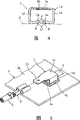
Fig. 4 is a front view of these contact pin terminals; And
Fig. 5 illustrates these contact pin terminals by a stereogram of this contact pin terminals of mounted on surface in a state of a printed circuit board (PCB).
Embodiment
In the following description, with contact pin terminals of explaining in detail according to one embodiment of the invention.
Shown in Fig. 1 to 4, the contact pin terminals 1 of this embodiment comprise a tabular contact pin terminals body 1a, from the end limit of contact pin terminals body 1a, along an extension 1b of the longitudinal extension of contact pin terminals body 1a, first and second sidewall sections 1d that extend from the relative side of contact pin terminals body 1a, along the short transverse of contact pin terminals 1 respectively; And respectively from all distal edge of all sidewall sections 1d, be basically parallel to the first and second contact portion 1e that contact pin terminals body 1a extends.Extension 1b, all sidewall sections 1d and all contact portion 1e and contact pin terminals body 1a are whole to be formed.By punching press have the electric conductivity of about 0.5 millimeter thickness splendid and be easy to a die-cut sheet copper and make contact pin terminals 1.
As shown in Figure 5, contact pin terminals 1 are mounted on the printed circuit board (PCB) 3.The contact pin terminals body 1a of contact pin terminals 1 is formed with a picked part 1h, thereby has the erector that part is picked up in an inspection for example a suction nozzle, that can arrive quilt absorption part 1h by use, contact pin terminals 1 can be installed on printed circuit board (PCB) 3.
Printed circuit board (PCB) 3 has a surperficial 3a who is formed with a conductor fig 4, and this conductor fig comprises welding portion 4a.Contact pin terminals 1 are welded in all welding portion 4a of printed circuit board (PCB) 3 at its first and second contact portion 1e places, thereby contact pin terminals 1 are fixedly connected to printed circuit board (PCB) 3.The first and second contact portion 1e are configured to make their distal surface that one spacing is arranged mutually.These contact portions 1e forms an angle that is slightly less than the right angle with respect to the first and second sidewall sections 1d respectively.More specifically, when the first and second contact portion 1e being placed on all welding portion 4a of printed circuit board (PCB) 3, the small angle theta diagonally extending that the outer surface of contact portion 13 (contact surface) 1f spends with a direction of leaving all welding portions about 10 with respect to the surface (representing with symbol S in Fig. 4) of all welding portion 4a, thus a wedge gap g between the surperficial S of all contact surface 1f and all welding portion 4a, formed.
In this embodiment, extension 1b is with the longitudinal extension of the state concordant with contact pin terminals body 1a along contact pin terminals body 1a, and as illustrated in fig. 1 and 2, wherein label 1c represents the upper surface of contact pin terminals body 1a.As shown in Figure 5, extension 1b is formed has the narrow width than contact pin terminals body 1a, this extension also has the terminal 1g of a chamfering, and be positioned in the predetermined height of all relatively contact portion 1e, thereby can be easy to be assembled to reliably extension 1b as a socket 5 of an electrical fitting.In this connected, the first and second sidewall sections 1d of contact pin terminals 1 had permission at a basal surface of the socket terminals 5 of the extension 1b that is assembled to contact pin terminals 1 with a height that forms a gap between the surperficial 3a of printed circuit board (PCB) 3 of contact pin terminals 1 is installed on it.One end of one lead 6 is clamped by socket terminals 5 and is connected, and the other end of lead 6 is connected in an external circuit (not shown).
The absorption inspection of an erector (not shown) by having a suction nozzle, the picked part 1h that relies on it is picked up contact pin terminals 1 with said structure and is transmitted towards printed circuit board (PCB) 3.Then, as shown in Figure 5, contact pin terminals 1 are placed on the printing electroplax 3, and all contact portion 1e align with all welding portion 4a of printed circuit board (PCB) 3 respectively.Simultaneously, the extension (assembled portion) of contact pin terminals 1 is arranged to leave and be parallel to the surperficial 3a of printed circuit board (PCB) 1.
Then, all contact portion 1e with contact pin terminals 1 are welded in all welding portion 4a.At this moment, all contact surface 1f of all contact portion 1e extend with a small angle theta with respect to the surperficial S of all welding portion 4a, form wedge gap g, therefore, the scolder of fusing enters this wedge gap g fully, thereby all contact portions are welded to all welding portion 4a reliably.Like this, contact pin terminals 1 are surface mounted on the printed circuit board (PCB) 3.After this, socket terminals 5 are connected to with assembling extension (assembled portion) 1b of contact pin terminals 1.
Because assembled portion 1b is configured to be parallel to the surperficial 3a of printed circuit board (PCB) 3, so socket terminals 5 are configured to be parallel to printed circuit board (PCB) 3.Thereby, contact pin terminals 1 can be installed in the part installing space on the printed circuit board (PCB) 3, that height dimension is less.In other words, can reduce the height dimension of the part installing space on printed circuit board (PCB).This can dwindle the size of electric equipment and attenuation it.
The present invention is not limited to the foregoing description, and various modifications can be arranged.
For example, although the contact pin terminals of this embodiment have its extension that is configured to socket terminals assemblings, the electrical fitting except the socket terminals can be connected to this extension.It is not necessarily required with an erector contact pin terminals being mounted to printed circuit board (PCB).
Claims (6)
1. contact pin terminals that are fit to be installed on the printed circuit board (PCB), it comprises:
One tabular contact pin terminals body;
With the integrally formed extension of contact pin terminals body, make this extension from an end limit of contact pin terminals body, along the longitudinal extension of contact pin terminals body, this extension is fit to be connected with an electrical fitting;
With integrally formed first and second sidewall sections of contact pin terminals body, make this two side respectively from the relative side of contact pin terminals body, extend along the short transverse of contact pin terminals; And
With integrally formed first and second contact portions of first and second sidewall sections, make this two contact portion respectively from the distal edge of first and second sidewall sections, be basically parallel to the contact pin terminals and extend noumenally, described first and second contact portions are extended with an angle that is slightly less than the right angle with respect to described first and second sidewall sections respectively, and these contact pin terminals are fixedly connected to printed circuit board (PCB) in the first and second contact site offices.
2. according to the contact pin terminals of claim 1, it is characterized in that: described first and second contact portions are extended on aspectant direction and a spacing are arranged therebetween.
3. according to the contact pin terminals of claim 1, it is characterized in that: the described extension of contact pin terminals forms, and can use the socket terminals as electrical fitting to be assembled to described extension.
4. according to the contact pin terminals of claim 1, it is characterized in that: described first and second contact portions are welded to the welding portion that is formed on the conductor fig in the printed circuit board (PCB) respectively.
5. according to the contact pin terminals of claim 1, it is characterized in that: described contact pin terminals are formed with a pickup apparatus accessibility one picked part of an erector.
6. according to the contact pin terminals of claim 1, it is characterized in that: described first and second sidewall sections have a height dimension, so that on a surface of the printed circuit board (PCB) that the contact pin terminals are installed be connected between the adjacently situated surfaces of electrical fitting of extension of contact pin terminals and form a gap.
Applications Claiming Priority (2)
| Application Number | Priority Date | Filing Date | Title |
|---|---|---|---|
| JP2003123943 | 2003-04-28 | ||
| JP2003123943A JP4274528B2 (en) | 2003-04-28 | 2003-04-28 | Tab terminal |
Publications (2)
| Publication Number | Publication Date |
|---|---|
| CN1543013A CN1543013A (en) | 2004-11-03 |
| CN100362702C true CN100362702C (en) | 2008-01-16 |
Family
ID=32985564
Family Applications (1)
| Application Number | Title | Priority Date | Filing Date |
|---|---|---|---|
| CNB2004100434030A Expired - Fee Related CN100362702C (en) | 2003-04-28 | 2004-04-26 | Tab terminal |
Country Status (5)
| Country | Link |
|---|---|
| US (1) | US7128623B2 (en) |
| EP (1) | EP1473802B1 (en) |
| JP (1) | JP4274528B2 (en) |
| CN (1) | CN100362702C (en) |
| DE (1) | DE602004001163T2 (en) |
Families Citing this family (17)
| Publication number | Priority date | Publication date | Assignee | Title |
|---|---|---|---|---|
| US8659158B2 (en) | 2006-08-16 | 2014-02-25 | Funai Electric Co., Ltd. | Thermally inkjettable acrylic dielectric ink formulation and process |
| KR101350972B1 (en) * | 2007-05-18 | 2014-01-14 | 엘지디스플레이 주식회사 | Backlight unit and liquid crystal display device module including the same |
| WO2009046752A1 (en) * | 2007-10-02 | 2009-04-16 | Osram Gesellschaft mit beschränkter Haftung | Plug device, plug connector, and method for producing the plug connector |
| US7766665B2 (en) * | 2008-01-31 | 2010-08-03 | Ivus Industries, Inc. | Printed circuit board direct connection and method of forming the same |
| CN101950866B (en) * | 2009-07-10 | 2014-03-05 | 深圳富泰宏精密工业有限公司 | Elastic sheet structure and electronic device applying same |
| JP5683284B2 (en) * | 2011-01-14 | 2015-03-11 | 矢崎総業株式会社 | Board connection terminal |
| DE102011017787A1 (en) | 2011-04-29 | 2012-10-31 | Robert Bosch Gmbh | Contact element for direct electrical contacting of printed circuit boards |
| JP6017129B2 (en) * | 2011-10-14 | 2016-10-26 | 日本圧着端子製造株式会社 | Connecting terminal |
| JP6063334B2 (en) * | 2013-04-19 | 2017-01-18 | 矢崎総業株式会社 | Terminal parts |
| KR200478327Y1 (en) | 2013-11-13 | 2015-09-30 | 한국단자공업 주식회사 | Terminal and terminal assembly |
| CN105981167B (en) * | 2014-08-12 | 2019-05-28 | 富士电机株式会社 | semiconductor device |
| JP6540398B2 (en) * | 2015-09-08 | 2019-07-10 | 株式会社オートネットワーク技術研究所 | Circuit structure |
| GB2537702C (en) * | 2015-10-22 | 2021-09-08 | Strip Tinning Ltd | Connectors |
| DE102016125897B4 (en) * | 2016-02-11 | 2022-06-23 | Few Fahrzeugelektrikwerk Gmbh & Co. Kg | Solderable electrical connection element |
| FR3084970B1 (en) * | 2018-08-13 | 2021-12-10 | Valeo Siemens Eautomotive France Sas | ELECTRICAL EQUIPMENT |
| BE1028071B1 (en) * | 2020-02-19 | 2021-09-13 | Phoenix Contact Gmbh & Co | Electrical contact element |
| USD1108377S1 (en) * | 2024-07-29 | 2026-01-06 | Yazaki Corporation | Terminal fitting for electric connector |
Citations (2)
| Publication number | Priority date | Publication date | Assignee | Title |
|---|---|---|---|---|
| US4332430A (en) * | 1979-10-26 | 1982-06-01 | Rockwell International Corporation | Printed circuit board connector |
| US6398559B2 (en) * | 1999-05-07 | 2002-06-04 | Kyoshin Kogyo Co., Ltd. | Connecting terminal and a connecting terminal assembly |
Family Cites Families (11)
| Publication number | Priority date | Publication date | Assignee | Title |
|---|---|---|---|---|
| GB1191629A (en) * | 1966-09-30 | 1970-05-13 | Lucas Industries Ltd | Fuse Holders |
| US4037898A (en) * | 1972-08-28 | 1977-07-26 | Beckman Instruments, Inc. | Snap-in electrical terminals |
| US4299436A (en) * | 1980-02-06 | 1981-11-10 | Universal Instruments Corporation | Electrical connector |
| US4873615A (en) * | 1986-10-09 | 1989-10-10 | Amp Incorporated | Semiconductor chip carrier system |
| JPH01140580A (en) * | 1987-11-25 | 1989-06-01 | Mitsubishi Electric Corp | Connection jumper and manufacture thereof |
| JPH0217818A (en) * | 1988-07-05 | 1990-01-22 | Yazaki Corp | electrical junction box |
| DE9017883U1 (en) * | 1990-08-31 | 1992-11-05 | Caradon Esser GmbH, 41469 Neuss | Contact element for SMD-assembled circuit boards |
| JP3395908B2 (en) | 1991-09-03 | 2003-04-14 | アンプ インコーポレイテッド | SMT type DIN connector |
| US5192228A (en) * | 1991-09-16 | 1993-03-09 | Amp Inc. | Shielded surface mount electrical connector with integral barbed board lock |
| DE9302836U1 (en) * | 1993-02-26 | 1993-07-22 | Siemens AG, 80333 München | Connectors |
| EP0887884B1 (en) * | 1997-05-28 | 2003-04-02 | Autonetworks Technologies, Ltd. | Bus bar structure |
-
2003
- 2003-04-28 JP JP2003123943A patent/JP4274528B2/en not_active Expired - Fee Related
-
2004
- 2004-03-19 US US10/803,959 patent/US7128623B2/en not_active Expired - Lifetime
- 2004-04-23 DE DE602004001163T patent/DE602004001163T2/en not_active Expired - Fee Related
- 2004-04-23 EP EP04009652A patent/EP1473802B1/en not_active Expired - Lifetime
- 2004-04-26 CN CNB2004100434030A patent/CN100362702C/en not_active Expired - Fee Related
Patent Citations (2)
| Publication number | Priority date | Publication date | Assignee | Title |
|---|---|---|---|---|
| US4332430A (en) * | 1979-10-26 | 1982-06-01 | Rockwell International Corporation | Printed circuit board connector |
| US6398559B2 (en) * | 1999-05-07 | 2002-06-04 | Kyoshin Kogyo Co., Ltd. | Connecting terminal and a connecting terminal assembly |
Also Published As
| Publication number | Publication date |
|---|---|
| JP4274528B2 (en) | 2009-06-10 |
| US20040214480A1 (en) | 2004-10-28 |
| JP2004327380A (en) | 2004-11-18 |
| US7128623B2 (en) | 2006-10-31 |
| CN1543013A (en) | 2004-11-03 |
| DE602004001163T2 (en) | 2007-05-31 |
| DE602004001163D1 (en) | 2006-07-27 |
| EP1473802B1 (en) | 2006-06-14 |
| EP1473802A1 (en) | 2004-11-03 |
Similar Documents
| Publication | Publication Date | Title |
|---|---|---|
| CN100362702C (en) | Tab terminal | |
| US7957156B2 (en) | Busbar circuit board assembly | |
| US8840408B2 (en) | Crank-shaped board terminal with a protruding support portion | |
| US7864544B2 (en) | Printed circuit board assembly | |
| US6244876B1 (en) | Busbar laminate assembly | |
| US7267556B2 (en) | Electrical junction box | |
| US7101197B2 (en) | Press-fit terminal, printed board connection structure using the press-fit terminal, and electrical connection box | |
| CN216698775U (en) | Electrical contact for connecting substrates together and electrical assembly including same | |
| CN101516162A (en) | Method and device for connecting circuit boards | |
| US20060166526A1 (en) | Double printed circuit board with solderless connecting structure | |
| EP1122825B1 (en) | Substrate mount type terminal | |
| US7841860B1 (en) | Compensating circuit board connector | |
| CN105322330B (en) | Double thickness both-end public affairs blade terminals | |
| US7591654B2 (en) | Conductor connecting module for printed circuit boards | |
| JP4586745B2 (en) | Terminal mounting structure on board | |
| JP2000077120A (en) | Connector terminal structure | |
| CN103765684A (en) | Assembly of plug connector and circuit board | |
| KR200227957Y1 (en) | A printed circuit board stacked junction box having connecting terminal | |
| TWM250339U (en) | Electrical connector with board lock | |
| EP1758208B1 (en) | A connector and a mounting method therefor | |
| KR102399767B1 (en) | Sub-pcb, pcb assembly including the same, and electronic devices using the same | |
| JP2012134086A (en) | Electric connection box | |
| CN1747244A (en) | PCB style headers using surface mount and through-hole packaging technologies | |
| US12308725B2 (en) | Modular circuit board arrangement and method for assembling a circuit board arrangement | |
| CN214477988U (en) | SMD socket |
Legal Events
| Date | Code | Title | Description |
|---|---|---|---|
| C06 | Publication | ||
| PB01 | Publication | ||
| C10 | Entry into substantive examination | ||
| SE01 | Entry into force of request for substantive examination | ||
| C14 | Grant of patent or utility model | ||
| GR01 | Patent grant | ||
| CF01 | Termination of patent right due to non-payment of annual fee |
Granted publication date: 20080116 Termination date: 20200426 |
|
| CF01 | Termination of patent right due to non-payment of annual fee |