CN100367464C - Method for manufacturing metal bump - Google Patents
Method for manufacturing metal bump Download PDFInfo
- Publication number
- CN100367464C CN100367464C CNB2005100624203A CN200510062420A CN100367464C CN 100367464 C CN100367464 C CN 100367464C CN B2005100624203 A CNB2005100624203 A CN B2005100624203A CN 200510062420 A CN200510062420 A CN 200510062420A CN 100367464 C CN100367464 C CN 100367464C
- Authority
- CN
- China
- Prior art keywords
- metal
- layer
- substrate
- protective layer
- bonding pad
- Prior art date
- Legal status (The legal status is an assumption and is not a legal conclusion. Google has not performed a legal analysis and makes no representation as to the accuracy of the status listed.)
- Expired - Fee Related
Links
Images


Classifications
-
- H—ELECTRICITY
- H10—SEMICONDUCTOR DEVICES; ELECTRIC SOLID-STATE DEVICES NOT OTHERWISE PROVIDED FOR
- H10W—GENERIC PACKAGES, INTERCONNECTIONS, CONNECTORS OR OTHER CONSTRUCTIONAL DETAILS OF DEVICES COVERED BY CLASS H10
- H10W72/00—Interconnections or connectors in packages
- H10W72/01—Manufacture or treatment
- H10W72/012—Manufacture or treatment of bump connectors, dummy bumps or thermal bumps
Landscapes
- Exposure And Positioning Against Photoresist Photosensitive Materials (AREA)
Abstract
Description
技术领域technical field
本发明涉及一种制造金属凸块的方法,尤其是涉及一种可以改善金属凸块周缘阶跃高度和增加封装品质的方法。The invention relates to a method for manufacturing a metal bump, in particular to a method which can improve the step height of the metal bump periphery and increase the packaging quality.
背景技术Background technique
随着便携式电子器材的发展,各种轻、薄、短小的封装体不断地被开发出来,倒装片球面格栅阵列(BGA)封装体就是其中一例。在倒装片BGA封装体中,管芯(die)不再是将接合垫金属(bonding pad)经由丝焊连接到封装基板上,而是反转过来通过金凸块或导电聚合物凸块等连接到封装基板上,因此倒装片BGA封装体可提升电路密度和提升电气特性。With the development of portable electronic devices, various light, thin, and short packages are continuously developed, and the flip-chip ball grid array (BGA) package is one example. In a flip-chip BGA package, the die (die) is no longer connected to the package substrate by bonding the pad metal (bonding pad) via wire bonding, but is reversed through gold bumps or conductive polymer bumps, etc. Connected to the package substrate, so the flip-chip BGA package can increase circuit density and improve electrical characteristics.
倒装片接合属于区域阵列式的接合,因此能应用于极高密度的构装。简单来说,倒装片接合的观念是先在管芯的接合垫金属上长成金属凸块,然后可利用如各向异性导电胶膜(ACF)或银胶等,将金属凸块黏附在封装基板上,进而完成管芯与封装基板的接合。这种方式不仅可突破传统打线技术的数目限制,并适合多脚数元件封装,而且电性效能也因具有较短的连接通路而大幅度提高。Flip-chip bonding belongs to area array bonding, so it can be applied to extremely high-density packaging. To put it simply, the concept of flip-chip bonding is to first grow metal bumps on the bonding pad metal of the die, and then use such as anisotropic conductive film (ACF) or silver glue to adhere the metal bumps to the chip. on the packaging substrate, and then complete the bonding of the die and the packaging substrate. This method not only breaks through the limitation of the number of traditional wire bonding technology, but also is suitable for multi-pin component packaging, and the electrical performance is also greatly improved due to the shorter connection path.
参照图1,图1为公知的金属凸块20与封装基板22接合的示意图。如图1所示,一管芯10表面包括有至少一接合垫金属12、一氧化层14、一氮化硅16。其中,氧化层14和氮化硅16为一保护层18且依次堆叠在管芯10表面,并覆盖在部分接合垫金属12表面。另外,在管芯10上方还具有一金属凸块20,因为保护层18在接合垫金属12周缘上方具有一阶跃高度,因此金属凸块20形成后,其周缘也会具有一相对应的阶跃高度。这样,当金属凸块20与一封装基板22进行接合时,因为金属凸块20的周缘所具有的阶跃高度,便非常容易地使得部分涂覆于金属凸块20与封装基板22界面间的各向异性导电胶膜24不能确实地将金属凸块20与封装基板22接合。Referring to FIG. 1 , FIG. 1 is a schematic diagram of a
由上述可知,金属凸块20周缘的阶跃高度如果过大,会严重地影响到封装的质量,然而如果没有金属凸块20周缘的阶跃高度,各向异性导电胶膜24不能妥善的被聚集于金属凸块20表面。公知的技术通常是利用两种方法来改善此问题,第一种方法是将保护层18沉积的厚度变薄,然而该方法将大幅度降低产品的可靠性。第二种方法则是将接合垫金属12缩小,然而此方法将使得压合的面积缩小而导致各向异性导电胶膜24不够均匀。It can be seen from the above that if the step height of the
发明内容Contents of the invention
因此,本发明的主要目的在于提供一种制造金属凸块的方法,以解决上述的问题。Therefore, the main objective of the present invention is to provide a method for manufacturing metal bumps to solve the above-mentioned problems.
为达到上述目的,根据本发明的优选实施例,本发明首先提供一基底,基底表面包括有一图案化保护层暴露出至少一个接合垫金属的部分表面,接着形成一光阻层覆盖于基底表面,然后利用一光掩模进行一光刻处理过程将光阻层图案化,以暴露出部分保护层和接合垫金属,接着移除部分保护层,使得覆盖在接合垫金属表面的保护层的厚度小于覆盖在基底表面的保护层的厚度,最后移除光阻层并利用光掩模进行一金属凸块化处理过程。In order to achieve the above object, according to a preferred embodiment of the present invention, the present invention firstly provides a substrate, the surface of the substrate includes a patterned protective layer exposing a part of the surface of at least one bonding pad metal, and then a photoresist layer is formed to cover the surface of the substrate, Then use a photomask to perform a photolithography process to pattern the photoresist layer to expose part of the protective layer and the bonding pad metal, and then remove part of the protective layer so that the thickness of the protective layer covering the surface of the bonding pad metal is less than The thickness of the protective layer covering the surface of the substrate is finally removed and a metal bumping process is performed using a photomask.
由于本发明可以有效改善金属凸块周缘的阶跃高度,经由本发明使得金属凸块周缘的阶跃高度缩小,将更有利于提高金属凸块与封装基板之间的接合效果,进而大幅度提高封装的质量。另外,本发明在制造处理过程中,可以不需要增加额外的光掩模,因此也不需要增加光掩模的成本。Since the present invention can effectively improve the step height of the periphery of the metal bump, the reduction of the step height of the periphery of the metal bump through the present invention will be more conducive to improving the bonding effect between the metal bump and the packaging substrate, thereby greatly improving the The quality of the package. In addition, the present invention does not need to add an additional photomask during the manufacturing process, and therefore does not need to increase the cost of the photomask.
为使本发明的目的、特征和优点能更明显易于理解,下面特举优选实施例,并配合附图做详细说明。然而附图仅用于参考和辅助说明,并非用来对本发明加以限制。In order to make the purpose, features and advantages of the present invention more obvious and easy to understand, preferred embodiments are specifically cited below and described in detail with accompanying drawings. However, the drawings are only for reference and auxiliary description, and are not used to limit the present invention.
附图说明Description of drawings
图1为公知金属凸块与封装基板接合的示意图;FIG. 1 is a schematic diagram of a conventional metal bump bonded to a package substrate;
图2至图7为根据本发明第一实施例的制造金属凸块的方法示意图;2 to 7 are schematic diagrams of a method for manufacturing a metal bump according to a first embodiment of the present invention;
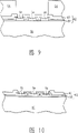
图8至图10为根据本发明第二实施例的制造金属凸块的方法示意图。8 to 10 are schematic diagrams of a method for manufacturing a metal bump according to a second embodiment of the present invention.
具体实施方式Detailed ways
参照图2至图7,图2至图7为根据本发明第一实施例的制造金属凸块48的方法示意图。如图2所示,首先提供一基底30,基底30可以是一完成内部元件与线路制作的芯片或完成内部线路布局的多层印刷电路板等。基底30表面包括有至少一接合垫金属32、一氧化层34以及一氮化硅36。其中,接合垫金属32为铝构成,另外氧化层34与氮化硅36结合构成一图案化保护层38,保护层38覆盖在部分接合垫金属32表面并暴露出接合垫金属32的部分表面。氧化层34和氮化硅36分别通过沉积处理过程同时形成在基底30和接合垫金属32表面。本实施例中,氧化层34和氮化硅36所构成的保护层38在基底30和接合垫金属32表面所形成的厚度大约相同。Referring to FIG. 2 to FIG. 7 , FIG. 2 to FIG. 7 are schematic diagrams of a method for manufacturing the
如图3所示,接着利用旋涂的方法在基底30表面涂覆上一第一光阻层40,并使用一光掩模(图中未表示),经过曝光和显影等光刻处理过程将第一光阻层40图案化,以暴露出部分保护层38表面和接合垫金属32表面。As shown in Figure 3, then utilize the method for spin-coating to coat a first
随后如图4所示,利用第一光阻层40作为一蚀刻挡层进行一蚀刻处理过程,例如湿蚀刻处理过程或干蚀刻处理过程等,移除部分保护层38,如纵向移除部分氮化硅36,使得覆盖在接合垫金属32表面的部分保护层38的厚度小于覆盖在基底30表面的保护层38的厚度。然后移除第一光阻层40。Subsequently, as shown in FIG. 4, an etching process is performed using the first
如图5所示,进行一凸块底层金属(UBM)处理过程,在保护层38和接合垫金属32表面形成一钛钨合金金属层42和一金金属层44。但本发明的凸块底层金属层并不是仅仅限制在上述的组合,其也可用其它材料组成替换,这是本领域技术人员所公知的技术,在此不多加赘述。接着在基底30表面涂覆一第二光阻层46,并利用上面所述的同一光掩模(图中未表示)进行曝光和显影等光刻处理过程来将第二光阻层46图案化,以便暴露出部分金金属层44表面。As shown in FIG. 5 , an under bump metallurgy (UBM) process is performed to form a titanium-tungsten
然后如图6所示,利用第二光阻层46作屏蔽来进行一电镀处理过程,以便在未被第二光阻层46所覆盖的金金属层44表面形成一由金所构成的金属凸块48,因此金属凸块48是设置在相对应于接合垫金属32的位置上,接着移除第二光阻层46。值得注意的是,由于本发明已先移除部分保护层38,所以金属凸块48周缘的阶跃高度比公知方法所制成的金属凸块周缘的阶跃高度小,因此更有利于提高金属凸块48与封装基板(图未示)之间的接合效果。Then as shown in Figure 6, utilize the second
如图7所示,依次利用蚀刻处理过程,移除未被金属凸块48所覆盖的钛钨合金金属层42和金金属层44,接着再进行一热退火处理过程。这样就完成了本发明第一实施例的制造金属凸块48的方法。As shown in FIG. 7 , the titanium-tungsten
参照图8至图10,图8至图10为根据本发明第二实施例的制造金属凸块的方法示意图。本发明第二实施例和上述第一实施例的主要不同是在本发明第二实施例中,移除部分保护层所使用的光掩模不同于金属凸块化处理过程所使用的光掩模。该差异是因为本发明移除部分保护层的处理过程如果在一般芯片厂进行,芯片厂需自行准备该光掩模,然而该光掩模仅需要较简单的图案,不像金属凸块化处理过程所使用的光掩模那样需要对应每一金属凸块的位置制备,所以费用也较低,与其可改善金属凸块周缘阶跃高度的效果相比较,还是值得投资的。Referring to FIG. 8 to FIG. 10 , FIG. 8 to FIG. 10 are schematic diagrams of a method for manufacturing metal bumps according to a second embodiment of the present invention. The main difference between the second embodiment of the present invention and the above-mentioned first embodiment is that in the second embodiment of the present invention, the photomask used to remove part of the protective layer is different from the photomask used in the metal bumping process. . This difference is because if the process of removing part of the protective layer in the present invention is carried out in a general chip factory, the chip factory needs to prepare the photomask by itself, but the photomask only needs a relatively simple pattern, unlike the metal bumping process The photomask used in the process needs to be prepared corresponding to the position of each metal bump, so the cost is relatively low. Compared with the effect of improving the step height of the metal bump periphery, it is still worth the investment.
如图8所示,首先提供一基底50,基底50可以是一完成内部元件和线路制作的芯片或完成内部线路布局的多层印刷电路板等。基底50表面包括有多个接合垫金属52、54及56、一氧化层58以及一氮化硅60。其中,接合垫金属52、54及56由铝构成,另外氧化层58和氮化硅60结合构成一图案化保护层62,保护层62覆盖于部分接合垫金属52、54及56表面形成凸起的保护层62、并暴露出接合垫金属52、54及56的部分表面。氧化层58和氮化硅60分别通过沉积处理过程同时形成于基底50和接合垫金属52、54及56表面。本实施例中,氧化层58和氮化硅60所构成的保护层62在基底50和接合垫金属52、54及56表面所形成的厚度大约相同。As shown in FIG. 8 , a
接着如图9所示,利用旋涂的方法在基底50表面涂覆上一光阻层64,并使用一第一光掩模(图中未表示),经过曝光和显影等光刻处理过程将光阻层64图案化,以暴露出部分凸起的保护层62表面和接合垫金属52、54及56表面。Then as shown in Figure 9, utilize the method for spin-coating to coat a
如图10所示,利用光阻层64作为一蚀刻挡层进行一蚀刻处理过程,例如湿蚀刻处理过程或干蚀刻处理过程等,移除部分保护层62,如纵向移除部分的氮化硅60,以缩小覆盖于接合垫金属52、54及56表面以及其间的保护层62的厚度。然后移除光阻层64。接下来的处理过程除了金属凸块化处理过程所使用的第二光掩模不同于第一光掩模外,其余处理过程都与第一实施例相似,因此在此不作赘述。As shown in FIG. 10 , use the
与公知技术相比较,本发明可以有效改善金属凸块周缘的阶跃高度,通过本发明使得金属凸块周缘的阶跃高度缩小,将更有利于提高金属凸块与封装基板之间的接合效果,进而大幅度提高封装的质量。另外,本发明在处理过程中可以不需要增加额外的光掩模,因此也不需要增加光掩模的成本,或者利用一简单且低成本的光掩模进行移除部分保护层的步骤,因此所增加的光掩模成本也不高。Compared with the known technology, the present invention can effectively improve the step height of the periphery of the metal bump, and the step height of the periphery of the metal bump can be reduced through the present invention, which will be more conducive to improving the bonding effect between the metal bump and the package substrate , thereby greatly improving the quality of the package. In addition, the present invention does not need to add an additional photomask in the process of processing, so it does not need to increase the cost of the photomask, or use a simple and low-cost photomask to remove part of the protective layer, so The added photomask is also less costly.
以上所述仅为本发明的优选实施例,凡依照本发明权利要求所做的等同变化与修饰,都应属于本发明所保护的范围。The above descriptions are only preferred embodiments of the present invention, and all equivalent changes and modifications made according to the claims of the present invention shall fall within the protection scope of the present invention.
Claims (17)
Priority Applications (1)
| Application Number | Priority Date | Filing Date | Title |
|---|---|---|---|
| CNB2005100624203A CN100367464C (en) | 2005-03-28 | 2005-03-28 | Method for manufacturing metal bump |
Applications Claiming Priority (1)
| Application Number | Priority Date | Filing Date | Title |
|---|---|---|---|
| CNB2005100624203A CN100367464C (en) | 2005-03-28 | 2005-03-28 | Method for manufacturing metal bump |
Publications (2)
| Publication Number | Publication Date |
|---|---|
| CN1841667A CN1841667A (en) | 2006-10-04 |
| CN100367464C true CN100367464C (en) | 2008-02-06 |
Family
ID=37030608
Family Applications (1)
| Application Number | Title | Priority Date | Filing Date |
|---|---|---|---|
| CNB2005100624203A Expired - Fee Related CN100367464C (en) | 2005-03-28 | 2005-03-28 | Method for manufacturing metal bump |
Country Status (1)
| Country | Link |
|---|---|
| CN (1) | CN100367464C (en) |
Families Citing this family (3)
| Publication number | Priority date | Publication date | Assignee | Title |
|---|---|---|---|---|
| KR102259963B1 (en) * | 2017-08-17 | 2021-06-02 | 주식회사 엘지에너지솔루션 | Patterning of lithium metal surface and electrode for lithium secondary battery prepared thereby |
| CN110034025B (en) * | 2019-04-08 | 2021-04-20 | 合肥奕斯伟集成电路有限公司 | Bump structure and preparation method thereof |
| CN216213407U (en) * | 2021-07-02 | 2022-04-05 | 颀中科技(苏州)有限公司 | Metal lug structure |
Citations (5)
| Publication number | Priority date | Publication date | Assignee | Title |
|---|---|---|---|---|
| US20030134233A1 (en) * | 2002-01-16 | 2003-07-17 | Taiwan Semiconductor Manufacturing Co., Ltd. | Method of forming a solder ball using a thermally stable resinous protective layer |
| US6605524B1 (en) * | 2001-09-10 | 2003-08-12 | Taiwan Semiconductor Manufacturing Company | Bumping process to increase bump height and to create a more robust bump structure |
| JP2004221524A (en) * | 2003-01-10 | 2004-08-05 | Samsung Electronics Co Ltd | Solder bump structure and manufacturing method thereof |
| US20040180296A1 (en) * | 2002-01-30 | 2004-09-16 | Taiwan Semiconductor Manufacturing Company | Novel method to improve bump reliability for flip chip device |
| US20050029677A1 (en) * | 2003-08-07 | 2005-02-10 | Min-Lung Huang | [under bump metallurgic layer] |
-
2005
- 2005-03-28 CN CNB2005100624203A patent/CN100367464C/en not_active Expired - Fee Related
Patent Citations (5)
| Publication number | Priority date | Publication date | Assignee | Title |
|---|---|---|---|---|
| US6605524B1 (en) * | 2001-09-10 | 2003-08-12 | Taiwan Semiconductor Manufacturing Company | Bumping process to increase bump height and to create a more robust bump structure |
| US20030134233A1 (en) * | 2002-01-16 | 2003-07-17 | Taiwan Semiconductor Manufacturing Co., Ltd. | Method of forming a solder ball using a thermally stable resinous protective layer |
| US20040180296A1 (en) * | 2002-01-30 | 2004-09-16 | Taiwan Semiconductor Manufacturing Company | Novel method to improve bump reliability for flip chip device |
| JP2004221524A (en) * | 2003-01-10 | 2004-08-05 | Samsung Electronics Co Ltd | Solder bump structure and manufacturing method thereof |
| US20050029677A1 (en) * | 2003-08-07 | 2005-02-10 | Min-Lung Huang | [under bump metallurgic layer] |
Also Published As
| Publication number | Publication date |
|---|---|
| CN1841667A (en) | 2006-10-04 |
Similar Documents
| Publication | Publication Date | Title |
|---|---|---|
| CN100385642C (en) | Pad redistribution layer and method for fabricating copper pad redistribution layer | |
| JP4601892B2 (en) | Semiconductor device and bump manufacturing method of semiconductor chip | |
| US6756294B1 (en) | Method for improving bump reliability for flip chip devices | |
| TWI517273B (en) | Semiconductor wafer with terminal pads supported | |
| JP4131595B2 (en) | Manufacturing method of semiconductor device | |
| US8211789B2 (en) | Manufacturing method of a bump structure having a reinforcement member | |
| EP2229694B1 (en) | Semiconductor chip under-bump metallization structure and manufacturing method thereof | |
| US20080157303A1 (en) | Structure of super thin chip scale package and method of the same | |
| US7489037B2 (en) | Semiconductor device and fabrication method thereof | |
| TWI233188B (en) | Quad flat no-lead package structure and manufacturing method thereof | |
| US8294266B2 (en) | Conductor bump method and apparatus | |
| JP2004103738A (en) | Semiconductor device and manufacturing method thereof | |
| CN111682006A (en) | A kind of semiconductor package structure and its manufacturing method | |
| US7518211B2 (en) | Chip and package structure | |
| JP4117603B2 (en) | Manufacturing method of chip-shaped electronic component and manufacturing method of pseudo wafer used for manufacturing the same | |
| CN100367464C (en) | Method for manufacturing metal bump | |
| CN101252107B (en) | Semiconductor package structure and manufacturing method thereof | |
| TW591782B (en) | Formation method for conductive bump | |
| JP4631223B2 (en) | Semiconductor package and semiconductor device using the same | |
| US20060160348A1 (en) | Semiconductor element with under bump metallurgy structure and fabrication method thereof | |
| JP3722784B2 (en) | Semiconductor device | |
| US20050181538A1 (en) | Semiconductor device for wire-bonding and flip-chip bonding package and manufacturing method thereof | |
| CN101110377A (en) | Method for forming welding projection | |
| TWI401775B (en) | Package structure with substrate pillar and packaging method thereof | |
| CN202473905U (en) | Wafer level columnar bump packaging structure |
Legal Events
| Date | Code | Title | Description |
|---|---|---|---|
| C06 | Publication | ||
| PB01 | Publication | ||
| C10 | Entry into substantive examination | ||
| SE01 | Entry into force of request for substantive examination | ||
| C14 | Grant of patent or utility model | ||
| GR01 | Patent grant | ||
| C17 | Cessation of patent right | ||
| CF01 | Termination of patent right due to non-payment of annual fee |
Granted publication date: 20080206 Termination date: 20100328 |