CN100384103C - Downconverter - Google Patents

Downconverter Download PDF

Info

Publication number
CN100384103C
CN100384103C CNB2004100324609A CN200410032460A CN100384103C CN 100384103 C CN100384103 C CN 100384103C CN B2004100324609 A CNB2004100324609 A CN B2004100324609A CN 200410032460 A CN200410032460 A CN 200410032460A CN 100384103 C CN100384103 C CN 100384103C
Authority
CN
China
Prior art keywords
frequency
signal
probe
circuit board
demultiplier
Prior art date
Legal status (The legal status is an assumption and is not a legal conclusion. Google has not performed a legal analysis and makes no representation as to the accuracy of the status listed.)
Expired - Lifetime
Application number
CNB2004100324609A
Other languages
Chinese (zh)
Other versions
CN1681225A (en
Inventor
蔡聪行
庄世宏
王俊卿
赖中民
Current Assignee (The listed assignees may be inaccurate. Google has not performed a legal analysis and makes no representation or warranty as to the accuracy of the list.)
Wistron Neweb Corp
Original Assignee
Wistron Neweb Corp
Priority date (The priority date is an assumption and is not a legal conclusion. Google has not performed a legal analysis and makes no representation as to the accuracy of the date listed.)
Filing date
Publication date
Application filed by Wistron Neweb Corp filed Critical Wistron Neweb Corp
Priority to CNB2004100324609A priority Critical patent/CN100384103C/en
Publication of CN1681225A publication Critical patent/CN1681225A/en
Application granted granted Critical
Publication of CN100384103C publication Critical patent/CN100384103C/en
Anticipated expiration legal-status Critical
Expired - Lifetime legal-status Critical Current

Links

Images

Landscapes

  • Shielding Devices Or Components To Electric Or Magnetic Fields (AREA)

Abstract

The invention relates to a frequency demultiplier, which comprises a module frame seat, a first probe, a shielding element, a joint, a first circuit board, a second circuit board and a lead. The module frame has an isolation structure and a first probe receiving portion disposed in the module frame. The first probe is arranged in the first probe accommodating part. The shielding element is arranged in the first probe accommodating part to improve the signal receiving condition of the probe. The connector is disposed on the module frame. The first circuit board, the second circuit board and the isolation structure are arranged in the module frame base. The first circuit board is coupled with the second circuit board. The wire penetrates through the isolation structure and is connected with the second circuit board and the connector.

Description

降频器 Downconverter

技术领域 technical field

本发明有关于一种降频器,特别有关于一种低杂讯的降频器。The present invention relates to a frequency reducer, in particular to a frequency reducer with low noise.

背景技术 Background technique

图1a显示了已知的降频器100,其具有模组框座110、第一探针120、第二探针130、接头140、第一电路板(未图示)以及第二电路板155。模组框座110具有一波导管111、第一探针收纳部112以及第二探针收纳部113。波导管111设于模组框座110之上。第一探针收纳部112以及第二探针收纳部113设于模组框座110之中。第一电路板设于模组框座110之中,利用导线(未图示)与第二电路板155耦接,最后再利用导线151与接头140相耦接。第一探针120插设于该第一探针收纳部112之中,第一探针收纳部112为一沟槽。第二探针130插设于第二探针收纳部113之中。参照图1b,其显示了第一探针120插设于该第一探针收纳部112时的局部剖面图。第一探针120具有导线121以及第一探针隔绝材料122,第一探针隔绝材料122包覆于导线121之上,并具有一抵接部123,与第一探针收纳部112的边缘抵接(未图式)。第一探针120呈L形。FIG. 1a shows a known downconverter 100, which has a module frame 110, a first probe 120, a second probe 130, a connector 140, a first circuit board (not shown) and a second circuit board 155. . The module frame 110 has a waveguide 111 , a first probe receiving portion 112 and a second probe receiving portion 113 . The waveguide 111 is disposed on the module frame 110 . The first probe receiving portion 112 and the second probe receiving portion 113 are disposed in the module frame 110 . The first circuit board is disposed in the module frame 110 , coupled with the second circuit board 155 by wires (not shown), and finally coupled with the connector 140 by wires 151 . The first probe 120 is inserted into the first probe receiving portion 112 , and the first probe receiving portion 112 is a groove. The second probe 130 is inserted into the second probe receiving portion 113 . Referring to FIG. 1 b , it shows a partial cross-sectional view of the first probe 120 inserted into the first probe receiving portion 112 . The first probe 120 has a wire 121 and a first probe insulating material 122. The first probe insulating material 122 covers the wire 121 and has an abutting portion 123, which is connected to the edge of the first probe receiving portion 112. Butt (not shown). The first probe 120 is L-shaped.

参照图1c,由于第一探针120呈L形,因此第一探针收纳部112必须为一沟槽,此沟槽会造成波导管111内有一不连续的共振腔,因此使所接收到的讯号在频率范围12.6~12.7GHz的位置产生一凹陷160,由于此凹陷160在欲处理的卫星讯号频带附近,因此会影响降频器的讯号输出。Referring to Fig. 1c, since the first probe 120 is L-shaped, the first probe receiving part 112 must be a groove, and this groove will cause a discontinuous resonant cavity in the waveguide 111, so that the received The signal produces a notch 160 in the frequency range of 12.6-12.7 GHz. Since the notch 160 is near the frequency band of the satellite signal to be processed, it will affect the signal output of the downconverter.

再参照图1a,由于第二电路板155与接头140具有一高度差,因此导线151需延伸并暴露于空气之中,方能与接头140耦接。如此会造成电压驻波比大于4以上,从而影响收讯。Referring to FIG. 1 a again, since the second circuit board 155 has a height difference from the connector 140 , the wire 151 needs to be extended and exposed to the air to be coupled with the connector 140 . This will cause the voltage standing wave ratio to be greater than 4, which will affect the reception.

参照图1d,其显示了已知的降频电路200,其主要由射频讯号电路2100(射频讯号的频率范围为10GHz至13GHz)以及中频讯号电路2200(中频讯号的频率范围为900MHz至2500MHz)所组成。射频讯号电路2100包括放大器210、滤波器220、滤波器221、滤波器222、本地震荡器230以及混频器240。中频讯号电路2200包括放大器250、分配器261、分配器262、切换电路270以及放大器280。在已知技术中,将射频讯号电路2100以及中频讯号电路2200交错的设于第一电路板150与第二电路板155之上,但受限于射频讯号电路2100高频效能的需求,第一电路板150以及第二电路板155必需使用较佳的材料制作,如铁氟龙或是Rogers材料,因此其成本较高。Referring to FIG. 1d, it shows a known down-frequency circuit 200, which is mainly composed of a radio frequency signal circuit 2100 (the frequency range of the radio frequency signal is 10GHz to 13GHz) and an intermediate frequency signal circuit 2200 (the frequency range of the intermediate frequency signal is 900MHz to 2500MHz). composition. The RF signal circuit 2100 includes an amplifier 210 , a filter 220 , a filter 221 , a filter 222 , a local oscillator 230 and a mixer 240 . The intermediate frequency signal circuit 2200 includes an amplifier 250 , a divider 261 , a divider 262 , a switching circuit 270 and an amplifier 280 . In the known technology, the radio frequency signal circuit 2100 and the intermediate frequency signal circuit 2200 are interleaved on the first circuit board 150 and the second circuit board 155, but limited by the high frequency performance requirements of the radio frequency signal circuit 2100, the first The circuit board 150 and the second circuit board 155 must be made of better materials, such as Teflon or Rogers materials, so the cost is relatively high.

发明内容 Contents of the invention

本发明即为了要解决上述已知技术的问题,而提供的一种降频器,其包括模组框座、第一探针、遮挡元件、接头、第一电路板、第二电路板以及导线。模组框座具有隔离结构以及第一探针收纳部,设于模组框座之中。第一探针设于第一探针收纳部之中。遮挡元件设于第一探针收纳部之中,以改善探针的讯号接收情形。接头设于模组框座之上。第一电路板与第二电路板设于模组框座之中。第一电路板与第二电路板耦接。导线穿过隔离结构,并连接第二电路板以及接头。In order to solve the problems of the above-mentioned known technologies, the present invention provides a frequency converter, which includes a module frame, a first probe, a shielding element, a joint, a first circuit board, a second circuit board and wires . The module frame seat has an isolation structure and a first probe receiving part, which are arranged in the module frame seat. The first probe is arranged in the first probe receiving part. The shielding element is arranged in the first probe accommodating part to improve the signal receiving situation of the probe. The joint is arranged on the module frame. The first circuit board and the second circuit board are arranged in the module frame. The first circuit board is coupled to the second circuit board. The wire passes through the isolation structure and connects to the second circuit board and the connector.

本发明利用遮挡元件以改善第一探针收纳部的共振情形,从而改善降频器的卫星讯号接收情形。此外,隔离结构可将导线产生的电磁波隔离,从而将电压驻波比降低至2以下。本发明并将射频讯号电路以及中频讯号电路分离,并分别设于不同材质的第一电路板以及第二电路板之上,以降低材料成本。The present invention uses the shielding element to improve the resonance condition of the first probe accommodating part, so as to improve the satellite signal receiving condition of the down-converter. In addition, the isolation structure can isolate the electromagnetic wave generated by the wire, thereby reducing the VSWR to below 2. In the present invention, the radio frequency signal circuit and the intermediate frequency signal circuit are separated and respectively arranged on the first circuit board and the second circuit board of different materials to reduce material cost.

为进一步说明本发明的上述目的、结构特点和效果,以下将结合附图对本发明进行详细的描述。In order to further illustrate the above-mentioned purpose, structural features and effects of the present invention, the present invention will be described in detail below in conjunction with the accompanying drawings.

附图说明 Description of drawings

图1a显示了已知的降频器结构;Figure 1a shows a known downconverter structure;

图1b显示了第一探针插设于第一探针收纳部时的局部剖面图;Figure 1b shows a partial cross-sectional view of the first probe inserted into the first probe receiving part;

图1c显示了已知降频器所接收到的讯号;Figure 1c shows the signal received by the known downconverter;

图1d显示了已知的降频器的降频电路;Fig. 1d has shown the down-frequency circuit of known down-converter;

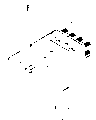
图2显示了本发明的降频器结构;Fig. 2 has shown the downconverter structure of the present invention;

图3a显示了遮挡元件插设于第一探针收纳部时的局部剖面图;Figure 3a shows a partial cross-sectional view of the shielding element when it is inserted into the first probe receiving part;

图3b显示了本发明的降频器所接收到的讯号;Figure 3b shows the signal received by the downconverter of the present invention;

图4显示了本发明的降频器的部分结构;Fig. 4 has shown the partial structure of frequency reducer of the present invention;

图5显示了改良式发夹型滤波器的电路结构。Figure 5 shows the circuit structure of the improved hairpin filter.

具体实施方式 Detailed ways

搭配参照图2和4,本发明的降频器100,其包括一模组框座110、第一探针120、第二探针130、一遮挡元件124、接头140、第一电路板150、第二电路板155、一板材153以及导线。模组框座具有一隔离结构152、第一探针收纳部112以及第二探针收纳部113,设于模组框座110之中,以及一波导管111,设于模组框座110之上。第一探针收纳部112,与波导管111连通,其为一沟槽,具有一圆形开口1121,圆形开口1121的直径大于第一探针收纳部112的沟槽宽度。第一探针120设于第一探针收纳部112之中,并从该波导管111接收第一讯号。遮挡元件124设于第一探针收纳部112之中,以改善探针的讯号接收情形。第二探针130设于第二探针收纳部113之中,并从该波导管111接收第二讯号。第一电路板150与第二电路板155上设有一降频电路,该降频电路将该第一讯号以及该第二讯号分别处理为第一降频讯号以及第二降频讯号。第一电路板150与第二电路板155耦接,以将第一降频讯号以及第二降频讯号从电路板150传递至电路板155,并经由另外导线154穿过隔离结构152,将第二电路板155与板材153耦接,利用第二电路板155与板材153分别将第一降频讯号以及第二降频讯号传递至接头140。2 and 4, the frequency converter 100 of the present invention includes a module frame 110, a first probe 120, a second probe 130, a shielding element 124, a connector 140, a first circuit board 150, The second circuit board 155 , a plate 153 and wires. The module frame has an isolation structure 152, a first probe receiving part 112 and a second probe receiving part 113, which are arranged in the module frame 110, and a waveguide 111, which is arranged in the module frame 110 superior. The first probe receiving portion 112 communicates with the waveguide 111 , and is a groove with a circular opening 1121 . The diameter of the circular opening 1121 is larger than the groove width of the first probe receiving portion 112 . The first probe 120 is disposed in the first probe receiving portion 112 and receives the first signal from the waveguide 111 . The shielding element 124 is disposed in the first probe receiving portion 112 to improve the signal reception of the probe. The second probe 130 is disposed in the second probe receiving portion 113 and receives the second signal from the waveguide 111 . A frequency reduction circuit is disposed on the first circuit board 150 and the second circuit board 155 , and the frequency reduction circuit processes the first signal and the second signal into a first frequency reduction signal and a second frequency reduction signal respectively. The first circuit board 150 is coupled to the second circuit board 155, so as to transmit the first down-frequency signal and the second down-frequency signal from the circuit board 150 to the circuit board 155, and pass through the isolation structure 152 through another wire 154 to transmit the first down-frequency signal and the second down-frequency signal to the circuit board 155. The second circuit board 155 is coupled to the plate 153 , and the first down-frequency signal and the second down-frequency signal are respectively transmitted to the joint 140 by the second circuit board 155 and the plate 153 .

参照图3a,其显示了遮挡元件124与第一探针120插设于第一探针收纳部112之中的情形。第一探针收纳部112为一沟槽。第一探针120具有第一探针导线121以及第一探针隔绝材料122。第一探针导线121由第一导线部分1211以及第二导线部分1212所组成,第一导线部分1211垂直第二导线部分1212。第一探针隔绝材料122包覆于第一导线部分1211。第一探针隔绝材料122呈圆桶状,抵接部123形成于第一探针隔绝材料122之一端,并与第一探针收纳部112的边缘抵接(未图式)。当第一探针120插设于第一探针收纳部112之中时,第一导线部分1211位于圆形开口1121(参照第2图)的位置,该第一探针隔绝材料122以及该第二导线部分1212均埋设于第一探针收纳部112之中,且第二导线部分1212平行于该第一探针收纳部112的底部。遮挡元件124设于第一探针收纳部112中之相对于圆形开1121的另一端。Referring to FIG. 3 a , it shows a situation where the shielding element 124 and the first probe 120 are inserted into the first probe receiving portion 112 . The first probe receiving portion 112 is a groove. The first probe 120 has a first probe wire 121 and a first probe insulating material 122 . The first probe wire 121 is composed of a first wire portion 1211 and a second wire portion 1212 , and the first wire portion 1211 is perpendicular to the second wire portion 1212 . The first probe isolation material 122 covers the first wire portion 1211 . The first probe insulating material 122 is in the shape of a barrel, and the abutting portion 123 is formed at one end of the first probe insulating material 122 and abuts against the edge of the first probe receiving portion 112 (not shown). When the first probe 120 is inserted into the first probe receiving part 112, the first lead part 1211 is located at the position of the circular opening 1121 (refer to FIG. 2 ), the first probe insulating material 122 and the first probe The two wire portions 1212 are buried in the first probe receiving portion 112 , and the second wire portion 1212 is parallel to the bottom of the first probe receiving portion 112 . The shielding element 124 is disposed at the other end of the first probe receiving portion 112 opposite to the circular opening 1121 .

上述的第一探针收纳部112可以为其他形状的凹槽,而遮挡元件124可以为一固定件(如螺丝)或其他可改变第一探针收纳部112共振情形的元件。参照图3b,其显示了设置遮挡元件124后的讯号图,讯号在频率范围12.6~12.7GHz区间(卫星讯号频带)的凹陷已被有效的消除。The above-mentioned first probe receiving portion 112 can be a groove of other shapes, and the shielding element 124 can be a fixing member (such as a screw) or other elements capable of changing the resonance of the first probe receiving portion 112 . Referring to FIG. 3 b , it shows the signal diagram after setting the blocking element 124 , and the notch of the signal in the frequency range of 12.6-12.7 GHz (satellite signal frequency band) has been effectively eliminated.

参照图4,隔离结构152为一长方体,其上形成有贯穿孔1521。导线154穿过贯穿孔1521,并与第二电路板155耦接,而第二电路板155利用导线(未图示)与第一电路板150耦接。导线154表面包覆有导线隔绝材料。导线154的另一端与板材153耦接,接头140与板材153耦接。由于导线154表面包覆有导线隔绝材料,并经过隔离结构152,因此,本发明的降频器100的电压驻波比可以被降至2以下。上述的隔离结构152的材质可以为金属。Referring to FIG. 4 , the isolation structure 152 is a cuboid with through holes 1521 formed thereon. The wire 154 passes through the through hole 1521 and is coupled to the second circuit board 155 , and the second circuit board 155 is coupled to the first circuit board 150 by a wire (not shown). The surface of the wire 154 is coated with a wire insulating material. The other end of the wire 154 is coupled to the plate 153 , and the joint 140 is coupled to the plate 153 . Since the surface of the wire 154 is coated with wire insulating material and passes through the isolation structure 152 , the VSWR of the frequency reducer 100 of the present invention can be reduced to below 2. The above-mentioned isolation structure 152 may be made of metal.

再参照图1d,本发明的降频电路由高频讯号电路2100以及中频讯号电路2200所组成。高频讯号电路包括放大器210、滤波器220、滤波器221、滤波器222、本地震荡器230以及混频器240。高频讯号电路2100将该第一讯号以及该第二讯号分别处理为第一降频讯号以及第二降频讯号。中频讯号电路2200包括放大器250、分配器261、分配器262、切换电路270以及放大器280。中频讯号电路2200将第一降频讯号以及第二降频讯号分流,以提供多输出。高频讯号电路2100设于第一电路板150之上,中频讯号电路2200设于第二电路板155之上。第一电路板150的材料使用Rogers材料或是铁氟龙,第二电路板155的材料使用环氧树脂。如此可由于减少Rogers材料或是铁氟龙等昂贵材料的使用,而可降低成本。此外,第二电路板155可以为四层板,中频讯号电路2200以双面打件的方式设于第二电路板之上,可减少板材面积以及连接次数,以降低成本并便于组装。Referring to FIG. 1d again, the down-frequency circuit of the present invention is composed of a high-frequency signal circuit 2100 and an intermediate-frequency signal circuit 2200 . The high frequency signal circuit includes an amplifier 210 , a filter 220 , a filter 221 , a filter 222 , a local oscillator 230 and a mixer 240 . The high-frequency signal circuit 2100 processes the first signal and the second signal into a first down-frequency signal and a second down-frequency signal, respectively. The intermediate frequency signal circuit 2200 includes an amplifier 250 , a divider 261 , a divider 262 , a switching circuit 270 and an amplifier 280 . The intermediate frequency signal circuit 2200 splits the first down-frequency signal and the second down-frequency signal to provide multiple outputs. The high frequency signal circuit 2100 is disposed on the first circuit board 150 , and the intermediate frequency signal circuit 2200 is disposed on the second circuit board 155 . The material of the first circuit board 150 is Rogers material or Teflon, and the material of the second circuit board 155 is epoxy resin. This can reduce costs by reducing the use of expensive materials such as Rogers material or Teflon. In addition, the second circuit board 155 can be a four-layer board, and the intermediate frequency signal circuit 2200 is provided on the second circuit board by double-sided printing, which can reduce the area of the board and the number of connections, thereby reducing costs and facilitating assembly.

上述的第一讯号以及第二讯号可以为射频讯号,其频率范围为10GHz至13GHz。而第一降频讯号以及第二降频讯号的频率范围为900MHz至2500MHz。The above-mentioned first signal and second signal can be radio frequency signals, and the frequency range is from 10 GHz to 13 GHz. The frequency range of the first down-frequency signal and the second down-frequency signal is 900MHz to 2500MHz.

滤波器221可有效消除该本地震荡器230的二倍频讯号。滤波器221可以为交指型滤波器(interdigital filter,为一种周期为基频周期的三倍的滤波器)或改良式发夹型滤波器(modify hairpin filter)。改良式发夹型滤波器的电路结构如图5所示。改良式发夹型滤波器的相关技术内容,可参考IEEE中的″Hairpinfilters with tunable transmission zeros″论文。The filter 221 can effectively eliminate the double frequency signal of the local oscillator 230 . The filter 221 may be an interdigital filter (a filter whose period is three times that of the fundamental frequency period) or a modified hairpin filter (modify hairpin filter). The circuit structure of the improved hairpin filter is shown in Figure 5. For the relevant technical content of the improved hairpin filter, please refer to the "Hairpinfilters with tunable transmission zeros" paper in IEEE.

本发明利用遮挡元件以改善探针收纳部的共振情形,从而改善降频器的卫星讯号接收情形。此外,隔离结构可将导电产生的电磁波隔离,从而将电压驻波比降低至2以下。本发明并将射频讯号电路以及中频讯号电路分离,并分别设于不同材质的第一电路板以及第二电路板之上,以降低材料成本。The present invention uses the shielding element to improve the resonance of the probe receiving part, so as to improve the satellite signal reception of the down-converter. In addition, the isolation structure can isolate the electromagnetic waves generated by conduction, thereby reducing the voltage standing wave ratio to below 2. In the present invention, the radio frequency signal circuit and the intermediate frequency signal circuit are separated and respectively arranged on the first circuit board and the second circuit board of different materials to reduce material cost.

虽然本发明已参照当前的具体实施例来描述,但是本技术领域中的普通技术人员应当认识到,以上的实施例仅是用来说明本发明,在没有脱离本发明精神的情况下还可作出各种等效的变化或替换,因此,只要在本发明的实质精神范围内对上述实施例的变化、变型都将落在本申请的权利要求书的范围内。Although the present invention has been described with reference to the current specific embodiments, those of ordinary skill in the art should recognize that the above embodiments are only used to illustrate the present invention, and other modifications can be made without departing from the spirit of the present invention. Various equivalent changes or substitutions, therefore, as long as the changes and modifications to the above embodiments are within the spirit of the present invention, they will all fall within the scope of the claims of the present application.

Claims (37)

1. frequency demultiplier comprises:
One module skeleton frame has a waveguide and the first probe incorporating section, and this waveguide is located on this module skeleton frame, and this first probe incorporating section is formed among this module skeleton frame, and is communicated with this waveguide;
First probe is located among this first probe incorporating section, and receives first signal from this waveguide;
One shield element is located among this first probe incorporating section, receives situation with the signal that improves this probe; And
One frequency down circuit is located among this module skeleton frame, and couples with this first probe, and this frequency down circuit is carried out frequency reducing to this first signal.
2. frequency demultiplier as claimed in claim 1 is characterized in that, this first probe is L shaped.
3. frequency demultiplier as claimed in claim 1, it is characterized in that, this first probe has first conductor part, second conductor part and the first probe barrier material, vertical this second conductor part of this first conductor part, this first probe barrier material is coated on this first conductor part, when this first probe was positioned at this first probe incorporating section, this second conductor part was parallel to the bottom of this first probe incorporating section.
4. frequency demultiplier as claimed in claim 1 is characterized in that, this first probe incorporating section is a groove.
5. frequency demultiplier as claimed in claim 1 is characterized in that, this first probe incorporating section is a groove.
6. frequency demultiplier as claimed in claim 5 is characterized in that, an end of this groove has a circular open, and the diameter of this circular open is greater than the width of this groove.
7. frequency demultiplier as claimed in claim 1 is characterized in that, this shield element is a fixture, and this fixture is inserted among this first probe incorporating section.
8. frequency demultiplier as claimed in claim 1 is characterized in that, this shield element is a screw, and this screw is inserted among this first probe incorporating section in the mode that locks.
9. frequency demultiplier comprises:
One module skeleton frame has an isolation structure and a waveguide, and this waveguide is located on this module skeleton frame, and this isolation structure is located among this module skeleton frame, and this isolation structure has a through hole;
One joint is located on this module skeleton frame;
One frequency down circuit is located among this module skeleton frame, and this frequency down circuit receives first signal from this waveguide, and with this first signal frequency reducing, to produce the first frequency reducing signal; And
One lead, this lead passes this isolation structure via this through hole, and couples this frequency down circuit and this joint, and this first frequency reducing signal is passed to this lead from this frequency down circuit, and from this joint output.
10. frequency demultiplier as claimed in claim 9 is characterized in that, this isolation structure is a rectangular structure.
11. frequency demultiplier as claimed in claim 9 is characterized in that, the material of this isolation structure is a metal.
12. frequency demultiplier as claimed in claim 9 is characterized in that, this lead has a lead barrier material, and part is coated on this lead.
13. frequency demultiplier as claimed in claim 9 is characterized in that, more comprises a sheet material, is located on this isolation structure, this first frequency reducing signal through this sheet material, is passed to this joint from this lead.
14. a frequency demultiplier in order to first signal is carried out frequency reducing, comprising:
First circuit board;
Second circuit board, the material of this second circuit board differs from the material of this first circuit board;
One high-frequency signals circuit is located on this first circuit board, and this high-frequency signals circuit is with this first signal frequency reducing, to produce the first frequency reducing signal; And
One intermediate frequency signal circuit is located on this second circuit board, and this intermediate frequency signal circuit and this high-frequency signals circuit couple, and transmits this first frequency reducing signal.
15. frequency demultiplier as claimed in claim 14 is characterized in that, this first circuit board is made by Teflon.
16. frequency demultiplier as claimed in claim 14 is characterized in that, this first circuit board is made by Rogers.
17. frequency demultiplier as claimed in claim 14 is characterized in that, this second circuit board is four laminates.
18. frequency demultiplier as claimed in claim 14 is characterized in that, this first signal is a radio-frequency (RF) signal.
19. frequency demultiplier as claimed in claim 18 is characterized in that, the frequency range of this first signal is 10GHz to 13GHz.
20. frequency demultiplier as claimed in claim 14 is characterized in that, the frequency range of this first frequency reducing signal is 900MHz to 2500MHz.
21. frequency demultiplier as claimed in claim 14 is characterized in that, this second circuit board is made by epoxy resin.
22. a frequency demultiplier comprises:
One module skeleton frame, have a waveguide, the first probe incorporating section and an isolation structure, this waveguide is located on this module skeleton frame, this first probe incorporating section is formed among this module skeleton frame, and be communicated with this waveguide, this isolation structure is located among this module skeleton frame, and this isolation structure has a through hole;
First probe is located among this first probe incorporating section, and receives first signal from this waveguide;
One shield element is located among this first probe incorporating section, receives situation with the signal that improves this probe;
One joint is located on this module skeleton frame;
One frequency down circuit is located among this module skeleton frame, and couples with this first probe, and this frequency down circuit is carried out frequency reducing to this first signal, to produce the first frequency reducing signal; And
One lead, this lead passes this isolation structure via this through hole, and couples this frequency down circuit and this joint, and this first frequency reducing signal is passed to this lead from this frequency down circuit, and from this joint output.
23. frequency demultiplier as claimed in claim 22 is characterized in that, this frequency down circuit comprises first circuit board; Second circuit board, the material of this second circuit board differs from the material of this first circuit board; One high-frequency signals circuit is located on this first circuit board, and this high-frequency signals circuit is with this first signal frequency reducing, to produce this first frequency reducing signal; And an intermediate frequency signal circuit, to be located on this second circuit board, this intermediate frequency signal circuit and this high-frequency signals circuit couple, and transmit this first frequency reducing signal.
24. frequency demultiplier as claimed in claim 23 is characterized in that, this first circuit board is made by Teflon.
25. frequency demultiplier as claimed in claim 23 is characterized in that, this first circuit board is made by Rogers.
26. frequency demultiplier as claimed in claim 23 is characterized in that, this second circuit board is made by epoxy resin.
27. frequency demultiplier as claimed in claim 23 is characterized in that, this second circuit board is four laminates.
28. frequency demultiplier as claimed in claim 23 is characterized in that, this first signal is a radio-frequency (RF) signal.
29. frequency demultiplier as claimed in claim 28 is characterized in that, the frequency range of this first signal is 10GHz to 13GHz.
30. frequency demultiplier as claimed in claim 23 is characterized in that, the frequency range of the first frequency reducing signal is 900MHz to 2500MHz.
31. frequency demultiplier as claimed in claim 22 is characterized in that, this first probe is L shaped.
32. frequency demultiplier as claimed in claim 22 is characterized in that, this first probe incorporating section is a groove.
33. frequency demultiplier as claimed in claim 22 is characterized in that, this shield element is a fixture, and this fixture is inserted among this first probe incorporating section.
34. frequency demultiplier as claimed in claim 22 is characterized in that, this shield element is a screw, and this screw is inserted among this first probe incorporating section in the mode that locks.
35. frequency demultiplier as claimed in claim 22 is characterized in that, this isolation structure is a rectangular structure.
36. frequency demultiplier as claimed in claim 22 is characterized in that, the material of this isolation structure is a metal.
37. frequency demultiplier as claimed in claim 22 is characterized in that, also comprises a sheet material, is located on this isolation structure, this first frequency reducing signal through this sheet material, is passed to this joint from this lead.
CNB2004100324609A 2004-04-09 2004-04-09 Downconverter Expired - Lifetime CN100384103C (en)

Priority Applications (1)

Application Number Priority Date Filing Date Title
CNB2004100324609A CN100384103C (en) 2004-04-09 2004-04-09 Downconverter

Applications Claiming Priority (1)

Application Number Priority Date Filing Date Title
CNB2004100324609A CN100384103C (en) 2004-04-09 2004-04-09 Downconverter

Publications (2)

Publication Number Publication Date
CN1681225A CN1681225A (en) 2005-10-12
CN100384103C true CN100384103C (en) 2008-04-23

Family

ID=35067672

Family Applications (1)

Application Number Title Priority Date Filing Date
CNB2004100324609A Expired - Lifetime CN100384103C (en) 2004-04-09 2004-04-09 Downconverter

Country Status (1)

Country Link
CN (1) CN100384103C (en)

Families Citing this family (1)

* Cited by examiner, † Cited by third party
Publication number Priority date Publication date Assignee Title
TW201944650A (en) * 2018-04-19 2019-11-16 台揚科技股份有限公司 Low noise block down-converter with integrated feed, housing structure thereof, and assembling method thereof

Citations (6)

* Cited by examiner, † Cited by third party
Publication number Priority date Publication date Assignee Title
US3980974A (en) * 1974-04-01 1976-09-14 Tokyo Shibaura Electric Co., Ltd. Compact, waveguide-type microwave transmit-receive apparatus
US4716382A (en) * 1985-11-25 1987-12-29 Yokowo Mfg. Co., Ltd. Microwave amplifying apparatus
CN2057534U (en) * 1989-10-31 1990-05-23 国营国光电子管总厂 Largy power sampling load of adjustable standing-wave ratio waveguide
CN2119058U (en) * 1992-01-22 1992-10-14 中国人民解放军第七三二一工厂 C-band dual-polarized feed source
CN2165534Y (en) * 1993-06-12 1994-05-18 台扬科技股份有限公司 Dual polarising frequency down converter for satellite pick-up antenna
CN2464022Y (en) * 2001-02-27 2001-12-05 兆赫电子股份有限公司 Bipolar Octal Output Multi-Select Satellite Downconverter

Patent Citations (6)

* Cited by examiner, † Cited by third party
Publication number Priority date Publication date Assignee Title
US3980974A (en) * 1974-04-01 1976-09-14 Tokyo Shibaura Electric Co., Ltd. Compact, waveguide-type microwave transmit-receive apparatus
US4716382A (en) * 1985-11-25 1987-12-29 Yokowo Mfg. Co., Ltd. Microwave amplifying apparatus
CN2057534U (en) * 1989-10-31 1990-05-23 国营国光电子管总厂 Largy power sampling load of adjustable standing-wave ratio waveguide
CN2119058U (en) * 1992-01-22 1992-10-14 中国人民解放军第七三二一工厂 C-band dual-polarized feed source
CN2165534Y (en) * 1993-06-12 1994-05-18 台扬科技股份有限公司 Dual polarising frequency down converter for satellite pick-up antenna
CN2464022Y (en) * 2001-02-27 2001-12-05 兆赫电子股份有限公司 Bipolar Octal Output Multi-Select Satellite Downconverter

Non-Patent Citations (1)

* Cited by examiner, † Cited by third party
Title
Hairpin Filters with Tunable Transmission Zeros. Chih-Ming Tsai,Sheng-Yuan Lee,Chin-Chuan Tsai.IEEE MTT-S Digest,Vol.3 . 2001 *

Also Published As

Publication number Publication date
CN1681225A (en) 2005-10-12

Similar Documents

Publication Publication Date Title
US11417938B2 (en) Printed circuit board with substrate-integrated waveguide transition
US10790589B2 (en) Microwave device
CN1087755A (en) Waveguide-Microstrip Switch
JP3769494B2 (en) Polarization separation structure, radio wave receiving converter and antenna device
JP2010272959A (en) High frequency circuit, low noise down converter and antenna device
US20040263280A1 (en) Microstrip-waveguide transition
CN100384103C (en) Downconverter
JP6351450B2 (en) Wireless module, electronic module, and measuring method
US8818319B2 (en) Signal distribution and filtering in low noise block downconverters
US6359593B1 (en) Non-radiating single slotline coupler
US20010043128A1 (en) Broadband flexible printed circuit balun
US7352992B2 (en) Low noise block down converter with integrated feedhorn
JP2001168632A (en) Horn antenna and primary radiator
KR970004856B1 (en) Low noise frequency converter (LNB) with improved polarization characteristics
US20110169710A1 (en) Cross-polarized antenna
CN100511830C (en) Substrate integrated waveguide subharmonic upper frequency changer
JP2001196839A (en) Microwave antenna
US7199755B2 (en) Compact antenna block for a wireless device
JPH04113703A (en) Microwave circuit
KR100822257B1 (en) Radar receiver with triple resonant local oscillation stage
US8378896B2 (en) Wide band antenna
JP2001102802A (en) Converter for satellite broadcasting reception
JP5021351B2 (en) Converter for satellite reception
JP2006136016A (en) Polarization separation structure, radio wave receiving converter and antenna device
JP2005286435A (en) High frequency line-waveguide converter

Legal Events

Date Code Title Description
C06 Publication
PB01 Publication
C10 Entry into substantive examination
SE01 Entry into force of request for substantive examination
C14 Grant of patent or utility model
GR01 Patent grant
CX01 Expiry of patent term

Granted publication date: 20080423