CN100388373C - Super-resolution digital disc with super-lens film structure - Google Patents
Super-resolution digital disc with super-lens film structure Download PDFInfo
- Publication number
- CN100388373C CN100388373C CNB2006100182819A CN200610018281A CN100388373C CN 100388373 C CN100388373 C CN 100388373C CN B2006100182819 A CNB2006100182819 A CN B2006100182819A CN 200610018281 A CN200610018281 A CN 200610018281A CN 100388373 C CN100388373 C CN 100388373C
- Authority
- CN
- China
- Prior art keywords
- super
- dielectric layer
- film
- lens film
- optical disc
- Prior art date
- Legal status (The legal status is an assumption and is not a legal conclusion. Google has not performed a legal analysis and makes no representation as to the accuracy of the status listed.)
- Expired - Fee Related
Links
- 230000003287 optical effect Effects 0.000 claims abstract description 38
- 239000000956 alloy Substances 0.000 claims abstract description 7
- 229910045601 alloy Inorganic materials 0.000 claims abstract description 7
- 229910052581 Si3N4 Inorganic materials 0.000 claims abstract description 6
- HQVNEWCFYHHQES-UHFFFAOYSA-N silicon nitride Chemical compound N12[Si]34N5[Si]62N3[Si]51N64 HQVNEWCFYHHQES-UHFFFAOYSA-N 0.000 claims abstract description 6
- 229910004298 SiO 2 Inorganic materials 0.000 claims description 9
- 239000004417 polycarbonate Substances 0.000 claims description 8
- 239000000463 material Substances 0.000 claims description 7
- 229920000515 polycarbonate Polymers 0.000 claims description 5
- 239000011521 glass Substances 0.000 claims description 4
- 239000012528 membrane Substances 0.000 claims 4
- 239000010410 layer Substances 0.000 abstract description 57
- VYPSYNLAJGMNEJ-UHFFFAOYSA-N silicon dioxide Inorganic materials O=[Si]=O VYPSYNLAJGMNEJ-UHFFFAOYSA-N 0.000 abstract description 7
- 229910052681 coesite Inorganic materials 0.000 abstract description 6
- 229910052906 cristobalite Inorganic materials 0.000 abstract description 6
- 239000000377 silicon dioxide Substances 0.000 abstract description 6
- 229910052682 stishovite Inorganic materials 0.000 abstract description 6
- 229910052905 tridymite Inorganic materials 0.000 abstract description 6
- 235000012239 silicon dioxide Nutrition 0.000 abstract description 4
- 239000002356 single layer Substances 0.000 abstract description 4
- 239000010408 film Substances 0.000 description 38
- 239000010409 thin film Substances 0.000 description 27
- 238000001228 spectrum Methods 0.000 description 10
- 238000010586 diagram Methods 0.000 description 9
- 229910052709 silver Inorganic materials 0.000 description 6
- 230000007423 decrease Effects 0.000 description 5
- 239000000758 substrate Substances 0.000 description 5
- 230000000694 effects Effects 0.000 description 4
- 229910000510 noble metal Inorganic materials 0.000 description 4
- 238000005516 engineering process Methods 0.000 description 3
- 229910052737 gold Inorganic materials 0.000 description 3
- 238000003860 storage Methods 0.000 description 3
- 238000012360 testing method Methods 0.000 description 3
- 238000000034 method Methods 0.000 description 2
- 238000002360 preparation method Methods 0.000 description 2
- 230000001902 propagating effect Effects 0.000 description 2
- 230000009467 reduction Effects 0.000 description 2
- 230000009471 action Effects 0.000 description 1
- 238000013459 approach Methods 0.000 description 1
- 230000008859 change Effects 0.000 description 1
- 238000011161 development Methods 0.000 description 1
- 238000002474 experimental method Methods 0.000 description 1
- 238000001755 magnetron sputter deposition Methods 0.000 description 1
- 238000004519 manufacturing process Methods 0.000 description 1
- 230000007246 mechanism Effects 0.000 description 1
- 239000000203 mixture Substances 0.000 description 1
- 238000003825 pressing Methods 0.000 description 1
- 238000004886 process control Methods 0.000 description 1
- 239000011241 protective layer Substances 0.000 description 1
- 239000004065 semiconductor Substances 0.000 description 1
- 238000004544 sputter deposition Methods 0.000 description 1
Images


Landscapes
- Optical Head (AREA)
- Optical Record Carriers And Manufacture Thereof (AREA)
Abstract
一种超透镜薄膜结构的超分辨数字光盘,包括超透镜薄膜(2)和盘基(3),还有介电层(1),它们依次为介电层(1)/超透镜薄膜(2)/盘基(3),介电层(1)是氮化硅SiN或ZnS-SiO2;盘基(3)带有坑点,坑点尺寸小于380nm,最小坑点尺寸在200nm,其特征在于:超透镜薄膜(2)是Ag(x)Au(1-x)合金薄膜,其中x值在0-1之间变化。该光盘结构,通过使用激光波长为650nm红光,数值孔径为0.60的光学头,实现信息坑点尺寸在200nm及其以上的动态读出。该光盘的单面单层容量达到12-15GB,双面单层的容量达到25-30GB。
A super-resolution digital optical disc with a super-lens film structure, comprising a super-lens film (2) and a disc base (3), and a dielectric layer (1), which are dielectric layer (1)/super-lens film (2)/disc base (3) in sequence, wherein the dielectric layer (1) is silicon nitride SiN or ZnS- SiO2 ; the disc base (3) has pits, the pit size is less than 380nm, and the minimum pit size is 200nm, and the characteristic is that the super-lens film (2) is an Ag(x)Au(1-x) alloy film, wherein the x value varies between 0 and 1. The optical disc structure realizes dynamic reading of information pit size of 200nm or above by using an optical head with a laser wavelength of 650nm red light and a numerical aperture of 0.60. The single-sided single-layer capacity of the optical disc reaches 12-15GB, and the double-sided single-layer capacity reaches 25-30GB.
Description
技术领域 technical field
本发明属于信息技术中光存储领域,是一种超透镜薄膜结构的超分辨数字光盘,主要适用于只读式红光超分辨数字光盘,可以有音频、视频等多种用途。The invention belongs to the field of optical storage in information technology, and is a super-resolution digital disc with a super-lens thin film structure, which is mainly suitable for read-only red light super-resolution digital discs, and can be used for multiple purposes such as audio and video.
背景技术 Background technique
信息技术的迅猛发展要求用于信息存储的光盘必须具备超高存储密度和超快存取速率,这就要求光盘中的记录点的尺寸越来越小。然而,随着记录点尺寸的减小,要求用于记录点读出的光斑尺寸也相应减小,采用现有的光学系统却很难读出如此微小的记录点,因为记录点尺寸小于读出光斑的分辨率,光斑中将出现多个记录点的信号,这就要求采用短波长的激光和高数值孔径的光学头,但由于光的衍射极限效应和光学头的数值孔径的制约,读出光斑尺寸的减小即使从目前的蓝光转移到紫光也只是几倍的关系,而光学头数值孔径的增大是以焦深的减小和由于偏心率而引起的失真的加大为代价。因此采用增大光学头的数值孔径和减小激光波长来减小读出光斑的尺寸是十分有限的,所以研究直径小于光的衍射极限的记录点(超分辨记录点)的读出具有非常重要的应用价值和意义,同时这对于实现超高容量的只读式光盘来讲也有很大的实际应用前景。Yasuda等首次采用“PC基片/介电层/反射层/介电层/掩膜层/介电层”的膜层结构在只读式光盘中实现了超分辨记录点的读出(Kouichi Yasuda,Masumi Ono and Katsuhisa Aratani et al.Premastered OpticalDisk by Super-resolution.Jpn.J.Appl.Phys.,1993,32(11B):5210-5213),随后他们改变光盘结构为“PC基片/对比度增强层/介电层/掩膜层/介电层/反射层/介电层”既实现了只读式超分辨光盘的线密度提高,又实现了其道密度的增加(Yutaka K,Kouichi Y,Masumi O et al.,Jpn.J.Appl.Phys.,1996,35 part.1B 423-428)。Yihong Wu等在理论上提出“PC基片/介电层/上掩膜层/下掩膜层/反射层/介电层”双掩膜层结构的只读式超分辨光盘来获得超分辨记录点的读出(Yihong Wu,Hock Khoo and Takuyo Kogure et al.Read-only Optical disk with Super-resolution,Appl.Phys.Lett.1994,64(24):3225-3227)。Jingsong Wei and Fuxi Gan采用超分辨反射膜结构在激光波长为632.8nm、光学头的数值孔径为0.40的装置上实现了尺寸为380nm的超分辨信息点的读出。(Jingsong Wei and Fuxi Gan,“Novel approach to super-resolution pits readout”,Opt.Eng.(Lett)41(9),2073-2074(2002)。然而,以上的光盘结构读出的记录点尺寸仅仅在光的衍射极限左右,我们的任务是进一步读出更小的记录点和得到更高的信噪比,使光盘上的信息记录点小于380nm。The rapid development of information technology requires that the optical disc used for information storage must have ultra-high storage density and ultra-fast access rate, which requires that the size of the recording point in the optical disc is getting smaller and smaller. However, as the size of the recording point decreases, the spot size required for reading the recording point also decreases accordingly. It is difficult to read such a small recording point with the existing optical system, because the size of the recording point is smaller than the readout The resolution of the spot, the signal of multiple recording points will appear in the spot, which requires the use of short-wavelength laser and high numerical aperture optical head, but due to the diffraction limit effect of light and the restriction of the numerical aperture of the optical head, the readout Even if the reduction of the spot size is transferred from the current blue light to the purple light, it is only a few times, and the increase of the numerical aperture of the optical head is at the expense of the reduction of the focal depth and the increase of the distortion caused by the eccentricity. Therefore, it is very limited to increase the numerical aperture of the optical head and reduce the laser wavelength to reduce the size of the read spot, so it is very important to study the readout of the record point (super-resolution record point) whose diameter is smaller than the diffraction limit of light. The application value and significance, and it also has great practical application prospects for realizing ultra-high capacity read-only optical discs. For the first time, Yasuda et al. used the film layer structure of "PC substrate/dielectric layer/reflective layer/dielectric layer/mask layer/dielectric layer" to realize the readout of super-resolution recording points in a read-only optical disc (Kouichi Yasuda , Masumi Ono and Katsuhisa Aratani et al.Premastered OpticalDisk by Super-resolution.Jpn.J.Appl.Phys., 1993, 32(11B): 5210-5213), then they changed the optical disk structure to "PC substrate/contrast enhancement layer/dielectric layer/mask layer/dielectric layer/reflective layer/dielectric layer" not only improves the line density of read-only super-resolution optical discs, but also increases the track density (Yutaka K, Kouichi Y, Masumi O et al., Jpn. J. Appl. Phys., 1996, 35 part. 1B 423-428). Yihong Wu et al. theoretically proposed a read-only super-resolution optical disc with a double-mask layer structure of "PC substrate/dielectric layer/upper mask layer/lower mask layer/reflective layer/dielectric layer" to obtain super-resolution recording. Point readout (Yihong Wu, Hock Khoo and Takuyo Kogure et al. Read-only Optical disk with Super-resolution, Appl. Phys. Lett. 1994, 64(24): 3225-3227). Jingsong Wei and Fuxi Gan used a super-resolution reflective film structure to realize the readout of super-resolution information points with a size of 380nm on a device with a laser wavelength of 632.8nm and an optical head with a numerical aperture of 0.40. (Jingsong Wei and Fuxi Gan, "Novel approach to super-resolution pits readout", Opt. Eng. (Lett) 41 (9), 2073-2074 (2002). However, the recording point size read out by the above optical disc structure is only Around the diffraction limit of light, our task is to further read out smaller recording points and obtain a higher signal-to-noise ratio, so that the information recording points on the optical disc are smaller than 380nm.
发明内容 Contents of the invention
为了能读出只读式光盘中小于380nm的信息记录点,本发明提出一种超透镜薄膜结构的超分辨数字光盘,在激光波长为650nm、数值孔径为0.60的动态装置上实现记录点尺寸在200nm及其以上的读出,该记录点的尺寸远小于动态测试装置的分辨率。In order to be able to read the information recording points less than 380nm in the read-only optical disc, the present invention proposes a super-resolution digital optical disc with a super-lens film structure, which realizes the recording point size on a dynamic device with a laser wavelength of 650nm and a numerical aperture of 0.60. For readout of 200nm and above, the size of the recording spot is much smaller than the resolution of the dynamic test device.
本发明的技术解决方案是:Technical solution of the present invention is:
一种超透镜薄膜结构的超分辨数字光盘,包括超透镜薄膜2和盘基3,其特征在于:还有介电层1,它们依次为介电层1/超透镜薄膜2/盘基3,介电层1是氮化硅SiN或ZnS-SiO2;超透镜薄膜2是Ag、Au或Ag(x)Au(1-x)合金薄膜,其中x值在0-1之间变化;盘基3带有坑点,坑点尺寸小于380nm,最小坑点尺寸在200nm。由于采用了上述结构,与在先技术相比具有结构简单、制备成本低廉和工艺控制容易等优良性能。其机理是在读出激光束的作用下,由于超透镜薄膜由贵金属组成,其上又覆盖了介电层1,在介电层1/超透镜薄膜2的界面处会激发出表面等离子体波,表面等离子体波由于沿表面传播,波矢大、波长短,当遇到信息记录点时,它将被散射和耦合成传播光,通过探测该传播光来实现更小超分辨记录点的动态读出。A super-resolution digital disc with a super-lens film structure, comprising a
如上所述的超透镜薄膜结构的超分辨数字光盘,其特征在于所述的超透镜薄膜2所用的Ag、Au或Ag(x)Au(1-x)合金薄膜材料的厚度范围5-500nm。在5-500nm区间中,具有读出信噪比高,光盘性能稳定等优良性能。The super-resolution digital disc with the above-mentioned super-lens film structure is characterized in that the Ag, Au or Ag(x)Au(1-x) alloy film material used in the
如上所述的超透镜薄膜结构的超分辨数字光盘,其特征在于介电层1由厚度10-500nm的氮化硅SiN或ZnS-SiO2构成,厚度范围是10--500nm。在10--500nm区间中,具有具有读出信噪比高,光盘性能稳定等优良性能。The above-mentioned super-resolution digital disc with super-lens film structure is characterized in that the
如上所述的超透镜薄膜结构的超分辨数字光盘,其特征在于所述的盘基3所用的材料为聚碳酸酯或K9玻璃,盘基的厚度为0.6-1.2mm。盘基3可用的材料有用聚碳酸酯或K9玻璃或普通的石英玻璃,选用聚碳酸酯或K9玻璃具有读出性能好、材料来源容易、与传统光盘兼容等优良性能。The above-mentioned super-resolution digital disc with super-lens film structure is characterized in that the material used for the
本发明的技术效果:Technical effect of the present invention:
与先前的技术相比,本发明的超透镜薄膜结构的超分辨数字光盘中介电层1为保护层,并与超透镜薄膜层2结合用于减小读出光斑的尺寸。在激光波长为650nm、光学头的数值孔径为0.60的动态测试系统下能实现信息坑点尺寸在200nm及200nm以上的读出。该只读式光盘的单面单层容量达到12-15GB,双面单层的容量达到25-30GB。Compared with the previous technology, the
附图说明 Description of drawings
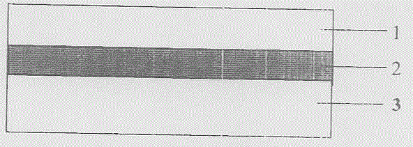
图1,本发明实施例的结构示意图。Fig. 1 is a schematic structural diagram of an embodiment of the present invention.
图2,以SiN作为介电层、Ag作为超透镜薄膜得到的动态信号示波器图。Figure 2, the dynamic signal oscilloscope diagram obtained by using SiN as the dielectric layer and Ag as the metalens film.
图3,以SiN作为介电层、Au作超透镜薄膜得到的动态读出信号频谱图。Figure 3, the dynamic readout signal spectrum obtained by using SiN as the dielectric layer and Au as the metalens film.
图4,以SiN作为介电层,Ag0.5Au0.5超透镜薄膜得到的读出信号频谱图。Fig. 4, using SiN as the dielectric layer, Ag 0.5 Au 0.5 metalens thin film readout signal spectrum.
图5,以ZnS-SiO2作为介电层,Ag作超透镜薄膜得到的读出信号的频谱图。Fig. 5 is the spectrum diagram of the readout signal obtained by using ZnS-SiO 2 as the dielectric layer and Ag as the superlens film.
图6,以ZnS-SiO2作为介电层,Au作超透镜薄膜得到的读出信号的频谱图。Figure 6, the spectrum diagram of the readout signal obtained by using ZnS-SiO 2 as the dielectric layer and Au as the metalens film.
图7,以ZnS-SiO2作为介电层,Ag0.5Au0.5作超透镜薄膜得到的信号的频谱图。Fig. 7, the frequency spectrum of the signal obtained by using ZnS-SiO 2 as the dielectric layer and Ag 0.5 Au 0.5 as the metalens film.
图8,SiN薄膜厚度与读出信噪比的关系。Figure 8, the relationship between SiN film thickness and readout signal-to-noise ratio.
图9,ZnS-SiO2薄膜厚度与读出信噪比的关系。Figure 9. Relationship between ZnS- SiO2 film thickness and readout signal-to-noise ratio.
图10,Ag薄膜厚度与读出信噪比的关系。Figure 10, the relationship between Ag film thickness and readout signal-to-noise ratio.
图11,Au薄膜厚度与读出信噪比的关系。Figure 11, the relationship between Au film thickness and readout signal-to-noise ratio.
图12,Ag0.5Au0.5薄膜厚度与读出信噪比的关系。Figure 12, the relationship between Ag 0.5 Au 0.5 film thickness and readout signal-to-noise ratio.
具体实施方式 Detailed ways
本发明的实施例为″超透镜薄膜结构的只读式红光超分辨多用数字光盘”,如图1所示,包括介电层1、超透镜薄膜层2和盘基3。介电层1用于保护超透镜薄膜层2,并与超透镜薄膜层2结合用于减小读出光斑的尺寸,盘基3用于预制信息点,信息点尺寸在200nm。The embodiment of the present invention is a "read-only red light super-resolution multi-purpose digital disc with a super-lens film structure", as shown in FIG. The
本发明实施例中的介电层1由厚度10-500nm的氮化硅或ZnS-SiO2构成.根据实施的具体情况取值,然而,在低于10nm时,则不行,因为在该厚度下高质量的薄膜制备比较困难;在高于500nm时也不行,因为在该厚度下一方面使制备成本提高,另一方面读出信号下降。超透镜薄膜层2所用的材料的厚度为5-500nm的Ag、Au或Ag(x)Au(1-x)合金薄膜,根据实施的具体情况取值,在低于5nm时则不行,因为在该厚度下高质量的薄膜制备比较困难,同时降低光盘的读出信噪比,高于500nm时也不行,因为在该厚度下已经没有表面等离子体波效应,不能实现超分辨信息点的动态读出。介电层1、超透镜薄膜层2和盘基3联合构成超透镜薄膜结构的超分辨数字光盘,见图1。
本发明的介电层1可以由SiN(x)或ZnS(x)-SiO2(1-x)构成,超透镜薄膜2可以由Ag(x)、Au(1-x)或Ag(x)Au(1-x)合金组成(注:参数x可以取0和1之间的任意值)。下面结合实例对本发明及其作用作进一步说明:The
在厚度为0.6mm的聚碳酸酯基片上用压制的方法预制直径为200nm的坑点作为信息点。超透镜薄膜结构的只读式红光超分辨多用数字光盘的制备过程如下:采用磁控溅射方法(溅射气压1.0×10⁻⁴Pa),在光盘基片上依次镀:贵金属薄膜层2和介电层1,其中介电层1为厚度为80nm的SiN薄膜,贵金属薄膜层2为40nm厚的Ag超透镜薄膜。检测光盘中信号所用装置的激光器是波长为650nm的半导体激光器,所用光学头的数值孔径为0.60,根据光的衍射极限公式计算得到光斑的半高宽的直径为600nm,远远超过坑点直径200nm。测试本实验中的超透镜薄膜结构的只读式红光超分辨多用数字光盘,则得到了图2所示的示波器信号,这说明本发明“超透镜薄膜结构的只读式红光超分辨多用数字光盘”能在激光波长为650nm、光学头的数值孔径为0.60的动态装置上实现信息坑点尺寸在200nm的读出。以SiN作为介电层,Au作为超透镜薄膜层得到的动态读出信号的频谱图3。以SiN作为介电层,Ag0.5Au0.5作为超透镜薄膜层得到的动态读出信号的频谱图4。以ZnS-SiO2作为介电层,Ag作为超透镜薄膜层得到的动态读出信号的频谱图5。以ZnS-SiO2作为介电层,Au作为超透镜薄膜层得到的动态读出信号的频谱图6。以ZnS-SiO2作为介电层,Ag0.5Au0.5作为贵金属薄膜层得到的动态读出信号的频谱图7。On the polycarbonate substrate with a thickness of 0.6mm, pits with a diameter of 200nm are prefabricated as information points by pressing. The preparation process of the read-only red light super-resolution multi-purpose digital disc with the metalens thin film structure is as follows: using the magnetron sputtering method (sputtering pressure 1.0×10 -4 Pa), sequentially plate: noble metal
改变上述SiN薄膜或ZnS-SiO2薄膜厚度得到图8和图9所示的动态读出信号与薄膜厚度的关系,其关系为随着薄膜厚度的增加,其信噪比先增加再减小。SiN薄膜或ZnS-SiO2薄膜厚度在200nm左右时,信噪比达到最大值。Changing the above-mentioned SiN film or ZnS- SiO2 film thickness can obtain the relationship between the dynamic readout signal and the film thickness shown in Figure 8 and Figure 9, and the relationship is that as the film thickness increases, the signal-to-noise ratio first increases and then decreases. When the thickness of SiN film or ZnS-SiO 2 film is about 200nm, the signal-to-noise ratio reaches the maximum value.
改变Ag薄膜或Au薄膜或Ag0.5Au0.5薄膜的厚度,得到图10、图11、图12所示的读出信噪比与薄膜厚度的关系,其关系为随着薄膜厚度的增加,其信噪比先增加再减小。Ag薄膜,Au薄膜,Ag0.5Au0.5薄膜的厚度分别在300nm,220nm,320nm左右时,信噪比达到最大值。Change the thickness of Ag thin film or Au thin film or Ag 0.5 Au 0.5 thin film, obtain the relationship between the read signal-to-noise ratio and the film thickness shown in Fig. The noise ratio first increases and then decreases. When the thickness of Ag thin film, Au thin film, Ag 0.5 Au 0.5 thin film is about 300nm, 220nm, 320nm respectively, the signal-to-noise ratio reaches the maximum value.
综上所述,采用本发明的“超透镜薄膜结构的只读式红光超分辨多用数字光盘”,在激光波长为650nm、光学头的数值孔径为0.60的动态装置上能实现信息坑点尺寸在200nm及其以上的读出。In summary, adopting the "read-only red light super-resolution multi-purpose digital disc with a hyperlens thin film structure" of the present invention, the information pit size can be realized on a dynamic device where the laser wavelength is 650nm and the numerical aperture of the optical head is 0.60. Readout at 200nm and above.
Claims (4)
Priority Applications (1)
| Application Number | Priority Date | Filing Date | Title |
|---|---|---|---|
| CNB2006100182819A CN100388373C (en) | 2006-01-23 | 2006-01-23 | Super-resolution digital disc with super-lens film structure |
Applications Claiming Priority (1)
| Application Number | Priority Date | Filing Date | Title |
|---|---|---|---|
| CNB2006100182819A CN100388373C (en) | 2006-01-23 | 2006-01-23 | Super-resolution digital disc with super-lens film structure |
Publications (2)
| Publication Number | Publication Date |
|---|---|
| CN1822150A CN1822150A (en) | 2006-08-23 |
| CN100388373C true CN100388373C (en) | 2008-05-14 |
Family
ID=36923443
Family Applications (1)
| Application Number | Title | Priority Date | Filing Date |
|---|---|---|---|
| CNB2006100182819A Expired - Fee Related CN100388373C (en) | 2006-01-23 | 2006-01-23 | Super-resolution digital disc with super-lens film structure |
Country Status (1)
| Country | Link |
|---|---|
| CN (1) | CN100388373C (en) |
Families Citing this family (1)
| Publication number | Priority date | Publication date | Assignee | Title |
|---|---|---|---|---|
| GB0614343D0 (en) * | 2006-07-19 | 2006-08-30 | Univ Southampton | Subwavelength focusing without superlens |
Citations (4)
| Publication number | Priority date | Publication date | Assignee | Title |
|---|---|---|---|---|
| CN1220455A (en) * | 1997-11-25 | 1999-06-23 | 三星电子株式会社 | Phase change optical disk having reflection layer of noble metal, and optical data storage system therefor |
| CN1542788A (en) * | 2003-11-07 | 2004-11-03 | 中国科学院上海光学精密机械研究所 | Super-resolution reflective film structure |
| CN1632870A (en) * | 2004-12-21 | 2005-06-29 | 中国科学院上海光学精密机械研究所 | High-density enhanced read-only digital optical disk |
| CN1632869A (en) * | 2004-12-21 | 2005-06-29 | 中国科学院上海光学精密机械研究所 | High-density enhanced recordable multipurpose digital optical disk |
-
2006
- 2006-01-23 CN CNB2006100182819A patent/CN100388373C/en not_active Expired - Fee Related
Patent Citations (4)
| Publication number | Priority date | Publication date | Assignee | Title |
|---|---|---|---|---|
| CN1220455A (en) * | 1997-11-25 | 1999-06-23 | 三星电子株式会社 | Phase change optical disk having reflection layer of noble metal, and optical data storage system therefor |
| CN1542788A (en) * | 2003-11-07 | 2004-11-03 | 中国科学院上海光学精密机械研究所 | Super-resolution reflective film structure |
| CN1632870A (en) * | 2004-12-21 | 2005-06-29 | 中国科学院上海光学精密机械研究所 | High-density enhanced read-only digital optical disk |
| CN1632869A (en) * | 2004-12-21 | 2005-06-29 | 中国科学院上海光学精密机械研究所 | High-density enhanced recordable multipurpose digital optical disk |
Non-Patent Citations (1)
| Title |
|---|
| 一种新的超分辨记录点的读出技术. 魏劲松,阮昊,施宏仁,干福熹.光学学报,第23卷第5期. 2003 * |
Also Published As
| Publication number | Publication date |
|---|---|
| CN1822150A (en) | 2006-08-23 |
Similar Documents
| Publication | Publication Date | Title |
|---|---|---|
| TW527592B (en) | Optical information recording media, and the manufacturing method and record regeneration method of the same | |
| KR20060032155A (en) | Optical recording medium, optical recording / reproducing apparatus, optical recording apparatus and optical reproducing apparatus, data recording / reproducing method and data recording method and data reproducing method for optical recording medium | |
| KR0168626B1 (en) | Thermomagnetic recording of information and optical reading method of information, and a recording element and a method of manufacturing the recording element suitable for use therein | |
| US8101258B2 (en) | High density information storage medium having plasmonic nano device | |
| TW200400495A (en) | Optical recording reproduction method and optical recording medium | |
| CN101541554B (en) | Optical recording medium and method for manufacturing the same | |
| CN100388373C (en) | Super-resolution digital disc with super-lens film structure | |
| CN100385538C (en) | Dual stack optical data storage medium | |
| CN111508533B (en) | Nano photoetching-based optical disk and physical storage medium structure and writing and reading method thereof | |
| JP2002312978A (en) | Phase change optical disk | |
| JPH11283278A (en) | Optical recording medium | |
| CN1155948C (en) | Method for recording, erasing and reading imformation of near-field dual-photon storage | |
| CN1632870A (en) | High-density enhanced read-only digital optical disk | |
| WO2007088682A1 (en) | Information recording medium, method for producing same, and apparatus for producing same | |
| CN101271707A (en) | Optical recording medium and manufacturing method thereof | |
| CN1199168C (en) | Optical disk | |
| TWI225245B (en) | Method of reproducing optical recording medium with high recording density | |
| CN100580783C (en) | Write-once type optical recording medium | |
| CN1632869A (en) | High-density enhanced recordable multipurpose digital optical disk | |
| CN101981620A (en) | Information recording medium, recording device, reproduction device, and reproduction method | |
| JPS6040542A (en) | optical memory medium | |
| CN1542788A (en) | Super-resolution reflective film structure | |
| JPH06267113A (en) | Optical disk exclusively used for reproduction | |
| JP2008165952A (en) | Optical recording medium | |
| JPH038148A (en) | Magneto-optical recording medium |
Legal Events
| Date | Code | Title | Description |
|---|---|---|---|
| C06 | Publication | ||
| PB01 | Publication | ||
| C10 | Entry into substantive examination | ||
| SE01 | Entry into force of request for substantive examination | ||
| C14 | Grant of patent or utility model | ||
| GR01 | Patent grant | ||
| ASS | Succession or assignment of patent right |
Owner name: SHANGHAI OPTICS AND PRECISION MECHANICS INSTITUTE Free format text: FORMER OWNER: SHANGHAI OPTICS AND PRECISION MECHANICS INSTITUTE, CHINESE ACADEMY OF SCIENCES; ZHA LI Effective date: 20080905 |
|
| C41 | Transfer of patent application or patent right or utility model | ||
| TR01 | Transfer of patent right |
Effective date of registration: 20080905 Address after: Shanghai 800-211 post office mailbox: 201800 Co-patentee after: Wuhan Guanggu Gaoqing Technology Development Co., Ltd. Patentee after: Shanghai Institute of Optics and Fine Mechanics.CAS, Chinese Academy of Sciences Address before: Shanghai 800-211 post office mailbox: 201800 Co-patentee before: Cha Li Patentee before: Shanghai Institute of Optics and Fine Mechanics.CAS, Chinese Academy of Sciences |
|
| CF01 | Termination of patent right due to non-payment of annual fee |
Granted publication date: 20080514 Termination date: 20170123 |
|
| CF01 | Termination of patent right due to non-payment of annual fee |