CN100399511C - Compound semiconductor substrate and manufacturing method thereof - Google Patents
Compound semiconductor substrate and manufacturing method thereof Download PDFInfo
- Publication number
- CN100399511C CN100399511C CNB2005100842833A CN200510084283A CN100399511C CN 100399511 C CN100399511 C CN 100399511C CN B2005100842833 A CNB2005100842833 A CN B2005100842833A CN 200510084283 A CN200510084283 A CN 200510084283A CN 100399511 C CN100399511 C CN 100399511C
- Authority
- CN
- China
- Prior art keywords
- layer
- support
- seed layer
- working
- working layer
- Prior art date
- Legal status (The legal status is an assumption and is not a legal conclusion. Google has not performed a legal analysis and makes no representation as to the accuracy of the status listed.)
- Expired - Lifetime
Links
Images


Classifications
-
- H—ELECTRICITY
- H10—SEMICONDUCTOR DEVICES; ELECTRIC SOLID-STATE DEVICES NOT OTHERWISE PROVIDED FOR
- H10P—GENERIC PROCESSES OR APPARATUS FOR THE MANUFACTURE OR TREATMENT OF DEVICES COVERED BY CLASS H10
- H10P10/00—Bonding of wafers, substrates or parts of devices
-
- C—CHEMISTRY; METALLURGY
- C30—CRYSTAL GROWTH
- C30B—SINGLE-CRYSTAL GROWTH; UNIDIRECTIONAL SOLIDIFICATION OF EUTECTIC MATERIAL OR UNIDIRECTIONAL DEMIXING OF EUTECTOID MATERIAL; REFINING BY ZONE-MELTING OF MATERIAL; PRODUCTION OF A HOMOGENEOUS POLYCRYSTALLINE MATERIAL WITH DEFINED STRUCTURE; SINGLE CRYSTALS OR HOMOGENEOUS POLYCRYSTALLINE MATERIAL WITH DEFINED STRUCTURE; AFTER-TREATMENT OF SINGLE CRYSTALS OR A HOMOGENEOUS POLYCRYSTALLINE MATERIAL WITH DEFINED STRUCTURE; APPARATUS THEREFOR
- C30B25/00—Single-crystal growth by chemical reaction of reactive gases, e.g. chemical vapour-deposition growth
- C30B25/02—Epitaxial-layer growth
-
- C—CHEMISTRY; METALLURGY
- C30—CRYSTAL GROWTH
- C30B—SINGLE-CRYSTAL GROWTH; UNIDIRECTIONAL SOLIDIFICATION OF EUTECTIC MATERIAL OR UNIDIRECTIONAL DEMIXING OF EUTECTOID MATERIAL; REFINING BY ZONE-MELTING OF MATERIAL; PRODUCTION OF A HOMOGENEOUS POLYCRYSTALLINE MATERIAL WITH DEFINED STRUCTURE; SINGLE CRYSTALS OR HOMOGENEOUS POLYCRYSTALLINE MATERIAL WITH DEFINED STRUCTURE; AFTER-TREATMENT OF SINGLE CRYSTALS OR A HOMOGENEOUS POLYCRYSTALLINE MATERIAL WITH DEFINED STRUCTURE; APPARATUS THEREFOR
- C30B25/00—Single-crystal growth by chemical reaction of reactive gases, e.g. chemical vapour-deposition growth
- C30B25/02—Epitaxial-layer growth
- C30B25/18—Epitaxial-layer growth characterised by the substrate
-
- C—CHEMISTRY; METALLURGY
- C30—CRYSTAL GROWTH
- C30B—SINGLE-CRYSTAL GROWTH; UNIDIRECTIONAL SOLIDIFICATION OF EUTECTIC MATERIAL OR UNIDIRECTIONAL DEMIXING OF EUTECTOID MATERIAL; REFINING BY ZONE-MELTING OF MATERIAL; PRODUCTION OF A HOMOGENEOUS POLYCRYSTALLINE MATERIAL WITH DEFINED STRUCTURE; SINGLE CRYSTALS OR HOMOGENEOUS POLYCRYSTALLINE MATERIAL WITH DEFINED STRUCTURE; AFTER-TREATMENT OF SINGLE CRYSTALS OR A HOMOGENEOUS POLYCRYSTALLINE MATERIAL WITH DEFINED STRUCTURE; APPARATUS THEREFOR
- C30B29/00—Single crystals or homogeneous polycrystalline material with defined structure characterised by the material or by their shape
- C30B29/10—Inorganic compounds or compositions
- C30B29/40—AIIIBV compounds wherein A is B, Al, Ga, In or Tl and B is N, P, As, Sb or Bi
- C30B29/403—AIII-nitrides
-
- C—CHEMISTRY; METALLURGY
- C30—CRYSTAL GROWTH
- C30B—SINGLE-CRYSTAL GROWTH; UNIDIRECTIONAL SOLIDIFICATION OF EUTECTIC MATERIAL OR UNIDIRECTIONAL DEMIXING OF EUTECTOID MATERIAL; REFINING BY ZONE-MELTING OF MATERIAL; PRODUCTION OF A HOMOGENEOUS POLYCRYSTALLINE MATERIAL WITH DEFINED STRUCTURE; SINGLE CRYSTALS OR HOMOGENEOUS POLYCRYSTALLINE MATERIAL WITH DEFINED STRUCTURE; AFTER-TREATMENT OF SINGLE CRYSTALS OR A HOMOGENEOUS POLYCRYSTALLINE MATERIAL WITH DEFINED STRUCTURE; APPARATUS THEREFOR
- C30B29/00—Single crystals or homogeneous polycrystalline material with defined structure characterised by the material or by their shape
- C30B29/10—Inorganic compounds or compositions
- C30B29/40—AIIIBV compounds wherein A is B, Al, Ga, In or Tl and B is N, P, As, Sb or Bi
- C30B29/403—AIII-nitrides
- C30B29/406—Gallium nitride
-
- H—ELECTRICITY
- H10—SEMICONDUCTOR DEVICES; ELECTRIC SOLID-STATE DEVICES NOT OTHERWISE PROVIDED FOR
- H10D—INORGANIC ELECTRIC SEMICONDUCTOR DEVICES
- H10D62/00—Semiconductor bodies, or regions thereof, of devices having potential barriers
- H10D62/80—Semiconductor bodies, or regions thereof, of devices having potential barriers characterised by the materials
- H10D62/83—Semiconductor bodies, or regions thereof, of devices having potential barriers characterised by the materials being Group IV materials, e.g. B-doped Si or undoped Ge
- H10D62/832—Semiconductor bodies, or regions thereof, of devices having potential barriers characterised by the materials being Group IV materials, e.g. B-doped Si or undoped Ge being Group IV materials comprising two or more elements, e.g. SiGe
- H10D62/8325—Silicon carbide
-
- H—ELECTRICITY
- H10—SEMICONDUCTOR DEVICES; ELECTRIC SOLID-STATE DEVICES NOT OTHERWISE PROVIDED FOR
- H10P—GENERIC PROCESSES OR APPARATUS FOR THE MANUFACTURE OR TREATMENT OF DEVICES COVERED BY CLASS H10
- H10P90/00—Preparation of wafers not covered by a single main group of this subclass, e.g. wafer reinforcement
- H10P90/19—Preparing inhomogeneous wafers
- H10P90/1904—Preparing vertically inhomogeneous wafers
-
- H—ELECTRICITY
- H10—SEMICONDUCTOR DEVICES; ELECTRIC SOLID-STATE DEVICES NOT OTHERWISE PROVIDED FOR
- H10P—GENERIC PROCESSES OR APPARATUS FOR THE MANUFACTURE OR TREATMENT OF DEVICES COVERED BY CLASS H10
- H10P90/00—Preparation of wafers not covered by a single main group of this subclass, e.g. wafer reinforcement
- H10P90/19—Preparing inhomogeneous wafers
- H10P90/1904—Preparing vertically inhomogeneous wafers
- H10P90/1906—Preparing SOI wafers
- H10P90/1914—Preparing SOI wafers using bonding
- H10P90/1916—Preparing SOI wafers using bonding with separation or delamination along an ion implanted layer, e.g. Smart-cut
-
- H—ELECTRICITY
- H10—SEMICONDUCTOR DEVICES; ELECTRIC SOLID-STATE DEVICES NOT OTHERWISE PROVIDED FOR
- H10P—GENERIC PROCESSES OR APPARATUS FOR THE MANUFACTURE OR TREATMENT OF DEVICES COVERED BY CLASS H10
- H10P90/00—Preparation of wafers not covered by a single main group of this subclass, e.g. wafer reinforcement
- H10P90/22—Preparation of wafers not covered by a single main group of this subclass, e.g. wafer reinforcement by transferring layers from a donor substrate to a final substrate utilising a temporary handle substrate as an intermediary
-
- H—ELECTRICITY
- H10—SEMICONDUCTOR DEVICES; ELECTRIC SOLID-STATE DEVICES NOT OTHERWISE PROVIDED FOR
- H10W—GENERIC PACKAGES, INTERCONNECTIONS, CONNECTORS OR OTHER CONSTRUCTIONAL DETAILS OF DEVICES COVERED BY CLASS H10
- H10W10/00—Isolation regions in semiconductor bodies between components of integrated devices
- H10W10/10—Isolation regions comprising dielectric materials
- H10W10/181—Semiconductor-on-insulator [SOI] isolation regions, e.g. buried oxide regions of SOI wafers
Landscapes
- Chemical & Material Sciences (AREA)
- Metallurgy (AREA)
- Organic Chemistry (AREA)
- Engineering & Computer Science (AREA)
- Crystallography & Structural Chemistry (AREA)
- Materials Engineering (AREA)
- Inorganic Chemistry (AREA)
- General Chemical & Material Sciences (AREA)
- Chemical Kinetics & Catalysis (AREA)
- Crystals, And After-Treatments Of Crystals (AREA)
- Recrystallisation Techniques (AREA)
- Light Receiving Elements (AREA)
- Polymers With Sulfur, Phosphorus Or Metals In The Main Chain (AREA)
- Led Devices (AREA)
- Luminescent Compositions (AREA)
- Footwear And Its Accessory, Manufacturing Method And Apparatuses (AREA)
- Manufacture Of Macromolecular Shaped Articles (AREA)
Abstract
本发明提供了一种衬底的制造方法,所述方法是用于制造光学器件、电子器件或光电器件的衬底,该方法的特征在于它包括以下步骤:在粘合界面中通过分子粘合把籽晶层(2)迁移到支撑(12)上;在该籽晶层上外延地生长工作层(16);将加强的支撑直接粘合在所述工作层(16)上;删除所述支撑(12);该支撑(12)由热膨胀系数是工作层(16)的系数0.7到3倍的材料构成,而且籽晶层适合于调节支撑(12)和工作层(16)的热膨胀。

The invention provides a method for manufacturing a substrate, said method being a substrate for manufacturing an optical device, an electronic device or an optoelectronic device, the method is characterized in that it comprises the following steps: Migrate the seed layer (2) onto the support (12); epitaxially grow the working layer (16) on the seed layer; bond the reinforced support directly to said working layer (16); delete said Support (12); the support (12) is made of a material with a coefficient of thermal expansion 0.7 to 3 times that of the working layer (16), and the seed layer is adapted to adjust the thermal expansion of the support (12) and the working layer (16).
Description
技术领域 technical field
本申请涉及尤其是用于光学器件、电子器件或光电器件的衬底的制造方法,和由该方法获得的衬底的领域。尤其是适合于用于制造发光和激光二极管的衬底。本发明是基于国际申请号为PCT/FR01/03714,国家申请号为01819607.1,发明名称为“化合物半导体衬底及其制造方法”的分案申请。The present application relates to the field of methods of manufacturing substrates, in particular for optical, electronic or optoelectronic devices, and substrates obtained by this method. It is especially suitable as a substrate for the production of light-emitting and laser diodes. The present invention is based on a divisional application with an international application number of PCT/FR01/03714, a national application number of 01819607.1, and an invention title of "compound semiconductor substrate and its manufacturing method".
背景技术 Background technique
为了用于光学器件、电子器件或光电器件,通常需要获得包括薄工作层的衬底。已知两个广泛方法族制造用于这些用途的衬底。这些族包括:把取自源衬底的薄层迁移并放置到支撑衬底上的方法;和通过淀积技术,例如分子束外延(MBE)、金属有机物化学汽相淀积(MOCVD)等,在支撑衬底上淀积薄层的方法。然而,存在不可得到材料或非常难于获得以薄层取自的源衬底形式的材料,和/或在支撑衬底上通过淀积材料的生长仍不是满意的。这尤其是适用于多晶氮化镓,该多晶氮化镓不能以固体单晶属性和/或满意的直径和/或合理的价格的形式得到,结果它只能通过异质外延技术生长。For use in optical, electronic or optoelectronic devices it is often necessary to obtain substrates comprising thin working layers. Two broad families of methods are known to manufacture substrates for these uses. These families include: methods of transferring and depositing thin layers from a source substrate onto a support substrate; and by deposition techniques such as molecular beam epitaxy (MBE), metal organic chemical vapor deposition (MOCVD), etc., A method of depositing thin layers on a supporting substrate. However, there are materials that are not available or very difficult to obtain in the form of source substrates taken in thin layers, and/or growth by deposition of materials on support substrates is still not satisfactory. This applies in particular to polycrystalline GaN, which is not available in solid monocrystalline properties and/or in satisfactory diameters and/or at reasonable prices, with the result that it can only be grown by heteroepitaxial techniques.
而且,用已知的在由支撑承载的籽晶层自身上生长工作层的技术,为了获得最终的产品常常需要除去所讨论的支撑。Furthermore, with the known techniques of growing the working layer on the seed layer itself carried by the support, it is often necessary to remove the support in question in order to obtain the final product.
存在已知的用于该操作的各种技术。由此,文献FR2787919A描述了通过机械-化学变薄技术消除该衬底。然而,通过蚀刻或某些等同的技术除去支撑的所有技术都是不理想的,因为它们导致材料的显著损失并且有时是非常昂贵的。文献US6114188A描述了分离通过淀积制得的复合跃迁金属氧化(CTMO)膜的技术,其中在膜从其生长的同质衬底上进行特别的处理,并接着从同质衬底分离淀积的膜。然而,因为它有损害膜生长适当的开始并导致产量损失或劣质淀积层的风险,所以该技术是不理想的。本发明试图减低那些缺点。There are various techniques known for this operation. Thus, document FR2787919A describes the removal of this substrate by mechano-chemical thinning techniques. However, all techniques for removing supports by etching or some equivalent technique are undesirable as they result in significant loss of material and are sometimes very expensive. Document US6114188A describes a technique for isolating composite transition metal oxide (CTMO) films produced by deposition, in which a special treatment is carried out on the homogenous substrate from which the film is grown, and the deposited CTMO is subsequently separated from the homogenous substrate. membrane. However, this technique is undesirable because it risks compromising proper initiation of film growth and resulting in yield loss or poor quality deposited layers. The present invention attempts to alleviate those disadvantages.
发明内容 Contents of the invention
到此为止,本发明提供了一种衬底的制造方法,所述方法是用于制造光学器件、电子器件或光电器件的衬底,该方法的特征在于它包括以下步骤:So far, the present invention provides a method for manufacturing a substrate, said method being a substrate for manufacturing an optical device, an electronic device or an optoelectronic device, the method is characterized in that it comprises the following steps:
在粘合界面中通过分子粘合把籽晶层(2)迁移到支撑(12)上;migrating the seed layer (2) onto the support (12) by molecular bonding in the bonding interface;
在该籽晶层上外延地生长工作层(16);epitaxially growing a working layer (16) on the seed layer;
将加强的支撑直接粘合在所述工作层(16)上;bonding a reinforced support directly to said working layer (16);
删除所述支撑(12);delete said support (12);
该支撑(12)由热膨胀系数是工作层(16)的系数0.7到3倍的材料构成,而且籽晶层适合于调节支撑(12)和工作层(16)的热膨胀。The support (12) is made of a material having a coefficient of thermal expansion 0.7 to 3 times that of the working layer (16), and the seed layer is adapted to regulate the thermal expansion of the support (12) and the working layer (16).
有利地,进行分离施加的应力选自组包括:机械应力、热应力、静电应力和激光辐射应力。Advantageously, the stress applied for detachment is selected from the group consisting of: mechanical stress, thermal stress, electrostatic stress and laser radiation stress.
而且,为了再现氮化镓,已知蓝宝石和碳化硅可以构成用于这种材料异质外延的优良的籽晶衬底。但是,蓝宝石是电绝缘体,其在某些应用中是不利的,而多晶碳化硅表现出非常昂贵和难于以大直径获得的缺点。对于氮化镓,异质外延理想的衬底是{111}硅。这种衬底被认为是理想的是因为它是普遍使用的材料(由此适合多种衬底处理系统,其中已经使用了这种材料),它不是非常昂贵并且可以以大直径获得。但是,当在大约1000℃到1100℃使用MOCVD标准技术在{111}硅上试图淀积氮化镓时,它们遇到以超过108每平方厘米(cm2)浓度在氮化镓薄层中形成位错甚至所述薄层破裂的问题。Also, to reproduce gallium nitride, sapphire and silicon carbide are known to constitute excellent seed substrates for heteroepitaxy of this material. However, sapphire is an electrical insulator, which is disadvantageous in certain applications, while polycrystalline silicon carbide presents the disadvantage of being very expensive and difficult to obtain in large diameters. For GaN, the ideal substrate for heteroepitaxy is {111} silicon. This substrate is considered ideal because it is a commonly used material (thus suitable for many substrate processing systems where it is already used), it is not very expensive and it is available in large diameters. However, when attempting to deposit GaN on {111} silicon using standard MOCVD techniques at about 1000°C to 1100 °C, they encounter There is a problem of dislocation formation and even rupture of the thin layer.
本发明的另一目的是提供一种方法,该方法能够获得的工作薄层的质量优于以现有技术方法获得的层的质量,尤其是对于不可得到的材料或难于以源衬底形式获得的材料,从该源衬底中可能取得薄层;或尤其对于不能通过淀积到支撑衬底上以满意方式生长的材料。尤其是评估所讨论的工作薄层的质量,首先是按照破裂,其次是按照位错浓度。Another object of the present invention is to provide a method that enables obtaining thin working layers of a quality superior to those obtained with prior art methods, especially for materials that are not available or difficult to obtain in the form of source substrates materials from which thin layers may be taken from the source substrate; or especially for materials which cannot be grown satisfactorily by deposition onto a supporting substrate. In particular the quality of the working thin layer in question is assessed firstly in terms of fractures and secondly in terms of dislocation concentration.
通过发明可选择的特性获得该另一目的,其中支撑由热膨胀系数是工作层的系数0.7到3倍的材料构成,而且籽晶层适合于调节支撑和工作层的热膨胀。This further object is obtained by inventing an optional property in which the support is made of a material with a coefficient of thermal expansion 0.7 to 3 times that of the working layer, and the seed layer is adapted to accommodate the thermal expansion of the support and the working layer.
优选地,在该文献中讨论的热膨胀系数的值涉及在平行于工作层平面的平面中的那些。Preferably, the values of the coefficients of thermal expansion discussed in this document relate to those in a plane parallel to the plane of the working layer.
借助于该特征,选择形成支撑的材料表现出减小或甚至消除在生长工作层固有的温度变化期间产生的显著的拉力或压力种类的热膨胀系数,或在使以这种方式形成的衬底恢复到环境温度产生的热膨胀系数。By virtue of this feature, the material chosen to form the support exhibits a coefficient of thermal expansion that reduces or even eliminates the significant tensile or compressive species that develop during the temperature changes inherent in growing the working layer, or in recovering the substrate formed in this way. Coefficient of thermal expansion to ambient temperature.
应当注意到,关于破裂问题,当工作层和支撑的各自材料的热膨胀系数之间的差值在工作层中导致压缩时,与其导致所述层延伸时不同,相应的所述差值的容限增加。由此,在压缩情况中,支撑材料的热膨胀系数可以大于工作层热膨胀系数的几倍。但是,在延伸情况中,支撑材料的热膨胀系数优选地不小于工作层系数的0.7倍。It should be noted that, with regard to the problem of cracking, when the difference between the thermal expansion coefficients of the respective materials of the working layer and the support causes compression in the working layer, as opposed to causing said layer to elongate, the corresponding tolerance for said difference Increase. Thus, in compression, the coefficient of thermal expansion of the support material may be several times greater than the coefficient of thermal expansion of the working layer. However, in the extended case, the coefficient of thermal expansion of the support material is preferably not less than 0.7 times the coefficient of the working layer.
应当注意到籽晶层适合于适应由支撑和/或工作层施加的热膨胀。为了该目的,籽晶层的厚度应足够小以使得它可以变形跟随由支撑和/或工作层的热膨胀引起的尺寸变化。该厚度取决于构成籽晶层的材料以及支撑和工作层的各自材料。通常,对于具有300微米(μm)厚度的碳化硅支撑和具有几微米厚度的氮化镓工作层,单晶碳化硅籽晶层应具有小于0.5μm的厚度,优选小于1000埃(
有利地,构成籽晶层的材料还表现出晶格参数使得工作层可以在籽晶层上外延地生长,在工作层中位错的浓度小于107/cm2。本领域技术人员知道如何通过选择籽晶层和工作层的参数和取向进行这种外延生长。Advantageously, the material constituting the seed layer also exhibits lattice parameters such that a working layer can be grown epitaxially on the seed layer, the concentration of dislocations in the working layer being less than 10 7 /cm 2 . A person skilled in the art knows how to carry out this epitaxial growth by choosing the parameters and orientations of the seed and working layers.
通过实例,下表1概括了适合用于实施本发明方法的各种材料的晶格参数和热膨胀系数,这些材料或是作为工作层材料,或作为籽晶层材料或作为支撑衬底材料。By way of example, Table 1 below summarizes the lattice parameters and coefficients of thermal expansion of various materials suitable for use in the practice of the method of the present invention, either as working layer material, or as seed layer material, or as supporting substrate material.
表1Table 1
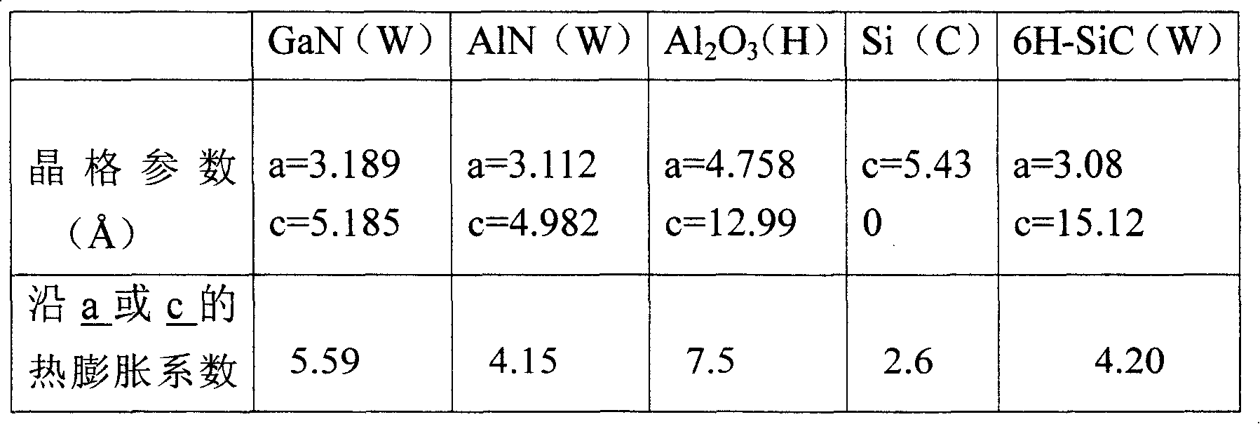

当期望用氮化镓形成工作层时,发明的方法是尤其有利的。为此,现有技术提出了存有缺陷的各种技术,而本发明克服了这些缺陷。The inventive method is particularly advantageous when it is desired to use gallium nitride to form the working layer. For this reason, the prior art proposes various techniques with deficiencies, and the present invention overcomes these deficiencies.
由此,在现有技术中,使用由单晶碳化硅或蓝宝石构成的衬底作为支撑以及作为工作层的生长籽晶。但是,当工作层用以形成发光二极管(LEDs)时,使用固体碳化硅或蓝宝石支撑意味着不能以满意的方式控制电接触的位置、提取由二极管发射的光或使用反射表面等。在这种情况下,可以选择适合于淀积操作并还可恢复的第一支撑,接着在除去适合于实现对上述方面更好控制的第一支撑之后,可选择适合的第二支撑。而且,由单晶碳化硅构成的衬底,和对于较小范围的蓝宝石,是昂贵的和是有限直径的,然而在本发明的情况中使用可以变薄和从任选地可重复利用的衬底或单晶取得的籽晶层,由此可以节约昂贵材料的消费。而且,例如本发明可使利用由比单晶碳化硅易于以大直径获得的材料构成的籽晶层成为可能。Thus, in the prior art, substrates made of single-crystal silicon carbide or sapphire are used as supports and as growth seeds for the working layers. However, when the working layers are used to form light-emitting diodes (LEDs), the use of solid silicon carbide or sapphire supports means that the position of electrical contacts, extraction of light emitted by the diodes, or the use of reflective surfaces cannot be controlled in a satisfactory manner. In this case, it is possible to select a first support that is suitable for the deposition operation and also recoverable, and then after removal of the first support that is suitable to achieve better control of the above-mentioned aspects, a suitable second support can be selected. Furthermore, substrates consisting of single crystal silicon carbide, and to a lesser extent sapphire, are expensive and of limited diameter, whereas in the case of the present invention the use of substrates which can be thinned and obtained from optionally reusable The seed layer obtained from the bottom or single crystal can thus save the consumption of expensive materials. Furthermore, for example, the present invention may make it possible to use a seed layer composed of a material that is more readily available in larger diameters than single crystal silicon carbide.
而且,蓝宝石是电绝缘体,因此如果以固体支撑的形式保留蓝宝石,那么对于需要用于工作层预期应用以单独地提供在工作层自身上的的任何电极,蓝宝石变得必须,其可能引起可利用空间(例如如果在前面上,即工作层的空闲表面上将制造两个电接触)的问题。Also, sapphire is an electrical insulator, so if retained in a solid supported form, it becomes necessary for any electrode required for the intended application of the working layer to be provided separately on the working layer itself, which may lead to the use of A matter of space (for example if two electrical contacts are to be made on the front, ie on the free surface of the working layer).
本发明使除去相关的希望用于形成工作层的生长籽晶的性质和用于支撑的性质成为可能,尤其是当消除具有重复利用可能性的支撑时,由此可以减轻上面提到的缺陷。The invention makes it possible to remove the properties associated with the growth seeds desired for the formation of the working layer and for the support, especially when eliminating the support with the possibility of reuse, thereby alleviating the above-mentioned drawbacks.
在其它现有技术中,试图在固体氮化镓或甚至钕镓盐酸上或铟镓盐酸上直接淀积氮化镓。但是,固体氮化镓非常昂贵并且那些技术也不成熟。In other prior art attempts have been made to deposit gallium nitride directly on solid gallium nitride or even on neodymium gallium hydrochloride or indium gallium hydrochloride. However, solid gallium nitride is very expensive and those technologies are immature.
在上述的其它现有技术中,在{111}硅上已经淀积了氮化镓工作层。但是,如果{111}硅用作支撑,即以厚的形式,那么由于在热膨胀方面的不良匹配在工作层中观察到破裂。通过除去相关选择,本发明首先使选择适合于晶核形成并足够薄以在热应力作用下变形的籽晶层成为可能,其次使选择在热膨胀方面与在籽晶层上引起生长的工作层匹配的厚层成为可能。In the other prior art mentioned above, a working layer of gallium nitride has been deposited on {111} silicon. However, if {111} silicon is used as a support, ie in thick form, cracks are observed in the working layer due to poor matching in terms of thermal expansion. By removing the relevant options, the invention firstly makes it possible to choose a seed layer suitable for nucleation and thin enough to deform under thermal stress, and secondly to make the choice match in terms of thermal expansion the working layer that induces growth on the seed layer thick layers possible.
有利地,发明的方法包括以下分别获得的特征或特征的结合:Advantageously, the inventive method comprises the following features or combinations of features obtained separately:
在籽晶层和支撑之间设置至少一个键合层,粘合界面包括该或每一键合层;at least one bonding layer is disposed between the seed layer and the support, the bonding interface comprising the or each bonding layer;
由取自下列的材料构成工作层,包括:氮化镓、氮化铝和氮化镓铝(而且总的来说,具有大的禁带宽度的半导体氮化物);The active layer is composed of materials taken from the group consisting of gallium nitride, aluminum nitride and aluminum gallium nitride (and in general, semiconductor nitrides with large bandgap widths);
籽晶层包括取自下列的材料,包括:蓝宝石、碳化硅、氧化锌和{111}硅;The seed layer includes materials from the following: sapphire, silicon carbide, zinc oxide, and {111} silicon;
选择籽晶层以获得精确的晶体结构和取向,例如获得六角形的或立方体的氮化镓,或者如果选择Si面或C面以在碳化硅的籽晶层上淀积工作层;Selection of the seed layer to obtain precise crystal structure and orientation, e.g. to obtain hexagonal or cubic GaN, or if Si face or C face is selected to deposit working layers on the seed layer of SiC;
由非常高质量的氮化镓构成籽晶层,即具有每平方厘米小于106位错,例如通过外延横向附生(ELOG)技术获得的氮化镓;The seed layer is made of very high-quality GaN, i.e. with less than 10 6 dislocations per square centimeter, such as GaN obtained by the epitaxial lateral epitaxy (ELOG) technique;
支撑包括取自下列的材料,包括:非晶材料、多晶材料和烧结材料;Supports include materials from the group consisting of: amorphous materials, polycrystalline materials, and sintered materials;
支撑包括取自下列的材料,包括:多晶碳化硅、单晶碳化硅、多晶氮化铝、多晶氮化镓和具有高位错浓度(大于107/cm2)的单晶氮化铝;Supports include materials taken from polycrystalline silicon carbide, single crystal silicon carbide, polycrystalline aluminum nitride, polycrystalline gallium nitride, and single crystal aluminum nitride with high dislocation concentration (greater than 10 7 /cm 2 ) ;
籽晶层是与支撑相同的化学成分;The seed layer is the same chemical composition as the support;
通过在预先削弱区从源衬底分离籽晶层,籽晶层取自源衬底;the seed layer is taken from the source substrate by separating the seed layer from the source substrate at the pre-weakened region;
籽晶层取自安置到支撑的源衬底并接着通过它的空闲表面被蚀刻以致获得所需厚度的籽晶层(为了该目的,可以利用取自用于获得衬底的技术和本领域已知的如键合和回刻蚀绝缘体上的硅(BESOI)的技术类型);The seed layer is taken from a source substrate placed on a support and then etched through its free surface so as to obtain a seed layer of the desired thickness (for this purpose it is possible to use techniques taken from techniques used to obtain substrates and known in the art known as bonding and etch-back silicon-on-insulator (BESOI) type);
通过在源衬底中相应于籽晶层的厚度(忽略完成的步骤)的深度注入原子粒种;和seeding atomic particles by implanting atomic particles at a depth in the source substrate corresponding to the thickness of the seed layer (ignoring the steps completed); and
通过取自下列的操作从源衬底至少部分地分离籽晶层,该列包括:热处理、施加机械应力和化学蚀刻,或这些操作至少两个的结合。The seed layer is at least partially detached from the source substrate by operations taken from the list comprising: thermal treatment, application of mechanical stress and chemical etching, or a combination of at least two of these operations.
在该文献的上述和其它部分中,“原子注入”用以覆盖使用原子或离子粒种并适合于把这些粒种注入到材料的任何轰击以获得材料中这些粒种的浓度最大值,所述最大值位于相对于轰击表面的确定深度。原子或离子粒种以分布在一最大值附近的能量被注入到材料中。使用离子束注入器、等离子体浸入式注入器等可将原子粒种注入到材料中。使用术语“原子或离子粒种”意为以离子、中子或分子形式的原子,或以原子或中子形式的分子,或甚至以离子或中子形式的不同原子或分子的组合。In the above and other parts of this document, "atom implantation" is used to cover any bombardment using atomic or ionic species and suitable for implanting these species into a material to obtain a maximum concentration of these species in the material, said The maximum is located at a defined depth relative to the bombardment surface. Atomic or ionic species are implanted into the material with energies distributed around a maximum. Atomic seeds can be implanted into materials using ion beam implanters, plasma immersion implanters, and the like. By the term "atomic or ionic species" is meant an atom in ion, neutron or molecular form, or a molecule in atom or neutron form, or even a combination of different atoms or molecules in ion or neutron form.
附图说明 Description of drawings
阅读以下详细的说明本发明的其它方面、目的和优点将更为清楚,且参照附图也将会更好地理解本发明,其中:Other aspects, objects and advantages of the present invention will become clearer upon reading the following detailed description, and the present invention will be better understood with reference to the accompanying drawings, wherein:
图1是示出根据发明方法实施例的步骤简图;Fig. 1 is a schematic diagram showing the steps of an embodiment of the method according to the invention;
图2是示出根据发明方法另一实施例的步骤简图;Fig. 2 is a schematic diagram illustrating the steps of another embodiment of the method according to the invention;
图3仍是发明方法实施例的步骤简图;和Fig. 3 is still a schematic diagram of the steps of the inventive method embodiment; and
图4是具有四个籽晶层的中间支撑、可以用在本发明方法的变形形式的示意透视图。Figure 4 is a schematic perspective view of a variant of an intermediate support with four seed layers, which can be used in the method of the invention.
具体实施方式 Detailed ways
以下参照四个具体但非限制性的实施例详细说明发明的方法。The method of the invention is described in detail below with reference to four specific but non-limiting examples.
在第一实施例中,如图1所示,通过实施以下的步骤制得包括在籽晶层2上的工作层16的最终衬底14:In the first embodiment, as shown in FIG. 1 , the final substrate 14 comprising a working
在其内须注入原子粒种的源衬底6的表面上形成非晶材料层以制得键合层10,在支撑12的表面上形成非晶材料层以制得另一键合层11;Forming an amorphous material layer on the surface of the
在源衬底6中确定的深度注入原子粒种以形成削弱区8;implanting atomic species at a defined depth in the
100,使键合层10和11接触;100, making
200,借助削弱区8从源衬底6分离籽晶层2;和200, separating the
300,在对应于削弱区8的籽晶层2的表面上淀积工作层16。300 , deposit a working
形成键合层10和以上述指定的次序进行或以另一次序进行注入原子类的步骤。。The steps of forming the
例如,法国专利第FR2681472号中说明了实施原子粒种的步骤和分离籽晶层2的步骤200实例。For example, French Patent No. FR2681472 describes an example of the step of performing atomic particle seeding and the
根据实例,形成键合层10和11的步骤相应于使用本领域技术人员公知的任何方法形成非晶材料层。According to an example, the step of forming
在步骤200和300之间,本发明的方法选择性地包括准备籽晶层2的表面的操作,籽晶层2的表面将接收工作层16。准备操作包括,例如,抛光操作、退火操作、精磨退火操作(例如在氢气下)、退火操作用于加固在键合层10和11之间的粘合界面、牺牲氧化操作(氧化之后接着为消除氧化材料)、蚀刻操作等。Between
下面五个依次描述的具体但非限制性的实例,详细地描述了本发明方法的第一实施例,通过这种方式,在实例5之后描述的实例中的粘合界面,进行分离。The following five specific but non-limiting examples, described in sequence, describe in detail a first embodiment of the method of the present invention, in this way, the bonded interface in the examples described after Example 5, is separated.
下表2概述了适合于用于实施上述第一实施例的材料的实例。Table 2 below summarizes examples of materials suitable for use in the practice of the first embodiment described above.
表2Table 2

在上表中,与在下表中一样,使用术语“单”意指“单晶”和使用术语“多”意指“多晶”。In the above table, as in the following table, the term "single" is used to mean "single crystal" and the term "poly" is used to mean "polycrystalline".
实例1Example 1
在相应于表2第一行的实例中,在由单晶碳化硅构成的籽晶层2上,工作层16由氮化镓构成,籽晶层自身在多晶碳化硅支撑12上,在支撑12和籽晶层2之间设置的碳化硅键合层10和11。In the example corresponding to the first row of Table 2, the working
通过实例,籽晶层2是1000
通过本领域技术人员公知的层迁移方法(例如,参见法国专利第FR2681472号中Smart-Cut
可以由化学汽相淀积(CVD)、高温化学汽相淀积(HTCVD)、MOCVD、MBE或氢化物汽相外延(HVPE)制得工作层16,例如参见文献“用于GaN基LEDs和LDs的GaN体衬底”,作者O.Oda等,Phys.Stat.Sol.(a),No.180,p51(2000),或其它等同的技术。The working
氧化硅用于键合层10使得易于从源衬底6取得籽晶层2。氧化硅的平面化淀积可能消除表面不均匀(irregularities)并可能使用易于实施的常规技术进行抛光步骤、平面化步骤、清洗步骤、化学准备步骤和把所述氧化硅键合到在支撑12上形成的键合层11的氧化硅上。根据实例,键合层10和11设置为1微米厚。The use of silicon oxide for the
实例2Example 2
在这个实例中(上表第2行),除了由{111}硅籽晶层2替代碳化硅籽晶层2之外,提供与实例1等同的结构。In this example (
{111}硅的厚度优选限制到小于3000
实例3Example 3
在这个实例中(上表第3行),除了由蓝宝石构成籽晶层2之外,制得与实例1和2的结构等同的结构。In this example (row 3 of the above table), a structure equivalent to that of Examples 1 and 2 was produced except that the
蓝宝石是使得氮化镓优良外延的公知的另一种材料。Sapphire is another material known to make excellent epitaxy of gallium nitride.
实例4Example 4
在这个实例中(上表第4行),除了由多晶氮化镓构成籽晶层2之外,制得与实例1至3的结构等同的结构。In this example (
实例5Example 5
在这个实例中(上表第5行),除了由钕镓酸盐或锂镓酸盐构成籽晶层2之外,制得与实例1至4的结构等同的结构。In this example (row 5 of the table above), a structure equivalent to that of Examples 1 to 4 was produced, except that the
可以联想到上述实例的多种变体。Numerous variations of the above example can be envisioned.
由此,可以由某些其它材料,例如氮化硅(Si3N4)替代键合层10和11之一中的氧化硅或两个键合层10和11中的氧化硅。这种材料可以比氧化硅承受更高的温度。为了形成高质量的多晶层或甚至当期望增加淀积速率时,在优化工作层16的淀积情况下,这种优点是尤其有利的。氮化硅还具有限制或甚至避免镓扩散到支撑12中的优点。The silicon oxide in one of the bonding layers 10 and 11 or the silicon oxide in both bonding layers 10 and 11 can thus be replaced by some other material, for example silicon nitride (Si 3 N 4 ). This material can withstand higher temperatures than silicon oxide. This advantage is particularly advantageous in the case of optimizing the deposition of the working
仍然在发明方法的该第一实施例的另一变体中,由氮化铝、碳化硅、铝合金和镓合金、和镓和铟的合金、或某些其它化合物的工作层16替代氮化镓工作层16。还可以由氮化镓、氮化铝、氮化镓铟等类型层的叠层构成的多层结构替代氮化镓工作层16,其可以具有不同的掺杂种类等。Still in another variant of this first embodiment of the inventive method, the nitriding is replaced by a working
仍然在另一变体中,由单晶碳化硅(尤其是当如下所述支撑12可以重复利用时)、蓝宝石、多晶氮化铝或多晶氮化镓替代多晶碳化硅支撑12。In yet another variant, the polycrystalline
在生长工作层16之后,可能在加固作为整体的结构之后(为了强度问题加固是必须的),借助于某另一个支撑通过直接粘合或通过在工作层上淀积支撑形成所述的另一个支撑等,除去支撑12。After growing the working
然后支撑12必须能够承受工作层16生长的条件,而且通过适合的除去是有利的。移开中间支撑12所选择的技术可以确定构成支撑所选择的材料。如果通过蚀刻或机械或化学除去将牺牲支撑,那么蚀刻和除去步骤还有中间支撑12自身必须是尽可能低成本。在这种情况下,支撑12应该由多晶氮化铝构成。The
分离separate
在发明中,使用例如机械、热、静电、激光辐射等应力引起组合体分离为位于粘合界面任一侧上的两部分。In the invention, the use of stress such as mechanical, thermal, electrostatic, laser radiation, etc. causes the assembly to separate into two parts on either side of the bonded interface.
在这种情况下,因为不被消耗并可以重复利用可以由单晶碳化硅构成支撑12。In this case, the
在另一变体中,在除去支撑12之前或之后制得在工作层16上的所有或某些部件。In another variant, all or some of the components on the working
在本发明方法如图2所示的第二实施例中,,制得与上述发明方法第一实施例中一样的结构,该结构包括籽晶层2上的工作层16,籽晶层自身在支撑12上,支撑12具有正在籽晶层2和支撑12之间设置的键合层10和11。接着,按照本实施例,在工作层16的空闲表面上淀积厚层4并除去支撑12,可以一同除去籽晶层2。在支撑12除去之后,厚层4特别地用于形成用于工作层16的支撑。In the second embodiment of the method of the present invention as shown in FIG. On the
下表3概括了在发明方法的该第二实施例的情况下可以使用的材料的实例。Table 3 below summarizes examples of materials that can be used in the context of this second embodiment of the inventive method.
表3table 3
实例6Example 6
在该实例中,在多晶碳化硅支撑12上制得单晶{111}硅籽晶层2,碳化硅支撑12具有在碳化硅支撑12和籽晶层2之间的氧化硅键合层10和11。其后,由MOCVD淀积单晶氮化镓工作层16,并在工作层16的单晶氮化镓空闲面上淀积金刚石厚层4。In this example, a monocrystalline {111}
其后最终的结构经受处理,该处理适合于从由支撑12和籽晶层2构成的组合体分离出由工作层16构成的部件。该处理包括使用机械、热、静电等应力使两部分分离在粘合界面的任一侧。The final structure is thereafter subjected to a treatment suitable for separating the component formed by the working
该实例表现出的优点为:可以使用在其表面不能很好完成接收籽晶层2的支撑12,但是一旦依靠{111}硅籽晶层2形成GaN工作层16,就可以制得用于工作层16的最终支撑(厚层4),该支撑具有适合于使用所述工作层16的性质(在这种情况下,对于金刚石,它具有好的热传导性和所需的,如用于微波应用的电绝缘性),还可以确保在厚层4和工作层16之间的高质量界面,例如以获得较好的热传导。This example presents the advantage that it is possible to use a
该实例可以包括多种变体。This example can include many variations.
由此,可以由单晶碳化硅、蓝宝石、钕镓酸盐或锂镓酸盐替代{111}硅籽晶层2;可以由氮化硅替代氧化硅键合层10和11;可以由多晶碳化硅或由蓝宝石替代多晶碳化硅支撑12;和可以由多晶碳化硅、多晶氮化镓(例如由HVPE淀积)、氮化硼或例如铜的金属等(例如由电解淀积作为厚层)替代金刚石厚层4。Thus, the {111}
应当注意到厚层4的厚度性质是重要的,例如当期望与最终衬底14的背面电接触时,或当必须能够疏散由在工作层16上制得的部件产生的热时,或甚至当期望提高由在工作层16中制得的二极管或激光器发射的光的提取或控制时。可以理解选择厚层4的性质在衬底制造方法中提供自由度,当制造用于光学器件、电子器件、光电器件等的衬底时自由度是尤其有利的。为了使厚层4随后能从工作层16分离,还可以通过提供准备步骤(其为本领域技术人员公知)在衬底制造方法中增加自由度。It should be noted that the nature of the thickness of the
相似地,这些变体可以改变,其中由氮化铝、碳化硅、铝和镓的合金或其它化合物构成工作层16,替代如上述用氮化镓制得工作层16。氮化镓工作层16还可以是层叠氮化镓、氮化铝等类型层的多层结构,可以具有不同种类的掺杂等。Similarly, these variations may be varied in which the working
在如图3所示的本发明方法的第三实施例中,与根据本发明的第二实施例上述说明相反,在工作层16和籽晶层2分离之后淀积厚层4制得结构。如果籽晶层2与支撑12一起除去或在除去支撑12之后除去,在所述籽晶层2上或在工作层16的相应面上,还可以在与工作层16的空闲面同一侧上淀积厚层4或可以在与籽晶层2的同一侧上淀积厚层4。In a third embodiment of the method according to the invention shown in FIG. 3 , contrary to what was described above according to the second embodiment of the invention, the structure is produced by depositing a
下面根据三个实例说明本发明方法的第三实施例。The third embodiment of the method of the present invention will be described below based on three examples.
表4中概括了这三个实施例中使用的材料,并且它们相应于表3的材料。The materials used in these three examples are summarized in Table 4 and correspond to those of Table 3.
表4Table 4
实例7Example 7
在该实例中(表4第1行),以与实例1的上述说明相同的方式,制得的结构包括:与上述描述的实例相同的方式,在单晶碳化硅支撑12上的单晶碳化硅籽晶层2,单晶碳化硅支撑12具有在多晶碳化硅支撑12和多晶碳化硅籽晶层2之间的氧化硅键合层10和11。其后,通过MOCVD在碳化硅籽晶层2的空闲表面上制得单晶氮化镓工作层16。以这种方式获得的结构接着经受处理,该处理适合于从支撑12分离由籽晶层2和工作层16构成的结构。这首先提供了由覆盖在单晶碳化硅的籽晶层2内的氮化镓工作层16构成的结构,和准备用于重复利用的支撑12。接着在籽晶层2上通过CVD淀积多晶碳化硅厚层4。In this example (Table 4, row 1), in the same manner as described above for Example 1, a structure was produced comprising: single crystal carbide on a single crystal
单晶碳化硅支撑12相对昂贵,但当实施随后的本发明的方法时,它可以重复利用。The monocrystalline
实例8Example 8
在发明方法的该第三实施例的另一实例中(表4第2行),制得与实例7相同的结构,但是在形成多晶碳化硅厚层4之前多晶碳化硅籽晶层2被移开,例如通过等离子体蚀刻。In another example of this third embodiment of the inventive method (Table 4, row 2), the same structure as in Example 7 is produced, but with the polycrystalline silicon
实例9Example 9
仍然在本发明方法的该第三实施例的另一个实例中(表4第3行),除了除去单晶碳化硅籽晶层2,和氮化镓工作层16的一部分以保存表现出尽可能少缺陷的工作层16,制得与实例8一样的结构。Still in another example of this third embodiment of the method of the invention (Table 4 row 3), in addition to removing the monocrystalline silicon
应当注意到在淀积厚层4之前,可以对单晶碳化硅籽晶层2或单晶氮化镓工作层16进行各种附加技术步骤,这些步骤试图提供某些或所有的电子部件,或包括外延地或其它方式制得附加膜的均匀淀积。It should be noted that prior to the deposition of the
应当注意到由选择用于初始源衬底6的极性可以确定单晶碳化硅籽晶层2的极性和氮化镓工作层16的极性。本发明的方法选择地包括至少一个双重迁移使得极性能够改变两次。It should be noted that the polarity of the monocrystalline silicon
相似地,按照本发明的这些实例可以改变,其中由氮化铝、碳化硅、铝和镓的合金、铟和镓的合金或某些其它化合物构成工作层16,替代如上述用氮化镓制得工作层16。氮化镓工作层16还可以是包括氮化镓、氮化铝等类型层的叠层的多层结构,其选择地具有不同掺杂种类等。Similarly, these examples according to the invention may be varied in which the working
籽晶层2可以由{111}硅或蓝宝石或钕镓酸盐或铟镓酸盐等构成,替代由单晶碳化硅构成。The
支撑12可以由多晶碳化硅或多晶氮化硅或多晶氮化铝或蓝宝石或多晶氮化镓构成,替代由单晶碳化硅构成。厚层4可以由多晶氮化铝、金刚石或氮化硼构成,替代由多晶碳化硅构成。The
在本发明方法的第四实施例中,除了没有制得中间层10和11之外,制得与上述实例一样的结构。例如,籽晶层2取自{111}硅源衬底6并通过直接粘合(例如与前述实施例一样)与多晶碳化硅12组合。其后,使用上述技术之一在籽晶层2上淀积氮化镓工作层16。In a fourth embodiment of the method of the present invention, the same structure as in the above example is produced except that the
不脱离本发明的范围还可以联想到对上述实施例的各种其它变体。Various other variants to the above-described embodiments are also conceivable without departing from the scope of the present invention.
例如,本发明方法实施例的不同实例中说明的操作可以彼此组合。For example, operations described in different instances of method embodiments of the present invention may be combined with each other.
如图4所示,一个变体在于:在淀积工作层16之前在籽晶层2上进行成批处理。在这种情况下,在大尺寸的常见支撑12上安置籽晶层2。As shown in FIG. 4 , a variant consists in performing a batch process on the
该常见支撑12的形状可以是任意的(圆形、矩形等)。The shape of this
在这些情况下,籽晶层2可以是同样的或它们可以是不同的。每个籽晶层2可以经受把籽晶层从支撑12分离的分离操作。按照实例,常见支撑12可以是由硅氧化物覆盖的多晶氮化硅板。In these cases, the seed layers 2 may be the same or they may be different. Each
有利地,在试图把在籽晶层2上的工作层组件16从支撑12分离的操作之前,将变硬的衬底键合到每个不同组件的工作层16。Advantageously, the stiffened substrate is bonded to each different assembly of the working
每个常见支撑12是重复利用的。Each
在发明方法的另一个变体中,优化控制厚层4淀积的参数以制得单晶的厚层4。In another variant of the inventive method, the parameters controlling the deposition of the
即使单晶厚层4不是最好的质量,它的质量仍然在许多应用中是足够的,仅对工作层16无论何时都需要非常高晶体质量。Even if the monocrystalline
当不能生长单晶(如氮化镓情况)时和当它们难于生长(如碳化硅情况)时本发明的方法时尤其有利的。The method of the invention is especially advantageous when single crystals cannot be grown (as in the case of gallium nitride) and when they are difficult to grow (as in the case of silicon carbide).
在其它变体中,上述说明可以进行变化,用其它半导体材料生长工作层,例如磷化铟、砷化镓、锗、硅-锗等,或甚至其它材料,例如铌酸锂。In other variants, the above description can be varied to grow the working layer with other semiconductor materials, such as indium phosphide, gallium arsenide, germanium, silicon-germanium, etc., or even other materials, such as lithium niobate.
仍在另一变体中,不使用键合层10或11,或仅使用一个这样的层(在支撑12上或在籽晶层2上)。In yet another variant, no
仍在另一变体中,在工作层16和/或籽晶层2(如果它是保存的)与支撑12或厚层4之间制得中间层,例如绝缘层,以形成包括在绝缘材料上半导体的衬底。按照实例,中间层可以由金刚石、优良的氧化物(500厚)等构成。In yet another variant, an intermediate layer, such as an insulating layer, is made between the working
Claims (16)
Applications Claiming Priority (2)
| Application Number | Priority Date | Filing Date | Title |
|---|---|---|---|
| FR0015279A FR2817394B1 (en) | 2000-11-27 | 2000-11-27 | METHOD FOR MANUFACTURING A SUBSTRATE, IN PARTICULAR FOR OPTICS, ELECTRONICS OR OPTOELECTRONICS AND SUBSTRATE OBTAINED THEREBY |
| FR00/15279 | 2000-11-27 |
Related Parent Applications (1)
| Application Number | Title | Priority Date | Filing Date |
|---|---|---|---|
| CN018196071A Division CN1217381C (en) | 2000-11-27 | 2001-11-26 | Compound semiconductor substrate and manufacturing method thereof |
Publications (2)
| Publication Number | Publication Date |
|---|---|
| CN1734718A CN1734718A (en) | 2006-02-15 |
| CN100399511C true CN100399511C (en) | 2008-07-02 |
Family
ID=8856906
Family Applications (2)
| Application Number | Title | Priority Date | Filing Date |
|---|---|---|---|
| CN018196071A Expired - Lifetime CN1217381C (en) | 2000-11-27 | 2001-11-26 | Compound semiconductor substrate and manufacturing method thereof |
| CNB2005100842833A Expired - Lifetime CN100399511C (en) | 2000-11-27 | 2001-11-26 | Compound semiconductor substrate and manufacturing method thereof |
Family Applications Before (1)
| Application Number | Title | Priority Date | Filing Date |
|---|---|---|---|
| CN018196071A Expired - Lifetime CN1217381C (en) | 2000-11-27 | 2001-11-26 | Compound semiconductor substrate and manufacturing method thereof |
Country Status (11)
| Country | Link |
|---|---|
| US (2) | US6794276B2 (en) |
| EP (2) | EP1791170B1 (en) |
| JP (2) | JP2004517472A (en) |
| KR (1) | KR100805469B1 (en) |
| CN (2) | CN1217381C (en) |
| AT (2) | ATE427559T1 (en) |
| AU (1) | AU2002222036A1 (en) |
| DE (2) | DE60126328T2 (en) |
| FR (1) | FR2817394B1 (en) |
| TW (1) | TW536728B (en) |
| WO (1) | WO2002043112A2 (en) |
Cited By (1)
| Publication number | Priority date | Publication date | Assignee | Title |
|---|---|---|---|---|
| CN103988285A (en) * | 2011-12-13 | 2014-08-13 | 索泰克公司 | Process for stabilizing bonding interface located within structure comprising oxide layer, and the structure obtained |
Families Citing this family (163)
| Publication number | Priority date | Publication date | Assignee | Title |
|---|---|---|---|---|
| US7560296B2 (en) * | 2000-07-07 | 2009-07-14 | Lumilog | Process for producing an epitalixal layer of galium nitride |
| US7118929B2 (en) * | 2000-07-07 | 2006-10-10 | Lumilog | Process for producing an epitaxial layer of gallium nitride |
| US8507361B2 (en) | 2000-11-27 | 2013-08-13 | Soitec | Fabrication of substrates with a useful layer of monocrystalline semiconductor material |
| FR2840730B1 (en) * | 2002-06-11 | 2005-05-27 | Soitec Silicon On Insulator | METHOD FOR MANUFACTURING A SUBSTRATE COMPRISING A LAYER UTILIZED IN MONOCRYSTALLINE SEMICONDUCTOR MATERIAL WITH IMPROVED PROPERTIES |
| FR2894990B1 (en) | 2005-12-21 | 2008-02-22 | Soitec Silicon On Insulator | PROCESS FOR PRODUCING SUBSTRATES, IN PARTICULAR FOR OPTICS, ELECTRONICS OR OPTOELECTRONICS AND SUBSTRATE OBTAINED BY SAID PROCESS |
| US7407869B2 (en) | 2000-11-27 | 2008-08-05 | S.O.I.Tec Silicon On Insulator Technologies | Method for manufacturing a free-standing substrate made of monocrystalline semiconductor material |
| FR2817394B1 (en) * | 2000-11-27 | 2003-10-31 | Soitec Silicon On Insulator | METHOD FOR MANUFACTURING A SUBSTRATE, IN PARTICULAR FOR OPTICS, ELECTRONICS OR OPTOELECTRONICS AND SUBSTRATE OBTAINED THEREBY |
| FR2840731B3 (en) | 2002-06-11 | 2004-07-30 | Soitec Silicon On Insulator | METHOD FOR MANUFACTURING A SUBSTRATE HAVING A USEFUL LAYER OF SINGLE-CRYSTAL SEMICONDUCTOR MATERIAL OF IMPROVED PROPERTIES |
| FR2835096B1 (en) * | 2002-01-22 | 2005-02-18 | PROCESS FOR MANUFACTURING SELF-CARRIER SUBSTRATE OF SINGLE-CRYSTALLINE SEMICONDUCTOR MATERIAL | |
| EP1386349A1 (en) | 2001-04-17 | 2004-02-04 | California Institute Of Technology | A method of using a germanium layer transfer to si for photovoltaic applications and heterostructure made thereby |
| US7238622B2 (en) * | 2001-04-17 | 2007-07-03 | California Institute Of Technology | Wafer bonded virtual substrate and method for forming the same |
| US20050026432A1 (en) * | 2001-04-17 | 2005-02-03 | Atwater Harry A. | Wafer bonded epitaxial templates for silicon heterostructures |
| US6770966B2 (en) * | 2001-07-31 | 2004-08-03 | Intel Corporation | Electronic assembly including a die having an integrated circuit and a layer of diamond to transfer heat |
| FR2835095B1 (en) * | 2002-01-22 | 2005-03-18 | PROCESS FOR PREPARING SEPARABLE SEMICONDUCTOR ASSEMBLIES, IN PARTICULAR FOR FORMING SUBSTRATES FOR ELECTRONICS, OPTOELECTRIC, AND OPTICS | |
| FR2840452B1 (en) * | 2002-05-28 | 2005-10-14 | Lumilog | PROCESS FOR THE EPITAXIC PRODUCTION OF A GALLIUM NITRIDE FILM SEPARATED FROM ITS SUBSTRATE |
| US6936497B2 (en) * | 2002-12-24 | 2005-08-30 | Intel Corporation | Method of forming electronic dies wherein each die has a layer of solid diamond |
| US7018909B2 (en) * | 2003-02-28 | 2006-03-28 | S.O.I.Tec Silicon On Insulator Technologies S.A. | Forming structures that include a relaxed or pseudo-relaxed layer on a substrate |
| DE60336543D1 (en) | 2003-05-27 | 2011-05-12 | Soitec Silicon On Insulator | Process for producing a heteroepitaxial microstructure |
| FR2855909B1 (en) * | 2003-06-06 | 2005-08-26 | Soitec Silicon On Insulator | PROCESS FOR THE CONCURRENT PRODUCTION OF AT LEAST ONE PAIR OF STRUCTURES COMPRISING AT LEAST ONE USEFUL LAYER REPORTED ON A SUBSTRATE |
| FR2855908B1 (en) * | 2003-06-06 | 2005-08-26 | Soitec Silicon On Insulator | METHOD FOR OBTAINING A STRUCTURE COMPRISING AT LEAST ONE SUBSTRATE AND AN ULTRAMINO LAYER |
| TWI240434B (en) | 2003-06-24 | 2005-09-21 | Osram Opto Semiconductors Gmbh | Method to produce semiconductor-chips |
| US7015117B2 (en) * | 2003-07-14 | 2006-03-21 | Allegis Technologies, Inc. | Methods of processing of gallium nitride |
| FR2857982B1 (en) * | 2003-07-24 | 2007-05-18 | Soitec Silicon On Insulator | PROCESS FOR PRODUCING AN EPITAXIC LAYER |
| US7538010B2 (en) | 2003-07-24 | 2009-05-26 | S.O.I.Tec Silicon On Insulator Technologies | Method of fabricating an epitaxially grown layer |
| FR2857983B1 (en) | 2003-07-24 | 2005-09-02 | Soitec Silicon On Insulator | PROCESS FOR PRODUCING AN EPITAXIC LAYER |
| FR2868204B1 (en) * | 2004-03-25 | 2006-06-16 | Commissariat Energie Atomique | SEMICONDUCTOR-TYPE SUBSTRATE ON INSULATION COMPRISING A CARBON DIAMOND BURIED LAYER |
| US20080211061A1 (en) * | 2004-04-21 | 2008-09-04 | California Institute Of Technology | Method For the Fabrication of GaAs/Si and Related Wafer Bonded Virtual Substrates |
| US9011598B2 (en) * | 2004-06-03 | 2015-04-21 | Soitec | Method for making a composite substrate and composite substrate according to the method |
| WO2006015185A2 (en) * | 2004-07-30 | 2006-02-09 | Aonex Technologies, Inc. | GaInP/GaAs/Si TRIPLE JUNCTION SOLAR CELL ENABLED BY WAFER BONDING AND LAYER TRANSFER |
| US7579621B2 (en) | 2004-09-17 | 2009-08-25 | Massachusetts Institute Of Technology | Integrated BST microwave tunable devices using buffer layer transfer method |
| US7713839B2 (en) * | 2004-10-06 | 2010-05-11 | Intel Corporation | Diamond substrate formation for electronic assemblies |
| US7846759B2 (en) * | 2004-10-21 | 2010-12-07 | Aonex Technologies, Inc. | Multi-junction solar cells and methods of making same using layer transfer and bonding techniques |
| ATE420461T1 (en) * | 2004-11-09 | 2009-01-15 | Soitec Silicon On Insulator | METHOD FOR PRODUCING COMPOSITE WAFERS |
| DE102004062290A1 (en) * | 2004-12-23 | 2006-07-06 | Osram Opto Semiconductors Gmbh | Method for producing a semiconductor chip |
| EP1681712A1 (en) * | 2005-01-13 | 2006-07-19 | S.O.I. Tec Silicon on Insulator Technologies S.A. | Method of producing substrates for optoelectronic applications |
| JP2006210660A (en) * | 2005-01-28 | 2006-08-10 | Hitachi Cable Ltd | Manufacturing method of semiconductor substrate |
| US10374120B2 (en) * | 2005-02-18 | 2019-08-06 | Koninklijke Philips N.V. | High efficiency solar cells utilizing wafer bonding and layer transfer to integrate non-lattice matched materials |
| US8674405B1 (en) * | 2005-04-13 | 2014-03-18 | Element Six Technologies Us Corporation | Gallium—nitride-on-diamond wafers and devices, and methods of manufacture |
| JP2008537341A (en) * | 2005-04-13 | 2008-09-11 | ザ リージェンツ オブ ザ ユニバーシティ オブ カリフォルニア | Wafer separation technology for self-standing (Al, In, Ga) N wafer fabrication |
| US7595507B2 (en) * | 2005-04-13 | 2009-09-29 | Group4 Labs Llc | Semiconductor devices having gallium nitride epilayers on diamond substrates |
| TW200707799A (en) * | 2005-04-21 | 2007-02-16 | Aonex Technologies Inc | Bonded intermediate substrate and method of making same |
| KR100588377B1 (en) * | 2005-05-10 | 2006-06-09 | 삼성전기주식회사 | Vertical structure gallium nitride-based light emitting diode device and manufacturing method thereof |
| US20060284167A1 (en) * | 2005-06-17 | 2006-12-21 | Godfrey Augustine | Multilayered substrate obtained via wafer bonding for power applications |
| US7795050B2 (en) * | 2005-08-12 | 2010-09-14 | Samsung Electronics Co., Ltd. | Single-crystal nitride-based semiconductor substrate and method of manufacturing high-quality nitride-based light emitting device by using the same |
| US8334155B2 (en) * | 2005-09-27 | 2012-12-18 | Philips Lumileds Lighting Company Llc | Substrate for growing a III-V light emitting device |
| US20070069225A1 (en) * | 2005-09-27 | 2007-03-29 | Lumileds Lighting U.S., Llc | III-V light emitting device |
| US7568412B2 (en) * | 2005-10-04 | 2009-08-04 | Marquip, Llc | Method for order transition on a plunge slitter |
| JP2007180142A (en) * | 2005-12-27 | 2007-07-12 | Toshiba Corp | Nitride-based semiconductor device and manufacturing method thereof |
| US20070194342A1 (en) * | 2006-01-12 | 2007-08-23 | Kinzer Daniel M | GaN SEMICONDUCTOR DEVICE AND PROCESS EMPLOYING GaN ON THIN SAPHIRE LAYER ON POLYCRYSTALLINE SILICON CARBIDE |
| FR2896619B1 (en) * | 2006-01-23 | 2008-05-23 | Soitec Silicon On Insulator | PROCESS FOR MANUFACTURING A COMPOSITE SUBSTRATE WITH IMPROVED ELECTRIC PROPERTIES |
| JP4756418B2 (en) * | 2006-02-28 | 2011-08-24 | 公立大学法人大阪府立大学 | Method for manufacturing single crystal gallium nitride substrate |
| US8438119B2 (en) * | 2006-03-30 | 2013-05-07 | Sap Ag | Foundation layer for services based enterprise software architecture |
| US20070232074A1 (en) * | 2006-03-31 | 2007-10-04 | Kramadhati Ravi | Techniques for the synthesis of dense, high-quality diamond films using a dual seeding approach |
| US20070243703A1 (en) * | 2006-04-14 | 2007-10-18 | Aonex Technololgies, Inc. | Processes and structures for epitaxial growth on laminate substrates |
| JP5180189B2 (en) * | 2006-04-25 | 2013-04-10 | ナショナル ユニヴァーシティー オブ シンガポール | Method of zinc oxide film growth on epitaxial laterally abnormally grown gallium nitride templates |
| TW200802544A (en) | 2006-04-25 | 2008-01-01 | Osram Opto Semiconductors Gmbh | Composite substrate and method for making the same |
| US7498191B2 (en) * | 2006-05-22 | 2009-03-03 | Chien-Min Sung | Semiconductor-on-diamond devices and associated methods |
| US7670928B2 (en) * | 2006-06-14 | 2010-03-02 | Intel Corporation | Ultra-thin oxide bonding for S1 to S1 dual orientation bonding |
| US20080048192A1 (en) * | 2006-08-22 | 2008-02-28 | Chien-Min Sung | LED devices and associated methods |
| EP1901345A1 (en) * | 2006-08-30 | 2008-03-19 | Siltronic AG | Multilayered semiconductor wafer and process for manufacturing the same |
| US8236594B2 (en) * | 2006-10-20 | 2012-08-07 | Chien-Min Sung | Semiconductor-on-diamond devices and associated methods |
| WO2008091910A2 (en) * | 2007-01-22 | 2008-07-31 | Group4 Labs, Llc | Composite wafers having bulk-quality semiconductor layers |
| ATE518241T1 (en) * | 2007-01-24 | 2011-08-15 | Soitec Silicon On Insulator | PRODUCTION PROCESS FOR SILICON WAFER ON INSULATOR AND CORRESPONDING WAFER |
| US8157914B1 (en) * | 2007-02-07 | 2012-04-17 | Chien-Min Sung | Substrate surface modifications for compositional gradation of crystalline materials and associated products |
| US7732301B1 (en) | 2007-04-20 | 2010-06-08 | Pinnington Thomas Henry | Bonded intermediate substrate and method of making same |
| EP1986229A1 (en) * | 2007-04-27 | 2008-10-29 | S.O.I.T.E.C. Silicon on Insulator Technologies | Method for manufacturing compound material wafer and corresponding compound material wafer |
| US7799600B2 (en) * | 2007-05-31 | 2010-09-21 | Chien-Min Sung | Doped diamond LED devices and associated methods |
| US7781256B2 (en) * | 2007-05-31 | 2010-08-24 | Chien-Min Sung | Semiconductor-on-diamond devices and associated methods |
| FR2917232B1 (en) * | 2007-06-06 | 2009-10-09 | Soitec Silicon On Insulator | PROCESS FOR MANUFACTURING A STRUCTURE FOR EPITAXY WITHOUT EXCLUSION AREA |
| US20090278233A1 (en) * | 2007-07-26 | 2009-11-12 | Pinnington Thomas Henry | Bonded intermediate substrate and method of making same |
| KR101374090B1 (en) * | 2007-07-26 | 2014-03-17 | 아리조나 보드 오브 리젠츠 퍼 앤 온 비하프 오브 아리조나 스테이트 유니버시티 | Epitaxial methods and templates grown by the methods |
| WO2009015337A1 (en) * | 2007-07-26 | 2009-01-29 | S.O.I.Tec Silicon On Insulator Technologies | Methods for producing improved epitaxial materials |
| JP2009141093A (en) * | 2007-12-06 | 2009-06-25 | Toshiba Corp | Light emitting device and method for manufacturing light emitting device |
| FR2926674B1 (en) * | 2008-01-21 | 2010-03-26 | Soitec Silicon On Insulator | METHOD FOR MANUFACTURING COMPOSITE STRUCTURE WITH STABLE BONDING OXIDE LAYER |
| CN101521155B (en) * | 2008-02-29 | 2012-09-12 | 信越化学工业株式会社 | Method for preparing substrate having monocrystalline film |
| US7749884B2 (en) * | 2008-05-06 | 2010-07-06 | Astrowatt, Inc. | Method of forming an electronic device using a separation-enhancing species |
| FR2931293B1 (en) * | 2008-05-15 | 2010-09-03 | Soitec Silicon On Insulator | PROCESS FOR MANUFACTURING AN EPITAXIA SUPPORT HETEROSTRUCTURE AND CORRESPONDING HETEROSTRUCTURE |
| EP2294607A2 (en) * | 2008-05-17 | 2011-03-16 | Astrowatt, Inc. | Method of forming an electronic device using a separation technique |
| JP5548395B2 (en) * | 2008-06-25 | 2014-07-16 | 株式会社半導体エネルギー研究所 | Method for manufacturing SOI substrate |
| TWI457984B (en) | 2008-08-06 | 2014-10-21 | S O I Tec絕緣層上矽科技公司 | Strain layer relaxation method |
| EP2151852B1 (en) * | 2008-08-06 | 2020-01-15 | Soitec | Relaxation and transfer of strained layers |
| EP2151861A1 (en) * | 2008-08-06 | 2010-02-10 | S.O.I. TEC Silicon | Passivation of etched semiconductor structures |
| FR2934925B1 (en) * | 2008-08-06 | 2011-02-25 | Soitec Silicon On Insulator | METHOD FOR MANUFACTURING A STRUCTURE COMPRISING A STEP OF ION IMPLANTATIONS TO STABILIZE THE BONDING INTERFACE. |
| EP2151856A1 (en) * | 2008-08-06 | 2010-02-10 | S.O.I. TEC Silicon | Relaxation of strained layers |
| EP2159836B1 (en) * | 2008-08-25 | 2017-05-31 | Soitec | Stiffening layers for the relaxation of strained layers |
| WO2010025218A2 (en) * | 2008-08-28 | 2010-03-04 | The Regents Of The University Of California | Composite semiconductor substrates for thin-film device layer transfer |
| US8692260B2 (en) * | 2008-09-26 | 2014-04-08 | Soitec | Method of forming a composite laser substrate |
| US8048754B2 (en) * | 2008-09-29 | 2011-11-01 | Semiconductor Energy Laboratory Co., Ltd. | Method for manufacturing SOI substrate and method for manufacturing single crystal semiconductor layer |
| JP5611571B2 (en) * | 2008-11-27 | 2014-10-22 | 株式会社半導体エネルギー研究所 | Method for manufacturing semiconductor substrate and method for manufacturing semiconductor device |
| US7927975B2 (en) | 2009-02-04 | 2011-04-19 | Micron Technology, Inc. | Semiconductor material manufacture |
| FR2943174B1 (en) | 2009-03-12 | 2011-04-15 | Soitec Silicon On Insulator | ADAPTATION OF THE MESH PARAMETER OF A LAYER OF CONTAMINATED MATERIAL |
| US8633097B2 (en) | 2009-06-09 | 2014-01-21 | International Business Machines Corporation | Single-junction photovoltaic cell |
| US8802477B2 (en) * | 2009-06-09 | 2014-08-12 | International Business Machines Corporation | Heterojunction III-V photovoltaic cell fabrication |
| US20110048517A1 (en) * | 2009-06-09 | 2011-03-03 | International Business Machines Corporation | Multijunction Photovoltaic Cell Fabrication |
| US8703521B2 (en) * | 2009-06-09 | 2014-04-22 | International Business Machines Corporation | Multijunction photovoltaic cell fabrication |
| US20100310775A1 (en) * | 2009-06-09 | 2010-12-09 | International Business Machines Corporation | Spalling for a Semiconductor Substrate |
| US9520856B2 (en) | 2009-06-24 | 2016-12-13 | Avago Technologies General Ip (Singapore) Pte. Ltd. | Acoustic resonator structure having an electrode with a cantilevered portion |
| US9847243B2 (en) | 2009-08-27 | 2017-12-19 | Corning Incorporated | Debonding a glass substrate from carrier using ultrasonic wave |
| JP5377212B2 (en) | 2009-10-13 | 2013-12-25 | 信越化学工業株式会社 | Method for producing single crystal diamond substrate |
| US9847768B2 (en) * | 2009-11-23 | 2017-12-19 | Avago Technologies General Ip (Singapore) Pte. Ltd. | Polarity determining seed layer and method of fabricating piezoelectric materials with specific C-axis |
| DE102009057020B4 (en) | 2009-12-03 | 2021-04-29 | Solaero Technologies Corp. | Growth substrates for inverted metamorphic multijunction solar cells |
| EP2330697A1 (en) * | 2009-12-07 | 2011-06-08 | S.O.I.Tec Silicon on Insulator Technologies | Semiconductor device having an InGaN layer |
| US9012253B2 (en) * | 2009-12-16 | 2015-04-21 | Micron Technology, Inc. | Gallium nitride wafer substrate for solid state lighting devices, and associated systems and methods |
| JP5643509B2 (en) * | 2009-12-28 | 2014-12-17 | 信越化学工業株式会社 | SOS substrate manufacturing method with reduced stress |
| US8648387B2 (en) * | 2009-12-30 | 2014-02-11 | Industrial Technology Research Institute | Nitride semiconductor template and method of manufacturing the same |
| TW201133945A (en) * | 2010-01-12 | 2011-10-01 | jian-min Song | Diamond LED devices and associated methods |
| US8203153B2 (en) | 2010-01-15 | 2012-06-19 | Koninklijke Philips Electronics N.V. | III-V light emitting device including a light extracting structure |
| US8105852B2 (en) * | 2010-01-15 | 2012-01-31 | Koninklijke Philips Electronics N.V. | Method of forming a composite substrate and growing a III-V light emitting device over the composite substrate |
| US8154052B2 (en) | 2010-05-06 | 2012-04-10 | Koninklijke Philips Electronics N.V. | Light emitting device grown on wavelength converting substrate |
| US8536022B2 (en) | 2010-05-19 | 2013-09-17 | Koninklijke Philips N.V. | Method of growing composite substrate using a relaxed strained layer |
| US8692261B2 (en) | 2010-05-19 | 2014-04-08 | Koninklijke Philips N.V. | Light emitting device grown on a relaxed layer |
| JP2011254051A (en) * | 2010-06-04 | 2011-12-15 | Sumitomo Electric Ind Ltd | Silicon carbide substrate manufacturing method, semiconductor device manufacturing method, silicon carbide substrate and semiconductor device |
| FR2961948B1 (en) * | 2010-06-23 | 2012-08-03 | Soitec Silicon On Insulator | PROCESS FOR TREATING A COMPOUND MATERIAL PART |
| JP5468528B2 (en) * | 2010-06-28 | 2014-04-09 | 信越化学工業株式会社 | SUBSTRATE FOR GROWING SINGLE CRYSTAL DIAMOND, METHOD FOR PRODUCING THE SAME, AND METHOD FOR PRODUCING SINGLE CRYSTAL DIAMOND SUBSTRATE |
| CN103262210B (en) * | 2010-09-10 | 2017-09-08 | 维尔雷思科技有限公司 | The device that the method for electrooptical device is manufactured using the layer separated with semiconductor donor and is made up of this method |
| JP2012089828A (en) * | 2010-09-22 | 2012-05-10 | Toshiba Corp | Semiconductor device manufacturing method |
| GB2484506A (en) * | 2010-10-13 | 2012-04-18 | Univ Warwick | Heterogrowth |
| DE102011012298A1 (en) * | 2010-12-28 | 2012-06-28 | Osram Opto Semiconductors Gmbh | Composite substrate, composite substrate semiconductor chip and method of manufacturing composite substrates and semiconductor chips |
| US9082948B2 (en) | 2011-02-03 | 2015-07-14 | Soitec | Methods of fabricating semiconductor structures using thermal spray processes, and semiconductor structures fabricated using such methods |
| US9142412B2 (en) | 2011-02-03 | 2015-09-22 | Soitec | Semiconductor devices including substrate layers and overlying semiconductor layers having closely matching coefficients of thermal expansion, and related methods |
| US8436363B2 (en) | 2011-02-03 | 2013-05-07 | Soitec | Metallic carrier for layer transfer and methods for forming the same |
| US9203374B2 (en) | 2011-02-28 | 2015-12-01 | Avago Technologies General Ip (Singapore) Pte. Ltd. | Film bulk acoustic resonator comprising a bridge |
| US9099983B2 (en) | 2011-02-28 | 2015-08-04 | Avago Technologies General Ip (Singapore) Pte. Ltd. | Bulk acoustic wave resonator device comprising a bridge in an acoustic reflector |
| US9425764B2 (en) | 2012-10-25 | 2016-08-23 | Avago Technologies General Ip (Singapore) Pte. Ltd. | Accoustic resonator having composite electrodes with integrated lateral features |
| US9444426B2 (en) | 2012-10-25 | 2016-09-13 | Avago Technologies General Ip (Singapore) Pte. Ltd. | Accoustic resonator having integrated lateral feature and temperature compensation feature |
| JP2012230969A (en) * | 2011-04-25 | 2012-11-22 | Sumitomo Electric Ind Ltd | GaN-BASED SEMICONDUCTOR DEVICE MANUFACTURING METHOD |
| JP2013001624A (en) * | 2011-06-21 | 2013-01-07 | Sumitomo Electric Ind Ltd | Group iii nitride composite substrate, and evaluation method thereof |
| FR2977069B1 (en) | 2011-06-23 | 2014-02-07 | Soitec Silicon On Insulator | METHOD FOR MANUFACTURING A SEMICONDUCTOR STRUCTURE USING TEMPORARY COLLAGE |
| RU2469433C1 (en) * | 2011-07-13 | 2012-12-10 | Юрий Георгиевич Шретер | Method for laser separation of epitaxial film or layer of epitaxial film from growth substrate of epitaxial semiconductor structure (versions) |
| US8922302B2 (en) | 2011-08-24 | 2014-12-30 | Avago Technologies General Ip (Singapore) Pte. Ltd. | Acoustic resonator formed on a pedestal |
| US8383460B1 (en) * | 2011-09-23 | 2013-02-26 | GlobalFoundries, Inc. | Method for fabricating through substrate vias in semiconductor substrate |
| JP5903818B2 (en) * | 2011-09-26 | 2016-04-13 | 富士通株式会社 | Compound semiconductor device and manufacturing method thereof |
| US8476629B2 (en) * | 2011-09-27 | 2013-07-02 | Taiwan Semiconductor Manufacturing Company, Ltd. | Enhanced wafer test line structure |
| US9608592B2 (en) | 2014-01-21 | 2017-03-28 | Avago Technologies General Ip (Singapore) Pte. Ltd. | Film bulk acoustic wave resonator (FBAR) having stress-relief |
| US9359693B2 (en) | 2012-02-29 | 2016-06-07 | Element Six Technologies Us Corporation | Gallium-nitride-on-diamond wafers and manufacturing equipment and methods of manufacture |
| EP2645428A1 (en) * | 2012-03-28 | 2013-10-02 | Soitec | Manufacture of multijuntion solar cell devices |
| FR2992464B1 (en) * | 2012-06-26 | 2015-04-03 | Soitec Silicon On Insulator | METHOD FOR TRANSFERRING A LAYER |
| JP6042994B2 (en) * | 2012-10-26 | 2016-12-14 | アールエフエイチアイシー コーポレイション | Semiconductor device with improved reliability and operating life and method for manufacturing the same |
| CN105051919A (en) | 2013-01-16 | 2015-11-11 | Qmat股份有限公司 | Techniques for forming optoelectronic devices |
| JP6146111B2 (en) * | 2013-04-26 | 2017-06-14 | 株式会社豊田自動織機 | Semiconductor substrate manufacturing method and semiconductor substrate |
| US9553183B2 (en) * | 2013-06-19 | 2017-01-24 | Infineon Technologies Austria Ag | Gate stack for normally-off compound semiconductor transistor |
| FR3007891B1 (en) * | 2013-06-28 | 2016-11-25 | Soitec Silicon On Insulator | METHOD FOR MANUFACTURING A COMPOSITE STRUCTURE |
| US9064789B2 (en) * | 2013-08-12 | 2015-06-23 | International Business Machines Corporation | Bonded epitaxial oxide structures for compound semiconductor on silicon substrates |
| EP2933824B1 (en) * | 2014-04-14 | 2021-08-18 | Nxp B.V. | Substrate arrangement |
| FR3039003B1 (en) | 2015-07-17 | 2017-07-28 | Soitec Silicon On Insulator | PROCESS FOR PRODUCING A SUBSTRATE |
| JP2017059598A (en) * | 2015-09-14 | 2017-03-23 | 株式会社東芝 | Wafer and semiconductor device |
| JP6515757B2 (en) * | 2015-09-15 | 2019-05-22 | 信越化学工業株式会社 | Method of manufacturing SiC composite substrate |
| CN105420812B (en) * | 2015-09-16 | 2019-02-05 | 新疆天科合达蓝光半导体有限公司 | Method for stripping silicon carbide seed crystal from seed crystal support |
| JP2017079090A (en) * | 2015-10-22 | 2017-04-27 | 株式会社東芝 | Magnetic recording medium, and magnetic record reproducing apparatus |
| DE102019102323A1 (en) * | 2018-02-02 | 2019-08-08 | Infineon Technologies Ag | Wafer composite and method for the production of semiconductor components |
| FR3079532B1 (en) * | 2018-03-28 | 2022-03-25 | Soitec Silicon On Insulator | METHOD FOR MANUFACTURING A MONOCRYSTALLINE LAYER OF AIN MATERIAL AND SUBSTRATE FOR GROWTH BY EPITAXIS OF A MONOCRYSTALLINE LAYER OF AIN MATERIAL |
| FR3079534B1 (en) | 2018-03-28 | 2022-03-18 | Soitec Silicon On Insulator | METHOD FOR MANUFACTURING A MONOCRYSTALLINE LAYER OF GAAS MATERIAL AND SUBSTRATE FOR GROWTH BY EPITAXIS OF A MONOCRYSTALLINE LAYER OF GAAS MATERIAL |
| DE102019114328B4 (en) | 2018-05-31 | 2022-03-03 | Rohm Co. Ltd | SEMICONDUCTOR SUBSTRATE STRUCTURE AND POWER SEMICONDUCTOR DEVICE |
| US20220181210A1 (en) * | 2019-03-12 | 2022-06-09 | The Regents Of The University Of California | Method for removing a bar of one or more devices using supporting plates |
| JP7204625B2 (en) * | 2019-07-25 | 2023-01-16 | 信越化学工業株式会社 | Group III compound substrate manufacturing method and substrate manufactured by the manufacturing method |
| US11652146B2 (en) | 2020-02-07 | 2023-05-16 | Rfhic Corporation | Method of forming a semiconductor wafer containing a gallium-nitride layer and two diamond layers |
| CN113972128A (en) * | 2020-07-23 | 2022-01-25 | 乂馆信息科技(上海)有限公司 | Preparation method of self-supporting substrate |
| FR3114912B1 (en) * | 2020-10-06 | 2022-09-02 | Soitec Silicon On Insulator | Process for manufacturing a substrate for the epitaxial growth of a layer of a III-N alloy based on gallium |
| FR3114909B1 (en) * | 2020-10-06 | 2023-03-17 | Soitec Silicon On Insulator | Process for manufacturing a substrate for the epitaxial growth of a layer of a III-N alloy based on gallium |
| US20240297224A1 (en) * | 2021-02-05 | 2024-09-05 | Shin-Etsu Handotai Co., Ltd. | Nitride semiconductor substrate and manufacturing method therefor |
| CN113990940B (en) * | 2021-08-30 | 2023-06-09 | 华灿光电(浙江)有限公司 | Silicon carbide epitaxial structure and manufacturing method thereof |
| CN115261992A (en) * | 2022-09-28 | 2022-11-01 | 青禾晶元(天津)半导体材料有限公司 | Silicon carbide composite seed crystal and preparation method and application thereof |
| CN121218666B (en) * | 2025-11-25 | 2026-03-17 | 湖北九峰山实验室 | GaN epitaxial wafer and preparation method thereof |
Citations (6)
| Publication number | Priority date | Publication date | Assignee | Title |
|---|---|---|---|---|
| US5374564A (en) * | 1991-09-18 | 1994-12-20 | Commissariat A L'energie Atomique | Process for the production of thin semiconductor material films |
| JPH10308355A (en) * | 1997-05-09 | 1998-11-17 | Denso Corp | Semiconductor substrate manufacturing method |
| FR2767416A1 (en) * | 1997-08-12 | 1999-02-19 | Commissariat Energie Atomique | PROCESS FOR PRODUCING A THIN FILM OF SOLID MATERIAL |
| FR2774214A1 (en) * | 1998-01-28 | 1999-07-30 | Commissariat Energie Atomique | PROCESS FOR PRODUCING A SEMICONDUCTOR TYPE STRUCTURE ON INSULATION AND IN PARTICULAR SiCOI |
| FR2787919A1 (en) * | 1998-12-23 | 2000-06-30 | Thomson Csf | METHOD FOR MAKING A SUBSTRATE INTENDED TO GROW A NITRIDE COMPOUND |
| WO2000044966A2 (en) * | 1999-02-01 | 2000-08-03 | Us Navy | Single-crystal material on non-single-crystalline substrate |
Family Cites Families (15)
| Publication number | Priority date | Publication date | Assignee | Title |
|---|---|---|---|---|
| DE69333619T2 (en) * | 1992-01-30 | 2005-09-29 | Canon K.K. | Production process for semiconductor substrates |
| JPH10135500A (en) * | 1996-03-18 | 1998-05-22 | Sony Corp | Method for manufacturing thin film semiconductor, solar cell and light emitting element |
| US6114188A (en) | 1996-04-12 | 2000-09-05 | Northeastern University | Method of fabricating an integrated complex-transition metal oxide device |
| KR100232886B1 (en) * | 1996-11-23 | 1999-12-01 | 김영환 | SOI wafer manufacturing method |
| SG67458A1 (en) * | 1996-12-18 | 1999-09-21 | Canon Kk | Process for producing semiconductor article |
| US5880491A (en) | 1997-01-31 | 1999-03-09 | The United States Of America As Represented By The Secretary Of The Air Force | SiC/111-V-nitride heterostructures on SiC/SiO2 /Si for optoelectronic devices |
| US6251754B1 (en) * | 1997-05-09 | 2001-06-26 | Denso Corporation | Semiconductor substrate manufacturing method |
| US5877070A (en) | 1997-05-31 | 1999-03-02 | Max-Planck Society | Method for the transfer of thin layers of monocrystalline material to a desirable substrate |
| JP3643225B2 (en) * | 1997-12-03 | 2005-04-27 | ローム株式会社 | Optical semiconductor chip |
| JP3525061B2 (en) * | 1998-09-25 | 2004-05-10 | 株式会社東芝 | Method for manufacturing semiconductor light emitting device |
| JP3765457B2 (en) * | 1999-01-08 | 2006-04-12 | 豊田合成株式会社 | Semiconductor element |
| JP2000223682A (en) * | 1999-02-02 | 2000-08-11 | Canon Inc | Substrate processing method and semiconductor substrate manufacturing method |
| JP2000261088A (en) * | 1999-03-05 | 2000-09-22 | Hitachi Ltd | Light emitting element |
| FR2817394B1 (en) * | 2000-11-27 | 2003-10-31 | Soitec Silicon On Insulator | METHOD FOR MANUFACTURING A SUBSTRATE, IN PARTICULAR FOR OPTICS, ELECTRONICS OR OPTOELECTRONICS AND SUBSTRATE OBTAINED THEREBY |
| FR2817395B1 (en) * | 2000-11-27 | 2003-10-31 | Soitec Silicon On Insulator | METHOD FOR MANUFACTURING A SUBSTRATE, IN PARTICULAR FOR OPTICS, ELECTRONICS OR OPTOELECTRONICS AND SUBSTRATE OBTAINED THEREBY |
-
2000
- 2000-11-27 FR FR0015279A patent/FR2817394B1/en not_active Expired - Lifetime
-
2001
- 2001-11-26 EP EP07100845A patent/EP1791170B1/en not_active Expired - Lifetime
- 2001-11-26 AU AU2002222036A patent/AU2002222036A1/en not_active Abandoned
- 2001-11-26 KR KR1020037007110A patent/KR100805469B1/en not_active Expired - Lifetime
- 2001-11-26 EP EP01997835A patent/EP1344246B1/en not_active Expired - Lifetime
- 2001-11-26 AT AT07100845T patent/ATE427559T1/en not_active IP Right Cessation
- 2001-11-26 DE DE60126328T patent/DE60126328T2/en not_active Expired - Lifetime
- 2001-11-26 AT AT01997835T patent/ATE352866T1/en not_active IP Right Cessation
- 2001-11-26 CN CN018196071A patent/CN1217381C/en not_active Expired - Lifetime
- 2001-11-26 DE DE60138233T patent/DE60138233D1/en not_active Expired - Lifetime
- 2001-11-26 WO PCT/FR2001/003714 patent/WO2002043112A2/en not_active Ceased
- 2001-11-26 CN CNB2005100842833A patent/CN100399511C/en not_active Expired - Lifetime
- 2001-11-26 JP JP2002544758A patent/JP2004517472A/en active Pending
- 2001-11-27 TW TW090129485A patent/TW536728B/en not_active IP Right Cessation
-
2003
- 2003-05-27 US US10/446,605 patent/US6794276B2/en not_active Expired - Lifetime
-
2004
- 2004-08-23 US US10/922,997 patent/US7235462B2/en not_active Expired - Lifetime
-
2008
- 2008-03-10 JP JP2008059031A patent/JP5324803B2/en not_active Expired - Lifetime
Patent Citations (6)
| Publication number | Priority date | Publication date | Assignee | Title |
|---|---|---|---|---|
| US5374564A (en) * | 1991-09-18 | 1994-12-20 | Commissariat A L'energie Atomique | Process for the production of thin semiconductor material films |
| JPH10308355A (en) * | 1997-05-09 | 1998-11-17 | Denso Corp | Semiconductor substrate manufacturing method |
| FR2767416A1 (en) * | 1997-08-12 | 1999-02-19 | Commissariat Energie Atomique | PROCESS FOR PRODUCING A THIN FILM OF SOLID MATERIAL |
| FR2774214A1 (en) * | 1998-01-28 | 1999-07-30 | Commissariat Energie Atomique | PROCESS FOR PRODUCING A SEMICONDUCTOR TYPE STRUCTURE ON INSULATION AND IN PARTICULAR SiCOI |
| FR2787919A1 (en) * | 1998-12-23 | 2000-06-30 | Thomson Csf | METHOD FOR MAKING A SUBSTRATE INTENDED TO GROW A NITRIDE COMPOUND |
| WO2000044966A2 (en) * | 1999-02-01 | 2000-08-03 | Us Navy | Single-crystal material on non-single-crystalline substrate |
Cited By (3)
| Publication number | Priority date | Publication date | Assignee | Title |
|---|---|---|---|---|
| CN103988285A (en) * | 2011-12-13 | 2014-08-13 | 索泰克公司 | Process for stabilizing bonding interface located within structure comprising oxide layer, and the structure obtained |
| CN103988285B (en) * | 2011-12-13 | 2017-05-10 | 索泰克公司 | Process for stabilizing bonding interface located within structure comprising oxide layer, and the structure obtained |
| US9659777B2 (en) | 2011-12-13 | 2017-05-23 | Soitec | Process for stabilizing a bonding interface, located within a structure which comprises an oxide layer and structure obtained |
Also Published As
| Publication number | Publication date |
|---|---|
| FR2817394B1 (en) | 2003-10-31 |
| JP2004517472A (en) | 2004-06-10 |
| ATE427559T1 (en) | 2009-04-15 |
| TW536728B (en) | 2003-06-11 |
| WO2002043112A2 (en) | 2002-05-30 |
| ATE352866T1 (en) | 2007-02-15 |
| DE60126328D1 (en) | 2007-03-15 |
| EP1791170B1 (en) | 2009-04-01 |
| CN1734718A (en) | 2006-02-15 |
| EP1791170A3 (en) | 2007-07-04 |
| EP1344246B1 (en) | 2007-01-24 |
| WO2002043112A3 (en) | 2002-07-18 |
| EP1791170A2 (en) | 2007-05-30 |
| DE60126328T2 (en) | 2007-11-08 |
| JP5324803B2 (en) | 2013-10-23 |
| AU2002222036A1 (en) | 2002-06-03 |
| KR100805469B1 (en) | 2008-02-20 |
| CN1478295A (en) | 2004-02-25 |
| EP1344246A2 (en) | 2003-09-17 |
| US20040029359A1 (en) | 2004-02-12 |
| DE60138233D1 (en) | 2009-05-14 |
| US6794276B2 (en) | 2004-09-21 |
| KR20030059280A (en) | 2003-07-07 |
| US20050026394A1 (en) | 2005-02-03 |
| US7235462B2 (en) | 2007-06-26 |
| JP2008219019A (en) | 2008-09-18 |
| CN1217381C (en) | 2005-08-31 |
| FR2817394A1 (en) | 2002-05-31 |
Similar Documents
| Publication | Publication Date | Title |
|---|---|---|
| CN1217381C (en) | Compound semiconductor substrate and manufacturing method thereof | |
| CN100442439C (en) | A substrate processing method particularly suitable for optical, electronic or optoelectronic devices and a substrate obtained by the method | |
| CN101355013B (en) | Process for fabricating a structure for epitaxy without an exclusion zone | |
| CN101221895B (en) | Method for manufacturing compound material wafers | |
| CN100415947C (en) | Method for producing an epitaxially grown layer | |
| CN100393922C (en) | Manufacturing method of epitaxial growth layer | |
| CN101501836B (en) | Multilayered semiconductor wafer and process for manufacturing the same | |
| CN101341580B (en) | Process for the production of substrates, in particular for use in the field of optics, electronics or optoelectronics, and substrates obtained according to said process | |
| US10796905B2 (en) | Manufacture of group IIIA-nitride layers on semiconductor on insulator structures | |
| TWI873372B (en) | Process for fabricating a substrate for the epitaxial growth of a layer of a iii-n alloy based on gallium | |
| JP7657530B2 (en) | High performance epitaxial growth substrate and manufacturing method thereof | |
| JP7755451B2 (en) | Seed substrate for epitaxial growth and method for manufacturing the same, and semiconductor substrate and method for manufacturing the same |
Legal Events
| Date | Code | Title | Description |
|---|---|---|---|
| C06 | Publication | ||
| PB01 | Publication | ||
| C10 | Entry into substantive examination | ||
| SE01 | Entry into force of request for substantive examination | ||
| C14 | Grant of patent or utility model | ||
| GR01 | Patent grant | ||
| CX01 | Expiry of patent term |
Granted publication date: 20080702 |
|
| CX01 | Expiry of patent term |