CN100413019C - Substrate processing equipment - Google Patents
Substrate processing equipment Download PDFInfo
- Publication number
- CN100413019C CN100413019C CNB2005100895328A CN200510089532A CN100413019C CN 100413019 C CN100413019 C CN 100413019C CN B2005100895328 A CNB2005100895328 A CN B2005100895328A CN 200510089532 A CN200510089532 A CN 200510089532A CN 100413019 C CN100413019 C CN 100413019C
- Authority
- CN
- China
- Prior art keywords
- substrate
- wafer
- transfer
- main
- block
- Prior art date
- Legal status (The legal status is an assumption and is not a legal conclusion. Google has not performed a legal analysis and makes no representation as to the accuracy of the status listed.)
- Expired - Fee Related
Links
Images




Classifications
-
- H—ELECTRICITY
- H10—SEMICONDUCTOR DEVICES; ELECTRIC SOLID-STATE DEVICES NOT OTHERWISE PROVIDED FOR
- H10P—GENERIC PROCESSES OR APPARATUS FOR THE MANUFACTURE OR TREATMENT OF DEVICES COVERED BY CLASS H10
- H10P95/00—Generic processes or apparatus for manufacture or treatments not covered by the other groups of this subclass
-
- H—ELECTRICITY
- H10—SEMICONDUCTOR DEVICES; ELECTRIC SOLID-STATE DEVICES NOT OTHERWISE PROVIDED FOR
- H10P—GENERIC PROCESSES OR APPARATUS FOR THE MANUFACTURE OR TREATMENT OF DEVICES COVERED BY CLASS H10
- H10P72/00—Handling or holding of wafers, substrates or devices during manufacture or treatment thereof
- H10P72/04—Apparatus for manufacture or treatment
- H10P72/0451—Apparatus for manufacturing or treating in a plurality of work-stations
- H10P72/0452—Apparatus for manufacturing or treating in a plurality of work-stations characterised by the layout of the process chambers
- H10P72/0456—Apparatus for manufacturing or treating in a plurality of work-stations characterised by the layout of the process chambers in-line arrangement
-
- H—ELECTRICITY
- H10—SEMICONDUCTOR DEVICES; ELECTRIC SOLID-STATE DEVICES NOT OTHERWISE PROVIDED FOR
- H10P—GENERIC PROCESSES OR APPARATUS FOR THE MANUFACTURE OR TREATMENT OF DEVICES COVERED BY CLASS H10
- H10P72/00—Handling or holding of wafers, substrates or devices during manufacture or treatment thereof
- H10P72/04—Apparatus for manufacture or treatment
- H10P72/0451—Apparatus for manufacturing or treating in a plurality of work-stations
- H10P72/0452—Apparatus for manufacturing or treating in a plurality of work-stations characterised by the layout of the process chambers
- H10P72/0458—Apparatus for manufacturing or treating in a plurality of work-stations characterised by the layout of the process chambers vertical arrangement
-
- H—ELECTRICITY
- H10—SEMICONDUCTOR DEVICES; ELECTRIC SOLID-STATE DEVICES NOT OTHERWISE PROVIDED FOR
- H10P—GENERIC PROCESSES OR APPARATUS FOR THE MANUFACTURE OR TREATMENT OF DEVICES COVERED BY CLASS H10
- H10P72/00—Handling or holding of wafers, substrates or devices during manufacture or treatment thereof
- H10P72/04—Apparatus for manufacture or treatment
- H10P72/0451—Apparatus for manufacturing or treating in a plurality of work-stations
- H10P72/0468—Apparatus for manufacturing or treating in a plurality of work-stations comprising a chamber adapted to a particular process
- H10P72/0474—Apparatus for manufacturing or treating in a plurality of work-stations comprising a chamber adapted to a particular process comprising at least one lithography chamber
-
- H—ELECTRICITY
- H10—SEMICONDUCTOR DEVICES; ELECTRIC SOLID-STATE DEVICES NOT OTHERWISE PROVIDED FOR
- H10P—GENERIC PROCESSES OR APPARATUS FOR THE MANUFACTURE OR TREATMENT OF DEVICES COVERED BY CLASS H10
- H10P72/00—Handling or holding of wafers, substrates or devices during manufacture or treatment thereof
- H10P72/06—Apparatus for monitoring, sorting, marking, testing or measuring
- H10P72/0612—Production flow monitoring, e.g. for increasing throughput
-
- H—ELECTRICITY
- H10—SEMICONDUCTOR DEVICES; ELECTRIC SOLID-STATE DEVICES NOT OTHERWISE PROVIDED FOR
- H10P—GENERIC PROCESSES OR APPARATUS FOR THE MANUFACTURE OR TREATMENT OF DEVICES COVERED BY CLASS H10
- H10P72/00—Handling or holding of wafers, substrates or devices during manufacture or treatment thereof
- H10P72/30—Handling or holding of wafers, substrates or devices during manufacture or treatment thereof for conveying, e.g. between different workstations
- H10P72/34—Handling or holding of wafers, substrates or devices during manufacture or treatment thereof for conveying, e.g. between different workstations the wafers being stored in a carrier, involving loading and unloading
- H10P72/3411—Handling or holding of wafers, substrates or devices during manufacture or treatment thereof for conveying, e.g. between different workstations the wafers being stored in a carrier, involving loading and unloading involving loading and unloading of wafers
-
- Y—GENERAL TAGGING OF NEW TECHNOLOGICAL DEVELOPMENTS; GENERAL TAGGING OF CROSS-SECTIONAL TECHNOLOGIES SPANNING OVER SEVERAL SECTIONS OF THE IPC; TECHNICAL SUBJECTS COVERED BY FORMER USPC CROSS-REFERENCE ART COLLECTIONS [XRACs] AND DIGESTS
- Y10—TECHNICAL SUBJECTS COVERED BY FORMER USPC
- Y10S—TECHNICAL SUBJECTS COVERED BY FORMER USPC CROSS-REFERENCE ART COLLECTIONS [XRACs] AND DIGESTS
- Y10S414/00—Material or article handling
- Y10S414/135—Associated with semiconductor wafer handling
Landscapes
- Container, Conveyance, Adherence, Positioning, Of Wafer (AREA)
- Exposure Of Semiconductors, Excluding Electron Or Ion Beam Exposure (AREA)
- Photosensitive Polymer And Photoresist Processing (AREA)
- Warehouses Or Storage Devices (AREA)
- Coating Apparatus (AREA)
- Polarising Elements (AREA)
- Encapsulation Of And Coatings For Semiconductor Or Solid State Devices (AREA)
- Mechanical Treatment Of Semiconductor (AREA)
Abstract
本文披露了提高产量的基板处理装置。根据本发明的基板处理装置包括以并行方式排列的抗反射薄膜形成块,光刻薄膜形成块和显影块。各个块都包括化学处理舱,热处理舱和单个主传送机构。主传送机构将基板在各个块内传送。在相邻块的基板传送是通过基板台来进行的。各个块的主传送机构不受相邻块主传送机构的移动影响。从而,基板的有效传送提高了基板处理装置的产量。

Disclosed herein is a substrate processing apparatus that increases throughput. A substrate processing apparatus according to the present invention includes an antireflection film forming block, a photolithographic film forming block, and a developing block arranged in parallel. Each block includes a chemical treatment chamber, a heat treatment chamber and a single main transfer mechanism. The main transport mechanism transports the substrates within each block. The transfer of substrates in adjacent blocks is performed by the substrate stage. The main transport mechanism of each block is not affected by the movement of the main transport mechanism of adjacent blocks. Thus, the efficient transfer of substrates increases the throughput of the substrate processing apparatus.
Description
本申请是申请日为“2003年4月30日”、申请号为“03124148.4”、题为“基板处理装置”的分案申请。This application is a divisional application with the filing date of "April 30, 2003", the application number of "03124148.4", and the title of "Substrate Processing Apparatus".
技术领域 technical field
本发明涉及基板处理装置,它可适用于对诸如半导体晶圆、用于液晶显示器的玻璃基板、用于掩膜板的玻璃基板以及用于光盘的基板(下文中简称“基板”)等基板进行一系列处理。The present invention relates to a substrate processing apparatus which can be suitably used for processing substrates such as semiconductor wafers, glass substrates for liquid crystal displays, glass substrates for mask plates, and substrates for optical discs (hereinafter referred to as "substrates"). series of treatments.
背景技术 Background technique
这类基板处理装置通常应用在诸如在基板上形成光刻胶薄膜、对已经具有光刻胶薄膜的基板进行曝光、以及对曝光的基板进行显影的光刻工艺中。This type of substrate processing apparatus is generally used in photolithography processes such as forming a photoresist film on a substrate, exposing a substrate that already has a photoresist film, and developing the exposed substrate.
该装置将参照图1所示的平面图进行讨论。该基板处理装置包括分拣器103和传递机构108a,其中,分拣器103具有一个盒子架子101,可以用于容纳多个盒子C,各个盒子都可包含多个(例如,25个)待处理的晶圆W或在下文所要讨论的处理舱104中已经处理过的晶圆W;而传递结构108a可沿着盒子C水平移动,用于在盒子C和处理舱104之间传递晶圆W。除了处理舱以外,该装置还包括主基板传递路径105以及接口106,晶圆W沿着主基板传递路径从一个处理舱传递到另一个处理舱104,接口106用于在处理舱104和外部处理装置107之间传递晶圆。The device will be discussed with reference to the plan view shown in FIG. 1 . The substrate processing apparatus includes a
外部处理装置107是与基板处理装置分离的装置,并且是可拆卸地安装在基板处理装置的接口106上。在将所设计的基板处理装置应用于上述敷光刻膜和显影的情况中,外部处理装置107是一台曝光晶圆W的曝光装置。The
基板处理装置进一步包括主传递结构108b和传递结构108c,其中,主传递结构108b可沿着主基板传递路径105移动,而传递结构108c可沿着接口106的传递路径移动。此外,在分拣器103和主基板传递路径105之间的连接处设置了架子109a,以及在主基板传递路径105和接口106之间的连接处设置了架子109b。The substrate processing apparatus further includes a
上述基板处理装置通过以下步骤进行基板处理。传递结构108a从含有待处理晶圆W的盒子C中取出晶圆W,并且将该晶圆W传递给架子109a,使得该晶圆W传到主传递结构108b。主传递结构108b,在接受到放置在架子109a的晶圆W之后,将晶圆W传递到各个处理舱104,在处理舱104中进行预定的处理(例如,涂覆光刻胶)。一旦完成了各自预定的处理之后,主传递结构108b就从处理舱104中取出晶圆W,并将其传递到另一个处理舱,进行下一步处理(例如,热处理)。The substrate processing apparatus described above performs substrate processing through the following steps. The
在一系列预曝光处理完成之后,主传递结构108b就将在处理舱104中处理的晶圆W传递到架子109b,并且放置在架子109b的晶圆W传到传递结构108c。传递结构108c接受到放置在架子109b上的晶圆W,并将该晶圆W传递到外部处理装置197。传递结构108c将晶圆W卸载到外部处理装置107,并且在完成预定处理(例如,曝光)之后,从外部处理装置取出晶圆W,并放置在架子109b上。接着,主传递结构108b将晶圆W传递到进行一系列预曝光加热和冷却以及显影处理的处理舱104中。由传递结构108a将已经通过所有处理的晶圆W卸载到预定的盒子C中。从盒子架101上取出盒子C,以完成一系列基板处理。After a series of pre-exposure processes are completed, the
采用这种结构的常规装置会存在以下一些缺点。Conventional devices adopting this structure have the following disadvantages.
在常规的基板处理装置中,只有单个主传递结构108b可沿着主基板传递路径105移动,将晶圆W传递到或取自于所有的处理单元104。由于它的工作速度,主传递结构108b不能在较短的时间内访问许多处理单元104。此外,常规基板处理装置不能满足目前对提高产量的需求。In a conventional substrate processing apparatus, only a single
发明内容 Contents of the invention
本发明主要是针对以上所提及的问题,其主要目标是提供提高产量的基板处理装置。The present invention is mainly aimed at the problems mentioned above, and its main objective is to provide a substrate processing device with improved throughput.
根据本发明,采用能对基板进行一系列化学处理和加热处理的基板处理装置可以满足上述目标,该基板处理装置包括多个以并列位置相排列的处理块,每一个块可以进行不同的化学处理,每一个处理块又包括适用于进行不同化学处理的化学处理舱,适用于进行与不同化学处理有关热处理的热处理舱,以及适用于在化学处理舱和热处理舱之间传递基板的单个的主传送机构。According to the present invention, the above objects can be met by using a substrate processing apparatus capable of performing a series of chemical treatments and heat treatments on a substrate, the substrate processing apparatus comprising a plurality of processing blocks arranged in parallel positions, each block capable of performing different chemical treatments , each processing block includes a chemical treatment chamber suitable for performing different chemical treatments, a heat treatment chamber suitable for performing heat treatment related to different chemical treatments, and a single main transfer suitable for transferring substrates between the chemical treatment chamber and the heat treatment chamber mechanism.
根据本发明,基板接受在多个以并列方式排列的处理块中持续进行的一系列化学和热处理。在各自的处理块中,主传送机构将基板并行地传入和传出化学处理舱和热处理舱。即,能够同时和并行操作各个处理块的主传送机构,将基板传入和传出处理舱是相当畅通的,因而能够提高基板处理装置的产量。According to the invention, the substrate is subjected to a continuous series of chemical and thermal treatments in a plurality of process blocks arranged in a side-by-side manner. Within the respective processing blocks, the main transport mechanism transfers substrates in parallel to and from the chemical and thermal processing chambers. That is, the main transfer mechanism capable of operating each processing block simultaneously and in parallel, transfers the substrates into and out of the processing chambers is relatively smooth, thereby improving the throughput of the substrate processing apparatus.
在上述基板处理装置中,每一个处理块的主传送机构能较佳地共享基本相同数量的传送步骤,在这些步骤中,一个传送步骤就是将各个基板从指定的位置传送到不同的位置的步骤。In the above substrate processing apparatus, the main transfer mechanism of each processing block can preferably share substantially the same number of transfer steps, and among the steps, one transfer step is a step of transferring each substrate from a designated position to a different position .
当利用多个传送机构来连续进行一系列基板处理时,指定的传送机构可以具有一个增加的传送负载,使得在单位时间中不能处理多于一定数量的基板。随后,即使其它传送机构具有活动空间,但是从整体上基板处理装置不能期望提高它的处理效率。根据本发明,每一个处理舱的主传送机构共享基本相等数量的传送步骤。这就避免了只有指定的主传送机构能比其它主传送机构更早达到传送处理极限的状态。因此,基板处理装置提供了提高的产量。When a series of substrate processes are continuously performed using a plurality of transport mechanisms, a given transport mechanism may have an increased transport load such that more than a certain number of substrates cannot be processed in a unit time. Then, even if the other transfer mechanism has a play space, the substrate processing apparatus as a whole cannot expect to improve its processing efficiency. According to the invention, the main transport mechanism of each treatment chamber shares a substantially equal number of transport steps. This avoids a situation where only the designated master transfer mechanism can reach the transfer processing limit earlier than the other master transfer mechanisms. Accordingly, the substrate processing apparatus provides increased throughput.
在根据本发明的基板处理装置中,每一个处理块的主传送机构能较佳地通过用于接受待传送基板的基板架将基板传送到相邻的一个处理块。随后,只是通过把在处理块已经完成处理的基板放置在基板架上,使一些处理块的主传送机构可以继续下一步的处理。即,无论相邻处理块的主要机构的操作状态怎样,都可以继续进行处理。于是,就可以进一步提高基板处理装置的产量。In the substrate processing apparatus according to the present invention, the main transfer mechanism of each processing block can transfer the substrate to an adjacent processing block preferably through the substrate rack for receiving the substrate to be transferred. Subsequently, the main transfer mechanism of some processing blocks can continue to the next step of processing only by placing the substrates that have completed processing in the processing block on the substrate rack. That is, processing can be continued regardless of the operating status of the main mechanisms of adjacent processing blocks. Thus, the throughput of the substrate processing apparatus can be further improved.
基板架能较佳地包括至少两个基板架,例如,用于将基板送入到一个处理块中的基板送入架,以及用于将基板从一个处理块中去除的基板取回架。采用这样的结构,这两个基板架可以用于将基板送入到某些处理块(没有负载),以及用于几乎同时将基板从处理块中取回(有负载)。于是,可以进一步提升基板处理装置的产量。The substrate racks can preferably include at least two substrate racks, eg, a substrate entry rack for feeding substrates into a processing block, and a substrate retrieval rack for removing substrates from a processing block. With such a configuration, the two substrate racks can be used for feeding substrates into certain processing blocks (without load) and for retrieving substrates from processing blocks (with load) almost simultaneously. Therefore, the throughput of the substrate processing apparatus can be further improved.
基板送入架和基板取回架能较佳地相互垂直和相互接近地排列。当有负载和没有负载地基板都采用单个主传送机构时,该推荐地排列可以实现主传送机构地较短输送距离,从而能提高基板处理装置的产量。The substrate input rack and the substrate retrieval rack can preferably be arranged vertically and close to each other. When a single main transport mechanism is used for both loaded and unloaded substrates, the proposed arrangement can achieve a shorter conveying distance of the main transport mechanism, thereby improving the throughput of the substrate processing apparatus.
本发明并不限制基板架的位置。在相邻处理块之间设置大气屏蔽隔板的地方,基板架能较佳地沿着该隔板部分延伸。这种结构减小了在相邻处理块之间的大气相互影响,并且实现了基板在处理块之间平稳地传输。The invention does not limit the position of the substrate holder. Where an atmosphere shielding partition is provided between adjacent process blocks, the substrate holder can preferably extend along part of the partition. This structure reduces atmospheric interaction between adjacent processing blocks, and enables smooth transfer of substrates between processing blocks.
最好基板架能包括用于检测基板的传感器。随后,传感器输出检测的信号,以允许确定主传送机构是否能向基板架传输基板。这就有效地避免了将一块基板放置在基板架上的另一块基板上的故障,以及主传送机构的无效移动,例如“空拾取”。Preferably the substrate holder can include sensors for detecting the substrates. Subsequently, the sensor outputs a detected signal to allow determination of whether the main transport mechanism can transport the substrate to the substrate rack. This effectively avoids the failure of placing one substrate on top of another substrate on the substrate holder, as well as ineffective movement of the main transport mechanism, such as "empty pick".
化学处理舱,热处理舱和主传送机构可以在各个处理块中以任何要求的设计来排列。然而,最好是将化学处理舱和热处理舱设计在主传送机构的两边。在这种结构中,化学处理舱和热处理舱是相互分开的。于是,化学处理舱可以减小热处理舱的热影响。The chemical treatment chambers, heat treatment chambers and main transfer mechanism can be arranged in any desired design in the individual processing blocks. However, it is best to design the chemical treatment chamber and the heat treatment chamber on both sides of the main conveying mechanism. In this structure, the chemical treatment chamber and the heat treatment chamber are separated from each other. Thus, the chemical treatment chamber can reduce the thermal influence of the heat treatment chamber.
在本发明中,各个处理舱能较佳地包括多个垂直排列的化学处理舱和多个垂直排列的热处理舱。采用多级分别垂直排列化学处理舱和热处理舱的设计能够减小基板处理装置所占用的面积。In the present invention, each treatment chamber can preferably include a plurality of vertically arranged chemical treatment chambers and a plurality of vertically arranged heat treatment chambers. The design of vertically arranging the chemical treatment cabins and heat treatment cabins in multiple stages can reduce the area occupied by the substrate processing device.
热处理舱最好是采用多个塔式一个按一个地垂直排列。这种结构便于热处理舱的维修,以及能消除将热处理舱所需的通道系统、管道系统以及功率电源线延伸得很高的需求。The heat treatment chamber preferably adopts a plurality of towers arranged vertically one by one. This configuration facilitates maintenance of the heat treatment chamber and eliminates the need to extend the ductwork, piping, and power supply lines required for the heat treatment chamber to a high extent.
本发明并不限制热处理舱的特殊结构。然而,热处理舱最好是具有临时基板堆放的热处理舱,以及具有用于支撑和加热基板的加热平台,临时基板堆放用于将基板保持在离开加热平台上方或下方位置上,并且局部传送机构用于在加热平台和临时基板堆放之间的基板传送。采用具有临时基板堆放的热处理舱,可以在不考虑主传送机构的操作状态的条件下,将经过热处理的基板从加热的平台移动到临时基板堆放处备用。这就避免了因为主传送机构正在忙于其它操作,或者因为某些故障而使基板加热过分的情况。并不是所有的热处理舱都需要具有临时基板堆放地。这类热处理舱可以是一些采用较大的需要来防止过分加热的热处理舱。The present invention does not limit the special structure of the heat treatment chamber. However, the thermal processing chamber is preferably a thermal processing chamber having a temporary substrate stack for holding the substrate in a position above or below the heating platform, and a heating platform for supporting and heating the substrate, and a local transport mechanism for For substrate transfer between heated platforms and temporary substrate stacks. With the thermal processing chamber with temporary substrate stacking, the thermally treated substrates can be moved from the heated platform to the temporary substrate stacking place for standby regardless of the operating state of the main transport mechanism. This avoids overheating of the substrate because the main transport mechanism is busy with other operations, or because of some failure. Not all heat treatment chambers need to have temporary substrate storage. Such heat treatment chambers may be those with greater need to prevent overheating.
具有临时基板堆放的热处理舱的局部传送机构能较佳地包括在基板从加热平台传送到临时基板堆放时用于冷却基板的冷却器件。这种结构能瞬间冷却从加热平台上提取的基板。换句话说,在传送的过程中,基板并不会被余热加热,因此加热基板的时间是严格控制的,从而改善了基板处理的质量。The local transfer mechanism of the thermal processing chamber with the temporary substrate stack can preferably include cooling means for cooling the substrates as they are transferred from the heating platform to the temporary substrate stack. This structure instantly cools the substrate extracted from the heating platform. In other words, during the transfer process, the substrate is not heated by residual heat, so the time for heating the substrate is strictly controlled, thereby improving the quality of substrate processing.
另外,主传送机构能较佳地将基板传送至和传送出临时基板堆放。如果主传送机构接近热处理舱的加热平台,那么主传送机构就可能被加热,从而会对主传送机构传送的基板产生不利的热影响。与此不同的是,在主传送机构只将基板传送至和传送出临时基板堆放的情况下,就可以避免主传送机构的温度增加,从而提高基板处理的质量。In addition, the main transfer mechanism preferably transfers substrates to and from temporary substrate stacks. If the main transfer mechanism is close to the heating platform of the heat treatment chamber, the main transfer mechanism may be heated, which will have adverse thermal effects on the substrates transferred by the main transfer mechanism. In contrast, where the main transfer mechanism only transfers substrates to and from the temporary substrate stack, an increase in the temperature of the main transfer mechanism can be avoided, thereby improving the quality of substrate processing.
至少将加热平台能较佳地封闭在一个外壳中,该外壳确定了一个允许局部传送机构能从加热平台上装卸基板的开口,该开口位于远离主传送机构能接近边的一边。采用这种结构,通过该开口的热气体逸出已经减小了对主传送机构的影响,以进一步抑制主传送机构的温度增加。At least the heating platform is preferably enclosed in an enclosure defining an opening allowing the local transport mechanism to load and unload substrates from the heating platform, the opening being located on a side remote from the accessible side of the main transport mechanism. With this configuration, the escape of hot gas through the opening has reduced impact on the main conveying mechanism to further suppress the temperature increase of the main conveying mechanism.
本发明的另一方面,用于对基板进行一系列化学处理和热处理的基板处理装置包括:分拣块,在该分拣块中还包括了用于接受多个盒子的盒子架,每一个盒子包含了以多级放置的基板,以及分拣块的传送机构用于将待处理基板连续地从各个盒子中取出和将以处理过的基板连续地堆放在各个盒子中;以及抗反射薄膜形成块,该块设置于相邻分拣块,并且包括用于在基板表面涂覆抗反射薄膜的抗反射薄膜涂覆舱,用于热处理有关抗反射薄膜涂覆基板的抗反射薄膜热处理舱,以及用于将基板传送至和传送出抗反射薄膜涂覆舱和抗反射薄膜热处理舱的第一主传送机构;光刻薄膜形成块,它设置于相邻抗反射薄膜形成块,并且包括用于在其表面具有抗反射薄膜的基板上涂覆光刻薄膜的光刻薄膜涂覆舱,用于热处理有关光刻薄膜涂覆基板的光刻薄膜热处理舱,以及用于将基板传送至和传送出光刻薄膜涂覆舱和光刻薄膜热处理舱的第二主传送机构;显影块,它设置于相邻光刻薄膜形成块,并且包括用于对其表面已形成和曝光的光刻薄膜的基板进行显影的显影舱,用于热处理有关显影基板的显影热处理舱,以及用于将基板传送至和传送出显影舱和显影热处理舱的第三主传送机构;以及接口块,该块设置于相邻显影块,并且包括用于将基板传送至和传送出分别设置在基板处理装置外部的曝光装置的接口传送机构。In another aspect of the present invention, a substrate processing device for performing a series of chemical treatments and heat treatments on a substrate includes: a sorting block, which also includes a box rack for receiving a plurality of boxes, each box Contains substrates placed in multiple stages, and a conveyor mechanism for sorting blocks for successively taking substrates to be processed out of each box and stacking processed substrates in each box; and an anti-reflection film forming block , the block is arranged on the adjacent sorting block, and includes an anti-reflection film coating cabin for coating an anti-reflection film on the surface of a substrate, an anti-reflection film heat treatment cabin for heat-treating a substrate coated with an anti-reflection film, and a The substrate is conveyed to and conveyed out of the first main conveying mechanism of the anti-reflection film coating cabin and the anti-reflection film heat treatment cabin; the photolithography film forming block, which is arranged on the adjacent anti-reflection film forming block, and includes a Photoresist film coating chamber for coating photoresist film on the substrate with anti-reflection film on the surface, photoresist film heat treatment chamber for heat treatment of related photoresist film coated substrates, and for transferring substrates to and from photoresist The second main transport mechanism of the film coating cabin and the photoresist film heat treatment cabin; the developing block, which is arranged on the adjacent photoresist film forming block, and includes a substrate for developing the photoresist film that has been formed and exposed on its surface a developing chamber for heat-treating the developing heat-treating chamber of the relevant developed substrate, and a third main conveying mechanism for transferring the substrate to and from the developing chamber and the developing heat-treating chamber; and an interface block disposed on an adjacent developing block , and includes interface transport mechanisms for transporting substrates to and from exposure devices respectively provided outside the substrate processing apparatus.
根据本发明,待处理的基板从分拣块进入到抗反射薄膜形成块。在该处理舱,基板采用抗反射薄膜涂覆。被抗反射薄膜所涂覆的基板再进入到光刻薄膜形成块。在该处理舱,基板采用了光刻薄膜涂覆。被光刻薄膜所涂覆的基板在没有处理的条件下通过显影块进入到接口块。接口块使得基板进入曝光装置,该装置是一个外部装置。曝光过的基板通过接口块进入到显影块,在显影块进行显影。显影后的基板再经过光刻薄膜形成块和抗反射薄膜形成块返回到分拣块。分拣块将处理过的基板放置于盒子。在各个处理舱中,主传送机构使基板可以在化学处理舱(例如,抗反射薄膜涂覆舱,光刻薄膜涂覆舱,以及显影舱)和热处理舱并行地传送。即,采用可以同时和并行操作的各个处理舱的主传送机构,进出处理舱的基板传送可以非常畅通,从而提高了基板处理装置的产量。According to the invention, the substrates to be processed enter the antireflection film forming block from the sorting block. In this chamber, the substrate is coated with an anti-reflection film. The substrate coated with the anti-reflection film then enters the photolithographic film forming block. In this chamber, the substrate is coated with a photolithographic film. The substrate coated with the photoresist film passes through the development block into the interface block without processing. The interface block allows the substrate to enter the exposure device, which is an external device. The exposed substrate enters the developing block through the interface block, and develops in the developing block. The developed substrate passes through the photoresist film forming block and the antireflection film forming block and returns to the sorting block. The sorting block places the processed substrates in boxes. In each processing bay, the main transfer mechanism enables substrates to be transferred in parallel in chemical processing bays (eg, anti-reflective film coating bay, photolithographic film coating bay, and development bay) and thermal processing bays. That is, with the main transfer mechanism of each processing chamber that can operate simultaneously and in parallel, the transfer of substrates into and out of the processing chambers can be very smooth, thereby increasing the throughput of the substrate processing apparatus.
在上述的基板处理装置中,至少一个分拣块和抗反射薄膜形成块能较佳地被隔板隔成确定允许基板传递的开口部分和具有比分拣块高的大气压力的抗反射薄膜块。采用这种结构,在分拣块中的气体就不会流入到抗反射薄膜形成块。于是,基板就可以在没有环境大气的影响下进行处理,从而提高处理的质量。In the above substrate processing apparatus, at least one of the sorting block and the anti-reflection film forming block can preferably be partitioned by a partition to define an opening portion allowing substrate transfer and an anti-reflection film block having an atmospheric pressure higher than that of the sorting block. . With this structure, the gas in the sorting block does not flow into the antireflection film forming block. Thus, the substrate can be processed without the influence of the ambient atmosphere, thereby improving the quality of the processing.
上述基板处理装置较佳的是显影块的热处理舱包括具有临时基板堆放的热处理舱,各个热处理舱都具有用于支撑和加热基板的加热平台,用于将基板保持在远离加热平台的上方或下方的临时基板堆放,和用于在加热平台和临时基板堆放之间传送基板的局部传送机构,以及进一步包括用于对采用光刻胶涂覆的基板曝光外围的边缘曝光舱,和用于使基板能进出具有临时基板堆放和边缘曝光舱的热处理舱的传送第四主传送机构。采用这种结构,采用光刻胶薄膜涂覆的基板在没有处理的条件下通过显影块进入到接口块内的第四主传送机构,装入到一个边缘曝光舱。边缘曝光过的基板由接口传送机构传递到外部的曝光装置。曝光后的基板又从接口传送机构传递到第四主传送机构装入到一个具有临时基板堆放的热处理舱中。热处理后的基板传递到显影块准备显影。将曝光后的基板单独地传送和装入到具有临时基板堆放的热处理舱中,第四主传送机构取代了显影块中的第三主传送机构。这就确保了曝光后的热处理,即使由于在显影块中出现某些意外使得第三主传送机构变得停止工作时。在使用化学增强的光刻胶的情况下,就必须在曝光之后迅速进行热处理。本发明在这方面是十分有利的。In the above substrate processing device, preferably, the heat treatment chambers of the developing block include heat treatment chambers with temporary substrate stacks, and each heat treatment chamber has a heating platform for supporting and heating the substrate, and is used to keep the substrate above or below the heating platform. The temporary substrate stack, and the partial transfer mechanism for transferring the substrate between the heating platform and the temporary substrate stack, and further includes an edge exposure cabin for exposing the periphery of the substrate coated with photoresist, and for making the substrate A fourth main transport mechanism with access to and from the thermal processing chamber with temporary substrate stacking and edge exposure chambers. With this structure, the substrate coated with photoresist film passes through the developing block into the fourth main conveying mechanism in the interface block without processing, and is loaded into an edge exposure chamber. The edge-exposed substrate is transferred to the external exposure device by the interface transfer mechanism. The exposed substrate is transferred from the interface transfer mechanism to the fourth main transfer mechanism and loaded into a heat treatment cabin with temporary substrate stacking. The heat-treated substrate is transferred to the development block for development. The exposed substrates are individually conveyed and loaded into the heat treatment chamber with temporary substrate stacks, the fourth main conveyance mechanism replacing the third main conveyance mechanism in the development block. This ensures post-exposure heat treatment even when the third main transport mechanism becomes out of action due to some accident in the developing block. In the case of chemically amplified photoresists, heat treatment must be performed quickly after exposure. The present invention is very advantageous in this respect.
上述局部传送机构可以包括用于在基板从加热平台传送到临时基板堆放的同时冷却基板的冷却器件。这有利于更加严格的控制曝光之后的加热时间。The local transfer mechanism described above may comprise cooling means for cooling the substrates while they are being transferred from the heating platform to the temporary substrate stack. This facilitates tighter control of the heating time after exposure.
较佳的是,在根据本发明的基板处理装置中,分拣器的传送机构和第一主传送机构相互通过用于接受待传送基板的基板架来传送基板;和第一主传送机构和第二主传送机构,第二主传送机构和第三主传送机构,第三主传送机构和第四主传送机构,以及第四主传送机构和接口传送机构都是相互通过用于接受待传送基板的基板架来传送基板。采用这种结构,各个处理块的主传送机构只可以通过将已经完成了该处理舱处理的基板放置在基板架上来延续下一个处理。于是,就可以进一步提高基板处理装置的产量。Preferably, in the substrate processing apparatus according to the present invention, the conveying mechanism of the sorter and the first main conveying mechanism convey the substrate through the substrate rack for receiving the substrate to be conveyed mutually; and the first main conveying mechanism and the second The second main transfer mechanism, the second main transfer mechanism and the third main transfer mechanism, the third main transfer mechanism and the fourth main transfer mechanism, as well as the fourth main transfer mechanism and the interface transfer mechanism all pass through each other for receiving substrates to be transferred Substrate racks to transfer substrates. With this structure, the main transfer mechanism of each processing block can only continue the next processing by placing the substrates that have been processed by the processing chamber on the substrate rack. Thus, the throughput of the substrate processing apparatus can be further improved.
较佳的是,在根据本发明的基板处理装置中,接口块进一步包括当正在曝光的装置不能接受基板时用于临时存储待曝光基板的送入缓冲器,和当曝光过的基板不能显影时用于临时存储待显影基板的基板返回缓冲器,当正在曝光的装置不能接受基板时接口的传送机构就将待曝光基板放置在送入缓冲器,以及在待显影基板正在具有显影块的临时基板堆放的热处理舱中进行热处理之后,在曝光的基板不能显影的时候,第四传送机构就将待显影的基板放置在返回缓冲器。采用这种结构,当由于显影块的某些意外基板不能显影时,例如,可将曝光和热处理过的基板存储在返回缓冲器。曝光过的基板不能在没有进行热处理的条件下保持很长的时间。在使用在曝光后须充分加热的化学增强光刻胶的情况下,这种结构特别有利。Preferably, in the substrate processing apparatus according to the present invention, the interface block further includes a feed-in buffer for temporarily storing the substrate to be exposed when the apparatus being exposed cannot accept the substrate, and when the exposed substrate cannot be developed The substrate return buffer for temporarily storing the substrate to be developed, when the device being exposed cannot accept the substrate, the transfer mechanism of the interface will place the substrate to be exposed in the buffer, and the substrate to be developed is having a temporary substrate with a developing block After heat treatment is performed in the stacked heat treatment cabin, when the exposed substrate cannot be developed, the fourth transport mechanism places the substrate to be developed in the return buffer. With this structure, when the substrate cannot be developed due to some accident of the developing block, for example, the exposed and heat-treated substrate can be stored in the return buffer. Exposed substrates cannot be maintained for long periods of time without heat treatment. This structure is particularly advantageous where chemically amplified photoresists are used which require sufficient heating after exposure.
在本发明的另外一个方面,基板处理装置包括以并行方式排列的多个控制单元,各个控制单元包括用于进行所需基板处理的处理舱,以及在处理舱中进行基板传送的单个主传送机构,其中,各个控制单元的主传送机构通过用于接受待传送基板的基板架相互传送基板;各个控制单元都具有用于各个控制单元主传送机构的至少一个传送操作的控制器件;以及各个控制单元的控制器件都可以独立操作来控制一系列基板传送步骤,这些传送步骤包括了基板进出处理舱的传送和基板进出基板架的传送。In another aspect of the present invention, the substrate processing apparatus includes a plurality of control units arranged in parallel, each control unit includes a processing chamber for performing desired substrate processing, and a single main transfer mechanism for substrate transfer in the processing chamber , wherein the main transfer mechanism of each control unit transfers substrates to each other through a substrate rack for accepting substrates to be transferred; each control unit has a control device for at least one transfer operation of the main transfer mechanism of each control unit; and each control unit Each of the control devices can operate independently to control a series of substrate transfer steps, which include the transfer of substrates into and out of the processing chamber and the transfer of substrates into and out of the substrate rack.
本发明也涉及从控制方面来提高基板处理装置的产量。本发明的控制系统是众所周知的分散型控制。因此,基板是通过基板架在控制单元之间传送的。指定给各个控制单元控制器件的任务只是一系列控制,从预定的基板架接受基板开始和将基板放置在预定基板架结束。即,不一定需要考虑在相邻控制单元中的主传送机构的移动。于是,各个控制单元的控制器件具有减小的负载,从而提高了基板处理装置的产量。控制单元的数量也可以比较容易地增加或减少。与此相反,常规基板处理是在基板传送机构和处理单元的集中控制下进行的。复杂的确定(行程安排)必须要考虑基板传送机构和处理单元的操作次序。这是妨碍产量增加的原因之一。The present invention also relates to improving the throughput of substrate processing equipment in terms of control. The control system of the present invention is known as decentralized control. Accordingly, substrates are transferred between control units via substrate racks. The task assigned to each control unit to control the device is simply a series of controls starting from receiving a substrate at a predetermined substrate rack and ending with placing the substrate on the predetermined substrate rack. That is, the movement of the main transport mechanism in adjacent control units does not necessarily need to be taken into account. Accordingly, the control devices of the respective control units have a reduced load, thereby improving the throughput of the substrate processing apparatus. The number of control units can also be increased or decreased relatively easily. In contrast, conventional substrate processing is performed under centralized control of substrate transport mechanisms and processing units. A complex determination (scheduling) has to take into account the sequence of operations of the substrate transport mechanism and the processing units. This is one of the reasons hindering the increase in yield.
作为一个根据本发明基板处理装置的特殊例子,一个控制单元是形成在包括盒子架的分拣块中,其中盒子架是用于接受包含各以多级排列的多个基板的多个盒子,并且分拣传送机构连续将待处理地基板从各个盒子中取出和连续将处理过的基板堆放在各个盒子中;第二个控制单元是形成在抗反射薄膜形成块中,该抗反射薄膜块包括在基板表面涂覆抗反射薄膜的嵌反射薄膜涂覆舱,用于热处理有关抗反射薄膜涂覆基板的抗反射薄膜热处理舱,和用于使基板能进出抗反射薄膜涂覆舱和抗反射薄膜热处理舱的第一主传送机构;第三个控制单元是形成在光刻薄膜形成块中,该光刻薄膜形成块包括用于在其表面具有以形成的抗反射薄膜的基板上涂覆光刻胶薄膜的光刻薄膜形成舱,用于热处理有关光刻薄膜涂覆基板的光刻薄膜热处理舱,和用于使基板能进出光刻薄膜涂覆舱和光刻薄膜热处理舱的第二主传送机构;第四控制单元是形成在显影块中,该显影块包括用于在其表面以形成光刻胶薄膜且以曝光的基板进行显影的显影舱,用于对有关显影的基板进行热处理的显影热处理舱,和用于使基板能进出显影舱和显影热处理舱的第三主传送机构;以及,第五控制单元是形成在接口块,该接口块包括用于使基板能进出曝光装置的接口传送机构,其中接口传送机构分别在基板处理装置外部提供。As a specific example of the substrate processing apparatus according to the present invention, a control unit is formed in a sorting block including a cassette rack for receiving a plurality of cassettes containing a plurality of substrates each arranged in multiple stages, and The sorting conveyor mechanism continuously takes out the substrates to be processed from each box and continuously stacks the processed substrates in each box; the second control unit is formed in the anti-reflection film forming block, and the anti-reflection film block is included in the Embedded reflective film coating cabin for substrate surface coated with antireflective film, antireflective film heat treatment cabin for heat treatment related to antireflective film coated substrate, and antireflective film coating cabin and antireflective film heat treatment for enabling substrate to enter and exit The first main conveying mechanism of the cabin; the third control unit is formed in the photoresist film forming block, and the photoresist film forming block includes a substrate for coating photoresist on its surface with an anti-reflection film formed by A lithographic thin film forming chamber for thin films, a lithographic thin film heat treatment chamber for thermally treating the relevant lithographic thin film coated substrates, and a second main transfer mechanism for enabling substrates to enter and exit the lithographic thin film coating chamber and the lithographic thin film heat treatment chamber The fourth control unit is formed in the development block, which includes a development chamber for forming a photoresist film on its surface and developing with an exposed substrate, for developing and heat-treating the substrate related to development. cabin, and the third main conveying mechanism for enabling the substrate to enter and exit the developing chamber and the developing heat treatment chamber; and, the fifth control unit is formed in the interface block, and the interface block includes an interface conveying mechanism for enabling the substrate to enter and exit the exposure device , wherein the interface transmission mechanisms are respectively provided outside the substrate processing apparatus.
本发明提供了除了提高基板处理装置产量之外的下列效应。用于曝光后加热的热处理舱和第四主传送机构构成了一个控制单元。于是,曝光过的基板可以迅速地装载在用于热处理的热处理舱。这种结构特别有利于在使用了曝光后需要迅速加热处理的化学增强光刻胶的情况。The present invention provides the following effects in addition to improving the throughput of the substrate processing apparatus. The heat treatment chamber for post-exposure heating and the fourth main transport mechanism form a control unit. Thus, the exposed substrate can be quickly loaded in a heat treatment chamber for heat treatment. This structure is particularly advantageous when using chemically amplified photoresists that require rapid heat treatment after exposure.
正如上文所指出的,本发明能够相对较容易地增加或减小控制单元的数量。例如,基板处理装置可以进一步包括基板检查控制块,该块包括用于检查基板的基板检查舱和用于使基板能进出基板检查舱进行基板检查的主传送机构。采用这种结构,基板检查控制块利用自身的主传送机构,在它的完全控制下检查基板。于是,基板可以在没有基本上降低它的产量的条件下得到检查。As indicated above, the present invention enables relatively easy increase or decrease in the number of control units. For example, the substrate processing apparatus may further include a substrate inspection control block including a substrate inspection chamber for inspecting the substrate and a main transfer mechanism for enabling the substrate to enter and exit the substrate inspection chamber for substrate inspection. With this structure, the substrate inspection control block inspects the substrates under its complete control using its own main transport mechanism. Thus, the substrate can be inspected without substantially lowering its yield.
在本发明的另一方面,基板处理装置包括多个以平行方式排列的控制单元,每一个控制单元都可用于进行不同的化学处理,每一个控制单元都包括了用于进行化学处理的化学处理舱,用于进行与化学处理有关热处理的热处理舱,以及用于使基板能在化学处理舱和热处理舱之间传送的单个主传送机构,其特征在于,每一个控制单元的主传送机构共享基本相同数量的传送步骤,其中一个传送步骤是将每一个基板从特殊的位置传送到不同的位置的步骤。In another aspect of the present invention, the substrate processing apparatus includes a plurality of control units arranged in parallel, each control unit can be used to perform different chemical treatments, and each control unit includes a chemical treatment unit for performing chemical treatments cabin, a heat treatment cabin for performing heat treatment related to chemical treatment, and a single main transfer mechanism for enabling the substrate to be transferred between the chemical treatment cabin and the heat treatment cabin, and is characterized in that the main transfer mechanism of each control unit shares a basic The same number of transfer steps, where one transfer step is the step of transferring each substrate from a specific location to a different location.
根据本发明,基本相同数量的传送步骤被支派给每一个控制单元的主传送机构。这就避免了特殊主传送机构比其它主传送机构更早地达到传送处理限度的情况。因此,基板处理装置提高了产量。According to the invention, substantially the same number of transport steps is assigned to the main transport mechanism of each control unit. This avoids the situation where a particular main transport mechanism reaches its transport processing limit earlier than other main transport mechanisms. Therefore, the substrate processing apparatus improves throughput.
在本发明中,各个控制单元(或上文中提到的处理舱)的主传送机构并不一定要进行完全相同数量的处理步骤。主要控制单元主传送机构的传送负载可以被均衡到基板处理装置提高产量的程度。实际上,支派给主要控制单元主传送机构的传送步骤数量中的变化要求不能超过两个传送步骤。在特殊控制单元的处理时间需要有严格的管理或将另一个处理单元能够作为一种选择合并到一个控制单元的情况下,可以对设置在较低传送负载的控制单元的主传送机构而不是其它控制单元的主传送机构提供宽容度和自由度。In the present invention, the main transport mechanism of each control unit (or the above-mentioned processing cabin) does not necessarily have to perform exactly the same number of processing steps. The transfer load of the main transfer mechanism of the main control unit can be balanced to the extent that the substrate processing apparatus improves throughput. In practice, the variation in the number of transport steps despatched to the main control unit main transport mechanism requires no more than two transport steps. In cases where the processing time of a particular control unit needs to be strictly managed or another processing unit can be incorporated into one control unit as an option, it may be possible to set the main transport mechanism of the control unit with a lower transport load rather than the other The main transport mechanism of the control unit provides latitude and freedom.
附图说明 Description of drawings
为了说明本发明以几种推荐和便于理解的方式显示附图,然而,本发明并不限制于所示的结构和说明。The drawings are shown in several recommended and understandable ways in order to illustrate the present invention, however, the present invention is not limited to the shown structures and descriptions.
图1是显示常规基板处理装置结构的平面图;1 is a plan view showing the structure of a conventional substrate processing apparatus;
图2是根据本发明的基板处理装置外形的平面图;2 is a plan view of the appearance of a substrate processing apparatus according to the present invention;
图3是根据本发明的基板处理装置外形的前视图;3 is a front view of the outline of a substrate processing apparatus according to the present invention;
图4是热处理舱的前视图;Fig. 4 is the front view of heat treatment cabin;
图5是显示以分割方式设置基板架的周围结构的侧视图;5 is a side view showing the surrounding structure in which substrate holders are arranged in a divided manner;
图6是显示接口块外形的侧视图;Fig. 6 is a side view showing the appearance of the interface block;
图7A是显示主传送机构外形的平面图;Figure 7A is a plan view showing the outline of the main transport mechanism;
图7B是显示主传送机构外形的前视图;Figure 7B is a front view showing the outline of the main transfer mechanism;
图8A是具有临时晶圆堆放的热处理舱的侧视图;8A is a side view of a thermal processing chamber with temporary wafer stacking;
图8B是具有临时晶圆堆放的热处理舱的侧视图;8B is a side view of a thermal processing chamber with temporary wafer stacking;
图9A是显示在根据本发明的装置中各块结构的平面图;Figure 9A is a plan view showing the structure of each block in the device according to the present invention;
图9B是显示在根据本发明的装置中各单元结构的平面图;Figure 9B is a plan view showing the structure of each unit in the device according to the present invention;
图10A是在根据本发明的装置中控制系统的方框图;Figure 10A is a block diagram of a control system in a device according to the present invention;
图10B是用于比较的目的而显示的在常规装置中控制系统的方框图;以及,FIG. 10B is a block diagram of a control system in a conventional device shown for comparison purposes; and,
图11显示了从第一至第四主传送机构传送晶圆的流程。FIG. 11 shows the process of transferring wafers from the first to fourth main transfer mechanisms.
具体实施方式 Detailed ways
下文将结合附图详细讨论本发明的推荐实施例。Preferred embodiments of the present invention will be discussed in detail below with reference to the accompanying drawings.
图2是显示根据本发明的基板处理装置的外形平面图。图3是该装置的前视图。图4是热处理舱的前视图。FIG. 2 is a plan view showing the appearance of a substrate processing apparatus according to the present invention. Figure 3 is a front view of the device. Figure 4 is a front view of the heat treatment chamber.
该基板处理装置构成了用于对半导体晶圆(下文中简称之“基板或晶圆”)进行形成抗反射薄膜和光刻胶薄膜的化学处理,以及显影已曝光的基板。当然,由根据本发明的基板处理装置操纵的基板并不只限制于半导体晶圆,而可以包括各种基板,例如用于液晶显示器的玻璃基板。化学处理并不限制于光刻薄膜或类似薄膜的形成或其显影,而可以包括各种其它化学处理。The substrate processing apparatus constitutes a chemical treatment for forming an anti-reflection film and a photoresist film on a semiconductor wafer (hereinafter simply referred to as "substrate or wafer"), and developing the exposed substrate. Of course, the substrates handled by the substrate processing apparatus according to the present invention are not limited to semiconductor wafers but may include various substrates such as glass substrates for liquid crystal displays. The chemical treatment is not limited to the formation of a photoresist film or the like or its development, but may include various other chemical treatments.
参照图2。在该实施例中的基板处理装置一般可包括:分拣块1,用于对基板进行所需化学处理的三个处理舱(具体的说,抗反射薄膜形成块2,光刻胶薄膜形成块3,以及显影块4),和接口块5。这些块是相互并排设置的。接口块5与曝光装置(例如,分档器)STP相通,该曝光装置是一个与本实施例的基板处理装置相分离的装置。下文将讨论各个块的结构。Refer to Figure 2. The substrate processing device in this embodiment generally can comprise: sorting
首先讨论分拣器1。分拣器1是一个从各个以多级包含多个晶圆W的盒子C中取出晶圆W,以及向盒子C堆放晶圆W的机构。具体的说,分拣块1包括可以用于并行接受多个盒子C的盒子架6;以及,用于连续从各个盒子取出待处理的晶圆C和连续将处理后的晶圆C堆放到各个盒子中的分拣器传送机构7。传送机构7具有可移动的基座7a,它可以沿着盒子架6水平方向(Y方向)移动。安装在可移动基座7a上的保持臂7b,可用于以水平姿态来保持晶圆W。在可移动基座7a上,保持臂7b可以垂直移动(Z方向),在水平面上摇摆,并且摇摆运动可以径向延伸和收缩。
抗反射薄膜形成块2设置于相邻分拣块1。正如图5所示,大气屏蔽隔板13形成在分拣块1和抗反射薄膜新城块2之间。该隔板13可具有一个重叠于另一个相互接近设置的两个基板台PASS1和PASS2,用于接受在分拣块1和抗反射薄膜形成块2之间待传送的基板。上部基板台PASS1用于从分拣块1取出晶圆W放置于抗反射薄膜形成块2。下部基板台PASS2用于将晶圆W从抗反射薄膜块2返回到分拣块1。基板台PASS1和PASS2可部分延伸通过隔板13。每一个基板台PASS1和PASS2具有多个固定的支撑脚。这也是一个下文将要讨论的其它基板台PASS3-PASS10的情况。基板台PASS1和PASS2包括用于检测晶圆W的光传感器(未显示)。每一个光检测器的检测信号用于检测基板台PASS1和PASS2是否来回处于在基板进出分拣块的传送机构7或抗反射薄膜形成块2的第一主传送机构10A(下文将作进一步讨论)的状态。也为其它基板台PASS3-PASS10提供了类似传感器。The anti-reflection
将讨论抗反射薄膜形成块2。抗反射薄膜形成块2是一个用于在光刻胶薄膜下形成抗反射薄膜的机构,以便于减小在曝光时间所发生的驻波和模糊影像的情况。具体地说,该块2包括抗反射薄膜涂覆舱8,该抗反射薄膜涂覆舱8用于采用抗反射薄膜涂覆在晶圆W的表面;和抗反射薄膜热处理舱9,其用于对与抗反射薄膜形成有关的晶圆进行热处理;以及,第一主传送机构10A,用于使基板能在抗反射薄膜涂覆舱8和抗反射薄膜热处理舱9之间进行来回传送。The antireflection
在抗反射薄膜形成块2中,抗反射薄膜涂覆舱8和抗反射薄膜热处理舱9是在第一主传送机构10A的范围内面对面设置的。具体地说,涂覆舱8设置在装置的前面块,而热处理舱9则设置在装置的后面块。另外,光刻胶薄膜形成块3和显影块4也共享了在主传送机构范围内所设置的化学处理舱和热处理舱的上述性能。在这类结构中,化学处理舱和热处理舱是相互隔开设置的,因此减小了化学处理舱受到热处理舱的热影响的机会。在该实施例中,在热处理舱9的前面形成了热屏障(未显示),从而避免了对抗反射薄膜涂覆舱8的热影响。同样,也在其它(诸如光刻胶薄膜形成块3和显影块4)形成了热屏障。In the antireflection
正如图3所示,抗反射薄膜涂覆舱8包括三个抗反射薄膜涂覆舱8a-8c(下文在未指定各个涂覆舱的情况下称之为“8”),这三个抗反射薄膜涂覆舱8a-8c是垂直排列的相同结构。各个涂覆舱8包括了旋转卡盘11,用于吸住支撑和以水平姿态旋转晶圆W,和喷头12,其用于向固定在旋转卡盘11上的晶圆W提供涂覆溶液以形成抗反射薄膜。As shown in Figure 3, the antireflection
正如图4所示,抗反射薄膜热处理舱9包括用于加热晶圆W至预定温度的多个加热平台HP,和用于将加热的晶圆W冷却至室温的多个冷却平台CP,以及用于在HMDS(六甲基乙硅烷基)的气氛中热处理晶圆W的粘结舱AHL,以便于使得光刻胶薄膜粘结到晶圆W。这些热处理舱9进一步包括设置在较低位置上的加热控制器(CONT),以及排列在较高位置上的管道系统,配线系统和储存空间(在图4中以“X”来表示)。As shown in Figure 4, the anti-reflection film
在抗反射薄膜热处理舱9中,这些热处理舱HP,CP和AHL都是垂直层叠的,并且一组热处理舱可以分成一个接一个排列的多个塔(在本实施例中是分成2个)。其它,光刻胶薄膜形成块3和显影块4也共享着垂直排列化学处理舱以及将一组垂直层叠的热处理舱分成多个塔的上述性能。In the anti-reflection film
在每一个处理舱2-4中的化学处理舱和热处理舱的垂直结构可以具有减小基板处理装置所占用空间的性能。将一组垂直层叠热处理舱分成多个塔提供了热处理舱便于管理的优点,以及消除了需要将热处理舱所需的排放系统、管道系统和电源功率配线系统延伸得很高。The vertical structure of the chemical processing chamber and the thermal processing chamber in each of the processing chambers 2-4 may have the property of reducing the space occupied by the substrate processing apparatus. Dividing a set of vertically stacked heat treatment chambers into multiple towers provides the advantages of ease of management of the heat treatment chambers and eliminates the need to extend the exhaust system, ductwork and electrical power wiring required by the heat treatment chambers very high.
讨论第一主传送机构10A。第一主传送机构10A具有与其它光刻胶薄膜形成块3、显影块4和接口块5中的第二、第三和第四主传送机构10B、10C和10D相同的结构。下文将把第一至第四主传送机构10A至10D认为其中传送机构是没有区别的主传送机构10。Discuss the first
参照图7A和7B。图7A是主传送机构10的平面图。图7B是其前视图。主传送机构10包括两个垂直排列且相互接近的保持臂10a和10b,用于以水平的姿态来保持晶圆W。每一个保持臂都具有一个C形的前端,以及多个投影在C形端内部的脚10c,它可以用于从下面支撑着晶圆W的外围。See Figures 7A and 7B. FIG. 7A is a plan view of the
主传送机构10具有一个固定在装置基座上的基座10d。该基座10d可旋转支撑着向上延伸的螺杆轴10e。电机10f装在基座10d上,用于旋转螺杆轴10e。提升甲板10g与螺杆轴10e相啮合。当电机10f旋转螺杆轴10e时,提升甲板可在导轨10j的引导下垂直移动。一个臂的基座10h安装在提升甲板10g上,可环绕垂直轴旋转。电机10i安装在提升甲板10g上,用于旋转臂的基座10h。上述提到的两个保持臂10a和10b垂直排列在臂的基座10h上。保持臂10a和10b可以沿着臂基座10h旋转方向的径向延伸和收缩,以及每一个都是由安装在臂甲板10h中的驱动机构(未显示)单独驱动。The
光刻薄膜形成块3设置于相邻上述讨论的抗反射薄膜形成块2。正如图5所示,在抗反射薄膜形成块2和光刻薄膜形成块3之间也形成了一个大气屏蔽隔板13。该隔板13具有两个基板台PASS3和PASS4,它们以一个重叠另一个相互接近的排列着,用于接受在抗反射薄膜形成块2和光刻薄膜块3之间传送的晶圆W。如同基板台PASS1和PASS2,上部基板台PASS3用于送入晶圆W,而下部基板台PASS4则用于返回晶圆W。基板台PASS3和PASS4并行地通过隔板13延伸。两个水冷冷却平台WCP在基板台PASS3和PASS4下面沿着隔板13延伸,采用普通的和广泛采用方法来冷却晶圆WThe photoresist
接着讨论光刻薄膜形成块3。光刻薄膜形成块3是用于在晶圆W上已形成的抗反射薄膜上形成光刻胶薄膜的机构。本实施采用化学增强光刻胶作为光刻胶使用。光刻薄膜形成块3包括光刻薄膜形成舱15,用于在涂覆了抗反射薄膜的晶圆W上涂覆和形成光刻胶薄膜;光刻薄膜热处理舱16,它可用于热处理与光刻胶薄膜形成有关的晶圆W,以及在光刻薄膜形成舱15和光刻薄膜热处理舱16之间传送晶圆W的第二主传送机构10B。Next, the photoresist
正如图3所示,光刻薄膜涂覆舱15包括三个光刻薄膜涂覆舱15a-15c(下文在未指定各个涂覆舱的情况下称之为“15”),这三个光刻薄膜涂覆舱15a-15c是垂直排列的相同结构。各个涂覆舱15包括了旋转卡盘17,用于吸住支撑和以水平姿态旋转晶圆W,和喷头18,用于向固定在旋转卡盘17上的晶圆W提供涂覆溶液以形成光刻薄膜。As shown in FIG. 3 , the lithography
正如图4所示,光刻薄膜热处理舱16包括用于加热晶圆W至预定温度的多个具有临时基板堆放的加热舱PHP,和用于将加热的晶圆W冷却至室温的多个具有高精度的冷却平台CP。如同抗反射薄膜形成块2,这些热处理舱是垂直排列的并分成多个塔。As shown in FIG. 4 , the lithography film
接着讨论具有临时基板堆放的加热舱PHP。The heating chamber PHP with temporary substrate stacking is then discussed.
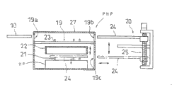
参照图8A和8B。图8A是一个具有临时基板堆放的加热舱PHP的侧视剖面图。图8B是其的侧视图。加热舱PHP包括用于加热放置上面的晶圆W的加热平台HP,用于将晶圆W保持在远离加热平台HP的上部位置或下部位置(在本实施例中是上部位置)的临时基板堆放19,以及用于在加热平台19和临时基板堆放19之间传送晶圆W的局部传送机构20。加热平台HP具有多个可凸出与平台上表面和收缩到平台上表面下面的支撑脚21。在加热平台HP上设置了上部盖子22,它可以在加热处理的时间中垂直移动来罩住晶圆W。临时基板堆放19具有多个固定的支撑脚23,用于支撑着晶圆W。See Figures 8A and 8B. Figure 8A is a side sectional view of a heating chamber PHP with temporary substrate stacking. Fig. 8B is a side view thereof. The heating chamber PHP includes a heating platform HP for heating a wafer W placed thereon, a temporary substrate stack for holding the wafer W in an upper position or a lower position (in this embodiment an upper position) away from the
局部传送机构20包括保持平台24,它用于以水平的姿态来保持晶圆W。保持平台24可以通过螺杆控制机构25来垂直移动,并且可以通过皮带传动机构26来延伸和收缩。保持平台24确定了多个切口,以避免在保持平台24超过加热平台HP或临时基板堆放19延伸时产生对可移动支撑脚21或固定支撑脚23的影响。局部传送机构20包括用于在晶圆W从加热平台HP到临时基板堆放19的传送过程中冷却晶圆W的装置。该冷却装置,例如,具有制成在保持平台24内用于循环冷却水的冷却水管道24b。The
局部传送机构20面对着在加热平台HP和临时基板堆放19范围内的第二主传送机构10B。即,将局部传送机构20设置在相邻于装置的背后表面上。加热平台HP和临时基板堆放19装入外壳27。外壳27具有一个制成在罩住临时基板堆放19的上部部分前壁上的开孔19a,以允许第二主传送机构10B能够进入;以及一个制成在上部部分后壁上的开孔19b,以允许局部主传送机构20能够进入。此外,外壳27还具有在罩住加热平台HP的下部部分的封闭前表面,和一个制成在下部部分后壁上的开孔19c,以局部主传送机构20能够进入。The
晶圆W将采用下列方式装入上述加热舱HPH和从加热舱HPH卸下。首先,主传送机构10(在光刻薄膜形成块3情况中的第二主传送机构10B)将晶圆W放置在临时基板堆放19的固定支撑脚23上。随后,局部传送机构20的保持平台接近晶圆W的下面并慢慢地从固定支撑脚23上抬起和拾取晶圆W。保持平台24保持着晶圆W放置到外壳27,并且到加热平台HP对面的位置放下晶圆W。这时,加热平台HP的可移动的支撑脚21处于较低的位置,并且提升上部盖子22。保持晶圆W的保持平台24接近于加热平台HP的上方。可移动的支撑脚21上升并拾取晶圆W,此后,保持平台24就离开外壳27。接着。可移动支撑脚21降低,使得晶圆W放置在加热平台HP上。上部盖子22降低,以罩住晶圆W。晶圆W以这种状态加热。在加热处理之后,提升上部盖子22。上升可移动的支撑脚21去拾取晶圆W。保持平台接近晶圆W的下面,随后可移动支撑脚23降低,使得晶圆W放置在保持平台24上。保持平台24保持着晶圆W离开外壳27,向上移动并将晶圆W传送到临时基板堆放19。在这个传送过程中,由保持平台24所支撑着的晶圆W被加热平台24的冷却功能所冷却。保持平台24将冷却后(即,返回到室温)的晶圆W传送到临时基板堆放19。主传送机构10取出和传送晶圆W。The wafer W will be loaded into and unloaded from the above-mentioned heating chamber HPH in the following manner. First, the main transfer mechanism 10 (second
正如以上所讨论的,主传送机构10只在临时基板堆放19中来回传送晶圆W,而不在加热平台HP中来回传送晶圆W。于是,主传送机构不会存在温度的增加。另外,用于向/从加热平台HP装入和卸下晶圆W的开孔19c位于远离主传送机构的一边。因此,主传送机构10不会被通过开孔19c所散发出来的热空气所加热。光刻薄膜涂覆舱15也就永远不会受到开孔19c所散发出来热空气的负面影响。As discussed above, the
显影块4设置于相邻上述讨论的光刻薄膜形成块3。正如图5所示,也在光刻薄膜形成块3和显影块4之间形成了一个大气屏蔽隔板13。该隔板13具有垂直排列的两个基板台PASS5和PASS6,用于在两个块3和4之间传送晶圆W;以及两个水冷却冷却平台WCP,以普通或广泛采用的方式来冷却晶圆W。The developing
下文将讨论显影块4。显影块4是一个用于显影已曝光的晶圆W的机构。具体地说,显影块4包括用于显影已曝光的晶圆W的显影舱30,用于热处理与显影有关的晶圆W的热处理舱,以及用于在显影舱30和热处理舱31之间来回传送晶圆W的第三主传送机构10C。The
正如图3所示,显影舱30包括五个显影舱30a-30e(下文在未指定各个显影舱的情况下称之为“30”),这五个显影舱30a-30e是垂直排列的相同结构。各个显影舱30包括了旋转卡盘32,用于吸住支撑和以水平姿态旋转晶圆W,和喷头33,其用于向旋转卡盘32所保持的晶圆W提供显影液。As shown in FIG. 3, the developing
正如图4所示,热处理舱31包括多个加热平台HP,多个具有临时基板堆放的加热舱HPH,以及多个冷却平台CP。如同在其它块2和3一样,这些热处理舱都是垂直排列的并分成多个塔。热处理舱31的右边一塔(相邻接口块5)包括基板台PASS7和PASS8,它们是以一个重叠于另一个并相互接近的方式排列,用于能使晶圆W传送于接口块5。上部基板台PASS7用于送入晶圆W,而下部基板台PASS8则用于返回晶圆W。As shown in FIG. 4 , the
接着讨论接口块5。接口块5是一个能使晶圆W在曝光装置STP来回传送的机构,它是与基板处理装置相分离的外部装置。在本实施例中的该接口块5,除了用于使晶圆W能在曝光装置STP之间传送的接口传送机构35之外,还包括两个用于对采用光刻胶涂覆晶圆W的边缘进行曝光的边缘曝光舱EEW,以及第四主传送机构10D,它用于在边缘曝光舱EEW和设置在显影块中的具有临时基板堆放的热处理舱PHP之间来回传送晶圆W。The
正如图3所示,每一个边缘曝光舱EEW都包括了旋转卡盘36,用于吸住支撑和以水平姿态旋转晶圆W,和发光器37,用于对旋转卡盘36所保持的晶圆W的边缘进行曝光。两个边缘曝光舱EEW以一个重叠另一个的方式排列在接口块5的中心位置上。设置在边缘曝光舱EEW的第四主传送机构10D和显影块4的热处理舱具有于图7A和7B所说明的主传送机构10的相同结构。As shown in FIG. 3 , each edge exposure cabin EEW includes a
参照图3和图6。图6是接口块5的侧视图。在两个边缘曝光舱EEW的下面设置了基板返回缓冲器RBF,以及在缓冲器RBF下面以一个重叠于另一个地排列着两个基板台PASS9和PASS10。基板返回缓冲器RBF提供临时存储显影块4热处理舱PHP正在进行后期曝光热处理的晶圆W,它适用于诸如由于某些故障显影块4不能显影晶圆W的时候。该缓冲RBF是以多级存储架的形式来存储多个晶圆W。基板台PASS9和PASS10用于在第四主传送机构10D和接口传送机构35之间传送晶圆W。上部的台是用于送入晶圆W,而下部的台则是用于返回晶圆W。Refer to FIG. 3 and FIG. 6 . FIG. 6 is a side view of the
正如图2和图6所示,接口传送机构35具有一个适用于Y方向水平移动的可移动基座35a;以及安装在可移动基座35a上用于保持晶圆W的保持臂35b。保持臂35b可以垂直移动,摇摆,以及可以摇摆移动的径向延伸和收缩。接口传送机构35具有它的传送路径的一端(图6所示的位置P1)可延伸到垂直排列的基板台PASS9和PASS10的下面。在位置P1,接口传送机构35将晶圆W传送进和传送出曝光装置STP。在传送路径的另一个端位置P2,接口传送机构35将晶圆W传送进和传送出PASS9和PASS10,以及将晶圆W堆放和送入/出到送入缓冲器SBF。当曝光装置STP不能再接受晶圆时,送入缓冲器SBF提供了待曝光晶圆W的临时存储,以及以多级存储架的形式来存储多个晶圆W。As shown in FIG. 2 and FIG. 6 , the
具有上述结构的基板处理装置将清洁空气的下游送入到分拣块1,各个处理舱2、3、和4,以及接口块5,以避免再这些块中所产生浮动的颗粒和气流对处理产生负面的影响。各个块的内部都维持着比装置的外部环境稍微高一些的压力,以避免颗粒、污染物等类似的东西从外部环境进入。特别是,抗反射薄膜形成块2设置了比分拣块更高的大气压力。由于分拣块1的气体不能流入反射薄膜形成块2,所以可以在没有外部气体的影响下,在各个块2,3和4中进行处理过程。The substrate processing apparatus having the above-mentioned structure feeds clean air downstream into the
接着将讨论基板处理装置的控制系统,特别是基板传送的控制。Next, the control system of the substrate processing apparatus, especially the control of substrate transfer will be discussed.
上述所讨论的分拣块1,抗反射薄膜形成块2,光刻薄膜形成块3,显影块4和接口块5都是形成基板处理装置的各个机构部分的部件。特别是,通过将各个块组装成各个块架构并将这些块架构连接成一体来形成基板处理装置(见图9A)。The above-discussed
另一方面,作为本发明的一个性能,所提供的有关基板处理装置的控制单元是与构成机构部件的块相分离的。即,每个单个的控制单元包括了对基板进行所需处理的处理舱,以及单个用于将基板传送进出处理舱的主传送机构。这类控制单元是以并行的方式构成了基板处理装置。各个控制单元的主传送机构通过基板台来传送基板,并且每个控制单元包括一个控制器件,它用于每个控制单元主传送机构的至少基板传送操作。每控制单元的控制器件都独立于其它控制器件,进行一系列有关基板传送的控制,这些控制包括将基板来回传送于处理舱以将基板来回传送于基板台的传送控制。On the other hand, as one feature of the present invention, there is provided a control unit related to a substrate processing apparatus separated from the blocks constituting the mechanism parts. That is, each individual control unit includes a processing chamber for performing the desired processing on the substrates, and a single main transfer mechanism for transferring the substrates into and out of the processing chambers. Such control units constitute a substrate processing apparatus in parallel. The main transport mechanism of each control unit transports the substrate through the substrate stage, and each control unit includes a control device for at least the substrate transport operation of the main transport mechanism of each control unit. The control device of each control unit is independent of other control devices, and performs a series of control related to substrate transfer, and these controls include the transfer control of transferring the substrate to and from the processing chamber and transferring the substrate to and from the substrate table.
在本实施例中的控制单元下文称之为“单元”。图9B显示了本实施例的单元结构。The control unit in this embodiment is hereinafter referred to as "unit". Fig. 9B shows the cell structure of this embodiment.
分拣单元C1包括了盒子架6和分拣传送机构7。此外,该单元C1具有相同于机械性划分部件的分拣块1的结构。抗反射薄膜形成单元C2包括抗反射薄膜涂覆舱8,抗反射薄膜热处理舱9和第一主传送机构10A。此外,该单元C2也具有相同于机械性划分部件的抗反射薄膜形成块2的结构。光刻薄膜形成单元C3包括光刻薄膜涂覆舱15,光刻薄膜热处理舱16和第二主传送机构10B。此外,该单元C3也具有相同于机械性划分部件的光刻薄膜形成块3的结构。The sorting unit C1 includes a
另一方面,显影单元C4包括显影舱30,除了用于后期曝光加热的热处理舱(本实施例中的加热舱PHP)之外的热处理舱31,以及第三主传送机构10C。该单元C4具有不同于机械性划分部件的显影块4的结构,除了用于后期曝光加热的热处理舱PHP之外。On the other hand, the developing unit C4 includes a developing
后期曝光加热C5包括用于在显影之前加热曝光过的晶圆W的后期曝光加热舱(即,在该实施例中,安排在显影块4中的加热舱PHP),边缘曝光舱EEW以及第四主传送机构10D。该单元C5显影块4和构成了机械性划分部件的接口块5的桥梁,并且具有本实施例特征的单元。由于后期曝光处理舱(即,加热舱PHP)和第四主传送机构10D是合并成一个单独的单元,正如以上所提到,曝光后的晶圆W可以迅速地装入到加热舱PHP中,进行热处理。这在使用在曝光后需要迅速加热的化学增强光刻胶的情况中是非常有利的。The post-exposure heating C5 includes a post-exposure heating chamber (ie, in this embodiment, a heating chamber PHP arranged in the developing block 4) for heating the exposed wafer W before development, an edge exposure chamber EEW, and a fourth
接口单元C6包括接口传送机构35,它用于将晶圆W传送进出外部装置的曝光装置STP。该单元C6并不包括第四主传送机构10D或边缘曝光舱EEW,以及,在这方面,不同于机械性划分部件的接口块5。The interface unit C6 includes an
该实施例具有上述以并行方式排列的六个单元C1-C6。晶圆W通过基板台PASS1-PASS10在单元C1-C6之间传送。换句话说,本发明的每一个控制单元(单元)都包括单独的主传送机构和处理舱,主传送机构在将晶圆W放置在其它基板台上以前从一个指定基板台接受晶圆W将其传送进出处理舱。This embodiment has the aforementioned six cells C1-C6 arranged in parallel. Wafers W are transferred between cells C1-C6 via substrate stages PASS1-PASS10. In other words, each control unit (unit) of the present invention includes a separate main transfer mechanism and a processing chamber, and the main transfer mechanism receives a wafer W from a designated substrate stage before placing the wafer W on other substrate stages. It is transported into and out of the processing chamber.
单元C1-C6分别包括控制器CT1-CT6,分别用于至少控制主传送机构(包括分拣传送机构7和接口传送机构35)的基板传送操作。各个控制器CT1-CT6单独进行一系列控制,从预定基板台接受到晶圆W开始,以及将晶圆W放置在预定基板台结束。特别是,正如图10A所示,各个单元C1-C6的控制器CT1-CT6采用一个控制器向已经将晶圆W放置在预定基板台的下一个单元的控制器发送信息的方式来交换信息,并且已经接受到晶圆W的下一个单元的控制器向从预定基板台上接受到晶圆W的前述单元的控制器返回信息。The units C1-C6 respectively include controllers CT1-CT6 for controlling at least the substrate transfer operation of the main transfer mechanism (including the sorting
也就是说,每一个控制器CT1-CT6都只对在它单元中的晶圆W的传送进行控制,而与相邻单元的主传送机构的移动无关。于是,控制器CT1-CT6在减小的控制负载下操作。在常规基板处理装置的控制方法中,正如图10B所示,每一个块1-5都向控制器CTO发送有关基板传送的信息,以便于时间管理,以及控制器CTO进行基板传送的整体控制。于是,控制器CTO具有增加的负载。That is to say, each controller CT1-CT6 only controls the transfer of the wafer W in its unit, regardless of the movement of the main transfer mechanism of the adjacent unit. Thus, the controllers CT1-CT6 operate under reduced control load. In the control method of a conventional substrate processing apparatus, as shown in FIG. 10B, each block 1-5 sends information about substrate transfer to the controller CTO for time management, and the controller CTO performs overall control of substrate transfer. Then, the controller CTO has an increased load.
在该实施例中,控制器CT1-CT6是在减小负载的条件下操作的,正如以上所讨论的,因此,相应地基板处理装置提高了产量。在如图10B所示的常规控制方法中,处理舱新近增加了所需的部分,该部分是在控制器CTO中的时间管理程序的扩展版本。在根据本发明的控制方法中,一个单元可以容易地增加,因为它不会对相邻单元产生任何影响。所增加的单元并不限制于特殊的类型。例如,检查单元可以增加在光刻薄膜形成单元C3和显影单元C4之间,用于检查在晶圆W上所制成的光刻薄膜的厚度或用于检查显影的光刻薄膜的线宽。在这种情况下,检查单元,正如本实施例的其它单元所做的那样,包括用于检查基板的基板检查舱,和用于使基板能进出检查舱的主传送机构。基板通过基板台在检查单元和相邻单元之间传送。In this embodiment, the controllers CT1-CT6 are operated under reduced load conditions, as discussed above, and accordingly, the throughput of the substrate processing apparatus is increased accordingly. In the conventional control method as shown in Fig. 10B, the process bay newly adds the required part, which is an extended version of the time management program in the controller CTO. In the control method according to the present invention, a unit can be added easily because it does not have any influence on the adjacent units. The added units are not limited to a particular type. For example, an inspection unit may be added between the photoresist film forming unit C3 and the developing unit C4 for inspecting the thickness of the photoresist film formed on the wafer W or for inspecting the line width of the developed photoresist film. In this case, the inspection unit, like the other units of this embodiment, includes a substrate inspection chamber for inspecting substrates, and a main transport mechanism for enabling substrates to enter and exit the inspection chamber. Substrates are transferred between the inspection unit and adjacent units by the substrate stage.
在主传送机构从指定位置向另一个位置传送晶圆W的情况下,作为一个步骤,在各个抗反射薄膜形成单元C2,光刻薄膜形成单元C3和显影单元C4中,具有对不同的化学处理的不同控制单元,在单元C2、C3和C4中的第一、第二和第三主传送机构10A、10B和10C基本上进行相同数量的传送步骤。这是在本实施例中的基板处理装置的另一性能。而它的细节将从下文所讨论的本实施例装置的操作中明白,正如图11所示,每一个上述主传送机构10A、10B和10C进行大约六个传送步骤。In the case where the main transport mechanism transports the wafer W from a designated position to another position, as a step, in each of the antireflection film forming unit C2, photolithographic film forming unit C3, and developing unit C4, there is a process for different chemical treatments. The different control units, the first, second and third
在本实施例中,主传送机构10大约4秒中完成一个传送步骤。于是,采用主传送机构10进行六个传送步骤,每一个单元C2-C3每24秒将一个晶圆W传递给相邻的单元(即,在24秒的处理周期中)。也就是说,该装置能够每小时处理150个晶圆W。如果一个主传送机构进行了比其它主传送机构更多的传送步骤,则基板处理装置的产量取决于一个主传送机构所述单元的处理周期。例如,在单元C2和C4中的各主传送机构10A和10C进行五个传送步骤,和单元C3的主传送机构10B进行了八个传送步骤,晶圆W只在单元C3的处理周期中流动在单元C2-C4之间(在该情况下,这是32秒)。即使单元C2和C4中的各主传送机构10A和10C能够提供传送多个晶圆W,基板处理装置能够在每小时中只处理112.5个晶圆。In this embodiment, the main conveying
在本实施例中,另一方面,抗反射薄膜形成单元C2,光刻薄膜形成单元C3和显影单元C4的每个主传送机构10A,10B和10C都共享基本相同数量的传送步骤。该实施例避免了一个主传送机构比其它主传送机构更早地达到传送处理限度的状态。因此,基板处理装置提供了提高的产量。In this embodiment, on the other hand, each of the
有关设置于相邻显影单元C4的曝光后加热单元C5,将该单元C5的第四主传送机构10D设置成进行第五传送步骤。曝光后加热单元C5要求对从曝光到晶圆W加热的时间进行严格管理。于是,从容许自由度的观点触发,第四主传送机构10D给出了比其它主传送机构更轻的传送负载。在对第四主传送机构10D不需要这类自由度的情况下,该加热单元C5必须有一个传送步骤的余量。该传送的余量可以用于对曝光后加热单元C5增加一个新的处理舱,例如,用于检查晶圆W的舱。即使增加这类基板检查舱,单元C5的主传送机构10D只共享与其它单元的主传送机构同样做的六个传送步骤。也就是说,即使在对具有传送余量的单元C5增加基板检查舱的情况下,单元C5具有与其它单元相同的24秒的处理周期。这就不会减少基板处理装置的产量。Regarding the post-exposure heating unit C5 provided adjacent to the developing unit C4, the fourth
接着讨论本实施例中基板处理装置的操作。见图11,由抗反射薄膜形成单元C2,光刻薄膜形成单元C3,显影单元C4和曝光后加热单元C5的主传送机构10A-10D所进行的传送步骤。Next, the operation of the substrate processing apparatus in this embodiment will be discussed. See FIG. 11, the transfer steps performed by the
首先,分拣单元C1(分拣块1)的分拣传送机构7水平移动到预定盒子C的对面位置。随后,将待处理的晶圆W通过提高垂直移动和延伸和收缩保持臂7b从盒子C取回。采用保持臂7b来保持晶圆W,分拣传送机构7水平移动到相对于基板台PASS1和PASS2的位置。随后,传送机构7将保持臂所保持的晶圆W放置在上部基板送入台PASS1的上面。当在下部基板返回台PASS2上发现处理后的晶圆W时,分拣传送机构7将处理后的晶圆W装上保持臂7b,并且将该处理后的晶圆W堆放在预定的盒子C中。此外,传送机构7重复从盒子C中取出待处理晶圆W,将晶圆W传送到基板台PASS1,从基板台PASS2接受处理后的晶圆W,以及将处理后的晶圆W堆放与盒子C中的操作。First, the sorting
将讨论抗反射薄膜形成单元C2(抗反射薄膜形成块2)的操作。在将待处理晶圆W放置于基板台PASS1之后,正如图11所示,单元C2的第一主传送机构10A垂直移动并且与保持臂10a和10b一起摇摆,使之移到相对于基板台PASS1和PASS2的位置上。第一主传送机构10A进行将由一个保持臂10b保持的晶圆W放置于下部基板返回台PASS2,以及随后将基板送入台PASS1上的待处理晶圆装上另一个保持臂10a的晶圆传送操作。特别是,保持臂10b先将处理后的晶圆W放置于基板台PASS2。释放处理晶圆W的保持臂10b限制在原始位置上。随后,保持臂10a和10b一起稍微提升些,此后保持臂10a先从基板台PASS1上拾取待处理晶圆W。已经接受了晶圆W保持臂10a缩回到原始的位置上。The operation of the antireflection film forming unit C2 (antireflection film forming block 2) will be discussed. After placing the wafer W to be processed on the substrate stage PASS1, as shown in FIG. And the position of PASS2. The first
待处理晶圆W和处理后晶圆W在基板台PASS1和PASS2之间的上述来回传送可以由图11的第一主传送机构10A的传送步骤(1+α)来表示。这里,“α”表示将保持臂10a和10b从相对于基板台PASS2的位置稍微提升到相对于基板台PASS1的位置的部分传送步骤,以便于从基板台PASS1上接受待处理的晶圆W。正如以上所提到的那样,基板台PASS1和PASS2是垂直排列的且相互接近的。在基板台PASS1和PASS2之间移动所消耗的时间是很短的且可以忽略不计。于是,传送步骤(1+α)可以被认为是一个传送步骤(即,在本实施例中,是在预定的时间(例如,4秒钟)内由主传送机构所完成的基板传送操作)。The above-mentioned back-and-forth transfer of the wafer W to be processed and the processed wafer W between the substrate stages PASS1 and PASS2 can be represented by the transfer step (1+α) of the first
一旦完成了晶圆W在基板台PASS1和PASS2之间的传送之后,第一主传送机构垂直移动并且与保持着待处理晶圆W的保持臂10a一起摇摆,以及将没有保持晶圆W的未装载保持臂10b移至相对于抗反射薄膜热处理舱9的预定冷却平台CP的位置上。通常,将先前处理过的晶圆W放置于该冷却平台CP。于是,未装载保持臂10b就首先从冷却平台CP上拾取冷却后的晶圆W。随后,保持待处理晶圆W的保持臂10a先将待处理晶圆W放置于冷却平台CP上。放置于冷却平台CP上的晶圆W以较高的精度冷却到室温,同时主传送机构10A进行其它的传送操作。可以在没有垂直移动两个保持臂10a和10b的条件下进行冷却平台CP的晶圆W的来回传送操作。于是,可以在第一主传送机构10A的一个传送步骤中完成冷却平台CP晶圆W的来回传送操作(见图11所示第一主传送机构10A哦传送步骤(2))。Once the transfer of the wafer W between the substrate stages PASS1 and PASS2 is completed, the first main transfer mechanism moves vertically and swings together with the holding
一旦完成了将晶圆W进出冷却平台CP的传送操作,第一主传送机构就垂直移动并且与未装载的保持臂10a一起摇摆,以及使保持着冷却后晶圆W的保持臂10b移至相对于一个预定抗反射薄膜涂覆舱8的位置上。通常,在抗反射薄膜涂覆舱8中有着先前处理过的晶圆W。于是,未装载保持臂10a就首先从抗反射薄膜涂覆舱8的旋转卡盘11上拾取处理后的晶圆W。然后持有晶圆W的保持臂10b前进将晶圆W放置到卡盘11上。放置在旋转卡盘11上的晶圆W采用抗反射薄膜涂覆,同时主传送机构10A进行其它传送操作。晶圆W对旋转卡盘11的传送对应着图11所示的第一主传送机构10A的传送步骤(3)。在图11中的“BARC”表示抗反射薄膜涂覆舱8。Once the transfer operation of the wafer W into and out of the cooling platform CP is completed, the first main transfer mechanism moves vertically and swings together with the unloaded holding
一旦完成了晶圆W对旋转卡盘11的传送,第一主传送机构10A就垂直移动并且与保持着涂覆了抗反射薄膜的晶圆W的保持臂10a一起摇摆,以及使没有保持晶圆W的保持臂10b移至相对于预定加热平台HP的位置上。通常,在加热平台HP上也有着先前处理过的晶圆W。于是,未装载的保持臂10b就先从加热平台HP上拾取加热的晶圆W。随后,保持臂10a就将待处理的晶圆W放置于加热平台HP上。放置于加入平台HP上的晶圆W加热处理,使得具有多余的溶剂从晶圆W的抗反射薄膜上消除,同时,主传送机构10A进行其它传送操作。晶圆W对加热平台HP的来回传送操作对应着图11所示的第一主传送机构的传送步骤(4)。Once the transfer of the wafer W to the
一旦晶圆W对加热平台HP的传送操作完成之后,第一主传送机构10A就垂直移动并且与未装载的保持臂10a一起摇摆,以及将保持着加热晶圆W的保持臂10b移至相对一个安装在隔板13中的水冷冷却平台WCP的位置上。正如在上述提及的情况那样,未装载保持臂10a首先从冷却平台WCP上拾取处理后的晶圆W。随后,保持臂10b先将晶圆W放置于冷却平台WCP上。放置在冷却平台WCP上的晶圆W很快就冷却了,同时主传送机构10A进行其它传送操作。晶圆W对冷却平台WCP的来回传送操作对应着图11所示的第一主传送机构10A的传送步骤(5)。Once the transfer operation of the wafer W to the heating platform HP is completed, the first
一旦晶圆W完成了对冷却平台WCP的传送操作之后,第一主传送机构10A就与保持着大致冷却了的晶圆W的保持臂10a和未装载保持臂10b一起提升移至相对于冷却平台WCP上述排列的基板台PASS3和PASS4的位置上。保持臂10a先将晶圆W放置于上部的基板送入台PASS3上。通常,下部基板返回台PASS4保持着显影过的晶圆W,它使从显影单元C4通过光刻薄膜形成单元C3传送过来的。在稍微降低了保持臂10a和10b之后,保持臂10b就先从基板台PASS4上拾取显影后的晶圆W。Once the wafer W has completed the transfer operation to the cooling platform WCP, the first
晶圆W对基板台PASS3和PASS4的传送操作对应着图11所示的第一主窜送机构10A的传送步骤(6+α)。正如以上所提及的那样,“α”只是表示稍微提升和降低保持臂10a和10b的传送步骤的短暂部分。于是,传送步骤(6+α)可以被认为是一个传送步骤。The transfer operation of the wafer W to the substrate stages PASS3 and PASS4 corresponds to the transfer step (6+α) of the first
抗反射薄膜形成单元C2的第一主传送机构10A重复上述所讨论的传送步骤(1+α)至传送步骤(6+α)。传送步骤(1+α)至传送步骤(6+α)的总的步骤大约为第一主传送机构10A的六个传送步骤。假定一个传送步骤需要4秒钟,则第一主传送机构10A可在24秒钟内完成基板传送的一个周期。换句话说,抗反射薄膜形成单元C2每24秒钟将向下一个光刻薄膜形成单元C3送入一个晶圆W(即,每小时150个晶圆W)。The first
将讨论光刻薄膜形成单元C3(光刻薄膜形成块3)的操作。在将具有反射薄膜涂覆的晶圆W放置于基板台PASS3之后,正如图11所示,单元C3的第二主传送机构10B利用一个保持臂10b将显影后的晶圆W放置在基板台PASS4上。随后,第二主传送机构10B就将基板台PASS3上的晶圆W装载上保持臂10a。由图11中的第二主传送机构10B的传送步骤(1+α)来表示晶圆W对基板台PASS3和PASS4的传送操作。正如以上所提及的那样,“α”表示了一个可以忽略的时间,并且传送步骤(1+α)可视为一个传送步骤。The operation of the photoresist film forming unit C3 (photoresist film forming block 3) will be discussed. After placing the wafer W coated with a reflective film on the substrate stage PASS3, as shown in FIG. superior. Subsequently, the second
一旦完成了晶圆W等对基板台PASS3和PASS4的传送操作之后,第二主传送机构10B就将保持着晶圆W的保持臂10a和没有保持晶圆W的保持臂10b移动至相对于光刻薄膜热处理舱16的预定冷却平台CP的位置上。未装载的保持臂10b就首先从冷却平台CP上拾取冷却的晶圆W。随后,保持臂10a先将待冷却的晶圆W放置于冷却平台CP上。晶圆W对冷却平台CP的传送操作对应着图11所示的第二主传送机构10B的传送步骤(2).Once the transfer operation of the wafer W and the like to the substrate stages PASS3 and PASS4 is completed, the second
一旦完成了晶圆W对冷却平台CP的传送操作之后,第二主传送机构10B就将未装载保持臂10a和保持着冷却晶圆W的保持臂10b移动至相对于预定的一个光刻薄膜涂覆舱15的位置上。未装载保持臂10a首先从光刻表面涂覆舱15的旋转卡盘17上拾取处理后的晶圆W。随后,保持晶圆W的保持臂10b先将晶圆W放置在旋转卡盘17上。放置在旋转卡盘17上的晶圆W采用光刻胶薄膜涂覆,同时主传送机构10B进行其它传送操作。晶圆W对旋转卡盘17的传送操作对应着图11所示的第二主传送机构的传送步骤(3)。在图11中的“PR”表示光刻薄膜涂覆舱8。Once the transfer operation of the wafer W to the cooling platform CP is completed, the second
一旦完成晶圆W对旋转卡盘17的传送操作之后,第二主传送机构10B就将保持具有光刻薄膜涂覆晶圆W的保持臂10a和没有保持晶圆W的保持臂10b移动至相对于具有临时基板堆放19的预定加热舱PHP的位置上,未装载保持臂10b首先从加热舱PHP的临时基板堆放19拾取处理后的晶圆W。随后,保持臂10a将待处理的晶圆W放置于临时基板堆放19。在主传送机构10B进行其它传送操作的同时,局部传送机构20将放置于临时基板堆放19的晶圆W传送到用于加热处理的加热舱PHP的加热平台HP上。通过相同的局部传送机构20可将加热平台HP上的加热处理晶圆W返回到临时基板堆放19。在返回到临时基板堆放19的同时,正如由局部传送机构20的保持平台24所保持的那样,晶圆W由保持平台24的冷却机构来冷却。晶圆W对加热藏PHP的传送操作对应着图11所示的第二主传送机构10B的传送步骤(4)。Once the transfer operation of the wafer W to the
一旦完成了晶圆W对加热舱PHP的传送操作之后,第二主传送机构10B将未装载保持臂10a和保持着加热晶圆W的保持臂10b移动至相对于光刻薄膜热处理舱16的冷却平台CP的位置上。未装载保持臂10a首先从冷却平台CP拾取冷却的晶圆W。随后,保持臂10b将待处理的晶圆W放置在冷却平台CP上。晶圆W对冷却平台CP的传送对应着图11所示的第二主传送机构的传送步骤(5)。Once the transfer operation of the wafer W to the heating chamber PHP is completed, the second
一旦完成了晶圆W对冷却平台CP的传送操作之后,第二主传送机构10B将保持着冷却的晶圆W的保持臂10a和未装载保持臂10b移动至相对于基板台PASS5和PASS6的位置上。保持臂10a首先将晶圆W放置于上部基板送入台PASS5上,并且保持臂10b从下部基板返回台PASS6拾取显影后的晶圆W。Once the transfer operation of the wafer W to the cooling platform CP is completed, the second
晶圆W对基板台PASS5和PASS6的传送操作对应着图11所示的第二主传送机构10B的传送步骤(6+α)。传送步骤(6+α)被视为一个传送步骤。The transfer operation of the wafer W to the substrate stages PASS5 and PASS6 corresponds to the transfer step (6+α) of the second
光刻薄膜形成单元C3的第二主传送机构10B重复上述讨论的传送步骤(1+α)至传送步骤(6+α)。总的传送步骤(1+α)至传送步骤(6+α)产生大约六个第二主传送机构10B的传送步骤,如同第一主传送机构10A的情况。于是,第二主传送机构10B所完成一个基板传送周期相同于第一传送机构10A所完成的相同一个基板传送周期(在本实施例中,大约每24秒钟内完成一个周期)。换句话说,光刻表面形成单元C3每24秒(即,每小时150个晶圆W)向下一个显影单元C4送入一个晶圆W。The second
将讨论显影单元C4的操作。在光刻薄膜涂覆的晶圆W放置于基板台PASS5之后,正如图11所示,单元C4的第三主传送机构10C将一个保持臂10b所保持着的显影后晶圆W放置于基板台PASS6上。随后,第三主传送机构10C将来自基板台PASS5的晶圆W装载上保持臂10a。晶圆W对基板讨PASS5和PASS6的传送操作可以由图11中的第三主传送机构10C的传送步骤(1+α)来表示。The operation of the developing unit C4 will be discussed. After the wafer W coated with the photolithographic film is placed on the substrate stage PASS5, as shown in FIG. On PASS6. Subsequently, the third
一旦完成的晶圆W对基板台PASS5和PASS6的传送操作以后,第三传送机构10C就将保持着晶圆W的保持臂10a和没有保持晶圆W的保持臂10b一起移动至降低于基板台PASS7和PASS8的位置上,这些位置都包括在加热处理舱31的垂直结构中。保持臂10a首先将涂覆了光刻薄膜的晶圆W放置于上部基板送入台PASS7上。随后,保持臂10b从下部基板返回台PASS8上拾取正在进行曝光后加热处理的晶圆W。晶圆W对基板台PASS7和PASS8的传送操作可由图11所示的第三主传送机构10C的传送步骤(2+α)来表示。Once the transfer operation of the wafer W to the substrate stages PASS5 and PASS6 is completed, the
一旦完成了晶圆W对对基板台PASS7和PASS8的传送操作之后,第三主传送机构10C就将未装载的保持臂10a和保持着曝光和热处理后的晶圆W的保持臂10b移动至相对于热处理舱31的预定冷却平台CP的位置上。未装载的保持臂10a首先从冷却平台CP拾取冷却后的晶圆W。随后,保持臂10b将待处理的晶圆W放置于冷却平台CP上。晶圆W对冷却平台CP的传送操作对应着图11所示的第三主传送机构10C的传送步骤(3)。Once the transfer operation of the wafer W pair to the substrate stages PASS7 and PASS8 is completed, the third
一旦完成了晶圆W对冷却平台CP的传送操作之后,第三主传送机构10C就将保持着冷却晶圆W的保持臂10a和未装载的保持臂10b移动至显影舱30的预定位置上。未装载的保持臂10b首先从显影舱的旋转卡盘32上拾取处理后的晶圆W。随后,保持着晶圆W保持臂10a将晶圆W放置于旋转卡盘32上。放置于旋转卡盘32的晶圆W进行显影,同时主传送机构10C进行其它传送的操作。晶圆W对旋转卡盘32的传送操作对应着图11所示的第三主传送机构10C的传送步骤(4)。图11中的“SD”表示显影舱8。Once the transfer operation of the wafer W to the cooling platform CP is completed, the third
一旦完成了晶圆W对旋转卡盘32的传送操作之后,第三主传送机构10C就将未装载的保持臂10a和保持着显影后的晶圆W的保持臂10b移动至相对于显影舱31预定加热平台HP的位置上。未装载的保持臂10a首先从加热平台HP上拾取处理后的晶圆W。随后保持臂10b将待处理的晶圆W放置于加热平台HP。晶圆W对加热平台HP的传送操作对应着图11所示的第三主传送机构10C的传送步骤(5)。Once the transfer operation of the wafer W to the
一旦完成了晶圆W对加热平台HP的传送操作之后,第三主传送机构10C就将保持着加热处理的晶圆W的保持臂10a和未装载的保持臂10b移动至相对于安装在邻近光刻薄膜形成单元C3隔板13中的水冷冷却平台WCP的位置上。未装载的保持臂10b首先从水冷冷却平台WCP上拾取处理后的晶圆W,以及保持臂10a将待处理的晶圆W放置于冷却平台WCP上。晶圆W对冷却平台WCP的传送操作对应着图11所示的第三主传送机构10C的传送步骤(6)。Once the transfer operation of the wafer W to the heating platform HP is completed, the third
显影单元C4的第三主传送机构10C重复上述讨论的传送步骤(1+α)至传送步骤(6)。总的传送步骤(1+α)至传送步骤(6)产生大约六个第三主传送机构10C的传送步骤,如同第一和第二主传送机构10A和10B的情况。于是,第三主传送机构10C所完成一个基板传送周期相同于第一和第二传送机构10A和10B所完成的相同一个基板传送周期(在本实施例中,大约每24秒钟内完成一个周期)。换句话说,显影单元C4每24秒向下一个曝光后加热单元C5送入一个晶圆W(即,每小时150个晶圆W)。The third
讨论曝光后加热单元C5的操作。在将具有光刻薄膜涂覆的晶圆W放置于基板台PASS7之后,正如图11所示,单元C5的第四主传送机构10D利用保持显影和加热后的晶圆W的保持臂10b将晶圆W放置于基板台PASS8上。随后,第四主传送机构10D将基板讨PASS7的晶圆W装入保持臂10a。晶圆W对基板台PASS7和PASS8的传送操作可由图11中的第四主传送机构10D的传送步骤(1+α)来表示。The operation of the post-exposure heating unit C5 is discussed. After placing the wafer W coated with a photolithographic film on the substrate stage PASS7, as shown in FIG. The circle W is placed on the substrate stage PASS8. Subsequently, the fourth
一旦完成了晶圆W对基板台PASS7和PASS8的传送操作之后,第四主传送机构10D就将保持着晶圆W的保持臂10a和未装载的保持臂10b移动至一个边缘曝光舱EEW的预定位置上。未装载的保持臂10b首先从边缘曝光舱EEW中的旋转卡盘36上拾取边缘曝光后的晶圆W。随后,保持着晶圆W的保持臂10a将晶圆W放置于旋转卡盘36上。放置于旋转卡盘36上的晶圆W进行边缘曝光,同时主传送机构10D进行其它传送的操作。晶圆W对旋转卡盘36的传送操作对应着图11所示的第四主传送机构10D的传送步骤(2)。Once the transfer operation of the wafer W to the substrate stages PASS7 and PASS8 is completed, the fourth
一旦完成了晶圆W对旋转卡盘36的传送操作之后,第四主传送机构10D就将未装载的保持臂10a和保持着边缘曝光的晶圆W的保持臂10b移动至相对于加热处理舱31的预定冷却平台CP的位置上。未装载的保持臂10a首先从冷却平台CP上拾取处理后的晶圆W,以及保持臂10b将边缘曝光的晶圆W放置于冷却平台CP上。晶圆W对冷却平台CP的传送操作对应于图11所示的第四主传送机构10D的传送步骤(3)。Once the transfer operation of the wafer W to the
一旦完成了晶圆W对冷却平台CP的传送操作之后,第四主传送机构10D就将保持着冷却晶圆W的保持臂10a和未装载的保持臂10b移动至相对于基板台PASS9和PASS 10的位置上。随后,保持臂10a首先将晶圆W放置于上部基板送入台PASS9,而保持臂10b则从下部返回台PASS10中拾取在曝光装置中曝光的晶圆W。晶圆W对基板台PASS9和PASS10的传送操作对应于图11所示的第四主传送机构10D的传送步骤(4+α)。Once the transfer operation of the wafer W to the cooling platform CP is completed, the fourth
一旦完成了晶圆W对基板台PASS9和PASS10的传送操作之后,第四组传送机构10D就将未装载的保持臂10a和保持着曝光的晶圆W的保持臂10b移动至相对于热处理舱31的具有临时基板堆放的预定加热舱PHP的位置上。未装载的保持臂10a首先从加热舱PHP(更具体地是从临时基板堆放19)中拾取曝光和加热后的晶圆W。随后,保持臂10b将曝光后的晶圆W放置于加热舱(更具体的是放置于临时基板堆放19)。在主传送机构10D进行其它传送操作的同时,局部传送机构20将临时基板堆放19所放置的晶圆W传送至加热平台HP,进行加热处理。紧接着,利用同一个局部传送机构20将加热的晶圆W返回到临时基板堆放19。晶圆W对加热舱PHP的传送操作对应于图11所示的第四主传送机构的传送步骤(5)。Once the transfer operation of the wafer W to the substrate stages PASS9 and PASS10 is completed, the fourth set of
曝光后的加热单元C5的第四主传送机构10D重复上述所讨论的传送步骤(1+α)至传送步骤(5)。总的传送步骤(1+α)至传送步骤(5)可大约产生第四传送机构10D的五个传送步骤,这比第一至第三主传送机构10A-10C所共享的传送步骤少一个步骤。仅仅是在曝光后的加热单元C5中,当一个传送步骤需要4秒钟时,第四主传送机构10D可在20秒的周期中操作的。然而,由于另一个方面,第一至第三主传送机构10A至10C时在24秒的周期中操作的,所以在此之后,曝光后加热单元C5,以类似其它单元的相同速率,每24秒向下一个接口单元C6送入一个晶圆W(即,每小时150个晶圆W)。The fourth
讨论接口单元C6的操作。在边缘曝光后的晶圆W放置于基板台PASS9之后,接口单元C6的传送机构35就从基板台PASS9接受晶圆W,并将晶圆W放置于相邻的曝光装置STP。此外,接口传送机构35接受来自曝光装置STP的曝光过的晶圆W,并且将该晶圆W放置于基板返回台PASS10。接口传送机构35重复该基板传送的操作。The operation of interface unit C6 is discussed. After the edge-exposed wafer W is placed on the substrate stage PASS9, the
在本实施例的基板处理装置中,正如上述所讨论的,各个单元C1-C6在控制器CT1-CT6的控制下,利用主传送机构10来传送晶圆W(然而,分拣单元C1采用分拣传送机构7,以及接口单元C6采用接口传送机构35)。两个相邻的单元交换基板传送的信息,这些信息仅仅表示晶圆已经放置于基板台PASS,以及已经接受到了晶圆。也就是说,各个单元至在它自身内部进行基板的传送并且是在没有监控基板在相邻单元之间的基板传送状态的条件下单独完成的。于是,单元并不需要在同一时间来释放晶圆W,并可以具有一定的时间延迟。然而,这种时间延迟是可以被晶圆W保持在提供用于相邻单元之间晶圆W传送基板台上的时间变化长度所吸收。基板在相邻单元之间传送的时间延迟永远不会影响基板的传送。In the substrate processing apparatus of this embodiment, as discussed above, each unit C1-C6 uses the
因此,根据本实施例,控制器CT1-CT6能够减小控制单元C1-C6的负载,从而基板处理装置能够相应提高产量,并且还可以具有相对较为简单的结构。基板检查单元包括基板检查舱,以及主传送机构可以容易地安装在适当的单元之间,这使得基板处理装置可具有较高的灵活性。此外,在装置包括比其它单元少的传送步骤的情况下(在本实施例中,曝光后的加热单元C5),可以在不影响其它单元的条件下容易地向该单元增加新的处理舱(例如,基板检查舱)。Therefore, according to the present embodiment, the controllers CT1-CT6 can reduce the load of the control units C1-C6, so that the substrate processing apparatus can increase the output accordingly, and can also have a relatively simple structure. The substrate inspection unit includes the substrate inspection cabin, and the main transfer mechanism can be easily installed between appropriate units, which allows the substrate processing apparatus to have high flexibility. Furthermore, in cases where the setup includes fewer transfer steps than other units (in this example, post-exposure heating unit C5), new process chambers can be easily added to this unit without affecting other units ( e.g. substrate inspection chamber).
曝光装置STP或显影单元C4由于某些故障会变得难以接受晶圆W。以下将讨论这类故障的操作。The exposure device STP or the developing unit C4 may become difficult to accept the wafer W due to some failure. Actions for such faults are discussed below.
假定曝光装置STP变得不能接受晶圆W。在这种情况下,接口单元C6的传送机构35从基板台PASS9上拾取晶圆W,并且临时存储这些晶圆W在送入缓冲器SBF中。只对存储在缓冲器SBF中的晶圆W的数量继续处理。当缓冲器SBF期望不再包含更多的晶圆W时,就停止从分拣单元C1送入晶圆W的操作。当曝光装置STP变得能接受晶圆W的准备状态时,接口传送机构35就以存储晶圆W的次序重新从缓冲器SBF中送入晶圆W,并将晶圆W送入到曝光装置STP。随后,装置又重新开始正常的操作。Assume that the exposure apparatus STP becomes unable to accept the wafer W. In this case, the
假定显影单元C4变得不能接受晶圆W。在这种情况下,接口传送机构35,就如同正常的一样,将来之曝光装置STP的陆续返回的晶圆W送入到基板台PASS10。曝光后加热单元C5的第四主传送机构10D如同正常的一样将曝光后的晶圆W送入到加热舱PHP中。第四主传送机构10D临时存储这正在加热舱PHP中进行曝光后加热处理的晶圆W,在单元C5中的基板返回缓冲器RBF中,取代了在基板台PASS8上的这些晶圆W。对已经装入曝光装置STP的晶圆W的数量进行类似曝光后的加热,并且这些晶圆W随后被存储于基板返回缓冲器RBF中。当显影单元C4变得准备接受晶圆W时,第四主传送机构10D以晶圆W存储的次序从缓冲器RBF取出晶圆W,并放置于基板台PASS8。随后,装置又开始重新使用正常的操作。Assume that the developing unit C4 becomes unable to accept the wafer W. In this case, the
在上述讨论的装置中,曝光后加热处理单元C5提供基板返回缓冲器RBF,它用于存储从曝光装置STP返回的晶圆W,并且在加热舱PHP中加热。于是,从曝光装置STP返回的没有接受曝光后热处理的晶圆W不会长时间的不处理。常规基板处理装置具有送入缓冲器和返回缓冲器,它们安装在相同的位置上,并且接口传送机构直接将从曝光装置返回的晶圆W存储于返回缓冲器。于是,从曝光装置返回的晶圆W不会长时间的不处理。In the apparatus discussed above, the post-exposure heat processing unit C5 provides a substrate return buffer RBF for storing the wafer W returned from the exposure apparatus STP and heated in the heating chamber PHP. Thus, the wafer W returned from the exposure apparatus STP that has not received the post-exposure heat treatment will not be left unprocessed for a long time. A conventional substrate processing apparatus has a carry-in buffer and a return buffer, which are installed at the same position, and the interface transfer mechanism directly stores the wafer W returned from the exposure apparatus in the return buffer. Thus, the wafer W returned from the exposure apparatus does not remain unprocessed for a long time.
化学增强光刻胶需要在曝光之后立即加热。采用上述在常规基板处理装置中的存储方法,即使基板存储于返回缓冲器中,但随后光刻薄膜的质量会下降。这就产生要重新剥离光刻薄膜用于收回处理的问题。相反,本实施例的装置可以对曝光装置返回的晶圆W迅速加热并将晶圆W存储于缓冲器RBF中。这就保证了光刻胶薄膜的质量,以及避免了常规装置所需的回收处理。Chemically amplified photoresists require heating immediately after exposure. With the above-mentioned storage method in the conventional substrate processing apparatus, even if the substrate is stored in the return buffer, the quality of the photoresist film will be deteriorated afterwards. This creates a problem of re-stripping the photoresist film for recycling. On the contrary, the apparatus of this embodiment can rapidly heat the wafer W returned from the exposure apparatus and store the wafer W in the buffer RBF. This preserves the quality of the photoresist film and avoids the recycling process required by conventional devices.
本发明并不限制于上述讨论的实施例,并可以做如下的改进:The present invention is not limited to the embodiment discussed above, and can be improved as follows:
(1)在上述的实施例中,第一至第四传送机构10A至10D是不能水平移动的,但它们的保持臂构成了只能垂直移动、摇摆,以及延伸和收缩。然而,这些主传送机构10A至10D也可以采用水平地移动。(1) In the above-mentioned embodiments, the first to
(2)第一至第四传送机构10A至10D都包括两个保持臂10a和10b。然而,也可以具有单个保持臂。(2) Each of the first to
(3)在上述的实施例中,曝光后加热单元C5连接了块4和接口块5。所提供的曝光后加热单元C5可作为单独的块(装配成它自己块部分的部件)。(3) In the above-mentioned embodiment, the post-exposure heating unit C5 connects the
(4)在上述的实施例中,抗反射薄膜形成块2和光刻薄膜形成块3是分别提供的,然而,可以至提供一个处理舱,用于进行抗反射薄膜形成处理和光刻薄膜形成处理。在不需要抗反射薄膜的应用情况下,就可以省略抗反射薄膜形成块2。(4) In the above-mentioned embodiment, the antireflection
本发明可以嵌入在其它的具体方式中,但这并不脱离它所具有的精神和基本属性,因此应该参照所附的权利要求,而不是上述所说明,表示的本发明的范围。The present invention can be embedded in other specific ways, but this does not depart from its spirit and essential attributes. Therefore, reference should be made to the appended claims rather than the above description to represent the scope of the present invention.
Claims (4)
Applications Claiming Priority (2)
| Application Number | Priority Date | Filing Date | Title |
|---|---|---|---|
| JP2002129817 | 2002-05-01 | ||
| JP2002129817A JP4342147B2 (en) | 2002-05-01 | 2002-05-01 | Substrate processing equipment |
Related Parent Applications (1)
| Application Number | Title | Priority Date | Filing Date |
|---|---|---|---|
| CNB031241484A Division CN1266738C (en) | 2002-05-01 | 2003-04-30 | Substrate processing equipment |
Publications (2)
| Publication Number | Publication Date |
|---|---|
| CN1734713A CN1734713A (en) | 2006-02-15 |
| CN100413019C true CN100413019C (en) | 2008-08-20 |
Family
ID=29243953
Family Applications (2)
| Application Number | Title | Priority Date | Filing Date |
|---|---|---|---|
| CNB2005100895328A Expired - Fee Related CN100413019C (en) | 2002-05-01 | 2003-04-30 | Substrate processing equipment |
| CNB031241484A Expired - Fee Related CN1266738C (en) | 2002-05-01 | 2003-04-30 | Substrate processing equipment |
Family Applications After (1)
| Application Number | Title | Priority Date | Filing Date |
|---|---|---|---|
| CNB031241484A Expired - Fee Related CN1266738C (en) | 2002-05-01 | 2003-04-30 | Substrate processing equipment |
Country Status (7)
| Country | Link |
|---|---|
| US (1) | US6893171B2 (en) |
| EP (1) | EP1361600B1 (en) |
| JP (1) | JP4342147B2 (en) |
| KR (1) | KR100564780B1 (en) |
| CN (2) | CN100413019C (en) |
| AT (1) | ATE447764T1 (en) |
| DE (1) | DE60329886D1 (en) |
Families Citing this family (110)
| Publication number | Priority date | Publication date | Assignee | Title |
|---|---|---|---|---|
| JP2004342654A (en) | 2003-05-13 | 2004-12-02 | Dainippon Screen Mfg Co Ltd | Substrate processing equipment |
| JP4279102B2 (en) * | 2003-09-22 | 2009-06-17 | 大日本スクリーン製造株式会社 | Substrate processing apparatus and substrate processing method |
| JP4381121B2 (en) * | 2003-12-11 | 2009-12-09 | 大日本スクリーン製造株式会社 | Substrate processing equipment |
| JP4490779B2 (en) * | 2004-10-04 | 2010-06-30 | 大日本スクリーン製造株式会社 | Substrate processing equipment |
| JP4463081B2 (en) | 2004-11-10 | 2010-05-12 | 大日本スクリーン製造株式会社 | Substrate processing apparatus and substrate processing method |
| JP5008280B2 (en) * | 2004-11-10 | 2012-08-22 | 株式会社Sokudo | Substrate processing apparatus and substrate processing method |
| JP2006310724A (en) | 2004-11-10 | 2006-11-09 | Dainippon Screen Mfg Co Ltd | Substrate processing apparatus and substrate processing method |
| JP5154008B2 (en) * | 2004-11-10 | 2013-02-27 | 株式会社Sokudo | Substrate processing apparatus and substrate processing method |
| JP4381285B2 (en) | 2004-11-11 | 2009-12-09 | 株式会社Sokudo | Substrate processing apparatus and substrate processing method |
| JP5154007B2 (en) * | 2004-12-06 | 2013-02-27 | 株式会社Sokudo | Substrate processing equipment |
| JP4794232B2 (en) * | 2004-12-06 | 2011-10-19 | 株式会社Sokudo | Substrate processing equipment |
| JP5008268B2 (en) | 2004-12-06 | 2012-08-22 | 株式会社Sokudo | Substrate processing apparatus and substrate processing method |
| CN100424815C (en) * | 2004-12-06 | 2008-10-08 | 株式会社迅动 | Substrate processing apparatus and substrate processing method |
| JP4926433B2 (en) * | 2004-12-06 | 2012-05-09 | 株式会社Sokudo | Substrate processing apparatus and substrate processing method |
| JP5154006B2 (en) | 2004-12-06 | 2013-02-27 | 株式会社Sokudo | Substrate processing equipment |
| JP4490801B2 (en) * | 2004-12-16 | 2010-06-30 | 大日本スクリーン製造株式会社 | Substrate processing equipment |
| US7699021B2 (en) | 2004-12-22 | 2010-04-20 | Sokudo Co., Ltd. | Cluster tool substrate throughput optimization |
| US7819079B2 (en) | 2004-12-22 | 2010-10-26 | Applied Materials, Inc. | Cartesian cluster tool configuration for lithography type processes |
| US7651306B2 (en) | 2004-12-22 | 2010-01-26 | Applied Materials, Inc. | Cartesian robot cluster tool architecture |
| US7798764B2 (en) | 2005-12-22 | 2010-09-21 | Applied Materials, Inc. | Substrate processing sequence in a cartesian robot cluster tool |
| US20060130767A1 (en) | 2004-12-22 | 2006-06-22 | Applied Materials, Inc. | Purged vacuum chuck with proximity pins |
| JP4401285B2 (en) * | 2004-12-24 | 2010-01-20 | 大日本スクリーン製造株式会社 | Substrate processing equipment |
| US7245348B2 (en) * | 2005-01-21 | 2007-07-17 | Tokyo Electron Limited | Coating and developing system and coating and developing method with antireflection film and an auxiliary block for inspection and cleaning |
| JP4459831B2 (en) | 2005-02-01 | 2010-04-28 | 東京エレクトロン株式会社 | Coating and developing equipment |
| JP4515331B2 (en) * | 2005-05-30 | 2010-07-28 | 東京エレクトロン株式会社 | Substrate processing system |
| JP4716362B2 (en) * | 2005-06-07 | 2011-07-06 | 東京エレクトロン株式会社 | Substrate processing system and substrate processing method |
| JP4522329B2 (en) | 2005-06-24 | 2010-08-11 | 株式会社Sokudo | Substrate processing equipment |
| JP4514657B2 (en) * | 2005-06-24 | 2010-07-28 | 株式会社Sokudo | Substrate processing equipment |
| JP4753641B2 (en) * | 2005-07-01 | 2011-08-24 | 株式会社Sokudo | Substrate processing system |
| US7766565B2 (en) | 2005-07-01 | 2010-08-03 | Sokudo Co., Ltd. | Substrate drying apparatus, substrate cleaning apparatus and substrate processing system |
| JP4937559B2 (en) * | 2005-09-14 | 2012-05-23 | 株式会社Sokudo | Substrate processing apparatus and substrate processing method |
| JP4761907B2 (en) | 2005-09-28 | 2011-08-31 | 株式会社Sokudo | Substrate processing equipment |
| KR100775696B1 (en) * | 2005-09-27 | 2007-11-09 | 다이닛뽕스크린 세이조오 가부시키가이샤 | Substrate Processing Equipment and Substrate Transfer Method |
| JP4667252B2 (en) | 2006-01-16 | 2011-04-06 | 株式会社Sokudo | Substrate processing equipment |
| JP2007201078A (en) | 2006-01-25 | 2007-08-09 | Sokudo:Kk | Substrate processing equipment |
| JP4771816B2 (en) | 2006-01-27 | 2011-09-14 | 大日本スクリーン製造株式会社 | Substrate processing equipment |
| JP5132108B2 (en) | 2006-02-02 | 2013-01-30 | 株式会社Sokudo | Substrate processing equipment |
| TWI274034B (en) * | 2006-03-15 | 2007-02-21 | Mjc Probe Inc | Multi-directional gripping apparatus |
| JP4832201B2 (en) | 2006-07-24 | 2011-12-07 | 大日本スクリーン製造株式会社 | Substrate processing equipment |
| JP2008060302A (en) * | 2006-08-31 | 2008-03-13 | Sokudo:Kk | Substrate processing equipment |
| JP4744426B2 (en) | 2006-12-27 | 2011-08-10 | 大日本スクリーン製造株式会社 | Substrate processing apparatus and substrate processing method |
| JP4726776B2 (en) * | 2006-12-27 | 2011-07-20 | 大日本スクリーン製造株式会社 | Inversion apparatus and substrate processing apparatus having the same |
| US7694688B2 (en) | 2007-01-05 | 2010-04-13 | Applied Materials, Inc. | Wet clean system design |
| US7950407B2 (en) * | 2007-02-07 | 2011-05-31 | Applied Materials, Inc. | Apparatus for rapid filling of a processing volume |
| JP4949064B2 (en) * | 2007-02-15 | 2012-06-06 | 株式会社Sokudo | Substrate processing equipment |
| JP5004612B2 (en) * | 2007-02-15 | 2012-08-22 | 大日本スクリーン製造株式会社 | Substrate processing equipment |
| JP2008198879A (en) * | 2007-02-15 | 2008-08-28 | Sokudo:Kk | Substrate processing equipment |
| JP5004611B2 (en) | 2007-02-15 | 2012-08-22 | 株式会社Sokudo | Substrate processing equipment |
| US9050634B2 (en) * | 2007-02-15 | 2015-06-09 | SCREEN Holdings Co., Ltd. | Substrate processing apparatus |
| JP5149513B2 (en) | 2007-02-15 | 2013-02-20 | 株式会社Sokudo | Substrate processing equipment |
| JP5064069B2 (en) * | 2007-03-20 | 2012-10-31 | 株式会社Sokudo | Substrate transfer apparatus and heat treatment apparatus |
| JP4908304B2 (en) * | 2007-04-27 | 2012-04-04 | 東京エレクトロン株式会社 | Substrate processing method, substrate processing system, and computer-readable storage medium |
| US20080279658A1 (en) * | 2007-05-11 | 2008-11-13 | Bachrach Robert Z | Batch equipment robots and methods within equipment work-piece transfer for photovoltaic factory |
| US20080292433A1 (en) * | 2007-05-11 | 2008-11-27 | Bachrach Robert Z | Batch equipment robots and methods of array to array work-piece transfer for photovoltaic factory |
| US20080279672A1 (en) * | 2007-05-11 | 2008-11-13 | Bachrach Robert Z | Batch equipment robots and methods of stack to array work-piece transfer for photovoltaic factory |
| JP5006122B2 (en) | 2007-06-29 | 2012-08-22 | 株式会社Sokudo | Substrate processing equipment |
| JP4979079B2 (en) * | 2007-07-09 | 2012-07-18 | 東京エレクトロン株式会社 | Substrate processing equipment |
| JP5039468B2 (en) | 2007-07-26 | 2012-10-03 | 株式会社Sokudo | Substrate cleaning apparatus and substrate processing apparatus having the same |
| US7641406B2 (en) | 2007-07-26 | 2010-01-05 | Sokudo Co., Ltd. | Bevel inspection apparatus for substrate processing |
| JP5148944B2 (en) | 2007-08-14 | 2013-02-20 | 大日本スクリーン製造株式会社 | Substrate processing system |
| JP5166802B2 (en) | 2007-09-13 | 2013-03-21 | 株式会社Sokudo | Substrate processing apparatus and substrate processing method |
| JP5192206B2 (en) | 2007-09-13 | 2013-05-08 | 株式会社Sokudo | Substrate processing apparatus and substrate processing method |
| JP4473343B2 (en) * | 2007-11-09 | 2010-06-02 | キヤノンアネルバ株式会社 | Inline wafer transfer device |
| JP5015729B2 (en) * | 2007-11-13 | 2012-08-29 | 株式会社Sokudo | Substrate processing equipment |
| JP2009135169A (en) * | 2007-11-29 | 2009-06-18 | Tokyo Electron Ltd | Substrate processing system and substrate processing method |
| JP5128918B2 (en) * | 2007-11-30 | 2013-01-23 | 株式会社Sokudo | Substrate processing equipment |
| JP5160204B2 (en) * | 2007-11-30 | 2013-03-13 | 株式会社Sokudo | Substrate processing equipment |
| JP5318403B2 (en) | 2007-11-30 | 2013-10-16 | 株式会社Sokudo | Substrate processing equipment |
| KR100892756B1 (en) * | 2007-12-27 | 2009-04-15 | 세메스 주식회사 | Substrate processing apparatus and substrate transfer method using the same |
| JP5179170B2 (en) | 2007-12-28 | 2013-04-10 | 株式会社Sokudo | Substrate processing equipment |
| JP5001828B2 (en) * | 2007-12-28 | 2012-08-15 | 株式会社Sokudo | Substrate processing equipment |
| JP5107122B2 (en) | 2008-04-03 | 2012-12-26 | 大日本スクリーン製造株式会社 | Substrate processing equipment |
| JP5430873B2 (en) * | 2008-04-16 | 2014-03-05 | 株式会社Sokudo | Substrate cleaning apparatus and substrate processing apparatus having the same |
| JP5280141B2 (en) * | 2008-09-30 | 2013-09-04 | 株式会社Sokudo | Substrate processing equipment |
| KR101100833B1 (en) | 2008-11-25 | 2012-01-02 | 세메스 주식회사 | Substrate Processing Apparatus and Substrate Processing Method |
| US8941809B2 (en) | 2008-12-22 | 2015-01-27 | Screen Semiconductor Solutions Co., Ltd. | Substrate processing apparatus and substrate processing method |
| JP5237082B2 (en) * | 2008-12-24 | 2013-07-17 | 株式会社Sokudo | Substrate processing equipment |
| US20100192844A1 (en) * | 2009-01-30 | 2010-08-05 | Semes Co., Ltd. | Apparatus and method for treating substrate |
| JP5181306B2 (en) * | 2009-01-30 | 2013-04-10 | セメス株式会社 | Substrate processing system, pre- and post-exposure processing unit, and substrate processing method |
| JP5462506B2 (en) | 2009-03-18 | 2014-04-02 | 株式会社Sokudo | Substrate processing equipment |
| JP5410212B2 (en) | 2009-09-15 | 2014-02-05 | 株式会社Sokudo | Substrate processing apparatus, substrate processing system, and inspection peripheral exposure apparatus |
| JP5381592B2 (en) * | 2009-10-06 | 2014-01-08 | 東京エレクトロン株式会社 | Substrate processing equipment |
| JP4906140B2 (en) * | 2010-03-29 | 2012-03-28 | 東京エレクトロン株式会社 | Substrate processing system |
| JP4906141B2 (en) * | 2010-03-29 | 2012-03-28 | 東京エレクトロン株式会社 | Substrate processing system |
| CN102064095A (en) * | 2010-12-03 | 2011-05-18 | 孙丽杰 | Semiconductor substrate processing equipment |
| CN102354665B (en) * | 2011-09-28 | 2016-03-02 | 上海华虹宏力半导体制造有限公司 | The built-in annealing device of photoresist detecting unit, the detection method of photoresist |
| JP5841389B2 (en) | 2011-09-29 | 2016-01-13 | 株式会社Screenセミコンダクターソリューションズ | Substrate processing apparatus and substrate processing method |
| JP5608148B2 (en) * | 2011-11-25 | 2014-10-15 | 株式会社Screenセミコンダクターソリューションズ | Substrate processing equipment |
| US9196515B2 (en) | 2012-03-26 | 2015-11-24 | Taiwan Semiconductor Manufacturing Co., Ltd. | Litho cluster and modulization to enhance productivity |
| US8903532B2 (en) * | 2012-03-26 | 2014-12-02 | Taiwan Semiconductor Manufacturing Co., Ltd. | Litho cluster and modulization to enhance productivity |
| JP5890255B2 (en) | 2012-04-02 | 2016-03-22 | 株式会社Screenセミコンダクターソリューションズ | Exposure apparatus, substrate processing apparatus, substrate exposure method, and substrate processing method |
| JP2013247197A (en) * | 2012-05-24 | 2013-12-09 | Sokudo Co Ltd | Substrate processing device |
| JP6239813B2 (en) | 2012-07-18 | 2017-11-29 | 株式会社Screenセミコンダクターソリューションズ | Substrate processing apparatus and substrate processing method |
| JP6001961B2 (en) * | 2012-08-29 | 2016-10-05 | 株式会社Screenセミコンダクターソリューションズ | Substrate processing apparatus and substrate processing method |
| JP6049367B2 (en) | 2012-09-13 | 2016-12-21 | 株式会社Screenセミコンダクターソリューションズ | Substrate processing apparatus and substrate processing system |
| JP5442889B2 (en) * | 2013-05-17 | 2014-03-12 | 株式会社Sokudo | Substrate processing equipment |
| JP5442890B2 (en) * | 2013-05-17 | 2014-03-12 | 株式会社Sokudo | Substrate processing equipment |
| JP5977728B2 (en) * | 2013-11-14 | 2016-08-24 | 東京エレクトロン株式会社 | Substrate processing system |
| JP5852219B2 (en) * | 2014-12-24 | 2016-02-03 | 株式会社Screenセミコンダクターソリューションズ | Substrate processing method and substrate processing apparatus |
| JP6548513B2 (en) * | 2015-08-21 | 2019-07-24 | 株式会社Screenホールディングス | Substrate processing equipment |
| JP6503280B2 (en) * | 2015-11-12 | 2019-04-17 | 株式会社Screenホールディングス | Substrate processing equipment |
| JP6195601B2 (en) * | 2015-12-03 | 2017-09-13 | 株式会社Screenセミコンダクターソリューションズ | Substrate processing method and substrate processing apparatus |
| JP6870944B2 (en) | 2016-09-26 | 2021-05-12 | 株式会社Screenホールディングス | Board processing equipment |
| JP6557647B2 (en) * | 2016-11-22 | 2019-08-07 | 株式会社Screenセミコンダクターソリューションズ | Substrate processing equipment |
| JP6860365B2 (en) * | 2017-01-31 | 2021-04-14 | キヤノン株式会社 | Substrate processing equipment, substrate processing system, substrate processing method, article manufacturing method, and program |
| JP7358044B2 (en) * | 2018-02-09 | 2023-10-10 | 東京エレクトロン株式会社 | Substrate processing equipment |
| CN111063645A (en) * | 2019-12-31 | 2020-04-24 | 昆山晟丰精密机械有限公司 | Semiconductor substrate automatic receiving and unloading system and method |
| CN111421545B (en) * | 2020-04-08 | 2022-08-09 | 广东工业大学 | Liquid crystal display robot carrying system and carrying method thereof |
| CN114367447A (en) * | 2020-10-16 | 2022-04-19 | 深圳顺丰泰森控股(集团)有限公司 | Logistics system |
| KR20240045602A (en) * | 2022-09-30 | 2024-04-08 | 삼성전자주식회사 | Substrate processing system and substrate processing method using the same |
Citations (6)
| Publication number | Priority date | Publication date | Assignee | Title |
|---|---|---|---|---|
| JPH07171478A (en) * | 1993-12-20 | 1995-07-11 | Dainippon Screen Mfg Co Ltd | Substrate processing equipment |
| US5639301A (en) * | 1994-06-17 | 1997-06-17 | Dainippon Screen Mfg. Co., Ltd. | Processing apparatus having parts for thermal and non-thermal treatment of substrates |
| US5651823A (en) * | 1993-07-16 | 1997-07-29 | Semiconductor Systems, Inc. | Clustered photolithography system |
| US5972110A (en) * | 1996-09-06 | 1999-10-26 | Tokyo Electron Limited | Resist processing system |
| US6099643A (en) * | 1996-12-26 | 2000-08-08 | Dainippon Screen Mfg. Co., Ltd. | Apparatus for processing a substrate providing an efficient arrangement and atmospheric isolation of chemical treatment section |
| EP1091390A2 (en) * | 1999-10-06 | 2001-04-11 | Tokyo Electron Limited | Substrate processing apparatus |
Family Cites Families (2)
| Publication number | Priority date | Publication date | Assignee | Title |
|---|---|---|---|---|
| JP3043094B2 (en) | 1991-04-02 | 2000-05-22 | 大日本スクリーン製造株式会社 | Photoresist processing equipment |
| JP3445757B2 (en) * | 1999-05-06 | 2003-09-08 | 東京エレクトロン株式会社 | Substrate processing apparatus and substrate processing method |
-
2002
- 2002-05-01 JP JP2002129817A patent/JP4342147B2/en not_active Expired - Lifetime
-
2003
- 2003-04-11 EP EP03008477A patent/EP1361600B1/en not_active Expired - Lifetime
- 2003-04-11 DE DE60329886T patent/DE60329886D1/en not_active Expired - Lifetime
- 2003-04-11 AT AT03008477T patent/ATE447764T1/en not_active IP Right Cessation
- 2003-04-16 US US10/417,460 patent/US6893171B2/en not_active Expired - Lifetime
- 2003-04-26 KR KR1020030026550A patent/KR100564780B1/en not_active Expired - Fee Related
- 2003-04-30 CN CNB2005100895328A patent/CN100413019C/en not_active Expired - Fee Related
- 2003-04-30 CN CNB031241484A patent/CN1266738C/en not_active Expired - Fee Related
Patent Citations (6)
| Publication number | Priority date | Publication date | Assignee | Title |
|---|---|---|---|---|
| US5651823A (en) * | 1993-07-16 | 1997-07-29 | Semiconductor Systems, Inc. | Clustered photolithography system |
| JPH07171478A (en) * | 1993-12-20 | 1995-07-11 | Dainippon Screen Mfg Co Ltd | Substrate processing equipment |
| US5639301A (en) * | 1994-06-17 | 1997-06-17 | Dainippon Screen Mfg. Co., Ltd. | Processing apparatus having parts for thermal and non-thermal treatment of substrates |
| US5972110A (en) * | 1996-09-06 | 1999-10-26 | Tokyo Electron Limited | Resist processing system |
| US6099643A (en) * | 1996-12-26 | 2000-08-08 | Dainippon Screen Mfg. Co., Ltd. | Apparatus for processing a substrate providing an efficient arrangement and atmospheric isolation of chemical treatment section |
| EP1091390A2 (en) * | 1999-10-06 | 2001-04-11 | Tokyo Electron Limited | Substrate processing apparatus |
Also Published As
| Publication number | Publication date |
|---|---|
| US6893171B2 (en) | 2005-05-17 |
| US20030213431A1 (en) | 2003-11-20 |
| KR100564780B1 (en) | 2006-03-27 |
| EP1361600A3 (en) | 2006-10-25 |
| ATE447764T1 (en) | 2009-11-15 |
| EP1361600A2 (en) | 2003-11-12 |
| CN1734713A (en) | 2006-02-15 |
| EP1361600B1 (en) | 2009-11-04 |
| CN1455438A (en) | 2003-11-12 |
| KR20030086900A (en) | 2003-11-12 |
| DE60329886D1 (en) | 2009-12-17 |
| JP4342147B2 (en) | 2009-10-14 |
| CN1266738C (en) | 2006-07-26 |
| JP2003324139A (en) | 2003-11-14 |
Similar Documents
| Publication | Publication Date | Title |
|---|---|---|
| CN100413019C (en) | Substrate processing equipment | |
| KR100888301B1 (en) | Substrate processing system and substrate processing apparatus | |
| JP4464993B2 (en) | Substrate processing system | |
| US7549811B2 (en) | Substrate treating apparatus | |
| JP4233285B2 (en) | Substrate processing equipment | |
| JP4444154B2 (en) | Substrate processing equipment | |
| JP4079861B2 (en) | Substrate processing equipment | |
| JP2004260129A (en) | Substrate processing apparatus, substrate transfer method and substrate processing method in substrate processing apparatus | |
| JP4080405B2 (en) | Substrate processing equipment | |
| JP4716362B2 (en) | Substrate processing system and substrate processing method | |
| JP4105617B2 (en) | Substrate processing equipment | |
| JP4322086B2 (en) | Substrate processing apparatus and method | |
| JP2004087675A (en) | Substrate processing equipment | |
| JP6656305B2 (en) | Substrate processing equipment | |
| JP2008251890A (en) | Substrate processing equipment | |
| KR102883908B1 (en) | Substrate processing apparatus and substrate processing method | |
| JP4323905B2 (en) | Substrate processing equipment | |
| TW202324580A (en) | Substrate processing device and substrate processing method | |
| JP2004319768A (en) | Substrate processing equipment | |
| JP2005332846A (en) | Substrate transfer apparatus |
Legal Events
| Date | Code | Title | Description |
|---|---|---|---|
| C06 | Publication | ||
| PB01 | Publication | ||
| C10 | Entry into substantive examination | ||
| SE01 | Entry into force of request for substantive examination | ||
| C14 | Grant of patent or utility model | ||
| GR01 | Patent grant | ||
| CF01 | Termination of patent right due to non-payment of annual fee |
Granted publication date: 20080820 Termination date: 20160430 |