CN100426110C - Liquid crystal display device, portable device, and driving method of liquid crystal display device - Google Patents
Liquid crystal display device, portable device, and driving method of liquid crystal display device Download PDFInfo
- Publication number
- CN100426110C CN100426110C CNB2005100846815A CN200510084681A CN100426110C CN 100426110 C CN100426110 C CN 100426110C CN B2005100846815 A CNB2005100846815 A CN B2005100846815A CN 200510084681 A CN200510084681 A CN 200510084681A CN 100426110 C CN100426110 C CN 100426110C
- Authority
- CN
- China
- Prior art keywords
- pixel
- liquid crystal
- sub
- pixels
- gate line
- Prior art date
- Legal status (The legal status is an assumption and is not a legal conclusion. Google has not performed a legal analysis and makes no representation as to the accuracy of the status listed.)
- Expired - Lifetime
Links
Images








Classifications
-
- G—PHYSICS
- G09—EDUCATION; CRYPTOGRAPHY; DISPLAY; ADVERTISING; SEALS
- G09G—ARRANGEMENTS OR CIRCUITS FOR CONTROL OF INDICATING DEVICES USING STATIC MEANS TO PRESENT VARIABLE INFORMATION
- G09G3/00—Control arrangements or circuits, of interest only in connection with visual indicators other than cathode-ray tubes
- G09G3/001—Control arrangements or circuits, of interest only in connection with visual indicators other than cathode-ray tubes using specific devices not provided for in groups G09G3/02 - G09G3/36, e.g. using an intermediate record carrier such as a film slide; Projection systems; Display of non-alphanumerical information, solely or in combination with alphanumerical information, e.g. digital display on projected diapositive as background
- G09G3/003—Control arrangements or circuits, of interest only in connection with visual indicators other than cathode-ray tubes using specific devices not provided for in groups G09G3/02 - G09G3/36, e.g. using an intermediate record carrier such as a film slide; Projection systems; Display of non-alphanumerical information, solely or in combination with alphanumerical information, e.g. digital display on projected diapositive as background to produce spatial visual effects
-
- G—PHYSICS
- G09—EDUCATION; CRYPTOGRAPHY; DISPLAY; ADVERTISING; SEALS
- G09G—ARRANGEMENTS OR CIRCUITS FOR CONTROL OF INDICATING DEVICES USING STATIC MEANS TO PRESENT VARIABLE INFORMATION
- G09G3/00—Control arrangements or circuits, of interest only in connection with visual indicators other than cathode-ray tubes
- G09G3/20—Control arrangements or circuits, of interest only in connection with visual indicators other than cathode-ray tubes for presentation of an assembly of a number of characters, e.g. a page, by composing the assembly by combination of individual elements arranged in a matrix no fixed position being assigned to or needed to be assigned to the individual characters or partial characters
- G09G3/34—Control arrangements or circuits, of interest only in connection with visual indicators other than cathode-ray tubes for presentation of an assembly of a number of characters, e.g. a page, by composing the assembly by combination of individual elements arranged in a matrix no fixed position being assigned to or needed to be assigned to the individual characters or partial characters by control of light from an independent source
- G09G3/36—Control arrangements or circuits, of interest only in connection with visual indicators other than cathode-ray tubes for presentation of an assembly of a number of characters, e.g. a page, by composing the assembly by combination of individual elements arranged in a matrix no fixed position being assigned to or needed to be assigned to the individual characters or partial characters by control of light from an independent source using liquid crystals
- G09G3/3611—Control of matrices with row and column drivers
- G09G3/3648—Control of matrices with row and column drivers using an active matrix
-
- H—ELECTRICITY
- H04—ELECTRIC COMMUNICATION TECHNIQUE
- H04N—PICTORIAL COMMUNICATION, e.g. TELEVISION
- H04N13/00—Stereoscopic video systems; Multi-view video systems; Details thereof
- H04N13/30—Image reproducers
- H04N13/302—Image reproducers for viewing without the aid of special glasses, i.e. using autostereoscopic displays
- H04N13/305—Image reproducers for viewing without the aid of special glasses, i.e. using autostereoscopic displays using lenticular lenses, e.g. arrangements of cylindrical lenses
-
- G—PHYSICS
- G09—EDUCATION; CRYPTOGRAPHY; DISPLAY; ADVERTISING; SEALS
- G09G—ARRANGEMENTS OR CIRCUITS FOR CONTROL OF INDICATING DEVICES USING STATIC MEANS TO PRESENT VARIABLE INFORMATION
- G09G2300/00—Aspects of the constitution of display devices
- G09G2300/04—Structural and physical details of display devices
- G09G2300/0439—Pixel structures
- G09G2300/0452—Details of colour pixel setup, e.g. pixel composed of a red, a blue and two green components
-
- G—PHYSICS
- G09—EDUCATION; CRYPTOGRAPHY; DISPLAY; ADVERTISING; SEALS
- G09G—ARRANGEMENTS OR CIRCUITS FOR CONTROL OF INDICATING DEVICES USING STATIC MEANS TO PRESENT VARIABLE INFORMATION
- G09G3/00—Control arrangements or circuits, of interest only in connection with visual indicators other than cathode-ray tubes
- G09G3/20—Control arrangements or circuits, of interest only in connection with visual indicators other than cathode-ray tubes for presentation of an assembly of a number of characters, e.g. a page, by composing the assembly by combination of individual elements arranged in a matrix no fixed position being assigned to or needed to be assigned to the individual characters or partial characters
- G09G3/34—Control arrangements or circuits, of interest only in connection with visual indicators other than cathode-ray tubes for presentation of an assembly of a number of characters, e.g. a page, by composing the assembly by combination of individual elements arranged in a matrix no fixed position being assigned to or needed to be assigned to the individual characters or partial characters by control of light from an independent source
- G09G3/36—Control arrangements or circuits, of interest only in connection with visual indicators other than cathode-ray tubes for presentation of an assembly of a number of characters, e.g. a page, by composing the assembly by combination of individual elements arranged in a matrix no fixed position being assigned to or needed to be assigned to the individual characters or partial characters by control of light from an independent source using liquid crystals
- G09G3/3611—Control of matrices with row and column drivers
- G09G3/3614—Control of polarity reversal in general
Landscapes
- Engineering & Computer Science (AREA)
- Theoretical Computer Science (AREA)
- Physics & Mathematics (AREA)
- Computer Hardware Design (AREA)
- General Physics & Mathematics (AREA)
- Crystallography & Structural Chemistry (AREA)
- Chemical & Material Sciences (AREA)
- Multimedia (AREA)
- Signal Processing (AREA)
- Liquid Crystal Display Device Control (AREA)
- Liquid Crystal (AREA)
- Control Of Indicators Other Than Cathode Ray Tubes (AREA)
- Testing, Inspecting, Measuring Of Stereoscopic Televisions And Televisions (AREA)
Abstract
Description
技术领域 technical field
本发明涉及一种其中将每一个均包括多个子像素的显示像素以矩阵形式排列的液晶显示设备、配备有该液晶显示设备的便携式设备、以及该液晶显示设备的驱动方法。The present invention relates to a liquid crystal display device in which display pixels each including a plurality of sub-pixels are arranged in a matrix, a portable device equipped with the liquid crystal display device, and a driving method of the liquid crystal display device.
背景技术 Background technique
已经对能够显示立体图像的显示设备进行了研究。如由SangyoTosho出版有限公司出版的Chihiro Masuda等人所写的文献“Three-dimension Di splay”所述,例如,希腊数学家欧几里得在公元前280年想到立体感是当右眼和左眼从不同方向上看时、同时看到相同物体的不同图像所获得的感觉。即,立体图像显示设备应该具有向右眼和左眼提供具有视差的图像的功能。Research has been conducted on display devices capable of displaying stereoscopic images. As described in the document "Three-dimension Display" by Chihiro Masuda et al. published by SangyoTosho Publishing Co., Ltd., for example, the Greek mathematician Euclid in 280 B.C. The sensation obtained by seeing different images of the same object at the same time when looking from different directions. That is, the stereoscopic image display device should have a function of providing images with parallax to the right and left eyes.
作为实现该功能的一种特定方式,已经研究了多个立体图像显示系统,分为使用眼镜型和无玻璃型。使用眼镜型包括利用色差的彩色立体图型和利用偏振的偏振玻璃型。由于玻璃使用型的用户不能够避免佩戴眼镜的烦恼,新近已经加强了对不使用眼镜的无玻璃型的研究。无玻璃型包括双凸透镜型和视差屏障型。As a specific way of realizing this function, a plurality of stereoscopic image display systems have been studied, classified into a type using glasses and a type without glass. The glasses-using type includes a color anaglyph type utilizing chromatic aberration and a polarizing glass type utilizing polarization. Since users of the glass-using type cannot avoid the trouble of wearing glasses, research on a glass-free type that does not use glasses has recently been intensified. The glassless type includes a lenticular type and a parallax barrier type.
该视差屏障型由Berthier在1896年想到且在1930年由Ives验证。如图1所示,视差屏障105是其上形成了多个垂直条状细长开口或切口105a的屏障(光屏蔽板)。将液晶显示板106设置在接近于视差屏障105的一个顶表面的位置上。在显示板106上,将右眼像素123和左眼像素124交替排列在与切口105a的长度方向正交的方向上。将光源108设置在接近于视差屏障105的另一顶表面的位置上,即,与显示板106的相反侧上。This parallax barrier type was conceived by Berthier in 1896 and verified by Ives in 1930. As shown in FIG. 1, the
已经从光源108发出、已经通过视差屏障105的开口(切口105a)并且已经透过右眼像素123的光变为光束181。同样,已经从光源108发出、已经通过切口105a并且已经透过左眼像素124的光变为光束182。此时,通过视差屏障105和这些像素之间的位置关系来确定在其上立体图像可识别的观察者的位置。具体地,观察者104的右眼141应该位于与多个右眼像素123相对应的整个光束181通过其中的区域;并且观察者104的左眼142应该位于与多个左眼像素124相对应的整个光束182通过其中的区域。情况如下:在图1中,观察者的右眼141和左眼142的中心143位于如图1所示的矩形立体可见区域107中。The light that has been emitted from the
在立体可见区域107中沿右眼像素123和左眼像素124的布局方向延伸的线中,通过立体可见区域107中的对角线的交点107a的线变为最长的。由于中心143位于交点107a处,当观察者的位置在左右方向上移位时的容限变为最大,从而交点107a的位置作为观察位置最为理想。因此,在该立体图像显示方法中,采用交点107a和显示板106之间的距离作为最佳观察距离OD,并且推荐观察者在该距离处进行观察。立体可见区域107中离显示板106的距离变为最佳观察距离OD的假想平面被称为最佳观察平面107b。因此,来自右眼像素123和左眼像素124的光分别到达观察者的右眼141和左眼142。这允许观察者将显示板106上显示的图像识别为立体图像。Among the lines extending in the layout direction of the right-
可以想象,视差屏障型具有位于像素和眼睛之间的视差屏障,这产生了烦恼并引起了低可视性。液晶显示板的最新成果已经能够将视差屏障105布置在显示板106的背面处,如图1所示,由此引起了可视性的提高。因此,已经加强了对当前的视差屏障型的立体图像显示设备的研究。As can be imagined, the parallax barrier type has a parallax barrier located between the pixels and the eyes, which creates annoyance and causes low visibility. The latest developments in liquid crystal display panels have been able to arrange a
在文献“Nikkei Electronics No.838,第26到27页,发布于2003年1月6日”中描述了使用视差屏障系统的实际产品的一个示例。该产品是配备有3D适配液晶显示板的移动电话,所述3D适配液晶显示板构成了立体图像显示设备,并且对角尺寸为2.2英寸,具有176水平点×220垂直点的显示点。该液晶显示板具有针对启用和禁用视差屏障的效果的开关的液晶板,并且可以在立体显示和二维显示之间改变显示模式。二维图像显示模式下的设备的显示清晰度在垂直方向和水平方向上均为128dpi。然而,在立体显示模式下,该设备以如上所述的垂直条状图案交替显示针对左眼的图像和针对右眼的图像,从而水平显示清晰度是64,128dpi的垂直显示清晰度的一半。An example of an actual product using the parallax barrier system is described in the document "Nikkei Electronics No. 838, pages 26 to 27, published on January 6, 2003". This product is a mobile phone equipped with a 3D-adaptive liquid crystal display panel constituting a stereoscopic image display device and having a diagonal size of 2.2 inches with display dots of 176 horizontal dots×220 vertical dots. The liquid crystal display panel has a liquid crystal panel with a switch for enabling and disabling the effect of the parallax barrier, and can change the display mode between stereoscopic display and two-dimensional display. The display resolution of the device in the two-dimensional image display mode is 128dpi both vertically and horizontally. However, in stereoscopic display mode, the device alternately displays images for the left eye and images for the right eye in a vertical striped pattern as described above, so that the horizontal display resolution is half that of the vertical display resolution at 64,128 dpi.
双凸透镜型由Ives等人在大约1910年发明,如在前述由SangyoTosho出版有限公司出版的Chih iro Masuda等人所写的文献“Three-dimension Display”所述。图2是示出了双凸透镜的透视图,而图3是示出了使用双凸透镜的立体图像显示方法的光学模型图。如图2所示,双凸透镜121具有一个平坦的侧面,在另一个侧面上,按照使其在长度方向上彼此平行的方式来形成在一个方向上延伸的多个桶状突起(柱面透镜122)。The lenticular lens type was invented by Ives et al. around 1910, as described in the aforementioned document "Three-dimension Display" by Chihiro Masuda et al., published by SangyoTosho Publishing Co., Ltd. FIG. 2 is a perspective view showing a lenticular lens, and FIG. 3 is an optical model diagram showing a stereoscopic image display method using the lenticular lens. As shown in FIG. 2, the
如图3所示,在双凸透镜型的立体图像显示设备中,双凸透镜121、显示板106和光源108安装从观察者一侧开始依次排列,并且显示板106的像素位于双凸透镜121的焦平面上。在显示板106上,交替排列用于显示针对右眼141的图像的像素123和用于显示针对左眼142的图像的像素124。相邻像素123和像素124的组对应于双凸透镜121的每一个柱面透镜(突起部分)122。因此,已经透过各个像素的来自光源108的光线被双凸透镜121的柱面透镜122适当导向到左右眼。这允许观察者的左右眼识别不同图像,从而使观察者能够识别立体图像。As shown in Figure 3, in the lenticular lens type stereoscopic image display device, the
视差屏障型利用屏障来“隐藏”不必要的光线,从而双凸透镜型改变光线的传播方向,原理上,设置双凸透镜不会减小显示屏的亮度。在这一点上,看来有希望的是,使双凸透镜型尤为适合于针对其高亮度显示和低能量消耗是重要因素的便携式设备等。The parallax barrier type uses a barrier to "hide" unnecessary light, so that the lenticular lens type changes the direction of light propagation. In principle, setting the lenticular lens will not reduce the brightness of the display screen. In this regard, it seems promising to make the lenticular lens type particularly suitable for portable devices and the like for which high luminance display and low power consumption are important factors.
在文献“Nikkei Electronics No.838,第26到27页,发布于2003年1月6日”中描述了双凸透镜型的立体图像显示设备的开发示例。构成该立体图像显示设备的液晶显示板的对角尺寸为7英寸,具有800水平点×480垂直点的显示点。通过将双凸透镜和液晶显示板之间的距离改变0.6mm,可以在立体显示和二维显示之间改变显示模式。水平视点的数量为5,从而当角度在水平方向上发生改变时,可以看到5个不同的图像。然而,为了显示5个不同的图像,将立体图像显示模式下的水平分辨率减少为二维图像显示模式下的分辨率的1/5。A development example of a lenticular lens type stereoscopic image display device is described in the document "Nikkei Electronics No. 838, pages 26 to 27, published on January 6, 2003". The diagonal size of the liquid crystal display panel constituting the stereoscopic image display device was 7 inches, with display dots of 800 horizontal dots x 480 vertical dots. By changing the distance between the lenticular lens and the liquid crystal display panel by 0.6 mm, the display mode can be changed between stereoscopic display and two-dimensional display. The number of horizontal viewpoints is 5, so that 5 different images can be seen when the angle is changed in the horizontal direction. However, in order to display 5 different images, the horizontal resolution in the stereoscopic image display mode is reduced to 1/5 of the resolution in the two-dimensional image display mode.
如日本专利公开No.平6-332354所描述的,多图像同时显示器已经发展为利用双凸透镜的图像显示设备。该显示器利用双凸透镜的光引导功能,以不同的观察方向同时显示彼此不同的图像。这可以允许多图像同时显示器向相对于显示器位于不同方向上的多个观察者同时提供不同的图像。日本专利公开No.平6-332354描述了与所参与的人数相等地进行显示的情况相比,使用多图像同时显示器可以减少布局空间和电荷等。As described in Japanese Patent Laid-Open No. Hei 6-332354, a multi-image simultaneous display has been developed as an image display device using a lenticular lens. The display uses the light-guiding function of the lenticular lens to simultaneously display different images from each other in different viewing directions. This may allow a multi-image simultaneous display to simultaneously provide different images to multiple viewers located in different directions relative to the display. Japanese Patent Laid-Open No. Hei 6-332354 describes that using a multi-image simultaneous display can reduce layout space, charge, and the like, compared to a case where the number of people participating is equally displayed.
下面将描述要安装在上述立体图像显示设备中的液晶显示板的结构和驱动方法。图4是示出了有源矩阵型液晶显示设备的液晶显示板部分的电路图。如图4所示,该液晶显示设备具有液晶显示板1、与液晶显示板1相连的栅极线驱动电路8和数据线驱动电路9。液晶显示板1包括彼此平行且分离设置的两个衬底(未示出)、以及设置在两个衬底之间的液晶层(未示出)。一个衬底是像素电路衬底,而另一个是相对衬底(opposing substrate)。The structure and driving method of the liquid crystal display panel to be mounted in the above-mentioned stereoscopic image display device will be described below. FIG. 4 is a circuit diagram showing a liquid crystal display panel portion of an active matrix type liquid crystal display device. As shown in FIG. 4 , the liquid crystal display device has a liquid
像素电路衬底具有玻璃等透明衬底、设置在透明衬底上且以一个方向延伸(此后被称为“水平方向”)的多条栅极线3、以及设置在透明衬底上且以与栅极线3的延伸方向(水平方向)正交的方向(该正交方向此后将被称为“垂直方向”)延伸的多条数据线2。栅极线3的一端与栅极线驱动电路8相连,而数据线2的一端与数据线驱动电路9相连。将TFT(薄膜晶体管)4设置在每一条数据线2和每一条栅极线3的最近点(closest point)处。栅极线3与TFT 4的栅极相连,数据线2与TFT4的源极和漏极之一相连,而像素电极15与TFT 4的源极和漏极的另一个相连。The pixel circuit substrate has a transparent substrate such as glass, a plurality of
根据栅极线3的电位使TFT 4导通或截止,以便选择性地将像素电极15与数据线2相连或将像素电极15设置为浮置(floating)。存储电容器6与像素电极15相连,所述存储电容器6保持在一个显示周期期间的信号电压。相对衬底具有公共电极7。通过相对衬底的公共电极7、像素电路衬底的每一个像素电极和液晶层位于其间的该部分来形成液晶单元5。The
下面将讨论这样构成的液晶显示设备的操作。栅极线驱动电路8将高电平信号顺序地施加到栅极线3上。即,栅极线驱动电路8扫描多条栅极线3。因此,同时导通与向其施加高电平信号的那些栅极线3相连的TFT 4。与栅极线3的扫描同步,数据线驱动电路9将数据信号施加到数据线2上。结果,将数据信号施加到与被导通的该TFT 4相连的像素电极15上,将其存储在存储电容器6中,并且施加到每一个液晶单元5。结果,与TFT 4相连的栅极线3的电位变为低电平,从而即使在TFT4被截止之后,像素电极15相对于公共电极7保持给定电位,并将给定电压施加到液晶单元5上。这样以预定角度对液晶单元5的液晶进行定向,从而使光透射比取预定值。结果,可以通过整个液晶显示板来形成图像。The operation of the thus constituted liquid crystal display device will be discussed below. The gate
根据本发明,实现了对液晶显示设备的驱动方法,通常AC驱动以便对每一个预定周期要施加到液晶单元上的电压极性进行反相(invert),以便延长液晶寿命并确保其高可靠性。换句话说,每一次重新施加数据信号电压时,反相驱动系统交替对要施加到各个像素的液晶单元的数据信号的电压极性进行反相,从正到负或从负到正。反相驱动系统包括帧反相驱动方法、栅极线反相驱动方法和点反相驱动方法。According to the present invention, a driving method for a liquid crystal display device is realized, usually AC driving so as to invert the polarity of the voltage to be applied to the liquid crystal unit every predetermined period, so as to prolong the life of the liquid crystal and ensure its high reliability . In other words, every time the data signal voltage is reapplied, the inversion driving system alternately inverts the voltage polarity of the data signal to be applied to the liquid crystal cells of each pixel, from positive to negative or from negative to positive. The inversion driving system includes a frame inversion driving method, a gate line inversion driving method, and a dot inversion driving method.
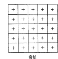
最基本的驱动方法是帧反相驱动方法,其中逐帧地对要施加到液晶单元帧上的电压极性进行反相,如日本专利公开No.平2-177679中所公开的。“帧”是向整个显示屏提供一个屏幕的数据信号所需的一个垂直扫描周期。图5A和5B是示出了当使用帧反相驱动方法时像素电极电压的正/负极性分布的图。图5A示出了在一个帧中的极性分布(被称为奇帧),而图5B示出了在图5A所示的奇帧之后的帧(被称为偶帧)的极性分布。The most basic driving method is the frame inversion driving method in which the polarity of the voltage to be applied to the liquid crystal cell frame is inverted frame by frame, as disclosed in Japanese Patent Laid-Open No. Hei 2-177679. A "frame" is a vertical scanning period required to provide a data signal of one screen to the entire display screen. 5A and 5B are graphs showing positive/negative polarity distribution of pixel electrode voltages when a frame inversion driving method is used. FIG. 5A shows the polarity distribution in one frame (referred to as an odd frame), while FIG. 5B shows the polarity distribution of a frame following the odd frame shown in FIG. 5A (referred to as an even frame).
图5A和5B所示的垂直方向与图4所示的作为栅极线的扫描方向的垂直方向匹配,而图5A和5B所示的水平方向与图4所示的栅极线延伸的水平方向匹配。图5A和5B所示的各个单元对应于图4所示的液晶单元5。对于标记为“+”的单元(液晶单元),像素电极的电位相对于公共电极的电位为正(此后简称为“正极性”)。对于标记为“-”的单元(液晶单元),像素电极的电位相对于公共电极的电位为负(此后简称为“负极性”)。根据帧反相驱动方法,如图5A和5B所示,当在一个帧中以正极性来驱动指定像素时,在下一帧中以负极性来驱动该像素。这可以确保液晶的寿命延长和高可靠性。The vertical direction shown in Figures 5A and 5B matches the vertical direction shown in Figure 4 as the scanning direction of the gate lines, while the horizontal direction shown in Figures 5A and 5B matches the horizontal direction in which the gate lines extend shown in Figure 4 match. Each cell shown in FIGS. 5A and 5B corresponds to the
然而,该帧反相驱动方法具有以下问题。如图5A和5B所示,当在一个帧中,要施加到液晶上的电压极性在整个显示屏上相同,则透射光量逐帧改变,引起了闪烁。换句话说,要施加到液晶上的电压由公共电极电压和像素电极电压之间的电位差来确定,并且当施加具有对称正和负极性的电压时,正极性模式下的光透射比变得等于负极性模式下的光透射比。当公共电极电位的中心电平与数据信号电位的中心电平略微偏移时,要施加到液晶上的电压的正和负极性变为非对称的,从而改变了正极性模式下的光透射比。当帧频率为60Hz时,液晶单元的光透射比的变化周期变为低至30Hz左右,从而观察者将其识别为闪烁。当在相对电极和数据线等之间进行电容耦合且相对电极自身具有电阻时,难以使相对电极的电位在整个屏幕上均是均匀的。即使当将相对电极的电位调节为最佳状态时,光透射比在正像素和负像素之间是不同的。However, this frame inversion driving method has the following problems. As shown in FIGS. 5A and 5B, when the polarity of the voltage to be applied to the liquid crystal is the same over the entire display screen in one frame, the amount of transmitted light changes frame by frame, causing flicker. In other words, the voltage to be applied to the liquid crystal is determined by the potential difference between the common electrode voltage and the pixel electrode voltage, and when voltages with symmetrical positive and negative polarities are applied, the light transmittance in the positive polarity mode becomes equal to Light transmittance in negative polarity mode. When the center level of the common electrode potential is slightly shifted from the center level of the data signal potential, the positive and negative polarities of the voltage to be applied to the liquid crystal become asymmetrical, thereby changing the light transmittance in the positive polarity mode. When the frame frequency is 60 Hz, the change period of the light transmittance of the liquid crystal cell becomes as low as about 30 Hz, so that the observer recognizes it as flicker. When capacitive coupling is performed between the opposing electrode and the data line or the like and the opposing electrode itself has resistance, it is difficult to make the potential of the opposing electrode uniform over the entire screen. Even when the potential of the opposite electrode is adjusted to an optimum state, light transmittance is different between positive and negative pixels.
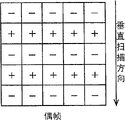
作为该问题的解决方案,例如,日本专利公开No.昭61-275823公开了一种栅极线反相驱动方法,用于对要施加到每一个扫描线上的液晶单元的电压极性进行反相。图6A和6B是示出了当使用栅极线反相驱动方法时像素电极电压的正/负极性分布的图。图6A示出了在一个奇帧中的极性分布,而图6B示出了在一个偶帧中的极性分布。图6A和6B所示的垂直方向和水平方向与图4和图5A和5B所示的垂直方向和水平方向匹配。As a solution to this problem, for example, Japanese Patent Laid-Open No. Sho 61-275823 discloses a gate line inversion driving method for inverting the polarity of a voltage to be applied to a liquid crystal cell on each scanning line. Mutually. 6A and 6B are graphs showing positive/negative polarity distribution of pixel electrode voltages when a gate line inversion driving method is used. FIG. 6A shows the polarity distribution in an odd frame, and FIG. 6B shows the polarity distribution in an even frame. The vertical and horizontal directions shown in FIGS. 6A and 6B match those shown in FIGS. 4 and 5A and 5B.
如图6A和6B所示,栅极线反相驱动方法逐栅极线地对每一个帧中的极性进行反相,并且逐帧地对每一个液晶单元的极性进行反相。因此,将正像素行和负像素行交替地排列在一个屏幕中,从而对垂直方向上的光透射比的变化进行平均,这能够减少闪烁。As shown in FIGS. 6A and 6B , the gate line inversion driving method inverts the polarity in each frame by gate line, and inverts the polarity of each liquid crystal cell by frame. Therefore, arranging positive pixel rows and negative pixel rows alternately in one screen, thereby averaging changes in light transmittance in the vertical direction, can reduce flicker.
日本专利公开No.昭63-68821公开了点反相驱动方法,用于对要施加到针对每一个相邻像素的液晶上的电压极性进行反相。图7A和7B是示出了当使用点反相驱动方法时像素电极电压的正/负极性分布的图。图7A示出了在奇帧中的极性分布,而图7B示出了在偶帧中的极性分布。图7A和7B所示的垂直方向和水平方向与图4和图5A和5B以及图6A和6B所示的垂直方向和水平方向匹配。Japanese Patent Laid-Open No. Sho 63-68821 discloses a dot inversion driving method for inverting the polarity of a voltage to be applied to liquid crystal for each adjacent pixel. 7A and 7B are graphs showing positive/negative polarity distribution of pixel electrode voltages when a dot inversion driving method is used. FIG. 7A shows the polarity distribution in odd frames, and FIG. 7B shows the polarity distribution in even frames. The vertical and horizontal directions shown in FIGS. 7A and 7B match those shown in FIGS. 4 and 5A and 5B and FIGS. 6A and 6B .
如图7A和7B所示,为了执行点反相驱动,按照使其极性针对在栅极线方向上相邻的每一个像素不同的方式,将数据信号提供给像素电极,并且按照使像素电极电压的极性针对在数据方向上相邻的每一个像素不同的方式,在每一个水平周期对数据信号的极性进行反相。因此,将正像素和负像素同时以垂直方向和水平方向交替排列在一个帧中,从而对整个屏幕上的光透射比的变化进行平均,消除了闪烁。As shown in FIGS. 7A and 7B, in order to perform dot inversion driving, a data signal is supplied to a pixel electrode in such a manner that its polarity is different for each pixel adjacent in the direction of the gate line, and the pixel electrode is supplied in such a manner that the pixel electrode The polarity of the voltage is different for each pixel adjacent in the data direction, and the polarity of the data signal is inverted every horizontal period. Therefore, positive pixels and negative pixels are alternately arranged in a frame in the vertical direction and the horizontal direction at the same time, so that the variation of light transmittance on the entire screen is averaged, and the flicker is eliminated.
在帧反相驱动方法、栅极线反相驱动方法和点反相驱动方法中,点反相驱动方法可以实现最佳图像质量。然而,栅极线反相驱动方法和点反相驱动方法需要在每一次栅极线驱动电路对单条栅极线进行扫描时,对数据线的极性进行反相,从而每一次反相时、对数据线、像素电极和公共电极进行充电和放电。这不必要地增加了能量消耗。在这一点上,例如,日本专利公开No.2001-215469公开了一种多栅极线反相驱动方法,作为帧反相驱动方法和栅极线反相驱动方法的一种折中。该方法用于通过对针对多条栅极线的每一个的像素电极电压的极性进行反相,实现闪烁的减少和对能量消耗的抑制。Among the frame inversion driving method, the gate line inversion driving method, and the dot inversion driving method, the dot inversion driving method can achieve the best image quality. However, the gate line inversion driving method and the dot inversion driving method need to invert the polarity of the data line each time the gate line driving circuit scans a single gate line, so that each time the phase inversion, Charge and discharge the data lines, pixel electrodes and common electrodes. This unnecessarily increases energy consumption. In this regard, for example, Japanese Patent Laid-Open No. 2001-215469 discloses a multi-gate line inversion driving method as a compromise between the frame inversion driving method and the gate line inversion driving method. This method is for achieving reduction of flicker and suppression of power consumption by inverting the polarity of a pixel electrode voltage for each of a plurality of gate lines.
然而,该传统技术具有以下问题。当在如图1和3所示的多视点图像显示设备中相对于多个视点来显示不同图像时,每一个图像的分辨率下降。例如,与二维图像显示模式相比,在立体图像中的分辨率变得更低。图8是图1所示的2视点视差屏障型图像显示设备的子像素的顶视图。However, this conventional technique has the following problems. When different images are displayed with respect to multiple viewpoints in the multi-viewpoint image display device as shown in FIGS. 1 and 3 , the resolution of each image decreases. For example, the resolution becomes lower in a stereoscopic image compared to a two-dimensional image display mode. FIG. 8 is a top view of sub-pixels of the 2-viewpoint parallax barrier type image display device shown in FIG. 1 .
如图8所示,立体图像模式下的一个显示像素包括二维图像显示模式下的两个显示像素。在立体图像模式下,两个显示像素变为用于显示针对左眼的图像的左眼像素和用于显示针对右眼的图像的右眼像素。左眼像素和右眼像素的每一个均包括三个原色子像素,并且三个狭长开口(slit opening)对应于一个显示像素。具体地,左眼红色子像素411和右眼绿色子像素422对应于第一狭长开口。左眼蓝色子像素413和右眼红色子像素421对应于下一狭长开口。左眼绿色子像素412和右眼蓝色子像素423对应于下一狭长开口。假定在狭长开口的长度方向(垂直方向11)上的原色子像素的布局间距是a,而在与狭长开口正交的方向(水平方向12)上的原色子像素的布局间距是b,则满足以下等式:As shown in FIG. 8 , one display pixel in the stereoscopic image mode includes two display pixels in the two-dimensional image display mode. In the stereoscopic image mode, two display pixels become a left-eye pixel for displaying an image for the left eye and a right-eye pixel for displaying an image for the right eye. Each of the left-eye pixel and the right-eye pixel includes three primary color sub-pixels, and three slit openings correspond to one display pixel. Specifically, the left-eye
(等式1)(equation 1)
a∶b=3∶1a:b=3:1
因此,针对狭长开口的长度方向上的立体图像模式下的显示像素间距a和与狭长开口的长度方向正交的方向上的显示像素间距b,满足以下等式2。即,在图8所示的立体图像显示设备显示立体图像时,一个显示像素在狭长开口的长度方向上具有尺寸a,在与长度方向正交的方向上具有尺寸b。Therefore, the following
(等式2)(equation 2)
a∶c=1∶2a:c=1:2
在图8所示的立体图像显示设备显示二维图像时,去除视差屏障105,并且将立体图像模式下的一个显示像素用作两个显示像素。去除视差屏障的方法公开于前述文献“Nikkei Electronics No.838,第26到27页,发布于2003年1月6日”中,其中视差屏障由用于开关的液晶板构成,并且改变液晶板的每一个元素的光透射比。当使用双凸透镜替代视差屏障时,通过改变显示板和双凸透镜之间的距离可以消除双凸透镜的效果。When the stereoscopic image display device shown in FIG. 8 displays a two-dimensional image, the
具体地,在二维图像显示模式下,将三个子像素,即左眼红色子像素411、右眼绿色子像素422和左眼蓝色子像素413用作单个显示像素,而将三个子像素,即右眼红色子像素421、左眼绿色子像素412和右眼蓝色子像素423用作单个显示像素。结果,一个显示像素在狭长开口的长度方向上具有尺寸a而在与长度方向正交的方向上具有尺寸(c/2)。然而,这只不过使与长度方向正交的方向上的像素间距加倍。因此,按照在由Sangyo Tosho出版有限公司出版的ChihiroMasuda等人所写的文献“Three-dimension Display”中所述的立体图像显示设备,将水平方向12的分辨率在立体图像模式下比在二维图像显示模式下减小一半。Specifically, in the two-dimensional image display mode, three sub-pixels, namely, the left-eye
当显示包含字符信息的立体图像时和当立体地显示字符信息时,分辨率的减小特别重要。当显示像素的形状变为高宽比为1∶2的矩形形状时,水平分辨率下降,从而当显示字符时,构成字符元素的垂直线部分下降。结果,字符显示的可视性显著下降。随着视点数量的增加,该问题变得显著。Reduction in resolution is particularly important when displaying a stereoscopic image containing character information and when displaying character information stereoscopically. When the shape of the display pixel is changed to a rectangular shape with an aspect ratio of 1:2, the horizontal resolution is lowered so that when a character is displayed, the vertical line portion constituting the character element is lowered. As a result, the visibility of character display is significantly reduced. This problem becomes significant as the number of viewpoints increases.
根据关于立体图像显示设备的现有技术,在整个屏幕上实现立体显示和二维显示之间的切换,并且不能够在任意位置处显示立体图像和二维图像的混合图像。According to the prior art on a stereoscopic image display device, switching between stereoscopic display and two-dimensional display is realized on the entire screen, and a mixed image of a stereoscopic image and a two-dimensional image cannot be displayed at an arbitrary position.
在用于显示多个视点的图像的显示设备中通常会出现仅对于立体图像显示设备并非固有的类似问题。即,当针对多个视点对不同图像进行显示时,针对多个视点的子像素的布局方向上的图像分辨率与其中显示单个图像的情况相比变得更低,并且可视性显著降低,特别是当显示字符时。Similar problems that are not inherent only to stereoscopic image display devices often arise in display devices for displaying images from multiple viewpoints. That is, when different images are displayed for a plurality of viewpoints, the image resolution in the layout direction of the sub-pixels for the plurality of viewpoints becomes lower compared with the case where a single image is displayed, and the visibility is significantly reduced, Especially when displaying characters.
发明内容 Contents of the invention
因此,本发明的目的是提出一种当显示针对多个视点的不同图像时其分辨率不会下降的液晶显示设备、配备有该液晶显示设备的便携式设备、以及针对液晶显示设备的驱动方法。Accordingly, an object of the present invention is to provide a liquid crystal display device whose resolution does not drop when displaying different images for a plurality of viewpoints, a portable device equipped with the liquid crystal display device, and a driving method for the liquid crystal display device.
根据本发明的第一液晶显示设备包括:像素电路衬底、与所述像素电路衬底平行且分离地设置的相对衬底、以及设置在像素电路衬底和相对衬底之间的液晶层。A first liquid crystal display device according to the present invention includes a pixel circuit substrate, an opposite substrate provided parallel to and separated from the pixel circuit substrate, and a liquid crystal layer provided between the pixel circuit substrate and the opposite substrate.
所述像素电路衬底包括:第一衬底;设置在所述第一衬底上并沿第一方向延伸的栅极线;设置在所述第一衬底上并沿与所述第一方向相交的第二方向延伸的数据线;分别设置在所述栅极线和所述数据线的最近点处的像素电极;开关元件,分别设置在所述最近点处,用于根据所述栅极线的电位来选择是否将所述数据线与所述像素电极相连;以及驱动电路,用于依次将栅极线驱动信号施加到所述栅极线上,所述栅极线驱动信号使与所述栅极线相连的所述开关元件导通,并且将数据信号输出到所述数据线。所述相对衬底包括第二衬底、以及设置在第二衬底上的公共电极。The pixel circuit substrate includes: a first substrate; a gate line arranged on the first substrate and extending along a first direction; a gate line arranged on the first substrate and extending along the first direction Intersecting data lines extending in the second direction; pixel electrodes respectively arranged at the nearest points of the gate lines and the data lines; line potential to select whether to connect the data line to the pixel electrode; The switching element connected to the gate line is turned on, and outputs a data signal to the data line. The opposite substrate includes a second substrate and a common electrode disposed on the second substrate.
每一个所述像素电极构成了子像素,(M×N)个(N和M分别是等于或大于2的整数)子像素构成了显示像素,其中N个子像素连续设置在所述第一方向上而M个子像素连续设置在所述第二方向上。每一个所述显示像素的所述(M×N)个子像素排列在方形区域中。每一次当将所述栅极线驱动信号施加到所述栅极线中的2到(2×M)条栅极线上时,所述驱动电路改变所述数据信号的电位相对于所述公共电极的电位的极性,并且逐帧地改变所述极性;Each of the pixel electrodes constitutes a sub-pixel, and (M×N) (N and M are integers equal to or greater than 2, respectively) sub-pixels constitute a display pixel, wherein N sub-pixels are continuously arranged in the first direction And M sub-pixels are continuously arranged in the second direction. The (M×N) sub-pixels of each display pixel are arranged in a square area. The drive circuit changes the potential of the data signal relative to the common the polarity of the potential of the electrodes, and changing said polarity frame by frame;
根据本发明,由于将(M×N)个子像素排列在每一个显示像素中,与用于将光线引导到N个视点的光学构件组合地使用该设备可以显示针对N个实现的不同图像。当显示针对N个视点的不同图像时,将不同图像显示在显示像素中沿第一方向排列的N个子像素上,并且当显示针对N个视点的彼此相同的图像时,将相同图像显示在沿第一方向排列的N个子像素上,从而使显示对N个视点的不同图像时的分辨率等于显示对N个视点的相同图像时的分辨率。即使当显示对N个视点的不同图像时,与其中显示对N个视点的相同图像的情况相比,分辨率也不会下降。由于当显示对N个视点的不同图像时的显示像素的数量等于当显示相同图像时的显示像素的数量,因此将两个图像混合在一个屏幕中。另外,将构成显示像素的(M×N)个子像素排列在方形区域中,图像的可视性较高且极佳,特别是当显示字符时。According to the present invention, since (M×N) sub-pixels are arranged in each display pixel, the device can display different images for N realizations using the device in combination with an optical member for directing light to N viewpoints. When displaying different images for N viewpoints, the different images are displayed on N subpixels arranged in the first direction among the display pixels, and when mutually identical images for N viewpoints are displayed, the same images are displayed along the On the N sub-pixels arranged in the first direction, the resolution when displaying different images for N viewpoints is equal to the resolution when displaying the same image for N viewpoints. Even when different images for N viewpoints are displayed, the resolution does not drop compared to a case where the same image for N viewpoints is displayed. Since the number of display pixels when displaying different images for N viewpoints is equal to the number of display pixels when displaying the same image, two images are mixed in one screen. In addition, by arranging (M×N) sub-pixels constituting a display pixel in a square area, the visibility of an image is high and excellent, especially when displaying characters.
根据本发明,由于M个子像素沿第二方向排列在每一个显示像素中,与具有沿第二方向排列在每一个显示像素的单个子像素的液晶显示设备相比,栅极线的数量更大。因此,使用栅极线反相驱动方法作为驱动方法增加了能量消耗并缩短了每一条栅极线的施加信号电压的时间,由此出现了不充分的信号电压充电。作为比较,使用帧反相驱动方法作为驱动方法使得闪烁很可能会出现。因此,根据本发明,每一次当驱动电路将栅极线驱动信号施加到2到(2×M)条栅极线上时,数据信号的电位相对于公共电极的电位的极性会发生改变,并且该极性逐帧地发生改变。这可以防止闪烁的出现并抑制能量消耗的增加和不充分的信号电压充电的出现。According to the present invention, since M sub-pixels are arranged in each display pixel along the second direction, the number of gate lines is larger compared with a liquid crystal display device having a single sub-pixel arranged in each display pixel along the second direction . Therefore, using the gate line inversion driving method as a driving method increases power consumption and shortens the signal voltage application time of each gate line, whereby insufficient signal voltage charging occurs. For comparison, using the frame inversion driving method as the driving method makes flicker likely to occur. Therefore, according to the present invention, every time when the driving circuit applies the gate line driving signal to 2 to (2×M) gate lines, the polarity of the potential of the data signal with respect to the potential of the common electrode changes, And the polarity changes frame by frame. This can prevent occurrence of flicker and suppress increase in power consumption and occurrence of insufficient signal voltage charging.
根据本发明的第二液晶显示设备包括:像素电路衬底、与所述像素电路衬底平行且分离地设置的相对衬底、以及设置在像素电路衬底和相对衬底之间的液晶层、以及滤色器。A second liquid crystal display device according to the present invention includes: a pixel circuit substrate, an opposite substrate disposed parallel to and separately from the pixel circuit substrate, and a liquid crystal layer disposed between the pixel circuit substrate and the opposite substrate, and color filters.
所述像素电路衬底包括:第一衬底;设置在所述第一衬底上并沿第一方向延伸的栅极线;设置在所述第一衬底上并沿与所述第一方向相交的第二方向延伸的数据线;分别设置在所述栅极线和所述数据线的最近点处的像素电极;开关元件,分别设置在所述最近点处,用于根据所述栅极线的电位来选择是否将所述数据线与所述像素电极相连;以及驱动电路,用于依次将栅极线驱动信号施加到所述栅极线上,所述栅极线驱动信号使与所述栅极线相连的所述开关元件导通,并且将数据信号输出到所述数据线。所述相对衬底包括第二衬底、以及设置在第二衬底上的公共电极。The pixel circuit substrate includes: a first substrate; a gate line arranged on the first substrate and extending along a first direction; a gate line arranged on the first substrate and extending along the first direction Intersecting data lines extending in the second direction; pixel electrodes respectively arranged at the nearest points of the gate lines and the data lines; line potential to select whether to connect the data line to the pixel electrode; The switching element connected to the gate line is turned on, and outputs a data signal to the data line. The opposite substrate includes a second substrate and a common electrode disposed on the second substrate.
每一个所述像素电极构成了子像素,(M×N)个(N和M分别是等于或大于2的整数)子像素构成了显示像素,其中N个子像素连续设置在所述第一方向上而M个子像素连续设置在所述第二方向上。所述滤色器是M种颜色的条状滤色器,沿所述第一方向延伸且分别插入在通过沿第二方向排列的每一个所述M个子像素的光线路径中。每一次当将所述栅极线驱动信号施加到所述栅极线中的2到(2×M)条栅极线上时,所述驱动电路改变所述数据信号的电位相对于所述公共电极的电位的极性,并且逐帧地改变所述极性;Each of the pixel electrodes constitutes a sub-pixel, and (M×N) (N and M are integers equal to or greater than 2, respectively) sub-pixels constitute a display pixel, wherein N sub-pixels are continuously arranged in the first direction And M sub-pixels are continuously arranged in the second direction. The color filters are stripe-shaped color filters of M colors, extending along the first direction and respectively inserted in a light path passing through each of the M sub-pixels arranged along the second direction. The drive circuit changes the potential of the data signal relative to the common the polarity of the potential of the electrodes, and changing said polarity frame by frame;
根据本发明,由于将(M×N)个子像素排列在每一个显示像素中,与用于将光线引导到N个视点的光学构件组合地使用该设备可以显示针对N个实现的不同图像。当显示针对N个视点的不同图像时,将不同图像显示在显示像素中沿第一方向排列的N个子像素上,并且当显示针对N个视点的彼此相同的图像时,将相同图像显示在沿第一方向排列的N个子像素上,从而使显示对N个视点的不同图像时的分辨率等于显示对N个视点的相同图像时的分辨率。由于当显示对N个视点的不同图像时的显示像素的数量等于当显示相同图像时的显示像素的数量,因此将两个图像混合在一个屏幕中。According to the present invention, since (M×N) sub-pixels are arranged in each display pixel, the device can display different images for N realizations using the device in combination with an optical member for directing light to N viewpoints. When displaying different images for N viewpoints, the different images are displayed on N subpixels arranged in the first direction among the display pixels, and when mutually identical images for N viewpoints are displayed, the same images are displayed along the On the N sub-pixels arranged in the first direction, the resolution when displaying different images for N viewpoints is equal to the resolution when displaying the same image for N viewpoints. Since the number of display pixels when displaying different images for N viewpoints is equal to the number of display pixels when displaying the same image, two images are mixed in one screen.
根据本发明,由于M个子像素沿第二方向排列在每一个显示像素中,能够防止子像素沿第一方向的布局间距显著变小,并且防止高宽比变小。然而,根据本发明的液晶显示设备,与具有沿第二方向排列在每一个显示像素的单个子像素的液晶显示设备相比,栅极线的数量更大。因此,使用栅极线反相驱动方法作为驱动方法增加了能量消耗并缩短了每一条栅极线的施加信号电压的时间,由此出现了不充分的信号电压充电。作为比较,使用帧反相驱动方法作为驱动方法使得闪烁很可能会出现。因此,根据本发明,每一次当驱动电路将栅极线驱动信号施加到2到(2×M)条栅极线上时,数据信号相对于公共电极的极性会发生改变,并且数据信号相对于公共电极的极性逐帧地发生改变。这可以防止闪烁的出现并抑制能量消耗的增加和不充分的信号电压充电的出现。According to the present invention, since M sub-pixels are arranged in each display pixel along the second direction, the layout pitch of the sub-pixels along the first direction can be prevented from becoming significantly smaller, and the aspect ratio can be prevented from becoming smaller. However, according to the liquid crystal display device of the present invention, the number of gate lines is larger than that of a liquid crystal display device having a single sub-pixel arranged in each display pixel along the second direction. Therefore, using the gate line inversion driving method as a driving method increases power consumption and shortens the signal voltage application time of each gate line, whereby insufficient signal voltage charging occurs. For comparison, using the frame inversion driving method as the driving method makes flicker likely to occur. Therefore, according to the present invention, every time when the driving circuit applies the gate line driving signal to 2 to (2×M) gate lines, the polarity of the data signal with respect to the common electrode changes, and the data signal is relatively The polarity of the common electrode changes frame by frame. This can prevent occurrence of flicker and suppress increase in power consumption and occurrence of insufficient signal voltage charging.
优选地,该液晶显示设备还应该包括光学构件,用于在每一个所述显示像素中,将来自沿所述第一方向排列的所述N个子像素中的第n(n是从1到N的整数)子像素的光线引导到第N观察点上,或者引导从外部输入的光线从而使其通过所述第n子像素并向所述第n观察点传播。Preferably, the liquid crystal display device should also include an optical component, which is used to connect the nth (n is from 1 to N) of the N sub-pixels arranged along the first direction in each of the display pixels Integers of ) sub-pixels are guided to the Nth observation point, or light input from the outside is guided to pass through the nth subpixel and travel to the nth observation point.
根据本发明的第三液晶显示设备包括:像素电路衬底、与所述像素电路衬底平行且分离地设置的相对衬底、以及设置在像素电路衬底和相对衬底之间的液晶层、以及双凸透镜,具有沿所述第一方向设置的多个柱面透镜且将已经通过所述液晶层的光引导到不同方向上。A third liquid crystal display device according to the present invention includes: a pixel circuit substrate, an opposite substrate disposed parallel to and separately from the pixel circuit substrate, and a liquid crystal layer disposed between the pixel circuit substrate and the opposite substrate, And a lenticular lens having a plurality of cylindrical lenses arranged along the first direction and guiding the light having passed through the liquid crystal layer into different directions.
所述像素电路衬底包括:第一衬底;设置在所述第一衬底上并沿第一方向延伸的栅极线;设置在所述第一衬底上并沿与所述第一方向相交的第二方向延伸的数据线;分别设置在所述栅极线和所述数据线的最近点处的像素电极;开关元件,分别设置在所述最近点处,用于根据所述栅极线的电位来选择是否将所述数据线与所述像素电极相连;以及驱动电路,用于依次将栅极线驱动信号施加到所述栅极线上,所述栅极线驱动信号使与所述栅极线相连的所述开关元件导通,并且将数据信号输出到所述数据线。所述相对衬底包括第二衬底、设置在第二衬底上的公共电极。The pixel circuit substrate includes: a first substrate; a gate line arranged on the first substrate and extending along a first direction; a gate line arranged on the first substrate and extending along the first direction Intersecting data lines extending in the second direction; pixel electrodes respectively arranged at the nearest points of the gate lines and the data lines; line potential to select whether to connect the data line to the pixel electrode; The switching element connected to the gate line is turned on, and outputs a data signal to the data line. The opposite substrate includes a second substrate and a common electrode disposed on the second substrate.
每一个所述像素电极构成了子像素。(M×N)个(N和M分别是等于或大于2的整数)子像素构成了显示像素,其中N个子像素连续设置在所述第一方向上而M个子像素连续设置在所述第二方向上。所述柱面透镜是与沿所述第二方向定向的所述显示像素的列相关联设置的,假定所述显示像素沿所述第一方向的布局间距是P,所述柱面透镜的布局间距是L,所述子像素沿所述第一方向的布局间距是b,以及所述子像素沿所述第二方向的布局间距是a,则满足(a×M)∶(b×N)=L∶P。每一次当将所述栅极线驱动信号施加到所述栅极线中的2到(2×M)条栅极线上时,所述驱动电路改变所述数据信号的电位相对于所述公共电极的电位的极性,并且逐帧地改变所述极性。Each of the pixel electrodes constitutes a sub-pixel. (M×N) sub-pixels (N and M are integers equal to or greater than 2, respectively) constitute a display pixel, wherein N sub-pixels are continuously arranged in the first direction and M sub-pixels are continuously arranged in the second direction. direction. The cylindrical lenses are arranged in association with the columns of the display pixels oriented along the second direction, assuming that the layout pitch of the display pixels along the first direction is P, the layout of the cylindrical lenses The pitch is L, the layout pitch of the sub-pixels along the first direction is b, and the layout pitch of the sub-pixels along the second direction is a, then (a×M):(b×N) =L:P. The drive circuit changes the potential of the data signal relative to the common The polarity of the potential of the electrodes is changed frame by frame.
根据本发明,由于将(M×N)个子像素排列在每一个显示像素中,并且按照使每一个柱面透镜与显示像素的行相对应的方式来设置双凸透镜,与用于将光线引导到N个视点的光学构件组合地使用该设备可以显示针对N个实现的不同图像。当显示针对N个视点的不同图像时,将不同图像显示在显示像素中沿第一方向排列的N个子像素上,并且当显示针对N个视点的彼此相同的图像时,将相同图像显示在沿第一方向排列的N个子像素上,从而使显示对N个视点的不同图像时的分辨率等于显示对N个视点的相同图像时的分辨率。即使当显示对N个视点的不同图像时,与其中显示对N个视点的相同图像的情况相比,分辨率也不会下降。由于当显示对N个视点的不同图像时的显示像素的数量等于当显示相同图像时的显示像素的数量,因此将两个图像混合在一个屏幕中。另外,对构成显示像素的(M×N)个子像素进行排列,从而满足等式(a×M)∶(b×N)=L∶P,当观察者通过双凸透镜观看包括像素电路衬底、液晶层和相对衬底的液晶板时,每一个显示像素看起来类似于方形。因此,图像可视性较高并极佳,特别是当显示字符时。According to the present invention, since (M×N) sub-pixels are arranged in each display pixel, and the lenticular lens is arranged in such a manner that each cylindrical lens corresponds to a row of the display pixel, the The device can display different images for N realizations using the optical components of N viewpoints in combination. When displaying different images for N viewpoints, the different images are displayed on N subpixels arranged in the first direction among the display pixels, and when mutually identical images for N viewpoints are displayed, the same images are displayed along the On the N sub-pixels arranged in the first direction, the resolution when displaying different images for N viewpoints is equal to the resolution when displaying the same image for N viewpoints. Even when different images for N viewpoints are displayed, the resolution does not decrease compared to a case where the same image for N viewpoints is displayed. Since the number of display pixels when displaying different images for N viewpoints is equal to the number of display pixels when displaying the same image, two images are mixed in one screen. In addition, the (M×N) sub-pixels constituting the display pixel are arranged so as to satisfy the equation (a×M):(b×N)=L:P, when the observer looks through the lenticular lens including the pixel circuit substrate, When the liquid crystal layer and the liquid crystal panel are opposed to the substrate, each display pixel looks similar to a square. Therefore, image visibility is high and excellent, especially when characters are displayed.
根据本发明,由于M个子像素沿第二方向排列在每一个显示像素中,与具有沿第二方向排列在每一个显示像素的单个子像素的液晶显示设备相比,栅极线的数量更大。因此,使用栅极线反相驱动方法作为驱动方法增加了能量消耗并缩短了每一条栅极线的施加信号电压的时间,由此出现不充分的信号电压充电。作为比较,使用帧反相驱动方法作为驱动方法使得闪烁很可能会出现。因此,根据本发明,每一次当驱动电路将栅极线驱动信号施加到2到(2×M)条栅极线上时,数据信号相对于公共电极的极性会发生改变,并且数据信号相对于公共电极的极性逐帧地发生改变。这可以防止闪烁的出现并抑制能量消耗的增加和不充分的信号电压充电的出现。According to the present invention, since M sub-pixels are arranged in each display pixel along the second direction, the number of gate lines is larger compared with a liquid crystal display device having a single sub-pixel arranged in each display pixel along the second direction . Therefore, using the gate line inversion driving method as a driving method increases power consumption and shortens the signal voltage application time of each gate line, whereby insufficient signal voltage charging occurs. For comparison, using the frame inversion driving method as the driving method makes flicker likely to occur. Therefore, according to the present invention, every time when the driving circuit applies the gate line driving signal to 2 to (2×M) gate lines, the polarity of the data signal with respect to the common electrode changes, and the data signal is relatively The polarity of the common electrode changes frame by frame. This can prevent occurrence of flicker and suppress increase in power consumption and occurrence of insufficient signal voltage charging.
在第一到第三液晶显示设备中,在每一个显示像素中,沿第一方向排列的N个子像素之一可以形成针对左眼的图像,而另一子像素可以形成针对右眼的图像,从而显示立体图像。In the first to third liquid crystal display devices, in each display pixel, one of the N subpixels arranged in the first direction may form an image for a left eye, and the other subpixel may form an image for a right eye, A stereoscopic image is thereby displayed.
另外,优选地,每一次当所述驱动电路将所述栅极线驱动信号施加到所述栅极线中的M条栅极线上时,所述驱动电路改变所述数据信号相对于公共电极的所述极性。因此,第二方向上的极性切换间距变得等于显示像素的布局间距,从而使每一种色调中的极性反相周期变得彼此相等。这减小了每一种色调中的帧间的亮度差,从而能够更可靠地防止闪烁的出现。In addition, preferably, each time when the drive circuit applies the gate line drive signal to the M gate lines in the gate lines, the drive circuit changes the data signal relative to the common electrode of the polarity. Therefore, the polarity switching pitch in the second direction becomes equal to the layout pitch of display pixels, so that the polarity inversion periods in each hue become equal to each other. This reduces the difference in luminance between frames in each tone, making it possible to more reliably prevent the occurrence of flicker.
此外,优选地,改变所述数据信号相对于所述公共电极的所述极性应该通过改变所述数据信号的电位和要施加到所述公共电极上的电位来实现。与其中公共电极的电位固定的情况相比,这可以使数据信号的电位的波动范围更小。Furthermore, preferably, changing the polarity of the data signal with respect to the common electrode should be achieved by changing the potential of the data signal and the potential to be applied to the common electrode. This can make the fluctuation range of the potential of the data signal smaller than the case where the potential of the common electrode is fixed.
根据本发明的便携式设备包括所述液晶显示设备。A portable device according to the present invention includes the liquid crystal display device.
根据本发明的第一液晶显示设备驱动方法用于液晶显示设备,所述液晶显示设备具有由(M×N)个(N和M分别是等于或大于2的整数)子像素构成的多个显示像素,所述(M×N)个设置在方形区域中,从而使所述N个子像素连续设置在栅极线沿着其延伸的第一方向上而使所述M个子像素连续设置在数据线沿着其延伸的第二方向上,每一个所述子像素是针对每一个像素电极而设置的。所述第一驱动方法具有用于将一个图像显示在液晶显示设备上的第一帧、以及相对于第一帧通过对极性反相来显示另一图像的第二帧。在第一和第二帧中,依次将栅极线驱动信号施加到所述栅极线上,所述栅极线驱动信号使与所述栅极线相连的所述开关元件导通,将数据信号输出到所述数据线,并且每一次当将所述栅极线驱动信号施加到所述栅极线中的2到(2×M)条栅极线上时,改变所述数据信号的电位相对于所述公共电极的电位的极性。The first method for driving a liquid crystal display device according to the present invention is used in a liquid crystal display device having a plurality of display screens composed of (M×N) sub-pixels (N and M are integers equal to or greater than 2, respectively). The (M×N) pixels are arranged in a square area, so that the N sub-pixels are continuously arranged in the first direction along which the gate line extends and the M sub-pixels are continuously arranged in the data line In the second direction along which it extends, each of the sub-pixels is provided for each pixel electrode. The first driving method has a first frame for displaying one image on a liquid crystal display device, and a second frame for displaying another image by inverting polarity with respect to the first frame. In the first and second frames, a gate line driving signal is sequentially applied to the gate line, and the gate line driving signal turns on the switching element connected to the gate line, and turns on the data signals are output to the data lines, and the potential of the data signals is changed every time when the gate line driving signals are applied to 2 to (2×M) gate lines among the gate lines The polarity of the potential with respect to the common electrode.
根据本发明的第二液晶显示设备驱动方法用于液晶显示设备所述液晶显示设备具有由(M×N)个(N和M分别是等于或大于2的整数)子像素构成的多个显示像素,从而使所述N个子像素连续设置在栅极线沿着其延伸的第一方向上而使所述M个子像素连续设置在数据线沿着其延伸的第二方向上,每一个所述子像素是针对每一个像素电极而设置的,并且具有M种颜色的条状滤色器,所述滤色器沿所述第一方向延伸且分别插入在通过沿第二方向排列的每一个所述M个子像素的光线路径中。所述第二驱动方法具有用于将一个图像显示在液晶显示设备上的第一帧、以及相对于第一帧通过对极性反相来显示另一图像的第二帧。在第一和第二帧中,依次将栅极线驱动信号施加到所述栅极线上,所述栅极线驱动信号使与所述栅极线相连的所述开关元件导通,将数据信号输出到所述数据线,并且每一次当将所述栅极线驱动信号施加到所述栅极线中的2到(2×M)条栅极线上时,改变所述数据信号的电位相对于所述公共电极的电位的极性。The second liquid crystal display device driving method according to the present invention is used in a liquid crystal display device having a plurality of display pixels composed of (M×N) (N and M are integers equal to or greater than 2, respectively) sub-pixels , so that the N sub-pixels are continuously arranged in the first direction along which the gate line extends and the M sub-pixels are continuously arranged in the second direction along which the data line extends, and each of the sub-pixels A pixel is provided for each pixel electrode, and has strip-shaped color filters of M colors, and the color filters extend along the first direction and are respectively inserted through each of the color filters arranged along the second direction. In the light path of M sub-pixels. The second driving method has a first frame for displaying one image on the liquid crystal display device, and a second frame for displaying another image by inverting polarity with respect to the first frame. In the first and second frames, a gate line driving signal is sequentially applied to the gate line, and the gate line driving signal turns on the switching element connected to the gate line, and turns on the data signals are output to the data lines, and the potential of the data signals is changed every time when the gate line driving signals are applied to 2 to (2×M) gate lines among the gate lines The polarity of the potential with respect to the common electrode.
根据本发明的第三液晶显示设备驱动方法用于液晶显示设备,所述液晶显示设备具有由(M×N)个(N和M分别是等于或大于2的整数)子像素构成的多个显示像素,从而使所述N个子像素连续设置在栅极线沿着其延伸的第一方向上而使所述M个子像素连续设置在数据线沿着其延伸的第二方向上,每一个所述子像素是针对每一个像素电极而设置的,并且具有双凸透镜,所述双凸透镜由与沿所述第二方向定向的所述显示像素的列相关联设置的多个柱面透镜构成的,假定所述显示像素沿所述第一方向的布局间距是P,所述柱面透镜的布局间距是L,所述子像素沿所述第一方向的布局间距是b,以及所述子像素沿所述第二方向的布局间距是a,则满足(a×M)∶(b×N)=L∶P。所述第三驱动方法具有用于将一个图像显示在液晶显示设备上的第一帧、以及相对于第一帧通过对极性反相来显示另一图像的第二帧。在第一和第二帧中,依次将栅极线驱动信号施加到所述栅极线上,所述栅极线驱动信号使与所述栅极线相连的所述开关元件导通,将数据信号输出到所述数据线,并且每一次当将所述栅极线驱动信号施加到所述栅极线中的2到(2×M)条栅极线上时,改变所述数据信号的电位相对于所述公共电极的电位的极性。The third liquid crystal display device driving method according to the present invention is used in a liquid crystal display device having a plurality of display screens composed of (M×N) sub-pixels (N and M are integers equal to or greater than 2, respectively). pixels, so that the N sub-pixels are consecutively arranged in the first direction along which the gate line extends and the M sub-pixels are consecutively arranged in the second direction along which the data line extends, each of the a sub-pixel is provided for each pixel electrode, and has a lenticular lens constituted by a plurality of cylindrical lenses provided in association with a column of said display pixels oriented in said second direction, assuming The layout pitch of the display pixels along the first direction is P, the layout pitch of the cylindrical lenses is L, the layout pitch of the sub-pixels along the first direction is b, and the sub-pixels along the If the layout pitch in the second direction is a, then (a×M):(b×N)=L:P is satisfied. The third driving method has a first frame for displaying one image on the liquid crystal display device, and a second frame for displaying another image by inverting polarity with respect to the first frame. In the first and second frames, a gate line driving signal is sequentially applied to the gate line, and the gate line driving signal turns on the switching element connected to the gate line, and turns on the data signals are output to the data lines, and the potential of the data signals is changed every time when the gate line driving signals are applied to 2 to (2×M) gate lines among the gate lines The polarity of the potential with respect to the common electrode.
根据本发明,当显示针对N个视点的不同图像时,将不同图像显示在显示像素中沿第一方向排列的N个子像素上,并且当显示针对N个视点的彼此相同的图像时,将相同图像显示在沿第一方向排列的N个子像素上,从而使显示对N个视点的不同图像时的分辨率等于显示对N个视点的相同图像时的分辨率。每一次当驱动电路将栅极线驱动信号施加到2到(2×M)条栅极线上时,数据信号的电位相对于公共电极的电位的极性会发生改变,并且该极性逐帧地发生改变。这可以防止闪烁的出现并抑制能量消耗的增加和不充分的信号电压充电的出现。According to the present invention, when displaying different images for N viewpoints, the different images are displayed on N sub-pixels arranged in the first direction in the display pixel, and when the mutually identical images for N viewpoints are displayed, the same Images are displayed on N sub-pixels arranged along the first direction, so that the resolution when displaying different images for N viewpoints is equal to the resolution when displaying the same image for N viewpoints. Every time when the drive circuit applies the gate line drive signal to 2 to (2×M) gate lines, the polarity of the potential of the data signal with respect to the potential of the common electrode changes, and the polarity changes frame by frame changed. This can prevent occurrence of flicker and suppress increase in power consumption and occurrence of insufficient signal voltage charging.
附图说明 Description of drawings
图1是示出了使用视差屏障的立体图像显示方法的光学模型图;1 is an optical model diagram illustrating a stereoscopic image display method using a parallax barrier;
图2是示出了双凸透镜的透视图;FIG. 2 is a perspective view showing a lenticular lens;
图3是示出了使用双凸透镜的立体图像显示方法的光学模型图;3 is an optical model diagram illustrating a stereoscopic image display method using a lenticular lens;
图4是示出了有源矩阵型液晶显示设备的液晶显示板部分的电路图;4 is a circuit diagram showing a liquid crystal display panel portion of an active matrix type liquid crystal display device;
图5A和5B是示出了当使用帧反相驱动方法时的像素电极电压的正/负极性分布的图;图5A示出了在奇帧中的极性分布,而图5B示出了在偶帧中的极性分布;5A and 5B are graphs showing the positive/negative polarity distribution of the pixel electrode voltage when using the frame inversion driving method; FIG. 5A shows the polarity distribution in odd frames, and FIG. 5B shows the polarity distribution in Polarity distribution in even frames;
图6A和6B是示出了当使用栅极线反相驱动方法时的像素电极电压的正/负极性分布的图;图6A示出了在奇帧中的极性分布,而图6B示出了在偶帧中的极性分布;6A and 6B are graphs showing the positive/negative polarity distribution of the pixel electrode voltage when using the gate line inversion driving method; FIG. 6A shows the polarity distribution in an odd frame, and FIG. 6B shows Polarity distribution in even frames;
图7A和7B是示出了当使用点反相驱动方法时的像素电极电压的正/负极性分布的图;图7A示出了在奇帧中的极性分布,而图7B示出了在偶帧中的极性分布;7A and 7B are graphs showing the positive/negative polarity distribution of the pixel electrode voltage when using the dot inversion driving method; FIG. 7A shows the polarity distribution in odd frames, and FIG. 7B shows the polarity distribution in Polarity distribution in even frames;
图8是图1所示的2视点视差屏障型图像显示设备的顶视图;8 is a top view of the 2-viewpoint parallax barrier type image display device shown in FIG. 1;
图9是根据本发明第一实施例的液晶显示设备的方框图;9 is a block diagram of a liquid crystal display device according to a first embodiment of the present invention;
图10是示出了图9所示的液晶板的显示像素和子像素之间的关系的方框图;10 is a block diagram showing the relationship between display pixels and sub-pixels of the liquid crystal panel shown in FIG. 9;
图11是根据本实施例的液晶显示设备的子像素的布局间距的顶视图;11 is a top view of the layout pitch of sub-pixels of the liquid crystal display device according to the present embodiment;
图12是示出了根据本实施例的图像显示设备的透视图;FIG. 12 is a perspective view showing an image display device according to the present embodiment;
图13是示出了液晶显示设备的操作的时序图,其中水平轴上取时间,而在垂直轴上取公共电极的电位VCOM、栅极线Y(3n+1)到Y(3n+4)的电位;13 is a timing chart showing the operation of the liquid crystal display device, in which time is taken on the horizontal axis and potential VCOM of the common electrode, gate lines Y(3n+1) to Y(3n+4) are taken on the vertical axis. potential;
图14A和14B是示出了本实施例中的像素电极电压的正/负极性分布的图;图14A示出了奇帧中的极性分布,而图14B示出了在偶帧中的极性分布;14A and 14B are graphs showing the positive/negative polarity distribution of the pixel electrode voltage in this embodiment; FIG. 14A shows the polarity distribution in an odd frame, and FIG. 14B shows the polarity distribution in an even frame. sex distribution;
图15是示出了作为根据本实施例的便携式设备的移动电话的透视图;FIG. 15 is a perspective view showing a mobile phone as a portable device according to the present embodiment;
图16是根据本发明第二实施例的液晶显示设备的液晶板的方框图;16 is a block diagram of a liquid crystal panel of a liquid crystal display device according to a second embodiment of the present invention;
图17是示出了根据本发明第三实施例的液晶显示设备的光学模型图;以及17 is an optical model diagram showing a liquid crystal display device according to a third embodiment of the present invention; and
图18是根据参考示例的液晶显示设备的液晶板的方框图。18 is a block diagram of a liquid crystal panel of a liquid crystal display device according to a reference example.
具体实施方式 Detailed ways
下面将参考附图来描述本发明的优选实施例。Preferred embodiments of the present invention will be described below with reference to the accompanying drawings.
(第一实施例)(first embodiment)
开始,将描述本发明的第一实施例。图9是根据本实施例的液晶显示设备的方框图;图10是示出了图9所示的液晶板的显示像素和子像素之间的关系的方框图;图11是示出了根据本实施例的液晶显示设备的子像素的布局间距的顶视图;以及图1 2是示出了根据本实施例的图像显示设备的透视图。Initially, a first embodiment of the present invention will be described. 9 is a block diagram of a liquid crystal display device according to the present embodiment; FIG. 10 is a block diagram showing the relationship between display pixels and sub-pixels of the liquid crystal panel shown in FIG. 9 ; A top view of layout pitches of sub-pixels of a liquid crystal display device; and FIG. 12 is a perspective view showing an image display device according to this embodiment.
如图9所示,根据本实施例的液晶显示设备具有液晶显示板1、栅极线驱动电路8和数据线驱动电路9,栅极线驱动电路8和数据线驱动电路9与液晶显示板1相连。按照使其与栅极线驱动电路8和数据线驱动电路9相连的方式来设置控制电路16。按照使其与控制电路16相连的方式来设置电源电路17和逻辑电路18。按照使其与逻辑电路18相连的方式来设置图像处理电路19。栅极线驱动电路8、数据线驱动电路9和控制电路16构成了液晶显示板1的驱动电路。As shown in FIG. 9, the liquid crystal display device according to this embodiment has a liquid
图像处理电路19包括处理器、存储器和对与外部电路输入/输出信号进行接口的接口电路(未示出)。图像处理电路19向逻辑电路18发送控制信号,例如同步信号和视频数据。The image processing circuit 19 includes a processor, a memory, and an interface circuit (not shown) that interfaces input/output signals with external circuits. The image processing circuit 19 sends control signals, such as synchronization signals and video data, to the logic circuit 18 .
逻辑电路18根据从图像处理电路19输入的视频数据和控制信号,产生用于驱动液晶显示板1的定时控制信号、以及视频数据DIN,并将其发送到控制电路16。电源电路17向控制电路16提供各种电源电位。Logic circuit 18 generates timing control signals for driving liquid
向控制电路16提供来自逻辑电路18的视频数据DIN和定时控制信号,并向控制电路16提供来自电源电路17的电源电压VCOM、逻辑部分电源电压、驱动部分电源电压和灰度电源电压。控制电路16根据该视频数据DIN和定时控制信号来改变电压电平,并将电平改变后的电压发送到栅极线驱动电路8和数据线驱动电路9。控制电路16向栅极线驱动电路8发送信号GST、时钟信号GCLK和其他控制信号,并向数据线驱动电路9发送视频信号DOUT、信号DST、时钟信号DCLK和其他控制信号。The control circuit 16 is supplied with the video data DIN and the timing control signal from the logic circuit 18 , and the control circuit 16 is supplied with the power supply voltage VCOM from the power supply circuit 17 , the logic section power supply voltage, the driving section power supply voltage and the grayscale power supply voltage. The control circuit 16 changes the voltage level according to the video data DIN and the timing control signal, and sends the level-changed voltage to the gate
栅极线驱动电路8包括移位寄存器(未示出)。当从控制电路16向其提供表示显示帧的起始点的信号GST时,对栅极线驱动电路8进行初始化,并且该栅极线驱动电路8与从控制电路16提供的时钟信号GCLK同步地将脉冲驱动电压施加到栅极线3上,从而顺序地驱动这些栅极线。此时,其中脉冲栅极驱动电压转换(turn)TFT 4的周期是将数据信号电压施加到液晶单元5中的时间。The gate
数据线驱动电路9包括移位寄存器、锁存电路和驱动电路(未示出)。数据线驱动电路9根据从控制电路16提供的信号DST,开始将视频信号DOUT提取到移位寄存器,与时钟信号DCLK同步地将视频信号DOUT顺序地提取到移位寄存器中,并且当提取了针对一条扫描线的视频信号时,停止将信号提取到移位寄存器中。数据线驱动电路9与从控制电路16提供的控制信号同步地将所提取的视频信号传送到锁存电路,并且将与视频信号相对应的信号电压经由驱动电路发送到数据线2。数据线驱动电路9将两个电平的参考电位提供给公共电极7。The data line driving circuit 9 includes a shift register, a latch circuit and a driving circuit (not shown). The data line drive circuit 9 starts extracting the video signal DOUT into the shift register in accordance with the signal DST supplied from the control circuit 16, sequentially extracts the video signal DOUT into the shift register in synchronization with the clock signal DCLK, and when extracted for When there is a video signal of one scan line, stop extracting the signal into the shift register. The data line driving circuit 9 transfers the extracted video signal to the latch circuit in synchronization with the control signal supplied from the control circuit 16, and sends a signal voltage corresponding to the video signal to the
下面将详细描述液晶显示板1的结构。液晶显示板1的电路结构与图4所示的传统液晶显示设备的液晶显示板1的结构相同。即,如图9所示,液晶显示板1具有彼此平行且分离地设置的像素电路衬底和相对衬底(未示出)、以及设置在其间的液晶层(未示出)。像素电路衬底具有像素电路衬底具有玻璃等透明衬底、设置在透明衬底上且以水平方向延伸的多条栅极线3、以及设置在透明衬底上且以垂直方向延伸的多条数据线2。液晶显示板1的栅极线3的一端与栅极线驱动电路8相连,而数据线的一端与数据线驱动电路9相连。The structure of the liquid
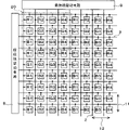
将TFT 4设置在每一条数据线2和每一条栅极线3的最近点处。栅极线3与TFT 4的栅极相连,数据线2与TFT 4的源极和漏极之一相连,而像素电极15与TFT 4的源极和漏极的另一个相连。根据栅极线3的电位使TFT 4导通或截止,以便选择性地将数据线2与像素电极15相连或将像素电极15设置为浮置。存储电容器6与像素电极15相连,所述存储电容器6保持在一个显示周期期间的信号电压。相对衬底具有公共电极7。液晶单元5由像素电路衬底的每一个像素电极15、相对衬底的公共电极7的面向像素电极15的该部分、以及液晶层的位于其间的该部分形成。液晶单元5显示针对一个点的子像素,并且构成电容器,用于保持要从数据线驱动电路9通过数据线2提供的数据信号的电位(施加的信号电压)。存储电容器6将用于保持信号电压的电容器添加到液晶单元5上,并且与液晶单元5并联以减小源自于寄生电容器的馈通电压。The
液晶显示板1的分辨率符合诸如HVGA(半视频图形阵列:80垂直×320水平),例如,显示区的高宽比(垂直尺寸与水平尺寸的比)是诸如3∶2,并且帧频率例如为60Hz。The resolution of the liquid
如图10所示,将显示像素10按照矩阵形式排列在液晶显示板1上。每一个显示像素10包括6个子像素。具体地,一个显示像素10包括在图10中从左边开始的液晶显示板1上的第(2m+1)子像素和第(2m+2)子像素、以及从顶部开始的第(3n+1)到第(3n+3)子像素。每一个子像素对应于图9所示的每一个液晶单元5。在液晶显示板1上,例如,从图中的左边开始的第(2m+1)数据线2由“X(2m+1)”来表示,而从图中的顶部开始的第(3n+1)栅极线3由“Y(3n+1)”来表示。在本实施例中,存在320条数据线2和1440条栅极线3。因此,m是范围从0到159的整数而n是范围从0到479的整数。As shown in FIG. 10 , the
如图10和11所示,在从图中的左边开始的液晶显示板1上的第(2m+1)列中重复设置从图中的顶部开始的红色左眼子像素RL、绿色左眼子像素GL和蓝色左眼子像素BL;而在第(2m+2)列中重复设置从图中的顶部开始的红色右眼子像素RR、绿色右眼子像素GR和蓝色右眼子像素BR。即,在从图中的顶部开始的第(3n+1)行中交替设置从左边开始的红色左眼子像素RL和红色右眼子像素RR,在第(3n+2)行中交替设置从左边开始的绿色左眼子像素GL和绿色右眼子像素GR,以及在第(3n+3)行中交替设置从左边开始的蓝色左眼子像素BL和蓝色右眼子像素BR。在子像素之间设置光屏蔽部分14。As shown in FIGS. 10 and 11, red left-eye sub-pixels RL, green left-eye sub-pixels RL, and green left-eye sub-pixels from the top in the figure are repeatedly arranged in the (2m+1)th column on the liquid
将构成单个显示像素10的子像素RL、GL、BL、RR、GR和BR排列在方形区域中。假定在数据线2沿着其延伸的方向(垂直方向11)上的子像素的布局间距是a,在栅极线3沿着其延伸的方向(水平方向12)上的子像素的布局间距是b,垂直方向11上的一个显示像素10中排列的子像素的数量为M,以及水平方向12上的一个显示像素10中排列的子像素的数量为N,则a、b、M和N满足以下等式3。由于在本实施例中M=3且N=2,则可以将等式3重写为以下等式4。The subpixels RL, GL, BL, RR, GR, and BR constituting a
(等式3)(equation 3)
M×a=N×bM×a=N×b
(等式4)(equation 4)
a∶b=2∶3a:b=2:3
液晶显示板1具有红色(R)滤色器31、绿色(G)滤色器32和蓝色(B)滤色器33,沿水平方向12延伸。每一个滤色器具有带状形状。The liquid
如图12所示,将双凸透镜43设置在液晶板1的前面,即,设置在观察者一侧。双凸透镜43具有沿垂直方向11延伸且设置在水平方向12上的多个柱面透镜43a。每一个柱面透镜43a对应于在垂直方向11上排列的显示像素10的列。将背光(未示出)设置在液晶板1的背面。As shown in FIG. 12, the
现在将描述这样构造的根据本实施例的液晶显示设备的操作,即,用于根据本实施例的液晶显示设备的驱动方法。图13是示出了液晶显示设备的操作的时序图,其中水平轴上取时间,而在垂直轴上取公共电极的电位VCOM、栅极线Y(3n+1)到Y(3n+4)的电位。该栅极线Y(3n+1)到Y(3n+4)与图10所示的栅极线Y(3n+1)到Y(3n+4)相同。图14A和14B是示出了本实施例中的像素电极电压的正/负极性分布的图,图14A示出了奇帧中的极性分布,而图14B示出了在偶帧中的极性分布。图14A和14B中的符号与图5A和5B中的符号相同。The operation of the thus configured liquid crystal display device according to the present embodiment, that is, a driving method for the liquid crystal display device according to the present embodiment will now be described. 13 is a timing chart showing the operation of the liquid crystal display device, in which time is taken on the horizontal axis and potential VCOM of the common electrode, gate lines Y(3n+1) to Y(3n+4) are taken on the vertical axis. potential. The gate lines Y(3n+1) to Y(3n+4) are the same as the gate lines Y(3n+1) to Y(3n+4) shown in FIG. 10 . 14A and 14B are graphs showing the positive/negative polarity distribution of the pixel electrode voltage in this embodiment, FIG. 14A shows the polarity distribution in an odd frame, and FIG. 14B shows the polarity distribution in an even frame. sex distribution. The symbols in Figs. 14A and 14B are the same as those in Figs. 5A and 5B.
首先,背光将光照射到液晶板1上。然后,图像处理电路19将视频数据和诸如同步信号等控制信号发送到逻辑电路18。逻辑电路18根据视频信号和控制信号,产生用于驱动液晶显示板1的定时控制信号,并且将该定时控制信号和视频数据DIN一起发送到控制电路16。电源电路17向控制电路16提供各种电源电位。结果,控制电路16根据从逻辑电路18提供的视频数据DIN和定时控制信号、从电源电路17提供的电源电压VCOM、逻辑部分电源电压、驱动部分电源电压和灰度电源电压来改变电压电平。控制电路16将表示显示帧的起始点的信号GST、时钟信号GLCK、电源电压VDDG和VSSG、以及电源电位VCOM提供给栅极线驱动电路8,并且将视频信号DOUT、启动信号DST、时钟信号DCLK、电源电位VDDD和VSSD以及电源电位VCOM发送到数据线驱动电路9。First, the backlight irradiates light onto the
如图13和14A所示,数据线驱动电路9将极性反相脉冲信号施加到公共电极7,并且将高电平(VCOMH)电位设置为5V,而将低电平(VCOML)电位设置为0V,与数据信号的电位相反的极性。首先,将与电源电位VSSD相同的低电平电位(例如0V)施加到公共电极7上。将基于要在与栅极线Y(1)相连的每一个液晶单元5上显示的视频信号的电位(数据信号)施加到数据线X(1)到X(320)上。此时,将数据信号的电位设置为0到5V。当输入信号GST时,栅极线驱动电路8将高电平(VDDG)电位施加到栅极线Y(1)上。结果,与栅极线Y(1)相连的液晶单元5的TFT 4导通,将施加到栅极线上的数据信号经由TFT 4施加到显示像素15上,并且施加到液晶单元5和存储电容器6中。此时,利用作为参考的公共电极电位电位VCOM来确定要施加到液晶单元5上的数据信号的极性,从而使数据信号的电位极性变为正。As shown in FIGS. 13 and 14A, the data line driving circuit 9 applies a polarity inversion pulse signal to the common electrode 7, and sets the high level (VCOMH) potential to 5V, and sets the low level (VCOML) potential to 0V, the polarity opposite to the potential of the data signal. First, the same low-level potential (for example, 0 V) as the power supply potential VSSD is applied to the common electrode 7 . A potential (data signal) based on a video signal to be displayed on each
接下来,与时钟信号GCLK同步,栅极线驱动电路8将栅极线Y(1)的电位设置为低电平而将栅极线Y(2)的电位设置为高电平。数据线驱动电路9根据要显示在与栅极线Y(2)相连的液晶单元5上的视频信号,向每一条数据线施加数据信号。结果,将正数据信号电压施加到与栅极线Y(2)相连的液晶单元5中。然后,栅极线驱动电路8将栅极线Y(2)的电位设置为低,而将栅极线Y(3)的电位设置为高,并且数据线驱动电路9根据要在与栅极线Y(3)相连的液晶单元5上显示的视频信号,向每一条数据线施加数据信号。结果,将正数据信号电压施加到与栅极线Y(3)相连的液晶单元5中。Next, in synchronization with the clock signal GCLK, the gate
接下来,与时钟信号GCLK同步,栅极线驱动电路8将栅极线Y(3)的电位设置为低而将栅极线Y(4)的电位设置为高。此时,数据线驱动电路9向公共电极7施加高电平电位,例如与电源电位VDDD相同的5V。数据线驱动电路9还根据要在与栅极线Y(4)相连的液晶单元5上显示的视频信号,向每一条数据线施加数据信号。例如,数据信号的电位是5到0V。结果,数据线驱动电路9将相对于公共电极的电位具有负极性的数据信号施加到与栅极线Y(4)相连的液晶单元5的像素电极15上。同样,数据线驱动电路9将负极性的数据信号电压顺序地施加到与栅极线Y(5)和Y(6)相连的液晶单元5上。Next, in synchronization with the clock signal GCLK, the gate
在将数据信号电压施加到与栅极线Y(7)到Y(9)相连的液晶单元5时,数据线驱动电路9将0V的电位再次施加到公共电极7上,以便将正数据信号电压施加到液晶单元5。要施加到液晶单元5的数据信号的极性按照该方式每三条栅极线发生改变。当栅极线驱动电路8将高电平电位顺序地施加到栅极线Y(1)到栅极线Y(1440)以扫描栅极线时,数据线驱动电路9与扫描同步地将数据信号施加到与那些栅极线相连的液晶单元5上。这可以允许将信号顺序地施加到与栅极线Y(1)到Y(1440)相连的液晶单元5。其中栅极线驱动电路8执行对栅极线Y(1)到Y(1440)的单个扫描的周期的一个帧。当将信号施加到与栅极线Y(1440)相连的液晶单元5时,一个帧(奇帧)结束。When the data signal voltage is applied to the
接下来,栅极线驱动电路8将高电平信号再次施加到栅极线Y(1),并开始如图13和14B所示的对栅极线Y(1)到Y(1440)的扫描。换句话说,开始下一帧(偶帧)。此时,数据线驱动电路9向公共电极和每一个数据线施加与奇帧的极性相反极性的电位。因此,将负极性的数据信号施加到与栅极线Y(1)到Y(3)相连的液晶单元5,并且将正极性的数据信号施加到与栅极线Y(4)到Y(6)相连的液晶单元5。对于其他栅极线也是如此。按照该方式对提供给液晶单元5的数据信号的极性进行反相。即,当相对于公共电极电位VCOM负极性的数据信号施加到由第x帧(x是自然数)中的栅极线Y(3n+1)、Y(3n+2)和Y(3n+3)所选的显示像素时,将相对于公共电极电位VCOM正极性的数据信号施加到由第x+1帧中的栅极线Y(3n+1)、Y(3n+2)和Y(3n+3)所选的显示像素。Next, the gate
如图13所示,用于选择栅极线Y(3n+1)的周期T1、用于选择栅极线Y(3n+2)的周期T2、以及用于选择栅极线Y(3n+3)的周期T3是将数据信号电压施加到与那些栅极线相连的液晶单元5的有效周期,而用于每三个水平周期执行极性反相的针对公共电极电位VCOM的上升周期TA和下降周期TB是其中没有将任何数据施加到液晶单元5的无效周期。当在本实施例中帧频率是60Hz时,一个屏幕的显示周期是16.7ms(毫秒),并且当液晶显示板1的分辨率是HVGA且栅极线的总数是1440时,一个水平周期是11.6μs(微秒)。当公共电极电位VCOM的反相周期由三个水平周期构成时,其变为34.7μs。假定使公共电极电位VCOM变得稳定的上升周期TA和下降周期TB是10μs,例如,三个水平周期中的10μs是无效周期而24.7μs是将数据信号施加到针对三个栅极线的像素的有效周期。As shown in FIG. 13, period T1 for selecting gate line Y(3n+1), period T2 for selecting gate line Y(3n+2), and period T2 for selecting gate line Y(3n+3) ) period T3 is an effective period for applying the data signal voltage to the
理想地,用于将数据信号电压施加到红色、绿色和蓝色的各种颜色的子像素的针对栅极线Y(3n+1)的选择周期T1、针对栅极线Y(3n+2)的选择周期T2、以及针对栅极线Y(3n+3)的选择周期T3应该全部相同,以便消除各种颜色的子像素之间的施加电压时间差。因此,根据本实施例,将数据信号施加到针对一个栅极线的像素的有效周期是8.24μs。Ideally, the selection period T1 for the gate line Y(3n+1), for the gate line Y(3n+2) The selection period T2 for the gate line Y(3n+3) and the selection period T3 for the gate line Y(3n+3) should all be the same, so as to eliminate the voltage application time difference between the sub-pixels of each color. Therefore, according to the present embodiment, the effective period for applying a data signal to pixels for one gate line is 8.24 μs.
当将0到5V的数据信号电压按照上述方式在每一帧中施加到液晶显示板1的所有液晶单元5时,根据电压透过液晶单元5的光透射比发生改变。因此,从背光发出的一些光线受到液晶单元5的阻碍,而剩余光线透过液晶单元5。已经通过液晶单元5的光线通过滤色器31到33以进行着色,并且由双凸透镜43以水平方向进行引导。当观察者将右眼和左眼移动到适当位置时,已经透过左眼子像素21到23的光线到达观察者的左眼,而已经透过右眼子像素24到26的光线到达观察者的右眼。When the data signal voltage of 0 to 5V is applied to all the
当在左眼子像素和右眼子像素上显示具有视差的图像时,观察者可以识别立体图像。即,液晶显示设备可以显示立体图像。当相同信息显示在左眼子像素和右眼子像素上时,可以显示二维图像。此时,该图像的分辨率与立体图像模式下的分辨率相同,并且显示像素的形状变为方形。When an image with parallax is displayed on the left-eye sub-pixel and the right-eye sub-pixel, a viewer can recognize a stereoscopic image. That is, the liquid crystal display device can display stereoscopic images. When the same information is displayed on the left-eye sub-pixel and the right-eye sub-pixel, a two-dimensional image can be displayed. At this point, the resolution of the image is the same as in stereoscopic mode, and the shape of the display pixels becomes square.
现在将描述根据本实施例的便携式设备。图15是示出了根据本实施例的作为便携式设备的移动电话。如图15所示,将根据本实施例的液晶显示设备42安装在根据本实施例的移动电话41中。液晶显示设备42具有上述结构。A portable device according to the present embodiment will now be described. FIG. 15 is a diagram showing a mobile phone as a portable device according to the present embodiment. As shown in FIG. 15, a liquid crystal display device 42 according to the present embodiment is installed in a mobile phone 41 according to the present embodiment. The liquid crystal display device 42 has the above-described structure.
下面将讨论本实施例的效果。根据本实施例,一个显示像素10具有6个子像素,红色左眼子像素RL、绿色左眼子像素GL、蓝色左眼子像素BL、红色右眼子像素RR、绿色右眼子像素GR、以及蓝色右眼子像素BR,从而还可以显示彩色立体图像。该显示像素在显示立体图像时和显示二维图像时均为相同的。因此,与显示二维图像的情况相比,当显示立体图像时分辨率不会下降。另外,可以在一个屏幕中混合地显示二维图像和立体图像。在这种情况下,两个图像的分辨率也是彼此相等的,从而观察者不会感到难看。The effect of this embodiment will be discussed below. According to this embodiment, one
当垂直方向11上的每一个子像素的宽度a与水平方向12上的每一个子像素的宽度b的比值为2∶3时,显示像素的形状变为方形。因此,立体图像模式下的显示像素的形状变为方形。这实现了极佳的图像可视性。当将字符信息显示为立体图像时,效果特别好。这是由于当垂直和水平分辨率下降时,作为字符信息的构成元素的垂直线或水平线丢失(drop out),使得观察者极其难以识别字符信息。因此,使垂直分辨率等于水平分辨率可以尤其确保对字符信息的适当立体显示。When the ratio of the width a of each sub-pixel in the
当在本实施例中设置了在水平方向12上延伸的带状滤色器31到33时,可以沿垂直方向11来排列三个子像素,而沿水平方向12来排列两个子像素。因此,可以使所排列的子像素散布在垂直方向和水平方向上,以便与在水平方向12上布置6个子像素的情况相比,使水平方向上的子像素的密度松弛,从而能够增加孔径比且便于液晶板的制造。When the
注意,在本实施例中,在垂直方向11上每个显示像素三个子像素的布置将栅极线的数量增加为传统数量的三倍大。当设置了在垂直方向上延伸的红色滤色器且将各个颜色的子像素按照水平方向排列在传统彩色液晶显示设备中时,栅极线的数量与单色液晶显示设备相同。因此,使用栅极线反相驱动方法或点反相驱动方法来驱动本实施例的液晶显示设备显著地增加了能量消耗,并缩短了每一条栅极线的施加信号电压的时间,从而引起了错误地保持信号电压。另一方面,使用帧反相驱动方法可能会引起闪烁。Note that in this embodiment, the arrangement of three sub-pixels per display pixel in the
因此,根据本实施例,如以上所讨论的,每三条栅极线对数据信号的极性进行反相。该方案防止了闪烁的出现,并且能够确保每一条栅极线8.24μs的施加信号电压的时间,能够抑制能量消耗的增加和错误地保持信号的出现。当将传统栅极线反相驱动方法适用于具有与本实施例相同像素结构的液晶板时,一个水平周期变为11.6μs。假定使公共电极电位VCOM稳定的周期如同本实施例那样为10μs,每一条栅极线的施加信号电压的时间变为1.6μs,短于本实施例中的8.24μs。这样短的施加电压时间极其难以可靠地向液晶单元施加电压。Therefore, according to the present embodiment, as discussed above, the polarity of the data signal is inverted every three gate lines. This solution prevents the occurrence of flicker, and can ensure the time of applying the signal voltage of 8.24 μs to each gate line, and can suppress the increase of energy consumption and the occurrence of erroneously holding the signal. When the traditional gate line inversion driving method is applied to a liquid crystal panel having the same pixel structure as that of this embodiment, one horizontal period becomes 11.6 μs. Assuming that the period for stabilizing the common electrode potential VCOM is 10 μs as in the present embodiment, the time for applying the signal voltage to each gate line becomes 1.6 μs, which is shorter than 8.24 μs in the present embodiment. Such a short voltage application time is extremely difficult to reliably apply voltage to the liquid crystal cell.
当每三条栅极线或每一个显示像素(一个像素)对数据信号的极性进行反相时,减小了每一种色调中的帧间的亮度差,从而可以确定地防止闪烁的出现。换句话说,能够抑制能量消耗的增加和错误保持信号电压的出现,同时通过每两条栅极线或每四条栅极线对数据信号的极性进行反相,防止了闪烁的出现,每三条栅极线对极性进行反相可以允许将极性均匀地分配给红色子像素、绿色子像素和蓝色子像素,从而在显示像素之间不会出现亮度差,并且在每一种色调中的帧间的亮度差会减少。这能够可靠地防止闪烁的出现并进一步改善图像质量。When the polarity of the data signal is inverted every three gate lines or every display pixel (one pixel), the difference in luminance between frames in each tone is reduced, so that the occurrence of flicker can be surely prevented. In other words, it is possible to suppress the increase in power consumption and the occurrence of false hold signal voltage, while preventing the occurrence of flicker by inverting the polarity of the data signal every two gate lines or every four gate lines, every three gate lines Inverting the polarity of the gate lines allows the polarity to be evenly distributed to the red, green, and blue subpixels so that there is no brightness difference between display pixels and in each hue The brightness difference between frames will be reduced. This can reliably prevent occurrence of flicker and further improve image quality.
在本实施例中,将AC电压施加到公共电极,并且通过改变数据信号的电位和公共电极的电位来改变数据信号的极性。与其中公共电极的电位固定而仅改变数据信号的电位的情况相比,这可以使数据信号的电位的变化更小。结果,可以降低液晶显示设备的各个电组件的击穿电压,引起了设备成本的降低。In this embodiment, an AC voltage is applied to the common electrode, and the polarity of the data signal is changed by changing the potential of the data signal and the potential of the common electrode. This can make the change in the potential of the data signal smaller than in the case where the potential of the common electrode is fixed and only the potential of the data signal is changed. As a result, the breakdown voltage of each electrical component of the liquid crystal display device can be reduced, leading to a reduction in device cost.
尽管本发明前面的描述仅给出了将两个(N=2)子像素水平排列在每一个显示像素中且显示彼此具有视差的右眼图像和左眼图像以提供立体显示的示例,但是本发明并不局限于该特定示例,而可以应用于其中相对于两个视点来显示不同图像的液晶显示设备。在将二维不同图像显示为N个视点处的图像的多视点显示的情况下,可以使显示像素的形状成为方形。这可以防止二维图像的分辨率的下降,并且特别是能够提高字符显示的可视性。Although the foregoing description of the present invention has only given an example in which two (N=2) sub-pixels are horizontally arranged in each display pixel and display a right-eye image and a left-eye image with parallax to each other to provide a stereoscopic display, the present invention The invention is not limited to this specific example, but can be applied to a liquid crystal display device in which different images are displayed with respect to two viewpoints. In the case of multi-viewpoint display in which two-dimensionally different images are displayed as images at N viewpoints, the shape of the display pixels can be made square. This can prevent a decrease in the resolution of the two-dimensional image, and in particular, can improve the visibility of character display.
(第二实施例)(second embodiment)
接下来,现在将解释本发明的第二实施例。图16是示出了根据本实施例的液晶显示设备的液晶显示板的方框图。如图16所示,本实施例与第一实施例的不同在于:每一个显示像素20包括十二个子像素。即,在垂直方向11上以红色、绿色和蓝色的次序,在液晶板1上重复设置沿水平方向12延伸的红色、绿色和蓝色的带状滤色器。将双凸透镜(未示出)设置在液晶板1的正面。构成双凸透镜的多个柱面透镜沿垂直方向11延伸,并且一个柱面透镜对应于沿水平方向12连续设置在一个显示像素中的四个子像素。Next, a second embodiment of the present invention will now be explained. FIG. 16 is a block diagram showing a liquid crystal display panel of the liquid crystal display device according to the present embodiment. As shown in FIG. 16 , the difference between this embodiment and the first embodiment is that each
结果,在每一个显示像素20中,在图中按照从左到右的次序将红色子像素R1到R4设置在图16所示的最顶行,按照从左到右的次序将绿色子像素G1到G4设置在从顶部开始的第二行,并按照从左到右的次序将蓝色子像素B1到B4设置在从顶部开始的第三行,即,最低一行。沿垂直方向设置在列中的子像素R1、G1和B1显示针对第一视点的图像。同样,沿垂直方向设置在列中的子像素R2、G2和B2显示针对第二视点的图像,子像素R3、G3和B3显示针对第三视点的图像,而子像素R4、G4和B4显示针对第四视点的图像。As a result, in each
在上述结构的一般性描述中,一个显示像素20包括:液晶显示板1上从图16中的左边开始的第(4k+1)到第(4k+4)子像素、以及从顶部开始的第(3n+1)到第(3n+3)子像素,其中k是范围从0到159的整数。如从液晶板1的正面看到的,构成单个显示像素的十二个子像素排列在方形区域中。假定在垂直方向11上的子像素的布局间距是a,水平方向12上的子像素的布局间距是b,在垂直方向11上、一个显示像素20中所设置的子像素的数量为M,以及在水平方向12上、一个显示像素20中所设置的子像素的数量为N,则a、b、M和N满足等式3。由于在本实施例中M=3且N=4,因此可以将等式3重写为以下等式5。本实施例的其他结构与第一实施例的相应结构相同。In the general description of the above structure, one
(等式5)(equation 5)
a∶b=4∶3a:b=4:3
接下来,现在将解释如上所述结构的根据本实施例的液晶显示设备的操作,即针对根据本实施例的液晶显示设备的驱动方法。在本实施例中,在显示针对第一到第四视点的不同图像时,将针对第一视点的图像显示在第一组子像素R1、G1上;将针对第二视点的图像显示在第二组子像素R2、G2和B2上;将针对第三视点的图像显示在第三组子像素R3、G3和B3上;以及将针对第四视点的图像显示在第四组子像素R4、G4和B4上。可以按照该方式来实现多视点显示。在显示针对第一到第四视点的相同图像时,在第一到第四组上相互显示该相同图像。即,子像素R1到R4由相同信号来驱动;子像素G1到G4由相同信号来驱动;以及子像素B1到B4由相同信号来驱动。除了以上所述操作之外的本实施例的其他操作与第一实施例的相应操作相同。即,每三个水平周期且逐帧地对数据信号的极性进行反相。Next, the operation of the liquid crystal display device according to the present embodiment structured as described above, that is, the driving method for the liquid crystal display device according to the present embodiment will now be explained. In this embodiment, when displaying different images for the first to fourth viewpoints, the image for the first viewpoint is displayed on the first group of sub-pixels R1, G1; the image for the second viewpoint is displayed on the second group of sub-pixels R2, G2 and B2; images for the third viewpoint are displayed on the third group of sub-pixels R3, G3 and B3; and images for the fourth viewpoint are displayed on the fourth group of sub-pixels R4, G4 and on B4. Multi-viewpoint display can be realized in this way. When displaying the same image for the first to fourth viewpoints, the same image is mutually displayed on the first to fourth groups. That is, the sub-pixels R1 to R4 are driven by the same signal; the sub-pixels G1 to G4 are driven by the same signal; and the sub-pixels B1 to B4 are driven by the same signal. Other operations of this embodiment other than those described above are the same as the corresponding operations of the first embodiment. That is, the polarity of the data signal is inverted every three horizontal periods and frame by frame.
接下来,现在将解释本实施例的效果。在本实施例中,当将红色子像素R1到R4、绿色子像素G1到G4和蓝色子像素B1到B4这十二个子像素设置在一个显示像素20中时,可以显示针对四个视点的彩色图像。即使显示针对四个视点的不同图像、或显示相同图像,这些图像的分辨率也不会改变。因此,可以在一个屏幕中对不同图像和相同图像进行混合,并且该混合不会引起难看的感觉。由于每一个显示像素的形状是方形,图像的可视性极佳,并且特别是字符信息的可视性极佳。除了上述之外的本实施例的其他效果与第一实施例相同。Next, effects of the present embodiment will now be explained. In this embodiment, when twelve sub-pixels of red sub-pixels R1 to R4, green sub-pixels G1 to G4, and blue sub-pixels B1 to B4 are arranged in one
在本实施例中,当显示针对四个视点的不同图像时,可以显示针对四个视点的相互无关的图像,可以显示针对四个视点中的两个视点的彼此具有视差的针对右眼的图像和针对左眼的图像,从而可以显示立体图像,或者可以单独地显示两个立体图像集合,一个集合针对四个视点中的两个,而另一集合针对其余两个视点。In this embodiment, when displaying different images for four viewpoints, mutually unrelated images for the four viewpoints may be displayed, and images for the right eye with mutual parallax for two of the four viewpoints may be displayed and an image for the left eye so that a stereoscopic image can be displayed, or two sets of stereoscopic images can be displayed separately, one set for two of the four viewpoints and the other for the remaining two viewpoints.
(第三实施例)(third embodiment)
接下来,现在将描述本发明的第三实施例。图17是根据本实施例的液晶显示设备的光学模型图。本实施例与第一实施例的不同在于:液晶板中的显示像素的布局间距不同于双凸透镜中的柱面透镜的布局间距。即,将多个显示像素以矩阵形式排列在液晶板上,每一个显示像素具有六个子像素,两个显示像素排列在水平方向上而三个显示像素排列在垂直方向上,如同第一实施例。将背光44设置在液晶板1的背面。Next, a third embodiment of the present invention will now be described. FIG. 17 is an optical model diagram of the liquid crystal display device according to the present embodiment. The difference between this embodiment and the first embodiment lies in that the layout pitch of the display pixels in the liquid crystal panel is different from the layout pitch of the cylindrical lenses in the lenticular lens. That is, a plurality of display pixels are arranged in a matrix on the liquid crystal panel, each display pixel has six sub-pixels, two display pixels are arranged in the horizontal direction and three display pixels are arranged in the vertical direction, as in the first embodiment . A
如图11和17所示,假定在每一个显示像素中沿垂直方向11排列的子像素的数量为M,沿水平方向12排列的子像素的数量为N,垂直方向11上的子像素的布局间距是a,水平方向12上的子像素的布局间距是b,水平方向12上的显示像素的布局间距是P,以及水平方向12上的柱面透镜的布局间距是L,则满足以下等式6。在本实施例中,由于N=2且M=3,则可以将等式6重写为以下等式7。除了上述之外的本实施例的其他结构与第一实施例的相应结构相同。As shown in Figures 11 and 17, assuming that the number of sub-pixels arranged in the
(等式6)(equation 6)
(a×M)∶(b×N)=L∶P(a×M):(b×N)=L:P
(等式7)(Equation 7)
a∶b=(L/3)∶(P/2)a:b=(L/3):(P/2)
在本实施例中,从背光10中输出的光线透过左眼子像素(例如红色左眼子像素RL)和右眼子像素(例如,红色右眼子像素RR),并且透射的光由双凸透镜43的柱面透镜43a折射,并且分别到达观察者的左眼142和右眼141。此时,如果将具有相互视差的图像显示在左眼子像素和右眼子像素上,观察者可以识别立体图像。如果将相同图像同时显示在左眼子像素和右眼子像素上,则观察者可以识别二维图像。In this embodiment, the light output from the
在本实施例中,由于显示像素的垂直长度变为(a×M)而水平长度变为(b×N),因此其比值(高宽比)满足等式6。当观察者通过双凸透镜43来观看液晶板1时,如在水平方向12上以(L/P)倍放大或缩小地那样观察显示像素。至于垂直方向11,以相等的放大倍数来观察显示像素。因此,当观察者通过双凸透镜43观看液晶板1时的显示像素的表观高宽比变为垂直∶水平=(a×M)∶{(b×N)×(L/P)}=L∶{P×(L/P)}=1∶1并且将显示像素看作方形。由此,即使液晶板中的显示像素的布局间距不同于双凸透镜中的柱面透镜的布局间距,本实施例也可以表现出与第一实施例相同的效果。本实施例的其他操作和效果与第一实施例相同。In this embodiment, since the vertical length of the display pixel becomes (a×M) and the horizontal length becomes (b×N), the ratio thereof (aspect ratio) satisfies
尽管前面对实施例的描述已经给出了其中作为示例、每一次当扫描三条栅极线时(即,每三个水平周期)对数据信号电位相对于公共电极电位的极性进行反相,但是本实施例并不局限于这种情况,并且可以在每一次当扫描2到(2×M)条栅极线时对极性进行反相,其中在每一个像素中沿垂直方向排列的子像素的数量为M。即,在每一个上述实施例中,由于M=3,可以每2到6个水平周期对极性进行反相。Although the foregoing description of the embodiment has been given as an example in which the polarity of the potential of the data signal with respect to the potential of the common electrode is inverted every time when three gate lines are scanned (that is, every three horizontal periods), But this embodiment is not limited to this case, and the polarity can be reversed every time when scanning 2 to (2×M) gate lines, wherein the sub-sections arranged in the vertical direction in each pixel The number of pixels is M. That is, in each of the above-mentioned embodiments, since M=3, the polarity can be inverted every 2 to 6 horizontal periods.
现在将解释针对以上情况的理由。当对数据线和公共电极的电位极性进行反相时,需要确保足够的时间来使数据线和公共电极的电位在设定值处变得稳定,这是因为由于数据线和公共电极的时间常数使得在上升时间处的波形变钝。如利用作为示例所给出的具体数字在第一实施例的描述中所解释地那样,当栅极线的总数较大时,如果通过应用栅极线反相驱动方法逐栅极线地使公共电极电压反相,则针对公共电极电位的时间相对于每一条栅极线的施加信号电压的时间变长,缩短了将数据信号施加到像素上的时间,很可能会引起不充分的施加电压。结果,如果当操作液晶显示板时针对每一条栅极线对极性进行反相,则能量消耗会变大,并且每一条栅极线的施加电压的时间会变得更短,可能会引起有错误地电压保持。因此,在本发明的液晶显示设备中,需要扫描至少两条栅极线,直到使数据信号的极性反相为止。The reason for the above case will now be explained. When inverting the potential polarity of the data line and the common electrode, it is necessary to ensure enough time for the potential of the data line and the common electrode to become stable at the set value, because due to the timing of the data line and the common electrode The constant dulls the waveform at the rise time. As explained in the description of the first embodiment using specific numbers given as examples, when the total number of gate lines is large, if the common When the electrode voltage is reversed, the time for applying the signal voltage to the common electrode potential becomes longer than the time for applying the signal voltage to each gate line, which shortens the time for applying the data signal to the pixel, possibly resulting in insufficient applied voltage. As a result, if the polarity is reversed for each gate line when operating the liquid crystal display panel, power consumption becomes larger and the time for applying voltage to each gate line becomes shorter, possibly causing unwanted Incorrect voltage hold. Therefore, in the liquid crystal display device of the present invention, at least two gate lines need to be scanned until the polarity of the data signal is inverted.
相反,如果每一次当扫描多于(2×M)条栅极线时对极性进行反相,由具有相同极性的子像素构成的区域的宽度(垂直长度)变大,并且具有不同极性的区域的空间混合度变小,从而使观察者将这些区域识别为水平条图案。因此,需要使由具有相同极性的子像素构成的区域的宽度小于或等于与(2×M)条栅极线相对应的区域。因此,在本发明中,每一次当扫描2到(2×M)条栅极线时,对极性进行反相。On the contrary, if the polarity is inverted every time when more than (2×M) gate lines are scanned, the width (vertical length) of the region composed of sub-pixels having the same polarity becomes large and has different poles. The degree of spatial mixing becomes less in the regions of contrast, allowing the observer to recognize these regions as a pattern of horizontal bars. Therefore, it is necessary to make the width of an area composed of sub-pixels having the same polarity smaller than or equal to an area corresponding to (2×M) gate lines. Therefore, in the present invention, the polarity is inverted every time when 2 to (2×M) gate lines are scanned.
如在前面对第一实施例的描述中所解释的,当每M到(2×M)条栅极线对极性进行反相时,可以使极性的反相间距和显示像素的布局间距彼此匹配,从而特别有效地防止闪烁的出现并尤其提高了显示质量。As explained above in the description of the first embodiment, when the polarity is reversed every M to (2×M) gate lines, the polarity reversal pitch and the layout of the display pixels can be made The distances are adapted to one another, so that the occurrence of flicker is prevented particularly effectively and the display quality is improved in particular.
尽管前面对本实施例的描述已经给出了将双凸透镜用作光学构件的情况,但是本发明并不局限于该情况,而可以诸如使用视差屏障。可以将该视差屏障设置在液晶板的正面或其背面,即,液晶板和背光之间。Although the foregoing description of the present embodiment has given the case where a lenticular lens is used as the optical member, the present invention is not limited to this case, and a parallax barrier may be used, for example. The parallax barrier may be placed on the front side of the liquid crystal panel or on the back side thereof, ie, between the liquid crystal panel and the backlight.
尽管前面对这些实施例的描述已经给出了使用透明液晶显示器的情况,但是本发明可以使用反射型液晶显示板。在使用反射型液晶显示板时,将类似于双凸透镜的光学构件设置在液晶板的正面,将透明衬底用作液晶板的正面衬底,并且将反射层设置在液晶层和背部衬底之间。因此,来自正面的输入光透过正面衬底和液晶层,并且在反射层处发生反射,并且再透过液晶层和正面衬底,使得图像得以添加。然后,由光学构件将光引导到多个视点。注意,在反射型液晶层中,背部衬底不必一定是透明的。在这种情况下,可以通过使显示像素排列在方形区域中来增强可视性,并且按照这些实施例,每一次当对2到(2×M)条栅极线进行扫描时,通过切换数据信号的极性来抑制能量消耗的增加。Although the foregoing descriptions of the embodiments have given the case of using a transparent liquid crystal display, the present invention can use a reflective liquid crystal display panel. When using a reflective liquid crystal display panel, an optical member similar to a lenticular lens is arranged on the front of the liquid crystal panel, a transparent substrate is used as the front substrate of the liquid crystal panel, and a reflective layer is arranged between the liquid crystal layer and the back substrate between. Therefore, input light from the front side passes through the front substrate and the liquid crystal layer, and is reflected at the reflective layer, and then passes through the liquid crystal layer and the front substrate, so that an image is added. The light is then directed to multiple viewpoints by the optical member. Note that in a reflective liquid crystal layer, the back substrate does not have to be transparent. In this case, visibility can be enhanced by arranging display pixels in a square area, and according to these embodiments, each time when scanning 2 to (2×M) gate lines, by switching data The polarity of the signal to suppress the increase in power consumption.
尽管前面对这些实施例的描述已经作为示例给出了针对两个视点或四个视点的液晶显示设备,但是本发明并不局限于这种情况,并且可以应用于针对N个视点的液晶显示设备(N是大于或等于2的整数)。Although the foregoing descriptions of these embodiments have given an example of a liquid crystal display device for two viewpoints or four viewpoints, the present invention is not limited to this case, and can be applied to a liquid crystal display device for N viewpoints device (N is an integer greater than or equal to 2).
尽管前面对这些实施例的描述已经给出了其中将三个子像素以垂直方向排列在每一个显示像素中(即M=3)作为红色、绿色和蓝色子像素的情况,但是本发明并不局限于这种情况,并且可以将两种颜色或四种或更多颜色的子像素设置在每一个显示像素中。Although the foregoing descriptions of these embodiments have given the case in which three sub-pixels are vertically arranged in each display pixel (that is, M=3) as red, green and blue sub-pixels, the present invention does not It is not limited to this case, and sub-pixels of two colors or four or more colors may be provided in each display pixel.
尽管前面对这些实施例的描述已经给出了其中将TFT用作开关元件的情况,但是本发明并不局限于该情况,而可以使用除了TFT之外的其他开关元件。在这种情况下,栅极线充当用于传送用于使开关元件导通和断开的切换信号的线。Although the foregoing descriptions of the embodiments have given the case in which TFTs are used as switching elements, the present invention is not limited to this case and switching elements other than TFTs may be used. In this case, the gate line serves as a line for transmitting a switching signal for turning on and off the switching element.
尽管示出了作为便携式设备的移动电话,但是本发明并不局限于该情况,并且可以将第一实施例的液晶显示设备安装到移动终端、PDA、游戏机、数字摄像机或数字视频上。可以将第二或第三实施例的液晶显示设备安装到这些便携式设备上。本发明的液晶显示设备可以用作针对个人计算机等的专用监视器。在这种情况下,可以将图9所示的图像处理电路19设置在个人计算机中。Although a mobile phone is shown as a portable device, the present invention is not limited to this case, and the liquid crystal display device of the first embodiment may be mounted on a mobile terminal, PDA, game machine, digital video camera, or digital video. The liquid crystal display device of the second or third embodiment can be mounted to these portable devices. The liquid crystal display device of the present invention can be used as a dedicated monitor for a personal computer or the like. In this case, the image processing circuit 19 shown in FIG. 9 can be provided in a personal computer.
Claims (6)
Applications Claiming Priority (3)
| Application Number | Priority Date | Filing Date | Title |
|---|---|---|---|
| JP2004-208230 | 2004-07-15 | ||
| JP2004208230A JP4572095B2 (en) | 2004-07-15 | 2004-07-15 | Liquid crystal display device, portable device, and driving method of liquid crystal display device |
| JP2004208230 | 2004-07-15 |
Related Child Applications (1)
| Application Number | Title | Priority Date | Filing Date |
|---|---|---|---|
| CN2008102126390A Division CN101339315B (en) | 2004-07-15 | 2005-07-14 | liquid crystal display device |
Publications (2)
| Publication Number | Publication Date |
|---|---|
| CN1721961A CN1721961A (en) | 2006-01-18 |
| CN100426110C true CN100426110C (en) | 2008-10-15 |
Family
ID=35598953
Family Applications (2)
| Application Number | Title | Priority Date | Filing Date |
|---|---|---|---|
| CN2008102126390A Expired - Lifetime CN101339315B (en) | 2004-07-15 | 2005-07-14 | liquid crystal display device |
| CNB2005100846815A Expired - Lifetime CN100426110C (en) | 2004-07-15 | 2005-07-14 | Liquid crystal display device, portable device, and driving method of liquid crystal display device |
Family Applications Before (1)
| Application Number | Title | Priority Date | Filing Date |
|---|---|---|---|
| CN2008102126390A Expired - Lifetime CN101339315B (en) | 2004-07-15 | 2005-07-14 | liquid crystal display device |
Country Status (3)
| Country | Link |
|---|---|
| US (2) | US20060012593A1 (en) |
| JP (1) | JP4572095B2 (en) |
| CN (2) | CN101339315B (en) |
Cited By (1)
| Publication number | Priority date | Publication date | Assignee | Title |
|---|---|---|---|---|
| CN101339315B (en) * | 2004-07-15 | 2011-05-25 | Nec液晶技术株式会社 | liquid crystal display device |
Families Citing this family (87)
| Publication number | Priority date | Publication date | Assignee | Title |
|---|---|---|---|---|
| JP2003337303A (en) * | 2002-05-17 | 2003-11-28 | Canon Inc | Stereoscopic image display device and stereoscopic image display system |
| WO2006100950A1 (en) * | 2005-03-22 | 2006-09-28 | Sharp Kabushiki Kaisha | Display apparatus, circuit for driving the same, and method for driving the same |
| WO2006100951A1 (en) * | 2005-03-22 | 2006-09-28 | Sharp Kabushiki Kaisha | Circuit for driving display apparatus and method for driving display apparatus |
| KR20070043314A (en) * | 2005-10-21 | 2007-04-25 | 삼성전자주식회사 | Liquid crystal display device |
| DE102006031757A1 (en) * | 2006-01-04 | 2007-08-02 | Arnold & Richter Cine Technik Gmbh & Co. Betriebs Kg | Method for automatically correcting image errors in video assist images of a video assist system |
| KR101320637B1 (en) * | 2006-01-23 | 2013-11-13 | (주)쓰리디아이에스 | Stereoscopic Image Display Apparatus of Net Pattern |
| JP4998914B2 (en) * | 2006-05-10 | 2012-08-15 | ソニーモバイルディスプレイ株式会社 | Liquid crystal display |
| KR20080006362A (en) * | 2006-07-12 | 2008-01-16 | 삼성전자주식회사 | Driving method of display device |
| JP2008134617A (en) | 2006-10-23 | 2008-06-12 | Nec Lcd Technologies Ltd | Display device, terminal device, display panel, and optical member |
| CN101201498A (en) * | 2006-10-23 | 2008-06-18 | Nec液晶技术株式会社 | Display device, terminal device, display panel and optical member |
| JP4966022B2 (en) * | 2007-01-05 | 2012-07-04 | 株式会社ジャパンディスプレイセントラル | Flat display device and control method thereof |
| KR101351379B1 (en) * | 2007-02-01 | 2014-01-14 | 엘지디스플레이 주식회사 | Liquid crystal display device |
| CN101681607B (en) * | 2007-06-06 | 2012-11-21 | 夏普株式会社 | Display unit and drive method thereof |
| TWI378433B (en) * | 2007-08-16 | 2012-12-01 | Tpo Displays Corp | Control method and electronic system utilizing the same |
| JP2009048000A (en) * | 2007-08-21 | 2009-03-05 | Toshiba Matsushita Display Technology Co Ltd | Liquid crystal display device |
| CN101377904B (en) * | 2007-08-31 | 2011-12-14 | 群康科技(深圳)有限公司 | Liquid crystal display device and driving method thereof |
| JP4478899B2 (en) * | 2007-10-15 | 2010-06-09 | Nec液晶テクノロジー株式会社 | Display device, terminal device, display panel, and driving method of display device |
| US8446355B2 (en) | 2007-10-15 | 2013-05-21 | Nlt Technologies, Ltd. | Display device, terminal device, display panel, and display device driving method |
| KR100918698B1 (en) * | 2007-11-20 | 2009-09-22 | 주식회사 실리콘웍스 | Offset Compensation Gamma Buffer and Gray-Voltage Generation Circuit Using the Same |
| KR101465220B1 (en) * | 2007-11-29 | 2014-11-26 | 엘지디스플레이 주식회사 | Dual view display device and its image implementation method |
| JP2010088087A (en) * | 2008-10-03 | 2010-04-15 | Seiko Epson Corp | Electro-optical device, and electronic apparatus |
| JP5472781B2 (en) | 2008-10-08 | 2014-04-16 | Nltテクノロジー株式会社 | Shift register, display device, and shift register driving method |
| KR100995065B1 (en) * | 2009-01-12 | 2010-11-18 | 삼성모바일디스플레이주식회사 | Display device |
| TWI419124B (en) * | 2009-03-06 | 2013-12-11 | Au Optronics Corp | 2d/3d image displaying apparatus |
| KR101323090B1 (en) * | 2009-03-11 | 2013-10-29 | 엘지디스플레이 주식회사 | Liquid crystal display and driving method thereof |
| CN101762902B (en) * | 2009-03-13 | 2013-04-24 | 深超光电(深圳)有限公司 | Liquid crystal display panel with high picture quality |
| US8797231B2 (en) * | 2009-04-15 | 2014-08-05 | Nlt Technologies, Ltd. | Display controller, display device, image processing method, and image processing program for a multiple viewpoint display |
| KR101354329B1 (en) * | 2009-04-17 | 2014-01-22 | 엘지디스플레이 주식회사 | Image display device |
| WO2010134409A1 (en) * | 2009-05-22 | 2010-11-25 | シャープ株式会社 | Stereoscopic display device |
| KR101570142B1 (en) * | 2009-08-25 | 2015-11-20 | 삼성전자주식회사 | Liquid crystal display apparatus and driving method of liquid crystal display apparatus |
| KR20110024970A (en) | 2009-09-03 | 2011-03-09 | 삼성전자주식회사 | Stereoscopic display |
| JP5603042B2 (en) * | 2009-09-14 | 2014-10-08 | 株式会社有沢製作所 | Stereoscopic image display device |
| KR101588347B1 (en) * | 2009-09-28 | 2016-01-26 | 삼성디스플레이 주식회사 | Liquid crystal display panel, liquid crystal display device including same, and driving method of liquid crystal display device |
| CN102577405B (en) * | 2009-11-03 | 2015-05-20 | 皇家飞利浦电子股份有限公司 | Autostereoscopic display device and method for controlling autostereoscopic display device |
| KR101325302B1 (en) * | 2009-11-30 | 2013-11-08 | 엘지디스플레이 주식회사 | Stereoscopic image display and driving method thereof |
| TW201129078A (en) * | 2010-02-01 | 2011-08-16 | Chunghwa Picture Tubes Ltd | Stereoscopic image displaying method |
| MX2012011461A (en) * | 2010-04-08 | 2012-11-29 | Sharp Kk | Liquid-crystal display device and three-dimensional display system. |
| JP4920104B2 (en) | 2010-08-06 | 2012-04-18 | 株式会社東芝 | 3D image display device and display method |
| JP4865069B1 (en) | 2010-08-06 | 2012-02-01 | 株式会社東芝 | 3D image display device and display method |
| KR101236519B1 (en) * | 2010-08-06 | 2013-02-21 | 엘지디스플레이 주식회사 | Stereoscopic image display and driving method thereof |
| JP2012093503A (en) * | 2010-10-26 | 2012-05-17 | Sony Corp | Stereoscopic image display apparatus |
| JP6010291B2 (en) | 2010-11-05 | 2016-10-19 | 株式会社半導体エネルギー研究所 | Driving method of display device |
| JP5728895B2 (en) * | 2010-11-09 | 2015-06-03 | セイコーエプソン株式会社 | Electro-optical device and electronic apparatus |
| KR101753262B1 (en) | 2010-11-17 | 2017-07-04 | 삼성디스플레이 주식회사 | Display apparatus and method of driving the same |
| JP2012118338A (en) * | 2010-12-01 | 2012-06-21 | Sharp Corp | Liquid crystal display device, stereoscopic display system, control program and recording medium |
| KR101296902B1 (en) * | 2010-12-08 | 2013-08-14 | 엘지디스플레이 주식회사 | Image processing unit and stereoscopic image display device using the same, and image processing method |
| JP4892098B1 (en) * | 2010-12-14 | 2012-03-07 | 株式会社東芝 | 3D image display apparatus and method |
| KR101804890B1 (en) * | 2010-12-23 | 2017-12-06 | 삼성디스플레이 주식회사 | Method of driving display panel and a display apparatus performing the method |
| TWI431606B (en) * | 2010-12-31 | 2014-03-21 | Au Optronics Corp | 3d display and driving method thereof |
| JP5900818B2 (en) * | 2011-03-29 | 2016-04-06 | Nltテクノロジー株式会社 | Liquid crystal display |
| TWI425498B (en) * | 2011-05-04 | 2014-02-01 | Au Optronics Corp | Video-audio playing system relating to 2-views application and method thereof |
| KR101292249B1 (en) * | 2011-05-18 | 2013-08-02 | 삼성디스플레이 주식회사 | Display apparatus |
| KR101818567B1 (en) * | 2011-05-18 | 2018-02-22 | 삼성디스플레이 주식회사 | Method of driving display panel and display apparatus performing the method |
| WO2012177073A2 (en) | 2011-06-24 | 2012-12-27 | 엘지전자 주식회사 | Method for transmitting uplink control information, user equipment, method for receiving uplink control information, and base station |
| CN102930809B (en) * | 2011-08-12 | 2016-02-10 | 上海中航光电子有限公司 | The transversely arranged dot structure that bigrid drives and display panel |
| KR101868145B1 (en) * | 2011-10-06 | 2018-06-18 | 엘지디스플레이 주식회사 | Stereoscopic image display |
| CN103135295B (en) * | 2011-11-29 | 2015-09-30 | 上海中航光电子有限公司 | The pixels across structure that bigrid drives and liquid crystal display |
| CN103149719B (en) * | 2011-12-06 | 2016-08-03 | 上海天马微电子有限公司 | Liquid crystal display panel, driving method thereof and liquid crystal display |
| US8992024B2 (en) | 2012-01-25 | 2015-03-31 | International Business Machines Corporation | Three dimensional image projector with circular light polarization |
| US8960913B2 (en) | 2012-01-25 | 2015-02-24 | International Busniess Machines Corporation | Three dimensional image projector with two color imaging |
| US8985785B2 (en) | 2012-01-25 | 2015-03-24 | International Business Machines Corporation | Three dimensional laser image projector |
| US9004700B2 (en) | 2012-01-25 | 2015-04-14 | International Business Machines Corporation | Three dimensional image projector stabilization circuit |
| US9104048B2 (en) | 2012-01-25 | 2015-08-11 | International Business Machines Corporation | Three dimensional image projector with single modulator |
| US20130188149A1 (en) | 2012-01-25 | 2013-07-25 | International Business Machines Corporation | Three dimensional image projector |
| US9325977B2 (en) * | 2012-01-25 | 2016-04-26 | International Business Machines Corporation | Three dimensional LCD monitor display |
| CN102629041B (en) | 2012-02-09 | 2014-04-16 | 京东方科技集团股份有限公司 | Three-dimensional (3D) display device and manufacture method thereof |
| CN202487576U (en) | 2012-02-09 | 2012-10-10 | 京东方科技集团股份有限公司 | Array substrate and dual viewing field display device |
| KR20130105777A (en) * | 2012-03-16 | 2013-09-26 | 삼성디스플레이 주식회사 | Stereoscopic display |
| CN102637399B (en) * | 2012-04-27 | 2015-12-16 | 天马微电子股份有限公司 | Stereo-picture display proving installation and method |
| CN102856320B (en) * | 2012-08-13 | 2015-06-10 | 京东方科技集团股份有限公司 | TFT (thin film transistor) array substrate and display |
| JP6061266B2 (en) | 2012-10-19 | 2017-01-18 | Nltテクノロジー株式会社 | Liquid crystal display |
| JP5472840B2 (en) * | 2012-11-26 | 2014-04-16 | Nltテクノロジー株式会社 | Image display device and terminal device |
| JP6292464B2 (en) | 2013-06-20 | 2018-03-14 | Tianma Japan株式会社 | Display device |
| TWI519823B (en) * | 2013-08-29 | 2016-02-01 | 中華映管股份有限公司 | Autostereoscopic display panel, alignment method, and autostereoscopic display method thereof |
| US9336734B2 (en) * | 2013-12-25 | 2016-05-10 | Shenzhen China Star Optoelectronics Technology Co., Ltd. | Driving method for polarity inversion of data signal and image display method of liquid crystal panel |
| JP5812127B2 (en) * | 2014-02-03 | 2015-11-11 | 株式会社ニコン | Image playback device |
| CN104199193A (en) * | 2014-07-31 | 2014-12-10 | 京东方科技集团股份有限公司 | Display device capable of switching 2D display and 3D display |
| CN104597609A (en) | 2015-02-06 | 2015-05-06 | 京东方科技集团股份有限公司 | Pixel array, display device and display method |
| KR102486413B1 (en) * | 2016-06-15 | 2023-01-10 | 삼성디스플레이 주식회사 | Display panel and display apparatus including the same |
| KR102657989B1 (en) * | 2016-11-30 | 2024-04-16 | 삼성디스플레이 주식회사 | Display device |
| CN106875852B (en) * | 2017-02-27 | 2021-08-17 | 北京京东方光电科技有限公司 | A display substrate, a display panel, a display device and a display method thereof |
| CN106959483A (en) * | 2017-06-01 | 2017-07-18 | 宁波视睿迪光电有限公司 | A kind of Grating Film and 3 d display device |
| KR102699276B1 (en) * | 2018-08-08 | 2024-08-28 | 삼성디스플레이 주식회사 | Display device and method of driving the same |
| CN110459187B (en) * | 2019-08-15 | 2021-08-06 | 京东方科技集团股份有限公司 | Driving method, driving device and display device of transparent display |
| CN113805372B (en) * | 2020-06-16 | 2024-10-29 | 深圳光峰科技股份有限公司 | LCD panel and display device |
| CN115136227B (en) * | 2020-11-30 | 2023-11-17 | 京东方科技集团股份有限公司 | Display device and display method thereof |
| CN112505942B (en) * | 2021-02-03 | 2021-04-20 | 成都工业学院 | Multi-resolution stereoscopic display device based on rear projection light source |
Citations (6)
| Publication number | Priority date | Publication date | Assignee | Title |
|---|---|---|---|---|
| JPH0921979A (en) * | 1995-07-04 | 1997-01-21 | Canon Inc | Stereoscopic image display method and stereoscopic image display device using the same |
| US5833507A (en) * | 1995-07-04 | 1998-11-10 | Sharp Kabushiki Kaisha | Method of making an SLM, SLM, autostereoscopic display, and backlight |
| US5850269A (en) * | 1996-03-30 | 1998-12-15 | Samsung Electronics Co., Ltd. | Liquid crystal display device wherein each scanning electrode includes three gate lines corresponding separate pixels for displaying three dimensional image |
| CN1317778A (en) * | 2000-03-28 | 2001-10-17 | 瓦智能Bvi有限公司 | Driving method of liquid crystal display |
| JP2003177424A (en) * | 2001-12-12 | 2003-06-27 | Hitachi Ltd | Liquid crystal display |
| US6727878B2 (en) * | 2000-02-04 | 2004-04-27 | Nec Lcd Technologies, Ltd. | Liquid crystal display |
Family Cites Families (20)
| Publication number | Priority date | Publication date | Assignee | Title |
|---|---|---|---|---|
| JPS61275823A (en) | 1985-05-31 | 1986-12-05 | Seiko Epson Corp | liquid crystal display device |
| JPS6368821A (en) | 1986-09-11 | 1988-03-28 | Fujitsu Ltd | Driving method for active matrix type liquid crystal panel |
| JPH02177679A (en) | 1989-11-13 | 1990-07-10 | Seiko Epson Corp | liquid crystal display device |
| JPH052991A (en) | 1991-02-14 | 1993-01-08 | Toshiba Lighting & Technol Corp | Tube sealing method |
| JPH06332354A (en) | 1993-05-20 | 1994-12-02 | Toppan Printing Co Ltd | Display for simultaneously displaying plural images |
| JPH08248385A (en) * | 1995-03-08 | 1996-09-27 | Hitachi Ltd | Active matrix type liquid crystal display and its driving method |
| GB9513658D0 (en) * | 1995-07-05 | 1995-09-06 | Philips Electronics Uk Ltd | Autostereoscopic display apparatus |
| KR100218525B1 (en) * | 1995-12-29 | 1999-09-01 | 윤종용 | Driving method and circuit for display device of matrix type |
| JPH09251172A (en) * | 1996-03-18 | 1997-09-22 | Toshiba Electron Eng Corp | Active matrix type liquid crystal display device, driving method thereof, driving circuit and liquid crystal display system |
| JPH1032772A (en) * | 1996-07-17 | 1998-02-03 | Casio Comput Co Ltd | Liquid crystal display device and driving method thereof |
| US5899550A (en) * | 1996-08-26 | 1999-05-04 | Canon Kabushiki Kaisha | Display device having different arrangements of larger and smaller sub-color pixels |
| US20010011981A1 (en) * | 1996-12-27 | 2001-08-09 | Tsunenori Yamamoto | Active matrix addressed liquid crystal display device |
| US6061084A (en) * | 1998-01-21 | 2000-05-09 | New York University | Displayer and a method for displaying |
| WO2000021069A1 (en) | 1998-10-07 | 2000-04-13 | Microsoft Corporation | Mapping samples of foreground/background color image data to pixel sub-components |
| JP2002062855A (en) * | 2000-08-22 | 2002-02-28 | Texas Instr Japan Ltd | Driving method of liquid crystal display device |
| KR101017231B1 (en) * | 2002-10-30 | 2011-02-25 | 가부시키가이샤 한도오따이 에네루기 켄큐쇼 | Display device and electronic device |
| JP4400172B2 (en) * | 2003-02-28 | 2010-01-20 | 日本電気株式会社 | Image display device, portable terminal device, display panel, and image display method |
| JP4200056B2 (en) * | 2003-06-17 | 2008-12-24 | 有限会社シーフォン | Display device |
| KR100689311B1 (en) * | 2003-11-10 | 2007-03-08 | 엘지.필립스 엘시디 주식회사 | LCD and its driving method |
| JP4572095B2 (en) * | 2004-07-15 | 2010-10-27 | Nec液晶テクノロジー株式会社 | Liquid crystal display device, portable device, and driving method of liquid crystal display device |
-
2004
- 2004-07-15 JP JP2004208230A patent/JP4572095B2/en not_active Expired - Lifetime
-
2005
- 2005-07-14 CN CN2008102126390A patent/CN101339315B/en not_active Expired - Lifetime
- 2005-07-14 CN CNB2005100846815A patent/CN100426110C/en not_active Expired - Lifetime
- 2005-07-15 US US11/182,639 patent/US20060012593A1/en not_active Abandoned
-
2010
- 2010-09-28 US US12/892,182 patent/US8199173B2/en not_active Expired - Lifetime
Patent Citations (6)
| Publication number | Priority date | Publication date | Assignee | Title |
|---|---|---|---|---|
| JPH0921979A (en) * | 1995-07-04 | 1997-01-21 | Canon Inc | Stereoscopic image display method and stereoscopic image display device using the same |
| US5833507A (en) * | 1995-07-04 | 1998-11-10 | Sharp Kabushiki Kaisha | Method of making an SLM, SLM, autostereoscopic display, and backlight |
| US5850269A (en) * | 1996-03-30 | 1998-12-15 | Samsung Electronics Co., Ltd. | Liquid crystal display device wherein each scanning electrode includes three gate lines corresponding separate pixels for displaying three dimensional image |
| US6727878B2 (en) * | 2000-02-04 | 2004-04-27 | Nec Lcd Technologies, Ltd. | Liquid crystal display |
| CN1317778A (en) * | 2000-03-28 | 2001-10-17 | 瓦智能Bvi有限公司 | Driving method of liquid crystal display |
| JP2003177424A (en) * | 2001-12-12 | 2003-06-27 | Hitachi Ltd | Liquid crystal display |
Cited By (2)
| Publication number | Priority date | Publication date | Assignee | Title |
|---|---|---|---|---|
| CN101339315B (en) * | 2004-07-15 | 2011-05-25 | Nec液晶技术株式会社 | liquid crystal display device |
| US8199173B2 (en) | 2004-07-15 | 2012-06-12 | Nlt Technologies, Ltd. | Liquid crystal display apparatus, portable device, and drive method for liquid crystal display apparatus |
Also Published As
| Publication number | Publication date |
|---|---|
| US20060012593A1 (en) | 2006-01-19 |
| JP2006030512A (en) | 2006-02-02 |
| CN101339315B (en) | 2011-05-25 |
| CN101339315A (en) | 2009-01-07 |
| CN1721961A (en) | 2006-01-18 |
| JP4572095B2 (en) | 2010-10-27 |
| US8199173B2 (en) | 2012-06-12 |
| US20110012893A1 (en) | 2011-01-20 |
Similar Documents
| Publication | Publication Date | Title |
|---|---|---|
| CN100426110C (en) | Liquid crystal display device, portable device, and driving method of liquid crystal display device | |
| TWI431606B (en) | 3d display and driving method thereof | |
| CN102341744B (en) | Stereoscopic display device | |
| WO2012063830A1 (en) | Liquid crystal display device, display device, and gate signal line drive method | |
| TWI514843B (en) | Electro-optical device and electronic apparatus | |
| US9123305B2 (en) | Electro-optical apparatus and electronics device | |
| CN102867471B (en) | Electro-optical device and electronic equipment | |
| US8953106B2 (en) | Display unit, barrier device, and method of driving display unit | |
| US10891909B2 (en) | Display device and method for driving same | |
| CN102867472B (en) | Electro-optical device and electronic equipment | |
| KR101285540B1 (en) | Stereoscopic image display and driving method thereof | |
| JP2013044910A (en) | Electro-optical device and electronic apparatus | |
| JP2014053653A (en) | Display device and method for driving the same | |
| JP2005024669A (en) | Image display device and image display method | |
| JP5821415B2 (en) | Electro-optical device and electronic apparatus | |
| JP2013205459A (en) | Liquid crystal display device |
Legal Events
| Date | Code | Title | Description |
|---|---|---|---|
| C06 | Publication | ||
| PB01 | Publication | ||
| C10 | Entry into substantive examination | ||
| SE01 | Entry into force of request for substantive examination | ||
| C14 | Grant of patent or utility model | ||
| GR01 | Patent grant | ||
| ASS | Succession or assignment of patent right |
Owner name: NEC LIQUID CRYSTAL TECHNOLOGY CO., LTD. Free format text: FORMER OWNER: NIPPON ELECTRIC CO., LTD. Effective date: 20100415 |
|
| C41 | Transfer of patent application or patent right or utility model | ||
| COR | Change of bibliographic data |
Free format text: CORRECT: ADDRESS; FROM: TOKYO, JAPAN TO: KANAGAWA PREFECTURE, JAPAN COUNTY |
|
| TR01 | Transfer of patent right |
Effective date of registration: 20100415 Address after: Kanagawa, Japan Patentee after: NEC LCD Technologies, Ltd. Address before: Tokyo, Japan Patentee before: NEC Corp. |
|
| C56 | Change in the name or address of the patentee |
Owner name: NLT TECHNOLOGIES, LTD. Free format text: FORMER NAME: NEC LCD TECH CORP. |
|
| CP01 | Change in the name or title of a patent holder |
Address after: Kanagawa, Japan Patentee after: NLT TECHNOLOGIES, Ltd. Address before: Kanagawa, Japan Patentee before: NEC LCD Technologies, Ltd. |
|
| CX01 | Expiry of patent term |
Granted publication date: 20081015 |
|
| CX01 | Expiry of patent term |