CN100426193C - Single-board power construction and power supply - Google Patents
Single-board power construction and power supply Download PDFInfo
- Publication number
- CN100426193C CN100426193C CNB2006100810254A CN200610081025A CN100426193C CN 100426193 C CN100426193 C CN 100426193C CN B2006100810254 A CNB2006100810254 A CN B2006100810254A CN 200610081025 A CN200610081025 A CN 200610081025A CN 100426193 C CN100426193 C CN 100426193C
- Authority
- CN
- China
- Prior art keywords
- transducer
- power supply
- control signal
- converter
- board
- Prior art date
- Legal status (The legal status is an assumption and is not a legal conclusion. Google has not performed a legal analysis and makes no representation as to the accuracy of the status listed.)
- Active
Links
Images


Classifications
-
- H—ELECTRICITY
- H02—GENERATION; CONVERSION OR DISTRIBUTION OF ELECTRIC POWER
- H02M—APPARATUS FOR CONVERSION BETWEEN AC AND AC, BETWEEN AC AND DC, OR BETWEEN DC AND DC, AND FOR USE WITH MAINS OR SIMILAR POWER SUPPLY SYSTEMS; CONVERSION OF DC OR AC INPUT POWER INTO SURGE OUTPUT POWER; CONTROL OR REGULATION THEREOF
- H02M3/00—Conversion of DC power input into DC power output
-
- G—PHYSICS
- G06—COMPUTING OR CALCULATING; COUNTING
- G06F—ELECTRIC DIGITAL DATA PROCESSING
- G06F1/00—Details not covered by groups G06F3/00 - G06F13/00 and G06F21/00
- G06F1/04—Generating or distributing clock signals or signals derived directly therefrom
- G06F1/08—Clock generators with changeable or programmable clock frequency
-
- H—ELECTRICITY
- H02—GENERATION; CONVERSION OR DISTRIBUTION OF ELECTRIC POWER
- H02J—ELECTRIC POWER NETWORKS; CIRCUIT ARRANGEMENTS OR SYSTEMS FOR SUPPLYING OR DISTRIBUTING ELECTRIC POWER; SYSTEMS FOR STORING ELECTRIC ENERGY
- H02J1/00—Circuit arrangements for DC mains or DC distribution networks
- H02J1/08—Three-wire DC power distribution systems; Systems having more than three wires
-
- H—ELECTRICITY
- H02—GENERATION; CONVERSION OR DISTRIBUTION OF ELECTRIC POWER
- H02J—ELECTRIC POWER NETWORKS; CIRCUIT ARRANGEMENTS OR SYSTEMS FOR SUPPLYING OR DISTRIBUTING ELECTRIC POWER; SYSTEMS FOR STORING ELECTRIC ENERGY
- H02J1/00—Circuit arrangements for DC mains or DC distribution networks
- H02J1/08—Three-wire DC power distribution systems; Systems having more than three wires
- H02J1/082—DC supplies with two or more different DC voltage levels
Landscapes
- Engineering & Computer Science (AREA)
- Power Engineering (AREA)
- Theoretical Computer Science (AREA)
- Physics & Mathematics (AREA)
- General Engineering & Computer Science (AREA)
- General Physics & Mathematics (AREA)
- Dc-Dc Converters (AREA)
- Direct Current Feeding And Distribution (AREA)
- Amplifiers (AREA)
Abstract
本发明公开了一种单板电源架构及电源提供方法,该架构和方法均可由运算处理器向DC/DC变换器发送控制电源输出的控制信号,再由DC/DC变换器根据收到的控制信号将收到的总线电压变换为所需要的电源电压输出。并且,运算处理器可以进一步监控所述电源输出并将监控结果上报给相连的上位机;还可以通过控制发送所述控制信号的时间,控制DC/DC变换器变换出的多个电源输出的时序。本发明架构和方法均可统一、及时、有效地监控单板电源输出。
The invention discloses a single-board power supply architecture and a power supply method. In the architecture and the method, an arithmetic processor can send a control signal for controlling the output of the power supply to a DC/DC converter, and then the DC/DC converter can control the output of the power supply according to the received control signal. The signal converts the received bus voltage to the required supply voltage output. In addition, the arithmetic processor can further monitor the output of the power supply and report the monitoring result to the connected host computer; it can also control the timing of multiple power outputs converted by the DC/DC converter by controlling the time for sending the control signal . The framework and method of the invention can uniformly, timely and effectively monitor the single-board power output.
Description
技术领域 technical field
本发明涉及电源技术,尤其涉及一种单板电源架构及电源提供方法。The invention relates to power supply technology, in particular to a single-board power supply architecture and a power supply method.
背景技术 Background technique
近年来,随着通信产品单板设计复杂程度的提高,为单板上的单板芯片供电的路数越来越多,导致单板电源的设计越来越复杂。目前的通信产品单板电源均采用模拟电源技术,所以需要很多种类型的单板模拟变换器执行用于支持单板电源供电的电压、电流变换操作。目前的通信产品单板电源输入主要有两种方式:一种是经过前级电源变换器变换出如12V、5V或3.3V等低压总线电压后再输入单板;另一种则基于目前比较常用的48V系统,即:将48V总线电压直接输入单板。In recent years, with the increasing complexity of single-board design of communication products, more and more circuits supply power to the single-board chips on the single-board, resulting in more and more complex power supply designs for the single-board. Current single-board power supplies of communication products all use analog power supply technology, so many types of single-board analog converters are required to perform voltage and current conversion operations for supporting single-board power supply. There are two main ways to input the power supply of the single board of communication products at present: one is to convert the low-voltage bus voltage such as 12V, 5V or 3.3V through the front-end power converter and then input the single board; the other is based on the current more commonly used The 48V system, that is: the 48V bus voltage is directly input to the board.
下面,基于上述两种电源输入方式简单介绍现有技术的电源架构。Hereinafter, based on the above two power input modes, a brief introduction will be given to the power architecture in the prior art.
现有技术一:Prior art one:
参见图1,图1是现有技术一的电源架构图。图1中的单板电源架构包括模拟非隔离直流DC/DC变换器11、12、13和单板芯片14。其中,模拟非隔离DC/DC变换器11、12、13是模拟非隔离DC/DC变换器或模拟非隔离线性DC/DC变换器。当单板芯片14对12V、5V或3.3V等低压总线电压有需求时,可以直接采用经过前级电源变换器变换出的12V、5V或3.3V等低压总线电压;当有其它电压需求时,则需要经过所述模拟非隔离DC/DC变换器将12V、5V或3.3V等低压总线电压变换为单板芯片14所需电压。Referring to FIG. 1 , FIG. 1 is a power architecture diagram of prior art 1. The single-board power architecture in FIG. 1 includes analog non-isolated DC/
现有技术二:Prior art two:
参见图2,图2是现有技术二的电源架构图。图2中的单板电源架构包括模拟非隔离DC/DC变换器21、22、23和单板芯片24、模拟隔离DC/DC变换器25。其中,模拟非隔离DC/DC变换器21、22、23是模拟非隔离DC/DC变换器或模拟非隔离线性DC/DC变换器。实际应用时,48V总线电压经过模拟隔离DC/DC变换器25变换为12V、5V或3.3V等低压总线电,当单板芯片24对12V、5V或3.3V等低压总线电压有需求时,单板芯片24直接采用12V、5V或3.3V等低压总线电压;当有其它电压需求时,则需要由模拟非隔离DC/DC变换器或模拟非隔离线性DC/DC变换器将12V、5V或3.3V等低压总线电压变换为单板芯片所需电压。Referring to FIG. 2 , FIG. 2 is a power architecture diagram of the second prior art. The single board power architecture in FIG. 2 includes analog non-isolated DC/
当单板对输入的电流有时序要求时,一般需要额外进行复杂的时序控制。总体的时序控制原理如图3所示,图3中,各个时序控制驱动信号通常是由目前专用的时序控制芯片生成的,并且各个时序控制驱动信号可以分别控制MOS管功率驱动放大器305、306、307、308处于导通或截止状态,以实现对输入单板芯片313的电流的时序控制。When the board has timing requirements for the input current, it generally needs to perform additional complex timing control. The overall timing control principle is shown in Figure 3. In Figure 3, each timing control drive signal is usually generated by a current dedicated timing control chip, and each timing control drive signal can control the MOS tube
为了避免器件因过压等问题而受损,通常需要对完成转换并输入单板芯片313的电压、电流进行有效监控,以在监控的基础上进行调整。由于模拟非隔离DC/DC变换器通常只能进行电压、电流变换,而无法对电压、电流等信号进行有效监控;所以所述监控通常是由具有电压、电流监控能力的上位机单独完成的。但是,上位机的监控能力有限,如:当电压出现过压现象时,上位机对该现象的响应不够及时,因此无法及时、有效地控制DC/DC变换器降压,以致于单板芯片313常常因过压而烧毁。In order to prevent the device from being damaged due to problems such as overvoltage, it is usually necessary to effectively monitor the voltage and current that are converted and input to the single-
显然,目前的通信系统单板电源架构存在如下问题:Apparently, the current communication system board power architecture has the following problems:
1、随着单板复杂程度的提高,单板所需电压越来越复杂,造成一个单板需要很多种类型、并且无法统一管理的模拟变换器;1. As the complexity of the board increases, the voltage required by the board becomes more and more complex, resulting in a single board requiring many types of analog converters that cannot be managed uniformly;
2、上位机对电压、电流的监控能力有限,使得单板芯片无法得到及时、有效的保护;2. The upper computer has limited ability to monitor voltage and current, so that the single-board chip cannot be protected in a timely and effective manner;
3、当单板电压有复杂的时序要求时,需要应用专业的时序控制芯片额外进行复杂的时序控制。3. When the single board voltage has complex timing requirements, it is necessary to apply a professional timing control chip for additional complex timing control.
发明内容 Contents of the invention
有鉴于此,本发明的目的在于提供一种单板电源架构及电源提供方法,以统一、及时、有效地监控单板电源输出。In view of this, the object of the present invention is to provide a single-board power supply architecture and a power supply method to uniformly, timely and effectively monitor the single-board power supply output.
为达到上述目的,本发明的技术方案是这样实现的:In order to achieve the above object, technical solution of the present invention is achieved in that way:
本发明公开了一种单板电源架构,该单板电源架构包括相连的运算处理器和DC/DC变换器(C);The invention discloses a single-board power supply architecture, which includes a connected arithmetic processor and a DC/DC converter (C);
其中,运算处理器,用于向DC/DC变换器(C)发送控制电源输出的控制信号,并监控所述DC/DC变换器(C)的输出,根据监控结果对所述控制信号进行调整;所述控制信号为占空比可调的脉宽调制PWM脉冲;Wherein, the arithmetic processor is used to send a control signal for controlling the output of the power supply to the DC/DC converter (C), monitor the output of the DC/DC converter (C), and adjust the control signal according to the monitoring result ; The control signal is a pulse width modulated PWM pulse with an adjustable duty cycle;
DC/DC变换器(C),用于根据收到的控制信号将收到的总线电压变换为所需要的电源电压输出。A DC/DC converter (C), used to convert the received bus voltage into a required power supply voltage for output according to the received control signal.
所述运算处理器和DC/DC变换器(C)之间进一步连接有功率放大器;该功率放大器用于放大来自运算处理器的控制信号,并将放大后的控制信号发送给DC/DC变换器(C)。A power amplifier is further connected between the operational processor and the DC/DC converter (C); the power amplifier is used to amplify the control signal from the operational processor, and send the amplified control signal to the DC/DC converter (C).
所述的运算处理器、功率放大器、DC/DC变换器(C)的数量分别为一个或多个。The number of said operational processor, power amplifier and DC/DC converter (C) is one or more respectively.
所述运算处理器是属于微处理器(A)的单片机、数字信号处理器、复杂可编程逻辑器件或现场可编程逻辑门阵列。The operation processor is a single-chip microcomputer belonging to the microprocessor (A), a digital signal processor, a complex programmable logic device or a field programmable logic gate array.
所述DC/DC变换器(C)包含非隔离DC/DC变换器和/或隔离DC/DC变换器。The DC/DC converter (C) includes a non-isolated DC/DC converter and/or an isolated DC/DC converter.
所述非隔离DC/DC变换器包含非隔离降压DC/DC变换器和/或非隔离升压DC/DC变换器;所述隔离DC/DC变换器包含隔离降压DC/DC变换器和/或隔离升压DC/DC变换器。The non-isolated DC/DC converter includes a non-isolated step-down DC/DC converter and/or a non-isolated step-up DC/DC converter; the isolated DC/DC converter includes an isolated step-down DC/DC converter and /or an isolated step-up DC/DC converter.
所述DC/DC变换器(C)进一步与接收电源输出的单板芯片(D)相连;单板芯片(D)单独和/或与DC/DC变换器(C)之间进一步连接有模拟非隔离线性DC/DC变换器。The DC/DC converter (C) is further connected with the single-board chip (D) receiving the power output; the single-board chip (D) is further connected with an analog non- isolated linear DC/DC converter.
所述运算处理器进一步用于将监控结果上报给与所述运算处理器相连的上位机。The arithmetic processor is further configured to report the monitoring result to a host computer connected to the arithmetic processor.
所述控制信号包含多个控制信号,分别用于控制所述DC/DC变换器(C)变换出多个电源输出;则所述运算处理器进一步用于:The control signal includes a plurality of control signals, which are respectively used to control the DC/DC converter (C) to convert a plurality of power outputs; then the arithmetic processor is further used for:
通过控制发送所述控制信号的时间,控制DC/DC变换器(C)变换出的多个电源输出的时序。By controlling the time of sending the control signal, the sequence of multiple power outputs transformed by the DC/DC converter (C) is controlled.
本发明还公开了一种单板电源提供方法,该方法为:The invention also discloses a single-board power supply method, the method is:
运算处理器向DC/DC变换器(C)发送控制电源输出的控制信号,DC/DC变换器(C)根据收到的控制信号将收到的总线电压变换为所需要的电源电压输出;所述运算处理器监控所述DC/DC变换器(C)的输出,根据监控结果对所述控制信号进行调整;所述控制信号为占空比可调的PWM脉冲。The arithmetic processor sends a control signal for controlling the output of the power supply to the DC/DC converter (C), and the DC/DC converter (C) converts the received bus voltage into the required power supply voltage output according to the received control signal; The arithmetic processor monitors the output of the DC/DC converter (C), and adjusts the control signal according to the monitoring result; the control signal is a PWM pulse with an adjustable duty ratio.
DC/DC变换器(C)收到所述控制信号之前,进一步将该控制信号发送给功率放大器放大后再发送给所述DC/DC变换器(C)。Before the DC/DC converter (C) receives the control signal, it further sends the control signal to a power amplifier for amplification and then sends it to the DC/DC converter (C).
所述总线电压的变换操作包含总线电压升压操作和/或总线电压降压操作。The conversion operation of the bus voltage includes a bus voltage step-up operation and/or a bus voltage step-down operation.
进一步对所述DC/DC变换器(C)的电源输出进行模拟非隔离线性DC/DC变换。Further performing analog non-isolated linear DC/DC conversion on the power output of the DC/DC converter (C).
进一步将监控结果上报给上位机。Further report the monitoring results to the host computer.
所述控制信号包含多个控制信号,分别用于控制所述DC/DC变换器(C)变换出多个电源输出;则该方法进一步包括:The control signal includes a plurality of control signals, which are respectively used to control the DC/DC converter (C) to convert a plurality of power outputs; then the method further includes:
通过控制发送所述控制信号的时间,控制DC/DC变换器(C)变换出的多个电源输出的时序。By controlling the time of sending the control signal, the sequence of multiple power outputs transformed by the DC/DC converter (C) is controlled.
与现有技术相比,本发明所提供的单板电源架构及电源提供方法,均可由运算处理器向DC/DC变换器发送控制电源输出的控制信号,再由DC/DC变换器根据收到的控制信号将收到的总线电压变换为所需要的电源电压输出。并且,运算处理器可以进一步监控所述电源输出并将监控结果上报给相连的上位机;还可以通过控制发送所述控制信号的时间,控制DC/DC变换器变换出的多个电源输出的时序。可见,本发明架构和方法均可统一、及时、有效地监控单板电源输出。Compared with the prior art, in the single-board power supply architecture and power supply method provided by the present invention, the arithmetic processor can send a control signal to control the output of the power supply to the DC/DC converter, and then the DC/DC converter can control the output of the power supply according to the received signal. The control signal converts the received bus voltage into the required power supply voltage output. In addition, the arithmetic processor can further monitor the output of the power supply and report the monitoring result to the connected host computer; it can also control the timing of multiple power outputs converted by the DC/DC converter by controlling the time for sending the control signal . It can be seen that the architecture and method of the present invention can uniformly, timely and effectively monitor the single-board power output.
附图说明 Description of drawings
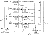
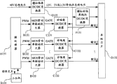
图1是现有技术一的电源架构图;FIG. 1 is a power supply architecture diagram of prior art 1;
图2是现有技术二的电源架构图;FIG. 2 is a power supply architecture diagram of the second prior art;
图3是现有技术的时序控制示意图;FIG. 3 is a schematic diagram of timing control in the prior art;
图4是本发明电源架构原理简图;Fig. 4 is a schematic diagram of the principle of the power architecture of the present invention;
图5是本发明实施例1的电源架构图;FIG. 5 is a power supply architecture diagram of Embodiment 1 of the present invention;
图6是本发明实施例2的电源架构图;FIG. 6 is a power architecture diagram of Embodiment 2 of the present invention;
图7是本发明实施例3的电源架构图;FIG. 7 is a power supply architecture diagram of Embodiment 3 of the present invention;
图8是本发明实施例4的电源架构图;FIG. 8 is a power supply architecture diagram of Embodiment 4 of the present invention;
图9是本发明实施例5的电源架构图;FIG. 9 is a power supply architecture diagram of Embodiment 5 of the present invention;
图10是本发明实施例6的电源架构图;FIG. 10 is a power supply architecture diagram of Embodiment 6 of the present invention;
图11是本发明实施例7的电源架构图;FIG. 11 is a power supply architecture diagram of Embodiment 7 of the present invention;
图12是本发明实施例8的电源架构图;FIG. 12 is a power supply architecture diagram of Embodiment 8 of the present invention;
图13是本发明实施例9的电源架构图。FIG. 13 is a diagram of the power supply structure of Embodiment 9 of the present invention.
具体实施方式 Detailed ways
下面结合附图及具体实施例对本发明详细说明。The present invention will be described in detail below in conjunction with the accompanying drawings and specific embodiments.
本发明所提供的单板电源架构及电源提供方法,均可由运算处理器向DC/DC变换器发送控制电源输出的控制信号,再由DC/DC变换器根据收到的控制信号将收到的总线电压变换为所需要的电源电压输出。并且,运算处理器可以进一步监控所述电源输出并将监控结果上报给相连的上位机;还可以通过控制发送所述控制信号的时间,控制DC/DC变换器变换出的多个电源输出的时序。The single-board power supply architecture and power supply method provided by the present invention can send a control signal to control the output of the power supply by the arithmetic processor to the DC/DC converter, and then the DC/DC converter will receive the received control signal according to the received control signal. The bus voltage is converted to the required power supply voltage output. In addition, the arithmetic processor can further monitor the output of the power supply and report the monitoring result to the connected host computer; it can also control the timing of multiple power outputs converted by the DC/DC converter by controlling the time for sending the control signal .
总体来讲,本发明的核心思想可以由图4体现。图4中,微处理器(A)、MOS管功率驱动放大器(B)、DC/DC变换器(C)和单板芯片(D)依次相连,微处理器(A)还与上位机(E)相连。Generally speaking, the core idea of the present invention can be embodied by FIG. 4 . In Fig. 4, the microprocessor (A), the MOS tube power drive amplifier (B), the DC/DC converter (C) and the single-board chip (D) are connected in sequence, and the microprocessor (A) is also connected with the host computer (E ) connected.
实际应用时,微处理器(A)产生占空比可调的PWM脉冲,该PWM脉冲经过MOS管功率驱动放大器(B)放大后驱动DC/DC变换器(C)将收到的总线电压变换成单板芯片(D)所需要的芯片电压。具体而言,驱动DC/DC变换器(C)以实现电压、电流变换的方式通常为:MOS管功率驱动放大器(B)将放大所述PWM脉冲后所形成的GATE信号发送给DC/DC变换器(C),由该GATE信号触发DC/DC变换器(C)进行电压、电流变换。In actual application, the microprocessor (A) generates a PWM pulse with an adjustable duty ratio, and the PWM pulse is amplified by the MOS transistor power drive amplifier (B) to drive the DC/DC converter (C) to convert the received bus voltage The chip voltage required to form a single-board chip (D). Specifically, the way to drive the DC/DC converter (C) to achieve voltage and current conversion is usually: the MOS transistor power drive amplifier (B) sends the GATE signal formed after amplifying the PWM pulse to the DC/DC converter device (C), and the DC/DC converter (C) is triggered by the GATE signal to perform voltage and current conversion.
再有,微处理器(A)可以监控输出给单板芯片(D)的电压、电流,并将监控结果通过通信接口上报给上位机(E)。当然,微处理器(A)可以通过向MOS管功率驱动放大器(B)发送PWM脉冲,来调整DC/DC变换器(C)所输出的电压、电流。Furthermore, the microprocessor (A) can monitor the voltage and current output to the single board chip (D), and report the monitoring results to the host computer (E) through the communication interface. Of course, the microprocessor (A) can adjust the voltage and current output by the DC/DC converter (C) by sending PWM pulses to the MOS transistor power drive amplifier (B).
下面参照附图详细说明本发明的实施例。Embodiments of the present invention will be described in detail below with reference to the accompanying drawings.
为使实施方式能够清楚明白地体现本发明技术特征,本发明所列举的各实施例所对应的附图中的非隔离DC/DC变换器和MOS管功率驱动放大器的数量一般都是3个;当然,在实际应用中,所述非隔离DC/DC变换器和MOS管功率驱动放大器的数量则不一定必须是三个,也可以是一个或多个。In order to enable the implementation to clearly embody the technical features of the present invention, the number of non-isolated DC/DC converters and MOS tube power drive amplifiers in the drawings corresponding to the various embodiments listed in the present invention is generally three; Of course, in practical applications, the number of the non-isolated DC/DC converter and the MOS tube power driving amplifier does not necessarily have to be three, and may also be one or more.
实施例1:Example 1:
参见图5,图5所示为本发明实施例1的电源架构图。图5中,微处理器A51与单板芯片之间依次连接有多路MOS管功率驱动放大器、非隔离DC/DC变换器;每一路MOS管功率驱动放大器和非隔离DC/DC变换器之间则为串联关系。并且,微处理器A51还可以进一步与上位机E51相连。Referring to FIG. 5 , FIG. 5 is a power architecture diagram of Embodiment 1 of the present invention. In Fig. 5, multiple MOS tube power drive amplifiers and non-isolated DC/DC converters are sequentially connected between the microprocessor A51 and the single-board chip; between each MOS tube power drive amplifier and the non-isolated DC/DC converter is a serial relationship. Moreover, the microprocessor A51 can be further connected with the upper computer E51.
实际应用时,微处理器A51产生占空比可调的PWM脉冲,该PWM脉冲分三路分别经过MOS管功率驱动放大器B51~B53放大后,分别驱动非隔离DC/DC变换器C51~C53将收到的12V、5V或3.3V等低压总线电压变换成单板芯片D51所需要的芯片电压。并且,当单板芯片D51对低压总线电压有需求时,可直接将低压总线电压输入单板芯片D51。具体而言,驱动所述非隔离DC/DC变换器以实现电压、电流变换的方式通常为:MOS管功率驱动放大器将放大所述PWM脉冲后所形成的GATE信号发送给非隔离DC/DC变换器,由该GATE信号触发非隔离DC/DC变换器进行电压、电流变换。In practical applications, the microprocessor A51 generates PWM pulses with adjustable duty ratios. The PWM pulses are divided into three channels and amplified by the MOS transistor power drive amplifiers B51~B53 respectively to drive the non-isolated DC/DC converters C51~C53 respectively. The received low-voltage bus voltage of 12V, 5V or 3.3V is transformed into the chip voltage required by the single-board chip D51. Moreover, when the single-board chip D51 has a demand for the low-voltage bus voltage, the low-voltage bus voltage can be directly input into the single-board chip D51. Specifically, the way to drive the non-isolated DC/DC converter to realize voltage and current conversion is usually: the MOS transistor power drive amplifier sends the GATE signal formed after amplifying the PWM pulse to the non-isolated DC/DC converter The non-isolated DC/DC converter is triggered by the GATE signal to perform voltage and current conversion.
再有,微处理器A51可以以采样等方式监控输出给单板芯片D51的电压、电流,并将采样结果等监控结果通过通信接口周期性或实时性地上报给上位机E51。当然,微处理器A51可以通过向所述MOS管功率驱动放大器发送PWM脉冲,来调整所述非隔离DC/DC变换器所输出的电压、电流。比如:微处理器A51通过监控获知非隔离DC/DC变换器C51所输出的电压偏大,微处理器A51则向MOS管功率驱动放大器B51发送用于降低电压的PWM脉冲;该PWM脉冲经过MOS管功率驱动放大器B51后,驱动非隔离DC/DC变换器C51变换出比之前输出电压相对低的电压。Furthermore, the microprocessor A51 can monitor the voltage and current output to the single-board chip D51 by means of sampling, etc., and report the monitoring results such as sampling results to the host computer E51 periodically or in real time through the communication interface. Of course, the microprocessor A51 can adjust the voltage and current output by the non-isolated DC/DC converter by sending PWM pulses to the MOS transistor power drive amplifier. For example, the microprocessor A51 learns through monitoring that the output voltage of the non-isolated DC/DC converter C51 is too large, and the microprocessor A51 sends a PWM pulse for reducing the voltage to the MOS tube power drive amplifier B51; the PWM pulse passes through the MOS After the tube power drives the amplifier B51, it drives the non-isolated DC/DC converter C51 to convert a voltage that is relatively lower than the previous output voltage.
另外,当输出给单板芯片D51的各电压之间有时序要求时,微处理器A51可通过控制各PWM脉冲输出时间以精确控制各MOS管功率驱动放大器处于导通或截止状态的时间,以此实现对输入单板芯片313的电流的精确时序控制,即:实现单板电源的精确时序控制。In addition, when there is a sequence requirement between the voltages output to the single-board chip D51, the microprocessor A51 can precisely control the time when each MOS tube power drive amplifier is in the on or off state by controlling the output time of each PWM pulse, so as to This realizes precise sequential control of the current input to the single-
实施例2:Example 2:
参见图6,图6所示为本发明实施例2的电源架构图,该电源架构可以以实施例1为基础变换得到。图6与图5的区别在于:在非隔离DC/DC变换器C63与单板芯片D61之间进一步串连有模拟非隔离线性DC/DC变换器F61。模拟非隔离线性DC/DC变换器F61可以对来自非隔离DC/DC变换器C63的电压进行线性变换,最终得到单板芯片D61所需要的电压并输出给单板芯片D61。Referring to FIG. 6 , FIG. 6 shows a diagram of a power supply architecture of Embodiment 2 of the present invention, which can be obtained by transforming the power supply architecture based on Embodiment 1. Referring to FIG. The difference between FIG. 6 and FIG. 5 is that an analog non-isolated linear DC/DC converter F61 is further connected in series between the non-isolated DC/DC converter C63 and the single-board chip D61. The analog non-isolated linear DC/DC converter F61 can linearly convert the voltage from the non-isolated DC/DC converter C63 to finally obtain the voltage required by the single-board chip D61 and output it to the single-board chip D61.
在实际应用中,模拟非隔离线性DC/DC变换器F61可以串连于任意非隔离DC/DC变换器与单板芯片D61之间。所述非隔离DC/DC变换器可以是普通的模拟非隔离DC/DC变换器或模拟非隔离线性DC/DC变换器。In practical applications, the analog non-isolated linear DC/DC converter F61 can be connected in series between any non-isolated DC/DC converter and the single-board chip D61. The non-isolated DC/DC converter may be a common analog non-isolated DC/DC converter or an analog non-isolated linear DC/DC converter.
实施例3:Example 3:
参见图7,图7所示为本发明实施例3的电源架构图,该电源架构可以以实施例1为基础变换得到。图7与图5的区别在于:单板芯片D71进一步与模拟非隔离线性DC/DC变换器F71相连;模拟非隔离线性DC/DC变换器F71可以接收12V、5V或3.3V等低压总线电压,并将收到的总线电压直接变换为单板芯片D71所需要的电压再输出给单板芯片D71。Referring to FIG. 7, FIG. 7 is a diagram of a power supply architecture of Embodiment 3 of the present invention, which can be obtained by transforming the power supply architecture based on Embodiment 1. Referring to FIG. The difference between Fig. 7 and Fig. 5 is that the single-board chip D71 is further connected with the analog non-isolated linear DC/DC converter F71; the analog non-isolated linear DC/DC converter F71 can receive low-voltage bus voltages such as 12V, 5V or 3.3V, The received bus voltage is directly converted into the voltage required by the single-board chip D71 and then output to the single-board chip D71.
实施例4:Example 4:
参见图8,图8所示为本发明实施例4的电源架构图,该电源架构可以以实施例3为基础变换得到。图8与图7的区别在于:在非隔离DC/DC变换器C83与单板芯片D81之间进一步串连有模拟非隔离线性DC/DC变换器F81。模拟非隔离线性DC/DC变换器F81可以对来自非隔离DC/DC变换器C83的电压进行线性变换,最终得到单板芯片D81所需要的电压并输出给单板芯片D81。Referring to FIG. 8 , FIG. 8 is a diagram of a power architecture of Embodiment 4 of the present invention, which can be obtained by transforming the power architecture based on Embodiment 3. The difference between FIG. 8 and FIG. 7 is that an analog non-isolated linear DC/DC converter F81 is further connected in series between the non-isolated DC/DC converter C83 and the single-board chip D81. The analog non-isolated linear DC/DC converter F81 can linearly convert the voltage from the non-isolated DC/DC converter C83, and finally obtain the voltage required by the single-board chip D81 and output it to the single-board chip D81.
在实际应用中,模拟非隔离线性DC/DC变换器F81可以串连于任意非隔离DC/DC变换器与单板芯片D81之间。所述非隔离DC/DC变换器可以是普通的模拟非隔离DC/DC变换器或模拟非隔离线性DC/DC变换器。In practical applications, the analog non-isolated linear DC/DC converter F81 can be connected in series between any non-isolated DC/DC converter and the single-board chip D81. The non-isolated DC/DC converter may be a common analog non-isolated DC/DC converter or an analog non-isolated linear DC/DC converter.
实施例5:Example 5:
参见图9,图9所示为本发明实施例5的电源架构图,该电源架构可以以实施例1为基础变换得到。图9与图5的区别在于:微处理器A91与单板芯片D91之间进一步串联有MOS管功率驱动放大器C104和隔离DC/DC变换器F91,12V、5V或3.3V等低压总线电压是由隔离DC/DC变换器F91变换得到的,该变换方法为:微处理器A91产生占空比可调的PWM脉冲,该PWM脉冲经过MOS管功率驱动放大器C104放大后,驱动隔离DC/DC变换器F91将收到的目前较常用的48V总线电压变换成12V、5V或3.3V等低压总线电压。Referring to FIG. 9 , FIG. 9 is a power supply architecture diagram of Embodiment 5 of the present invention, which can be obtained by transforming the power supply architecture based on Embodiment 1. Referring to FIG. The difference between Fig. 9 and Fig. 5 is that: between the microprocessor A91 and the single-board chip D91, a MOS transistor power drive amplifier C104 and an isolated DC/DC converter F91 are further connected in series, and low-voltage bus voltages such as 12V, 5V or 3.3V are generated by The isolated DC/DC converter F91 is converted. The conversion method is: the microprocessor A91 generates a PWM pulse with an adjustable duty cycle, and the PWM pulse is amplified by the MOS tube power drive amplifier C104 to drive the isolated DC/DC converter. F91 transforms the received 48V bus voltage into low-voltage bus voltages such as 12V, 5V or 3.3V.
实施例6:Embodiment 6:
参见图10,图10所示为本发明实施例6的电源架构图,该电源架构可以以实施例5为基础变换得到。图10与图9的区别在于:与MOS管功率驱动放大器B104串联的不是微处理器A101而是微处理器A102,以便微处理器A102能相对独立地控制隔离DC/DC变换器F101进行电压、电流变换。Referring to FIG. 10 , FIG. 10 is a diagram of a power supply architecture of Embodiment 6 of the present invention, which can be obtained by transforming the power supply architecture based on Embodiment 5. Referring to FIG. The difference between Fig. 10 and Fig. 9 is that the microprocessor A102 is not the microprocessor A101 connected in series with the MOS transistor power drive amplifier B104, so that the microprocessor A102 can relatively independently control the isolated DC/DC converter F101 for voltage, current conversion.
实施例7:Embodiment 7:
参见图11,图11所示为本发明实施例7的电源架构图,该电源架构可以以实施例1为基础变换得到。图11与图5的区别在于:单板芯片D111进一步与模拟隔离DC/DC变换器G111相连,12V、5V或3.3V等低压总线电压是由模拟隔离DC/DC变换器G111变换得到的,该变换方法为:模拟隔离DC/DC变换器G111将收到的目前较常用的48V总线电压变换成12V、5V或3.3V等低压总线电压。Referring to FIG. 11 , FIG. 11 is a diagram of a power supply architecture of Embodiment 7 of the present invention, which can be obtained by transforming the power supply architecture based on Embodiment 1. The difference between Figure 11 and Figure 5 is that the single-board chip D111 is further connected to the analog isolated DC/DC converter G111, and the low-voltage bus voltage such as 12V, 5V or 3.3V is converted by the analog isolated DC/DC converter G111. The conversion method is as follows: the analog isolation DC/DC converter G111 converts the currently received 48V bus voltage into a low-voltage bus voltage such as 12V, 5V or 3.3V.
实施例8:Embodiment 8:
参见图12,图12所示为本发明实施例8的电源架构图,该电源架构可以以实施例7为基础变换得到。图12与图11的区别在于:在非隔离DC/DC变换器C123与单板芯片D121之间进一步串连有模拟非隔离线性DC/DC变换器F121。模拟非隔离线性DC/DC变换器F121可以对来自非隔离DC/DC变换器C123的电压进行线性变换,最终得到单板芯片D121所需要的电压并输出给单板芯片D121。Referring to FIG. 12 , FIG. 12 is a power supply architecture diagram of Embodiment 8 of the present invention, which can be obtained by transforming the power supply architecture based on Embodiment 7. The difference between FIG. 12 and FIG. 11 is that an analog non-isolated linear DC/DC converter F121 is further connected in series between the non-isolated DC/DC converter C123 and the single-board chip D121. The analog non-isolated linear DC/DC converter F121 can linearly convert the voltage from the non-isolated DC/DC converter C123 to finally obtain the voltage required by the single-board chip D121 and output it to the single-board chip D121.
在实际应用中,模拟非隔离线性DC/DC变换器F121可以串连于任意非隔离DC/DC变换器与单板芯片D121之间。所述非隔离DC/DC变换器可以是普通的模拟非隔离DC/DC变换器或模拟非隔离线性DC/DC变换器。In practical applications, the analog non-isolated linear DC/DC converter F121 can be connected in series between any non-isolated DC/DC converter and the single-board chip D121. The non-isolated DC/DC converter may be a common analog non-isolated DC/DC converter or an analog non-isolated linear DC/DC converter.
实施例9:Embodiment 9:
参见图13,图13所示为本发明实施例9的电源架构图,该电源架构可以以实施例7为基础变换得到。图13与图11的区别在于:单板芯片D131进一步与模拟非隔离线性DC/DC变换器F131相连;模拟非隔离线性DC/DC变换器F131可以接收12V、5V或3.3V等低压总线电压,并将收到的总线电压直接变换为单板芯片D131所需要的电压再输出给单板芯片D131。Referring to FIG. 13 , FIG. 13 is a diagram of a power supply architecture of Embodiment 9 of the present invention, which can be obtained by transforming the power supply architecture based on Embodiment 7. The difference between Fig. 13 and Fig. 11 is that the single-board chip D131 is further connected with the analog non-isolated linear DC/DC converter F131; the analog non-isolated linear DC/DC converter F131 can receive low-voltage bus voltages such as 12V, 5V or 3.3V, And the received bus voltage is directly converted into the voltage required by the single-board chip D131 and then output to the single-board chip D131.
在实际应用中,所述非隔离DC/DC变换器可以包含模拟非隔离DC/DC变换器或者数字非隔离DC/DC变换器;所述MOS管功率驱动放大器则可以包含推挽功率驱动放大方式或集成功率驱动放大方式。再有,所述非隔离DC/DC变换器可以包含能够实现升压的升压DC/DC变换器,也可以包含能够实现降压的非隔离降压DC/DC变换器;同理,所述隔离DC/DC变换器可以包含能够实现升压的隔离升压DC/DC变换器,也可以包含能够实现降压的隔离降压DC/DC变换器。In practical applications, the non-isolated DC/DC converter may include an analog non-isolated DC/DC converter or a digital non-isolated DC/DC converter; the MOS transistor power drive amplifier may include a push-pull power drive amplification method Or integrated power drive amplification. Furthermore, the non-isolated DC/DC converter may include a step-up DC/DC converter capable of boosting, or may include a non-isolated step-down DC/DC converter capable of stepping down; similarly, the The isolated DC/DC converter may include an isolated step-up DC/DC converter capable of boosting voltage, or may include an isolated step-down DC/DC converter capable of stepping down.
还有,在实际应用时,也可以应用其它的功率驱动放大器,而不应用MOS管功率驱动放大器;并且,如果微处理器输出的PWM脉冲所具有的功率足够大,以至于可以正常触发非隔离DC/DC变换器等DC/DC变换器进行电压、电流变换,那么也可以去掉所述MOS管功率驱动放大器,而使微处理器与DC/DC变换器直接相连,由微处理器所输出的PWM脉冲直接控制DC/DC变换器进行电压、电流变换。再有,所述的微处理器可以是单片机、数字信号处理器(DSP)、复杂可编程逻辑器件(CPLD)、现场可编程逻辑门阵列(FPGA)等运算处理器。Also, in practical applications, other power drive amplifiers can be used instead of MOS tube power drive amplifiers; and, if the power of the PWM pulse output by the microprocessor is large enough, it can normally trigger the non-isolated DC/DC converters such as DC/DC converters perform voltage and current conversion, so the MOS tube power drive amplifier can also be removed, and the microprocessor is directly connected with the DC/DC converter, and the output output by the microprocessor The PWM pulse directly controls the DC/DC converter for voltage and current conversion. Furthermore, the microprocessor may be an arithmetic processor such as a single-chip microcomputer, a digital signal processor (DSP), a complex programmable logic device (CPLD), and a field programmable logic gate array (FPGA).
本发明所提供的单板电源架构及电源提供方法也可以应用于除通信领域以外的其它技术领域,只要本发明单板电源架构及电源提供方法能统一、及时、有效地监控作为单板电源输出的电压、电流即可。The single-board power supply architecture and power supply method provided by the present invention can also be applied to other technical fields other than the communication field, as long as the single-board power supply architecture and power supply method of the present invention can uniformly, timely and effectively monitor the single-board power supply output voltage and current.
由以上所述可见,本发明提供的单板电源架构及电源提供方法,在不出现多种类型并且无法统一管理的模拟变换器、以及不需要应用专业的时序控制芯片额外进行复杂时序控制的情况下,可由微处理器实现统一、及时、有效地单板电源监控,并可进一步由微处理器实现单板电源的精确时序控制。It can be seen from the above that the single-board power supply architecture and power supply method provided by the present invention do not have multiple types of analog converters that cannot be managed uniformly, and do not require the application of professional timing control chips for additional complex timing control. Under this condition, the unified, timely and effective single-board power supply monitoring can be realized by the microprocessor, and the precise timing control of the single-board power supply can be further realized by the microprocessor.
Claims (15)
Priority Applications (6)
| Application Number | Priority Date | Filing Date | Title |
|---|---|---|---|
| CNB2006100810254A CN100426193C (en) | 2006-05-19 | 2006-05-19 | Single-board power construction and power supply |
| EP18170972.6A EP3487054A1 (en) | 2006-05-19 | 2007-03-12 | Single-board power supply structure and method for providing power supply |
| ES07711077.3T ES2687248T3 (en) | 2006-05-19 | 2007-03-12 | Single plate power supply and method to provide power supply |
| PCT/CN2007/000789 WO2007134510A1 (en) | 2006-05-19 | 2007-03-12 | A single-desk power supply and a method for providing a power supply |
| EP07711077.3A EP2019479B1 (en) | 2006-05-19 | 2007-03-12 | A single-desk power supply and a method for providing a power supply |
| US12/246,867 US7847528B2 (en) | 2006-05-19 | 2008-10-07 | Single-board power supply structure and method for providing power supply |
Applications Claiming Priority (1)
| Application Number | Priority Date | Filing Date | Title |
|---|---|---|---|
| CNB2006100810254A CN100426193C (en) | 2006-05-19 | 2006-05-19 | Single-board power construction and power supply |
Publications (2)
| Publication Number | Publication Date |
|---|---|
| CN1983117A CN1983117A (en) | 2007-06-20 |
| CN100426193C true CN100426193C (en) | 2008-10-15 |
Family
ID=38165695
Family Applications (1)
| Application Number | Title | Priority Date | Filing Date |
|---|---|---|---|
| CNB2006100810254A Active CN100426193C (en) | 2006-05-19 | 2006-05-19 | Single-board power construction and power supply |
Country Status (5)
| Country | Link |
|---|---|
| US (1) | US7847528B2 (en) |
| EP (2) | EP2019479B1 (en) |
| CN (1) | CN100426193C (en) |
| ES (1) | ES2687248T3 (en) |
| WO (1) | WO2007134510A1 (en) |
Cited By (2)
| Publication number | Priority date | Publication date | Assignee | Title |
|---|---|---|---|---|
| US7847528B2 (en) | 2006-05-19 | 2010-12-07 | Huawei Technologies Co., Ltd. | Single-board power supply structure and method for providing power supply |
| CN102916574A (en) * | 2011-08-02 | 2013-02-06 | 伊博电源(杭州)有限公司 | Power supply control system |
Families Citing this family (12)
| Publication number | Priority date | Publication date | Assignee | Title |
|---|---|---|---|---|
| CN101567624B (en) * | 2008-04-21 | 2011-12-21 | 华为技术有限公司 | Control circuit for switching power supply voltage, control method, power supply module and veneer |
| US8193864B2 (en) * | 2009-05-14 | 2012-06-05 | Lineage Power Corporation | High efficiency power amplifier power architecture |
| US8400791B2 (en) | 2010-07-16 | 2013-03-19 | Rockwell Automation Technologies, Inc. | Power layer generation of inverter gate drive signals |
| US8817933B2 (en) | 2013-01-09 | 2014-08-26 | Rockwell Automation Technologies, Inc. | Method and apparatus for clock data recovery from Manchester coded serial data stream |
| CN104571254B (en) * | 2013-10-14 | 2016-06-15 | 技嘉科技股份有限公司 | Apparatus and method for power output stage control system applied to high-speed bus device |
| CN104065268B (en) * | 2014-06-17 | 2017-12-05 | 华为技术有限公司 | Supply network on a kind of piece |
| CN104104434A (en) * | 2014-07-24 | 2014-10-15 | 北京华环电子股份有限公司 | Power failure alarm implementation method capable of rapidly inserting alarm frame |
| CN104460930B (en) * | 2014-12-31 | 2017-06-13 | 广东威创视讯科技股份有限公司 | ATX reference power supplies realize device |
| US10447276B2 (en) * | 2015-10-27 | 2019-10-15 | Andapt, Inc. | Power management integrated circuit integrating field effect transistors and programmable fabric |
| CN108900086B (en) * | 2018-08-01 | 2020-01-17 | 环鸿电子(昆山)有限公司 | Programmable isolated power circuit structure and system |
| CN110401328B (en) * | 2019-05-14 | 2020-11-24 | 无锡海斯凯尔医学技术有限公司 | Power supply and system |
| CN110196613B (en) * | 2019-05-28 | 2021-03-30 | 电子科技大学 | Power supply device for DUT in integrated circuit test system |
Citations (4)
| Publication number | Priority date | Publication date | Assignee | Title |
|---|---|---|---|---|
| JP2000295769A (en) * | 1999-04-07 | 2000-10-20 | Nec Corp | Circuit for reducing power consumption of logical circuit, and method of reducing power consumption used for it |
| CN1472863A (en) * | 2002-08-02 | 2004-02-04 | 华为技术有限公司 | Single board power supply backup method and single board power supply backup system |
| US20040217651A1 (en) * | 2003-05-02 | 2004-11-04 | Brown David Alan | Sequencing power supplies on daughter boards |
| US6879139B2 (en) * | 2003-05-02 | 2005-04-12 | Potentia Semiconductor, Inc. | Sequencing power supplies |
Family Cites Families (14)
| Publication number | Priority date | Publication date | Assignee | Title |
|---|---|---|---|---|
| US4797833A (en) * | 1986-09-30 | 1989-01-10 | Louisiana State University | Microprocessor based controller for a three phase bridge rectifier |
| DE4424800A1 (en) * | 1994-07-14 | 1996-01-18 | Philips Patentverwaltung | Circuit arrangement for supplying supply voltages |
| US5835350A (en) * | 1996-12-23 | 1998-11-10 | Lucent Technologies Inc. | Encapsulated, board-mountable power supply and method of manufacture therefor |
| EP1032964A2 (en) * | 1997-11-17 | 2000-09-06 | Lifestyle Technologies | Universal power supply |
| AU2002211583A1 (en) * | 2000-10-10 | 2002-04-22 | Primarion, Inc. | System and method for highly phased power regulation |
| US6809678B2 (en) * | 2002-10-16 | 2004-10-26 | Perkinelmer Inc. | Data processor controlled DC to DC converter system and method of operation |
| US7187562B2 (en) * | 2002-11-11 | 2007-03-06 | International Rectifier Corporation | Two stage power conversion circuit |
| US7456617B2 (en) | 2002-11-13 | 2008-11-25 | Power-One, Inc. | System for controlling and monitoring an array of point-of-load regulators by a host |
| US6771052B2 (en) * | 2003-01-03 | 2004-08-03 | Astec International Limited | Programmable multiple output DC-DC isolated power supply |
| US6936999B2 (en) * | 2003-03-14 | 2005-08-30 | Power-One Limited | System and method for controlling output-timing parameters of power converters |
| CN2655309Y (en) * | 2003-07-16 | 2004-11-10 | 华为技术有限公司 | Power supply time sequence controlling circuit |
| CN2639935Y (en) * | 2003-09-03 | 2004-09-08 | 上海安伏激光电子电气设备有限公司 | Programmable controller controlling circuit for electro-static dust removal constant current high voltage direct current power source |
| US7019505B2 (en) * | 2004-01-29 | 2006-03-28 | Enpirion, Inc. | Digital controller for a power converter employing selectable phases of a clock signal |
| CN100426193C (en) | 2006-05-19 | 2008-10-15 | 华为技术有限公司 | Single-board power construction and power supply |
-
2006
- 2006-05-19 CN CNB2006100810254A patent/CN100426193C/en active Active
-
2007
- 2007-03-12 EP EP07711077.3A patent/EP2019479B1/en active Active
- 2007-03-12 ES ES07711077.3T patent/ES2687248T3/en active Active
- 2007-03-12 EP EP18170972.6A patent/EP3487054A1/en active Pending
- 2007-03-12 WO PCT/CN2007/000789 patent/WO2007134510A1/en not_active Ceased
-
2008
- 2008-10-07 US US12/246,867 patent/US7847528B2/en active Active
Patent Citations (4)
| Publication number | Priority date | Publication date | Assignee | Title |
|---|---|---|---|---|
| JP2000295769A (en) * | 1999-04-07 | 2000-10-20 | Nec Corp | Circuit for reducing power consumption of logical circuit, and method of reducing power consumption used for it |
| CN1472863A (en) * | 2002-08-02 | 2004-02-04 | 华为技术有限公司 | Single board power supply backup method and single board power supply backup system |
| US20040217651A1 (en) * | 2003-05-02 | 2004-11-04 | Brown David Alan | Sequencing power supplies on daughter boards |
| US6879139B2 (en) * | 2003-05-02 | 2005-04-12 | Potentia Semiconductor, Inc. | Sequencing power supplies |
Non-Patent Citations (6)
| Title |
|---|
| Distributed Power Architecture Demand Characteristics. Linnea Brush.IEEE. 2004 |
| Distributed Power Architecture Demand Characteristics. Linnea Brush.IEEE. 2004 * |
| Distributed Power Systems. Bob Mammano.UNITRODE CORPORATION. 1993 |
| Distributed Power Systems. Bob Mammano.UNITRODE CORPORATION. 1993 * |
| 分布式通信电源技术的发展. 郭永香,郭宇明.仪器仪表用户,第11卷第1期. 2004 |
| 分布式通信电源技术的发展. 郭永香,郭宇明.仪器仪表用户,第11卷第1期. 2004 * |
Cited By (3)
| Publication number | Priority date | Publication date | Assignee | Title |
|---|---|---|---|---|
| US7847528B2 (en) | 2006-05-19 | 2010-12-07 | Huawei Technologies Co., Ltd. | Single-board power supply structure and method for providing power supply |
| CN102916574A (en) * | 2011-08-02 | 2013-02-06 | 伊博电源(杭州)有限公司 | Power supply control system |
| CN102916574B (en) * | 2011-08-02 | 2016-01-20 | 伊博电源(杭州)有限公司 | A kind of power control system |
Also Published As
| Publication number | Publication date |
|---|---|
| CN1983117A (en) | 2007-06-20 |
| EP2019479B1 (en) | 2018-07-04 |
| US20090033297A1 (en) | 2009-02-05 |
| EP2019479A4 (en) | 2011-07-06 |
| US7847528B2 (en) | 2010-12-07 |
| EP2019479A1 (en) | 2009-01-28 |
| ES2687248T3 (en) | 2018-10-24 |
| WO2007134510A1 (en) | 2007-11-29 |
| EP3487054A1 (en) | 2019-05-22 |
Similar Documents
| Publication | Publication Date | Title |
|---|---|---|
| EP2019479A1 (en) | A single-desk power supply and a method for providing a power supply | |
| JP6367337B2 (en) | Multi-output boost regulator with single control loop | |
| EP2852257B1 (en) | Digital current equalizing device, analog current equalizing device, current equalizing method and system | |
| CN102447393B (en) | There is the regulated power supply system of high input voltage dynamic range | |
| CN100570980C (en) | A wide range energy feedback method and realization circuit of multi-output switching power supply | |
| EP3417542B1 (en) | Switching amplifiers and power converters | |
| CN103053102A (en) | Ripple Current Reduction Using Bridge Topology In Switching Mode Power Converters | |
| CN102638179A (en) | Efficiency optimized power converter with dual voltage power factor correction | |
| CN108463942A (en) | Multiple input/multiple output dc-dc converter | |
| CN103187753A (en) | Charging power supply current-sharing control system and method of parallel three-path output | |
| CN101507090B (en) | Multiple output multiple topology voltage converter | |
| CN102474183A (en) | Power supply with dynamic input current suppression | |
| EP1879284A3 (en) | DC-DC converter and power supply apparatus | |
| US8269461B2 (en) | Hybrid battery charger and control circuit and method thereof | |
| CN105612683A (en) | Voltage regulator with charge pump for generating second voltage source | |
| WO2022161184A1 (en) | Power source module and power source system | |
| CN106208688B (en) | Switching power converter and control method thereof | |
| CN203984025U (en) | Make battery-powered device | |
| CN101989755B (en) | Hybrid charger and its control circuit and method | |
| CN110391686A (en) | Charge-discharge control circuit | |
| CN109802568A (en) | A kind of wide range output power inverter of varistructure and parameter self-tuning | |
| CN102916574B (en) | A kind of power control system | |
| CN201312260Y (en) | Digital power circuit and digital power provided with the circuit | |
| CN100367642C (en) | Method for improving transient noise of switching DC-DC converter with multiple output voltages | |
| CN220605894U (en) | Pulse power supply generator |
Legal Events
| Date | Code | Title | Description |
|---|---|---|---|
| C06 | Publication | ||
| PB01 | Publication | ||
| C10 | Entry into substantive examination | ||
| SE01 | Entry into force of request for substantive examination | ||
| C14 | Grant of patent or utility model | ||
| GR01 | Patent grant |