CN100433112C - Apparatus and method for driving liquid crystal display - Google Patents
Apparatus and method for driving liquid crystal display Download PDFInfo
- Publication number
- CN100433112C CN100433112C CNB021586691A CN02158669A CN100433112C CN 100433112 C CN100433112 C CN 100433112C CN B021586691 A CNB021586691 A CN B021586691A CN 02158669 A CN02158669 A CN 02158669A CN 100433112 C CN100433112 C CN 100433112C
- Authority
- CN
- China
- Prior art keywords
- voltage
- liquid crystal
- data signal
- normal driving
- real data
- Prior art date
- Legal status (The legal status is an assumption and is not a legal conclusion. Google has not performed a legal analysis and makes no representation as to the accuracy of the status listed.)
- Expired - Fee Related
Links
Images




Classifications
-
- G—PHYSICS
- G09—EDUCATION; CRYPTOGRAPHY; DISPLAY; ADVERTISING; SEALS
- G09G—ARRANGEMENTS OR CIRCUITS FOR CONTROL OF INDICATING DEVICES USING STATIC MEANS TO PRESENT VARIABLE INFORMATION
- G09G3/00—Control arrangements or circuits, of interest only in connection with visual indicators other than cathode-ray tubes
- G09G3/20—Control arrangements or circuits, of interest only in connection with visual indicators other than cathode-ray tubes for presentation of an assembly of a number of characters, e.g. a page, by composing the assembly by combination of individual elements arranged in a matrix no fixed position being assigned to or needed to be assigned to the individual characters or partial characters
- G09G3/34—Control arrangements or circuits, of interest only in connection with visual indicators other than cathode-ray tubes for presentation of an assembly of a number of characters, e.g. a page, by composing the assembly by combination of individual elements arranged in a matrix no fixed position being assigned to or needed to be assigned to the individual characters or partial characters by control of light from an independent source
- G09G3/36—Control arrangements or circuits, of interest only in connection with visual indicators other than cathode-ray tubes for presentation of an assembly of a number of characters, e.g. a page, by composing the assembly by combination of individual elements arranged in a matrix no fixed position being assigned to or needed to be assigned to the individual characters or partial characters by control of light from an independent source using liquid crystals
-
- G—PHYSICS
- G09—EDUCATION; CRYPTOGRAPHY; DISPLAY; ADVERTISING; SEALS
- G09G—ARRANGEMENTS OR CIRCUITS FOR CONTROL OF INDICATING DEVICES USING STATIC MEANS TO PRESENT VARIABLE INFORMATION
- G09G3/00—Control arrangements or circuits, of interest only in connection with visual indicators other than cathode-ray tubes
- G09G3/20—Control arrangements or circuits, of interest only in connection with visual indicators other than cathode-ray tubes for presentation of an assembly of a number of characters, e.g. a page, by composing the assembly by combination of individual elements arranged in a matrix no fixed position being assigned to or needed to be assigned to the individual characters or partial characters
- G09G3/34—Control arrangements or circuits, of interest only in connection with visual indicators other than cathode-ray tubes for presentation of an assembly of a number of characters, e.g. a page, by composing the assembly by combination of individual elements arranged in a matrix no fixed position being assigned to or needed to be assigned to the individual characters or partial characters by control of light from an independent source
- G09G3/36—Control arrangements or circuits, of interest only in connection with visual indicators other than cathode-ray tubes for presentation of an assembly of a number of characters, e.g. a page, by composing the assembly by combination of individual elements arranged in a matrix no fixed position being assigned to or needed to be assigned to the individual characters or partial characters by control of light from an independent source using liquid crystals
- G09G3/3611—Control of matrices with row and column drivers
- G09G3/3648—Control of matrices with row and column drivers using an active matrix
-
- G—PHYSICS
- G02—OPTICS
- G02F—OPTICAL DEVICES OR ARRANGEMENTS FOR THE CONTROL OF LIGHT BY MODIFICATION OF THE OPTICAL PROPERTIES OF THE MEDIA OF THE ELEMENTS INVOLVED THEREIN; NON-LINEAR OPTICS; FREQUENCY-CHANGING OF LIGHT; OPTICAL LOGIC ELEMENTS; OPTICAL ANALOGUE/DIGITAL CONVERTERS
- G02F1/00—Devices or arrangements for the control of the intensity, colour, phase, polarisation or direction of light arriving from an independent light source, e.g. switching, gating or modulating; Non-linear optics
- G02F1/01—Devices or arrangements for the control of the intensity, colour, phase, polarisation or direction of light arriving from an independent light source, e.g. switching, gating or modulating; Non-linear optics for the control of the intensity, phase, polarisation or colour
- G02F1/13—Devices or arrangements for the control of the intensity, colour, phase, polarisation or direction of light arriving from an independent light source, e.g. switching, gating or modulating; Non-linear optics for the control of the intensity, phase, polarisation or colour based on liquid crystals, e.g. single liquid crystal display cells
- G02F1/137—Devices or arrangements for the control of the intensity, colour, phase, polarisation or direction of light arriving from an independent light source, e.g. switching, gating or modulating; Non-linear optics for the control of the intensity, phase, polarisation or colour based on liquid crystals, e.g. single liquid crystal display cells characterised by the electro-optical or magneto-optical effect, e.g. field-induced phase transition, orientation effect, guest-host interaction or dynamic scattering
- G02F1/139—Devices or arrangements for the control of the intensity, colour, phase, polarisation or direction of light arriving from an independent light source, e.g. switching, gating or modulating; Non-linear optics for the control of the intensity, phase, polarisation or colour based on liquid crystals, e.g. single liquid crystal display cells characterised by the electro-optical or magneto-optical effect, e.g. field-induced phase transition, orientation effect, guest-host interaction or dynamic scattering based on orientation effects in which the liquid crystal remains transparent
- G02F1/1393—Devices or arrangements for the control of the intensity, colour, phase, polarisation or direction of light arriving from an independent light source, e.g. switching, gating or modulating; Non-linear optics for the control of the intensity, phase, polarisation or colour based on liquid crystals, e.g. single liquid crystal display cells characterised by the electro-optical or magneto-optical effect, e.g. field-induced phase transition, orientation effect, guest-host interaction or dynamic scattering based on orientation effects in which the liquid crystal remains transparent the birefringence of the liquid crystal being electrically controlled, e.g. ECB-, DAP-, HAN-, PI-LC cells
- G02F1/1395—Optically compensated birefringence [OCB]- cells or PI- cells
-
- G—PHYSICS
- G09—EDUCATION; CRYPTOGRAPHY; DISPLAY; ADVERTISING; SEALS
- G09G—ARRANGEMENTS OR CIRCUITS FOR CONTROL OF INDICATING DEVICES USING STATIC MEANS TO PRESENT VARIABLE INFORMATION
- G09G2300/00—Aspects of the constitution of display devices
- G09G2300/04—Structural and physical details of display devices
- G09G2300/0469—Details of the physics of pixel operation
- G09G2300/0478—Details of the physics of pixel operation related to liquid crystal pixels
- G09G2300/0491—Use of a bi-refringent liquid crystal, optically controlled bi-refringence [OCB] with bend and splay states, or electrically controlled bi-refringence [ECB] for controlling the color
-
- G—PHYSICS
- G09—EDUCATION; CRYPTOGRAPHY; DISPLAY; ADVERTISING; SEALS
- G09G—ARRANGEMENTS OR CIRCUITS FOR CONTROL OF INDICATING DEVICES USING STATIC MEANS TO PRESENT VARIABLE INFORMATION
- G09G2320/00—Control of display operating conditions
- G09G2320/02—Improving the quality of display appearance
- G09G2320/0271—Adjustment of the gradation levels within the range of the gradation scale, e.g. by redistribution or clipping
- G09G2320/0276—Adjustment of the gradation levels within the range of the gradation scale, e.g. by redistribution or clipping for the purpose of adaptation to the characteristics of a display device, i.e. gamma correction
-
- G—PHYSICS
- G09—EDUCATION; CRYPTOGRAPHY; DISPLAY; ADVERTISING; SEALS
- G09G—ARRANGEMENTS OR CIRCUITS FOR CONTROL OF INDICATING DEVICES USING STATIC MEANS TO PRESENT VARIABLE INFORMATION
- G09G2330/00—Aspects of power supply; Aspects of display protection and defect management
- G09G2330/02—Details of power systems and of start or stop of display operation
- G09G2330/026—Arrangements or methods related to booting a display
Landscapes
- Engineering & Computer Science (AREA)
- Chemical & Material Sciences (AREA)
- Crystallography & Structural Chemistry (AREA)
- Physics & Mathematics (AREA)
- Computer Hardware Design (AREA)
- General Physics & Mathematics (AREA)
- Theoretical Computer Science (AREA)
- Liquid Crystal Display Device Control (AREA)
- Control Of Indicators Other Than Cathode Ray Tubes (AREA)
- Liquid Crystal (AREA)
Abstract
一种用于驱动液晶显示器的设备,包括一个复位时段之后的一个正常驱动间隔,该正常驱动间隔用于为液晶显示器的正常驱动提供一个真实数据信号,其中液晶显示器包括位于像素电极与公共电极之间的液晶,该液晶在像素电极与公共电极之间一个大于转换电压的电压差上被从张开状态转换成弯曲状态。该设备包括:一个复位电路,用于在复位时段中,在像素电极和公共电极之间设定一个电压差,该电压差大于所述正常驱动间隔中的真实数据信号的平均电压;以及一个控制器,用于对提供给像素电极和公共电极中至少一个的电压进行控制。
A device for driving a liquid crystal display, comprising a normal driving interval after a reset period for providing a real data signal for normal driving of the liquid crystal display, wherein the liquid crystal display includes an electrode located between a pixel electrode and a common electrode The liquid crystal between the pixel electrode and the common electrode is switched from the open state to the curved state at a voltage difference greater than the switching voltage between the pixel electrode and the common electrode. The device includes: a reset circuit for setting a voltage difference between the pixel electrode and the common electrode during the reset period, the voltage difference being greater than the average voltage of the real data signal in the normal driving interval; and a control device for controlling the voltage supplied to at least one of the pixel electrode and the common electrode.
Description
技术领域 technical field
本发明涉及一种用于驱动液晶显示器的技术,尤其涉及一种用于驱动液晶显示器的设备和方法,其中液晶可以从一种张开状态(splaystate)快速转换成一种弯曲状态(bend state)。The present invention relates to a technology for driving a liquid crystal display, and more particularly to an apparatus and method for driving a liquid crystal display, wherein the liquid crystal can be rapidly converted from a splay state to a bend state.
背景技术 Background technique
通常,液晶显示器(LCD)板响应于视频信号而对每个液晶单元的透光率进行控制,由此显示图像。有源矩阵类型的液晶显示板包括用于每个液晶单元的开关装置,由此使每个单元都能更加真实的适于活动图像。在有源矩阵LCD显示器中,薄膜晶体管(TFT)主要用作开关装置。由于这种LCD板可以生产出尺寸比现有阴极射线管显示器更小的设备,因此LCD板已被广泛用作个人计算机或笔记本计算机中的监视器,还被用在复印机等办公室自动化设备以及蜂窝电话或传呼机等便携设备中。Generally, a liquid crystal display (LCD) panel controls light transmittance of each liquid crystal cell in response to a video signal, thereby displaying an image. Liquid crystal display panels of the active matrix type include switching means for each liquid crystal cell, thereby enabling each cell to be more realistically adapted to a moving image. In active matrix LCD displays, thin film transistors (TFTs) are mainly used as switching devices. Because this LCD panel can produce devices smaller in size than existing cathode ray tube displays, LCD panels have been widely used as monitors in personal computers or notebook computers, as well as in office automation equipment such as copiers and cellular in portable devices such as telephones or pagers.
如图1所示,传统的LCD板包括一个将模拟视频信号转换成数字视频数据的数字视频卡30,一个用于提供驱动电压的电源42,一个将视频数据提供给LCD板40的数据线DL的数据驱动器36,一个用于顺序地驱动LCD板40的选通线GL的选通驱动器34,一个控制数据驱动器36和选通驱动器34的控制器32,以及一个γ电压产生器38,用于向数据驱动器36施加一个γ电压。As shown in Figure 1, a conventional LCD panel includes a
在图1所示LCD板40中,液晶(未示出)被注入两个玻璃基板(未示出)之间。选通线GL和数据线DL以相互垂直这样一种方式形成于下玻璃基板之上。在邻近各个选通线GL与数据线DL之间交点的区域都放置了一个薄膜晶体管(TFT),用于有选择的把数据线DL输入的图像数据施加到液晶单元上。为此目的,TFT具有一个连接到选通线GL的栅极端(未示出)和一个连接到数据线DL的源极端(未示出)。TFT的漏极端(未示出)被连接到液晶单元的一个像素电极PIXE。In the
数字视频卡30将模拟图像信号转换成适于LCD板40的数字图像信号,并对包含在模拟图像信号中的同步信号进行检测。控制器32从数字视频卡30接收一个电压范围在0~3.3V,用于表示数字图像信号的驱动电压。控制器32把红、绿、蓝色数字视频数据提供给数据驱动器36。此外,控制器32还使用数字视频卡30输入的水平/垂直同步信号H和V来产生一个点时钟Dclk和一个选通启动脉冲GSP,以便提供对数据驱动器36和选通驱动器34的定时控制。具体地说,点时钟Dclk被提供给数据驱动器36,而选通启动脉冲GSP则被提供给选通驱动器34。The
电源42接收一个来自数字视频卡30,范围在0~3.3V的低电平公共电压,用以产生一个驱动液晶单元的高电平公共电压VDD和一个驱动选通驱动器34的驱动电压。此外,电源42还将所供应的0~3.3V的低电平公共电压VCC转换成15V的高电平公共电压,并把它提供给数据驱动器36。另外,电源42将所供应的0~3.3V的低电平公共电压VCC转换成一个20V的选通高电压VGH和一个-5V的选通低电压VGL,并把它们施加到选通驱动器34上,用于一个与选通扫描时钟GSC相一致的扫描信号。经由液晶显示板的焊盘部分上提供的一个银点,一个7V的公共电压Vcom被作为公共电压提供给液晶显示板的上基板上的公共电极COME。The
选通驱动器34包括:一个移位寄存器,用于响应控制器32输入的选通启动脉冲GSP,以便顺序产生一个扫描脉冲;以及一个电平移动器,用于将扫描脉冲的电压变换成适于驱动液晶单元的电压电平。选通驱动器34把一个选通高电压VGH和一个选通低电压VGL通过选通线GL施加到液晶显示板40上。一个具有选通高电压VGH的扫描脉冲导通TFT,并在TFT导通的一个时间间隔中,将来自数据驱动器36的视频数据切换至液晶单元。The
来自控制器32的点时钟Dclk与红、绿、蓝色数字视频数据一起被输入数据驱动器36。数据驱动器36与点时钟Dclk同步地锁存红、绿、蓝色数字视频数据,然后根据γ电压Vγ来对锁存数据进行校正。此外,数据驱动器36还把经过γ电压Vγ校正的各个红、绿、蓝色数字数据转换成相应的红、绿、蓝色模拟数据,以便应用于LCD板40的数据线DL。The dot clock Dclk from the
对LCD板来说,在液晶中通常使用的是一种扭转向列(TN)模式。在TN模式中,液晶排列的扭转角度是90°,液晶排列状态是根据电场的施加而被改变的,从而控制来自背后照明单元并且穿过液晶的光的透射量。通过使用电场来控制液晶扭曲,透射光数量可以沿灰度级而被改变。然而,将TN模式用于液晶会存在视角狭窄和响应速度慢的问题。For LCD panels, a twisted nematic (TN) mode is commonly used in liquid crystals. In the TN mode, the twist angle of the liquid crystal alignment is 90°, and the liquid crystal alignment state is changed according to the application of an electric field, thereby controlling the amount of light transmitted from the backlight unit and passing through the liquid crystal. By using an electric field to control the liquid crystal twist, the amount of transmitted light can be varied along the gray scale. However, using the TN mode for liquid crystals has problems of narrow viewing angle and slow response speed.
为了克服TN模式的这些缺点,已经建议将液晶与面内切换(IPS)模式或光学补偿弯曲(OCB)模式一起使用。上述模式中的OCB模式具有比TN模式更宽的视角和更快的响应速度。In order to overcome these disadvantages of the TN mode, liquid crystals have been proposed to be used with an in-plane switching (IPS) mode or an optically compensated bend (OCB) mode. The OCB mode among the above modes has a wider viewing angle and faster response speed than the TN mode.
参考图2和图3,OCB模式的LCD板包括:一个上基板10,它顺序地具有一个彩色滤光片阵列(未示出)和一个排列膜(未示出);一个下基板12,它具有一个TFT阵列(未示出)和一个排列膜(未示出);液晶18,它被注入到由一个间隔物(未示出)所确定的上基板10和下基板12之间的一个预期间隙中;分别布置在上、下基板10和12外部的上、下偏光板14和22;一个设置在上基板10和上偏光器14之间的上补偿膜16;以及一个设置在下基板12和下偏光器22之间的补偿膜20,用以补偿入射光相位,从而增加视角。2 and 3, the LCD panel of OCB mode includes: an
上基板10和下基板12的排列膜在相同方向上接受一个排列处理。上基板10和下基板12之间的液晶18保持一个张开状态,该状态是在上、下基板之间的电场电压小于规定电压Vth时与排列膜的排列处理方向相一致的一个初始排列状态。换句话说,液晶分子是以θ°和-θ°的倾斜角而被分别排列在上、下排列膜表面上的。液晶分子的倾斜角朝着液晶单元中心的方向减少,这样一来,如图3所示,中心的液晶分子的角度为0°。The alignment films of the
如图4所示,以张开状态排列的液晶分子在一个小于规定电压Vth的电压V时不规则地透射一束光。因此,在规定电压Vth上,当液晶分子从张开状态移动到弯曲状态时,在LCD板的图像中将会短时间出现斑点或闪烁现象。As shown in FIG. 4, liquid crystal molecules aligned in an open state irregularly transmit a light at a voltage V smaller than a prescribed voltage Vth. Therefore, at the specified voltage Vth, when the liquid crystal molecules move from the open state to the curved state, spots or flickering will appear in the image of the LCD panel for a short time.
在超出指定电压Vth的一个电压上,液晶分子具有这种从张开状态到弯曲状态的转换。将液晶分子从张开状态转换成弯曲状态所需要的时间叫做“转换时间”。如图5所示,液晶分子从张开状态转换到弯曲状态需要有一个大约至少3V的转换电压或规定Vth。当处于弯曲状态时,液晶分子在上、下排列膜表面上的倾斜角是±θ,其中θ通常大约是5°~15°。然而,液晶分子的倾斜角朝着液晶单元中心的方向增加,这样一来,中心的液晶分子具有一个90°的角。处于弯曲状态的液晶分子具有这样一种特性,其中透光率随着上、下基板之间电场电压的增加而线性降低。因此,具有弯曲状态的液晶分子适于实现灰度级,由此适于实现在LCD板上显示图像。At a voltage exceeding the specified voltage Vth, the liquid crystal molecules have this transition from the stretched state to the bent state. The time required to switch the liquid crystal molecules from the open state to the curved state is called "switching time". As shown in FIG. 5, switching the liquid crystal molecules from the stretched state to the bent state requires a switching voltage or specified Vth of at least about 3V. When in a bent state, the inclination angle of the liquid crystal molecules on the upper and lower alignment film surfaces is ±θ, where θ is usually about 5°-15°. However, the tilt angle of the liquid crystal molecules increases toward the center of the liquid crystal cell, so that the liquid crystal molecules at the center have an angle of 90°. Liquid crystal molecules in a bent state have a characteristic in which light transmittance decreases linearly with an increase in the electric field voltage between the upper and lower substrates. Therefore, liquid crystal molecules having a bent state are suitable for realizing gray scales, and thus suitable for realizing displaying images on an LCD panel.
如上所述,在OCB模式中,液晶在一个大于转换电压Vth的电压上被从张开状态转换成弯曲状态,并且透光率与超出转换电压Vth的外加电压是成线性关系的。当提供一个接近转换电压Vth的电压时,对液晶来说,从张开状态到弯曲状态的转换需要几十到几百毫秒的转换时间。如果需要花费很长时间来转换液晶,那么类似斑点这样的现象将会出现在LCD板的图像上。同样,图像上出现闪烁的时间将被延长。因此,必需在短时间内把液晶从张开状态转换成弯曲状态。As mentioned above, in the OCB mode, the liquid crystal is switched from the open state to the curved state at a voltage greater than the switching voltage Vth, and the light transmittance is linearly related to the applied voltage exceeding the switching voltage Vth. When a voltage close to the switching voltage Vth is supplied, switching from the stretched state to the curved state requires a switching time of tens to hundreds of milliseconds for the liquid crystal. If it takes a long time to switch the liquid crystals, phenomena such as mottling will appear on the image of the LCD panel. Also, the time during which flickering appears on the image will be extended. Therefore, it is necessary to switch the liquid crystal from the stretched state to the curved state in a short time.
发明内容 Contents of the invention
因此,本发明针对的是一种制造液晶显示器的设备和方法,它实质上排除了一个或多个由于相关技术局限所造成的问题。本发明的一个目的是提供一种用于驱动液晶显示器的设备和方法,其中液晶可以从张开状态快速转换成弯曲状态。另一个目的是在复位时段中,在像素电极和公共电极之间设置一个电压差,该电压差大于正常驱动间隔中的真实数据信号的平均电压。Accordingly, the present invention is directed to an apparatus and method of manufacturing liquid crystal displays that substantially obviate one or more of the problems due to limitations of the related art. An object of the present invention is to provide an apparatus and method for driving a liquid crystal display in which the liquid crystal can be rapidly switched from an expanded state to a curved state. Another object is to set a voltage difference between the pixel electrode and the common electrode during the reset period, which is larger than the average voltage of the real data signal in the normal driving interval.
本发明的附加特征和优点将在接下来的描述中被阐明,一部分将从说明书中变得清楚或是从本发明的实践中被了解。本发明的目的和其他优点将通过书面描述及其权利要求以及附图中特别指出的结构而被实现和获取。Additional features and advantages of the invention will be set forth in the description which follows, and in part will be apparent from the description, or may be learned by practice of the invention. The objectives and other advantages of the invention will be realized and attained by the structure particularly pointed out in the written description and claims hereof as well as the appended drawings.
为了得到这些和其他优点,根据本发明的目的,如被包含并被概括描述的那样,提供了一种用于驱动液晶显示器的方法,包括一个复位时段之后的一个正常驱动间隔,该正常驱动间隔用于为液晶显示器的正常驱动提供一个真实数据信号,其中液晶显示器包括位于像素电极与公共电极之间的液晶,该液晶在像素电极与公共电极之间的电压差大于转换电压时被从张开状态转换至弯曲状态,所述方法包括步骤:在复位时段中,在像素电极和公共电极之间设置一个电压差,该电压差大于所述正常驱动间隔中的真实数据信号的平均电压;将所述电压差施加到液晶,使得在复位时段中,液晶被从张开状态转换成弯曲状态;以及在正常驱动间隔中,在复位时段之后从弯曲状态来驱动液晶。其中所述设置一个电压差的步骤包括以下四组步骤中任一组步骤:第一组步骤:将公共电极切换到一个选通高电压,该电压大于正常驱动间隔中的真实数据信号的最大电压;以及将一个用于像素电极的基准电压切换至低电平公共电压,该电压小于正常驱动间隔中的真实数据信号的最大电压;第二组步骤:将公共电极切换到一选通高电压,该电压大于正常驱动间隔中的真实数据信号的最大电压;以及将一高电平公共电压作为基准电压施加到像素电极,其中该高电平公共电压与正常驱动间隔中的真实数据信号的最大电压相同;第三组步骤:将用于像素电极的基准电压切换至一低电平公共电压,该电压小于正常驱动间隔中真实数据信号的最大电压,以及向公共电极施加一电压,该电压与在正常驱动间隔中施加给公共电极的电压相同;第四组步骤:在复位时段中延迟真实数据信号;以及将一恒定最大电压作为基准电压施加到像素电极,其中该恒定最大电压与在正常驱动间隔中的真实数据信号的最大电压相同;以及向公共电极施加一电压,该电压与在正常驱动间隔中施加给公共电极的电压相同。To obtain these and other advantages, and in accordance with the object of the present invention, as incorporated and generally described, there is provided a method for driving a liquid crystal display comprising a reset period followed by a normal drive interval, the normal drive interval It is used to provide a real data signal for the normal driving of the liquid crystal display, wherein the liquid crystal display includes a liquid crystal located between the pixel electrode and the common electrode, and the liquid crystal is opened when the voltage difference between the pixel electrode and the common electrode is greater than the switching voltage The state is converted to a curved state, and the method includes the steps of: setting a voltage difference between the pixel electrode and the common electrode during the reset period, and the voltage difference is greater than the average voltage of the real data signal in the normal driving interval; The voltage difference is applied to the liquid crystal so that during the reset period, the liquid crystal is switched from the opened state to the bent state; and during the normal drive interval, the liquid crystal is driven from the bent state after the reset period. The step of setting a voltage difference includes any one of the following four groups of steps: first group of steps: switching the common electrode to a gate high voltage, which is greater than the maximum voltage of the real data signal in the normal driving interval ; and switching a reference voltage for the pixel electrode to a low-level common voltage, which is less than the maximum voltage of the real data signal in the normal driving interval; the second set of steps: switching the common electrode to a gate high voltage, The voltage is greater than the maximum voltage of the real data signal in the normal driving interval; and a high-level common voltage is applied to the pixel electrode as a reference voltage, wherein the high-level common voltage is the same as the maximum voltage of the real data signal in the normal driving interval the same; the third set of steps: switching the reference voltage for the pixel electrode to a low-level common voltage, which is less than the maximum voltage of the real data signal in the normal driving interval, and applying a voltage to the common electrode, which is the same as in The voltage applied to the common electrode in the normal driving interval is the same; the fourth set of steps: delaying the real data signal in the reset period; and applying a constant maximum voltage as a reference voltage to the pixel electrode, wherein the constant maximum voltage is the same as that in the normal driving interval the same maximum voltage of the actual data signal in ; and applying a voltage to the common electrode that is the same as the voltage applied to the common electrode in a normal driving interval.
本发明还提供了一种用于驱动液晶显示器的设备,包括一个复位时段之后的一个正常驱动间隔,该正常驱动间隔用于为液晶显示器的正常驱动提供一个真实数据信号,其中液晶显示器包括位于像素电极与公共电极之间的液晶,该液晶在像素电极与公共电极之间的电压差大于转换电压时被从张开状态转换成弯曲状态,所述设备包括:一个复位电路,用于在复位时段中,在像素电极和公共电极之间设定一个电压差,该电压差大于所述正常驱动间隔中的真实数据信号的平均电压;以及一个控制器,用于对提供给像素电极和公共电极之中至少一个的电压进行控制;所述复位电路包括第一开关和第二开关,根据来自控制器的控制信号而将不同电压施加到像素电极和公共电极中的至少一个;其中,所述第一开关将公共电极切换到一选通高电压,该电压大于正常驱动间隔中的真实数据信号的最大电压;而所述第二开关把用于像素电极的基准电压切换到一低电平公共电压,该电压小于正常驱动间隔中的真实数据信号的最大电压;或者所述第一开关把公共电极切换至一选通高电压,该电压大于正常驱动间隔中的真实数据信号的最大电压,所述第二开关将用于像素电极的基准电压切换到一公共电压,该公共电压与正常驱动间隔中的真实数据信号的最大电压相同;又或者所述第一开关把公共电极切换至一高电压,该电压大于正常驱动间隔中的真实数据信号的最大电压,所述第二开关把用于像素电极的基准电压切换至一低电平公共电压,该电压小于正常驱动间隔中的真实数据信号的最大电压。The present invention also provides a device for driving a liquid crystal display, comprising a normal driving interval after a reset period for providing a real data signal for normal driving of the liquid crystal display, wherein the liquid crystal display includes a liquid crystal between the electrode and the common electrode, the liquid crystal is switched from an open state to a curved state when the voltage difference between the pixel electrode and the common electrode is greater than the switching voltage, the device includes: a reset circuit for wherein, a voltage difference is set between the pixel electrode and the common electrode, and the voltage difference is greater than the average voltage of the real data signal in said normal driving interval; The voltage of at least one of them is controlled; the reset circuit includes a first switch and a second switch, and applies different voltages to at least one of the pixel electrode and the common electrode according to a control signal from the controller; wherein, the first the switch switches the common electrode to a gate high voltage greater than the maximum voltage of the real data signal in the normal drive interval; and the second switch switches the reference voltage for the pixel electrode to a low level common voltage, The voltage is less than the maximum voltage of the real data signal in the normal driving interval; or the first switch switches the common electrode to a gate high voltage, which is greater than the maximum voltage of the real data signal in the normal driving interval, the first switch The second switch switches the reference voltage for the pixel electrode to a common voltage, which is the same as the maximum voltage of the real data signal in the normal driving interval; or the first switch switches the common electrode to a high voltage, which The voltage is greater than the maximum voltage of the real data signal in the normal driving interval, and the second switch switches the reference voltage for the pixel electrode to a low level common voltage which is less than the maximum voltage of the real data signal in the normal driving interval .
需要理解的是,上述一般说明以及接下来的详细说明都是示范性的,并被用于提供如权利要求所述的本发明的进一步解释。It is to be understood that both the foregoing general description and the following detailed description are exemplary and are intended to provide further explanation of the invention as claimed.
附图说明 Description of drawings
附图被包含来提供对本发明进一步理解并被引入作为说明书一部分,其中描述了本发明的实施例,并与说明书一起来阐明本发明的原理。参考附图,本发明的这些和其他目的将从以下对本发明实施例的详细描述中变得清楚。The accompanying drawings, which are included to provide a further understanding of the invention and are incorporated in and constitute a part of this specification, illustrate embodiments of the invention and together with the description serve to explain the principles of the invention. These and other objects of the present invention will become apparent from the following detailed description of embodiments of the present invention with reference to the accompanying drawings.
图1是显示常规LCD板结构的框图。FIG. 1 is a block diagram showing the structure of a conventional LCD panel.
图2表示图1的液晶单元。FIG. 2 shows the liquid crystal cell of FIG. 1 .
图3表示根据提供给图2所示液晶单元的电场,用于液晶的OCB模式的液晶排列状态。FIG. 3 shows a liquid crystal alignment state for an OCB mode of liquid crystals according to an electric field supplied to the liquid crystal cell shown in FIG. 2. Referring to FIG.
图4是一个用于表示通过图2液晶单元的透光率与OCB模式中的电压的相互关系的曲线图。Fig. 4 is a graph for showing the relationship between the light transmittance through the liquid crystal cell of Fig. 2 and the voltage in the OCB mode.
图5是一个用于表示当液晶单元的OCB模式的液晶被切换到弯曲状态时的电压的曲线图。FIG. 5 is a graph for showing the voltage when the liquid crystal of the OCB mode of the liquid crystal cell is switched to the bending state.
图6是根据本发明第一实施例的液晶显示器复位电路的电路方框图。FIG. 6 is a circuit block diagram of a liquid crystal display reset circuit according to a first embodiment of the present invention.
图7表示的是根据图6所示复位电路在一个复位时段中的电压。FIG. 7 shows voltages during a reset period according to the reset circuit shown in FIG. 6 .
图8是表示液晶单元转换到弯曲状态时的转换时间-电压差的曲线图。Fig. 8 is a graph showing switching time versus voltage difference when a liquid crystal cell is switched to a bent state.
图9是根据本发明第二实施例的复位电路的电路方框图。FIG. 9 is a circuit block diagram of a reset circuit according to a second embodiment of the present invention.
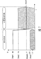
图10表示的是在一个复位时段中,来自图9所示复位电路的电压。FIG. 10 shows the voltages from the reset circuit shown in FIG. 9 during a reset period.
图11是根据本发明第三实施例的复位电路的电路方框图。FIG. 11 is a circuit block diagram of a reset circuit according to a third embodiment of the present invention.
图12表示的是在一个复位时段中,来自图11所示复位电路的电压。Figure 12 shows the voltages from the reset circuit shown in Figure 11 during a reset period.
图13是根据本发明第四实施例的复位电路的电路方框图。FIG. 13 is a circuit block diagram of a reset circuit according to a fourth embodiment of the present invention.
图14表示的是在一个复位时段中,来自图13所示复位电路的电压。FIG. 14 shows the voltages from the reset circuit shown in FIG. 13 during a reset period.
具体实施方式 Detailed ways
参考图6和图7,在一个复位时段中,根据本发明第一实施例的液晶显示器(LCD)提高公共电极与像素电极之间的电压差。在复位时段中,液晶分子被从张开状态快速转换成弯曲状态,这样,对下一个正常驱动间隔来说,液晶是处于弯曲状态的。为此目的,OCB模式中的液晶单元包括一个复位电路。6 and 7, in a reset period, the liquid crystal display (LCD) according to the first embodiment of the present invention increases the voltage difference between the common electrode and the pixel electrode. During the reset period, the liquid crystal molecules are rapidly switched from the open state to the bent state, so that for the next normal driving interval, the liquid crystal is in the bent state. For this purpose, the liquid crystal cell in OCB mode includes a reset circuit.
如图6所示,复位电路包括:一个数字视频卡60,用于将模拟信号转换成数字视频数据;一个电源64,用于施加驱动电压;一个数据驱动器66,用于将视频数据提供到LCD板(未示出)的数据线上;一个选通驱动器68,用于顺序驱动LCD板的选通线GL;一个控制器62,用于控制数据驱动器66和选通驱动器68;一个γ电压产生器70,用于将一个γ电压施加到数据驱动器66上;一个第一开关S1,用于选择一个提供给公共电极的公共电压Vcom;以及一个第二开关S2,用于选择一个在把像素电压提供给像素电极时使用的基准电压。As shown in Figure 6, the reset circuit includes: a
在LCD板中,液晶被注入两个玻璃基板之间。选通线GL与数据线DL以相互垂直方式形成于下玻璃基板之上。在接近各个选通线GL与数据线DL之间交点的区域都放置了一个薄膜晶体管(TFT),用于把数据线DL输入的图像数据有选择地施加于液晶单元。为此目的,TFT具有一个连接到选通线GL的栅极端(未示出)和一个连接到数据线DL的源极端(未示出)。TFT的漏极端(未示出)被连接至液晶单元的一个像素电极。In LCD panels, liquid crystals are injected between two glass substrates. The gate lines GL and the data lines DL are formed on the lower glass substrate in a manner perpendicular to each other. A thin film transistor (TFT) is placed near the intersection of each gate line GL and data line DL for selectively applying the image data input by the data line DL to the liquid crystal unit. For this purpose, the TFT has a gate terminal (not shown) connected to the gate line GL and a source terminal (not shown) connected to the data line DL. A drain terminal (not shown) of the TFT is connected to one pixel electrode of the liquid crystal cell.
数字视频卡60将模拟图像信号转换成适于LCD板的数字图像信号,并对包含在图像信号中的同步信号进行检测。控制器62从数字视频卡60接收一个电压范围在0~3.3V的驱动电压。控制器62将红、绿、蓝色数字视频数据提供给数据驱动器66。此外,控制器62还使用从数字视频卡60输入的水平/垂直同步信号H和V来产生一个点时钟Dclk和一个选通启动脉冲GSP,以便提供数据驱动器66和选通驱动器68的定时控制。具体地说,点时钟Dclk控制数据驱动器66,而选通启动脉冲GSP则控制选通驱动器68。The
电源64接收一个来自数字视频卡60,范围在0~3.3V的低电平公共电压,以便产生用于驱动液晶单元和选通驱动器68的驱动电压。电源64将0~3.3V的低电平公共电压VCC转换成15V的高电平公共电压VDD。根据控制器62所控制的第二开关S2的一个选择,电压VDD或0~3.3V的低电平电压VCC被作为基准电压,经由γ电压产生器70和数据驱动器66提供给像素电极。The
考虑到LCD板的电学和光学特性,γ电压产生器70产生一个与数据灰度级的值相一致的γ电压Vγ。来自控制器62的点时钟Dclk与红、绿、蓝色数字视频数据一起被输入数据驱动器66。数据驱动器66与点时钟Dclk同步地把红、绿、蓝色数字视频数据锁存,然后根据γ电压Vγ来对锁存数据进行校正。此外,数据驱动器66还把经过γ电压Vγ校正的各个红、绿、蓝色数字数据转换成应用于LCD板的数据线DL的相应的红、绿、蓝色模拟数据。The
电源64产生一个选通高电压VGH和一个选通低电压VGL,用于一个与选通扫描时钟GSC相一致的扫描信号。举例来说,电源64将0~3.3V的低电平公共电压VCC转换成一个20V的选通高电压VGH和一个-5V的选通低电压VGL,从而将它们施加到选通驱动器68上。The
选通驱动器68包括:一个移位寄存器,它响应于控制器62所输入的选通启动脉冲GSP,顺序产生一个扫描脉冲;以及一个电平移动器,用于将扫描脉冲的电压变换成适于驱动液晶单元的电压电平。选通驱动器68将一个选通高电压VGH和一个选通低电压VGL提供给液晶显示板40,以便应用于任意一条选通线GL。这个具有选通高电压VGH的扫描脉冲导通一个TFT开关,并将来自数据驱动器66的视频数据提供至液晶单元。The
控制器62使用一个控制信号来控制第一开关S1,根据第一开关S1的选择,把一个利用电阻器从高电平公共电压VDD中分压出的降低的电压或是选通高电压VGH与公共电极耦合。当第一开关S1选择使用电阻器来从高电平公共电压VDD中分压出一个降低的电压时,0~7V的公共电压Vcom将被提供给公共电极。否则,当第一开关S1选择选通高电压VGL时,20V的选通高电压VGH将被提供给公共电极。The
控制器62用一个控制信号来控制第二开关S2,根据其选择,低电平公共电压VCC或高电平公共电压VDD作为基准电压而被用于像素电极。当第二开关S2与低电平公共电压VCC耦合时,低电平公共电压VCC被作为基准电压,经由γ电压产生器70提供给数据驱动器66,以便为像素电极提供一个0~3.3V的真实数据信号。另一方面,当第二开关S2与高电平公共电压VDD耦合时,高电平公共电压VDD被作为基准电压,经由γ电压产生器70提供给数据驱动器66,以便为像素电极提供一个0~15V的真实数据信号。The
在OCB模式的液晶单元的液晶中,当像素电压与公共电压之间的差值增加时,从张开状态到弯曲状态的转换时间将会加快。显示转换时间与液晶单元电压差之间关系的实验结果在以下表格中被示出。In the liquid crystal of the OCB mode liquid crystal cell, when the difference between the pixel voltage and the common voltage increases, the transition time from the opened state to the bent state will be accelerated. Experimental results showing the relationship between switching time and liquid crystal cell voltage difference are shown in the following table.
表格1Table 1
结合图8来参考表1,可以看出,随着跨越液晶单元的电压差或电场增加,液晶从张开状态转换成弯曲状态所需要的时间将会减少。因此,在复位时段中,增加液晶单元的像素电极与公共电极之间的电压会导致液晶内部从张开状态到弯曲状态的快速转换。Referring to Table 1 in conjunction with Figure 8, it can be seen that as the voltage difference or electric field across the liquid crystal cell increases, the time required for the liquid crystal to transition from the stretched state to the curved state decreases. Therefore, during the reset period, increasing the voltage between the pixel electrode and the common electrode of the liquid crystal cell results in a rapid transition from the stretched state to the bent state inside the liquid crystal.
举例来说,响应于复位时段中来自控制器62的控制信号,第一开关S1与选通高电压VGH耦合,从而将选通高电压VGH提供给公共电极,而第二开关S2与作为基准电压的低电平公共电压VCC耦合,从而将低电平公共电压VCC经由γ电压产生器70和数据驱动器66提供给像素电极。因此,20V的选通高电压VGH被提供给公共电极,而变化宽度为0~3.3V的真实数据信号则被提供给像素电极。为了方便说明,如果假定一个1.7V的平均电压,那么将跨越该液晶产生一个大约18V的电压差。在这种情况下,如图8所示,液晶分子被从张开状态转换成弯曲状态,其转换时间大约在0.1秒以内。For example, in response to a control signal from the
在复位时段之后存在一个正常驱动间隔,其中大约7V的像素公共电压Vcom被提供给公共电极,而一个真实数据信号则被提供给像素电极。在正常驱动间隔中,液晶分子根据控制器62的控制信号而被从弯曲状态控制。如图7所示,在复位时段中,平均起来,像素电极与公共电极之间的电压差要大于所述正常驱动间隔中的真实数据信号。因此,在复位时段中,短时间就可将液晶从张开状态转换成弯曲状态。After the reset period, there is a normal driving interval in which the pixel common voltage Vcom of about 7V is supplied to the common electrode and a real data signal is supplied to the pixel electrode. In a normal driving interval, liquid crystal molecules are controlled from a bent state according to a control signal of the
在第二实施例中,如图9所示,在复位时段中,第一开关S1将选通高电压VGH与公共电极耦合以作为公共电压Vcom,而第二开关S2则耦合高电平公共电压VDD以作为用于像素电极的基准电压。响应于来自控制器62的控制信号,第一开关S1被耦合到选通高电压VGH,从而将选通高电压VGH施加到公共电极上。第二开关S2则耦合到作为基准电压的高电平公共电压VDD,从而将高电平公共电压VDD经由γ电压产生器70和数据驱动器66提供给像素电极。因此,如图10所示,20V的电压被提供给公共电极,而变化宽度为0~15V的真实数据信号则被提供给像素电极。为了方便说明,如果假定一个7V的平均电压,那么跨越液晶单元将会产生一个大约13V的电压差。在这种情况下,如图8所示,液晶分子在少于0.5秒的时间里被从张开状态转换成弯曲状态。In the second embodiment, as shown in FIG. 9, in the reset period, the first switch S1 couples the gate high voltage VGH to the common electrode as the common voltage Vcom, and the second switch S2 couples the high-level common voltage VDD is used as a reference voltage for the pixel electrode. In response to a control signal from the
在复位时段之后存在一个正常驱动间隔,其中大约为7V的像素公共电压Vcom被提供给公共电极,而一个真实数据信号则被提供给像素电极。在正常驱动间隔中,液晶分子根据控制器62的控制信号而被从弯曲状态控制。如图10所示,在复位时段中,像素电极与公共电极之间的电压差要大于所述正常驱动间隔中的真实数据信号的平均电压。因此,在复位时段中,短时间内就可将液晶从张开状态转换成弯曲状态。After the reset period, there is a normal driving interval in which the pixel common voltage Vcom of about 7V is supplied to the common electrode and a real data signal is supplied to the pixel electrode. In a normal driving interval, liquid crystal molecules are controlled from a bent state according to a control signal of the
在第三实施例中,如图11所示,第一开关S1被耦合到一个用电阻器从高电平公共电压VDD分压出的降低电压,而第二开关S2则被耦合到一个低电平公共电压VCC。响应于来自控制器62的控制信号,第一开关S1耦合到使用电阻器从高电平公共电压VDD分压出的降低电压,从而将像素公共电压Vcom提供给公共电极。第二开关S2耦合低电平公共电压VCC作为基准电压,以便用在像素电极上。因此,如图12所示,一个7V的电压被提供给公共电极,并且变化宽度为0~3.3V的真实数据信号被提供给像素电极。为了方便说明,如果假定存在一个1.7V的平均电压,那么跨越液晶单元将会产生一个大约5~6V的电压差。在这种情况下,如图8所示,液晶分子将在大约12~44秒内从张开状态转换到弯曲状态。In the third embodiment, as shown in FIG. 11, the first switch S1 is coupled to a reduced voltage divided by a resistor from the high-level common voltage VDD, and the second switch S2 is coupled to a low-level voltage. level common voltage VCC. In response to a control signal from the
在复位时段后,一个大约为7V的公共电压Vcom被提供到公共电极,而一个真实数据信号则被提供给像素电极,从而根据控制器62的控制信号,在正常驱动间隔中从弯曲状态提供液晶分子的正常驱动。如图12所示,在复位时段中,像素电极与公共电极之间的电压差要大于所述正常驱动间隔中的真实数据信号的平均电压。因此,在复位时段中,液晶可以在短时间内从张开状态转换成弯曲状态。After the reset period, a common voltage Vcom of about 7V is supplied to the common electrode, and a real data signal is supplied to the pixel electrode, thereby supplying the liquid crystal from the bent state in the normal driving interval according to the control signal of the
参考图13,根据本发明第四实施例的LCD在复位时段中把正常驱动间隔中提供的最大驱动电压施加到像素电极,由此使得液晶分子能够快速从张开状态转换至弯曲状态。为此目的,如图13所示,OCB模式中的液晶单元包括一个复位电路。Referring to FIG. 13 , the LCD according to the fourth embodiment of the present invention applies the maximum driving voltage provided in the normal driving interval to the pixel electrodes in the reset period, thereby enabling the liquid crystal molecules to quickly switch from the opened state to the bent state. For this purpose, as shown in FIG. 13, the liquid crystal cell in the OCB mode includes a reset circuit.
复位电路包括:一个数字视频卡60,用于将模拟视频信号转换成数字视频数据;一个电源64,用于施加驱动电压;一个数据驱动器66,用于将视频数据提供到液晶显示板(未示出)的数据线上;一个选通驱动器68,用于顺序驱动液晶显示板的选通线GL;一个控制器62,用于控制数据驱动器66和选通驱动器68;一个γ电压产生器70,用于将一个γ电压施加到数据驱动器66上;一个电阻器R,用于将一个降低的电压作为公共电压Vcom提供给公共电极,该电压是利用电阻器R分割高电平公共电压VDD得到的。The reset circuit includes: a
在液晶显示板中,液晶被注入两个玻璃基板之间,选通线GL与数据线DL以相互垂直这样一种方式形成于下玻璃基板之上。数字视频卡60将模拟输入图像信号转换成适于液晶显示板的数字图像信号,并对包含在模拟输入图像信号中的同步信号进行检测。控制器62从数字视频卡60接收一个电压范围是0~3.3V的驱动电压。控制器62将红、绿、蓝色数字视频数据提供给数据驱动器66。此外,控制器62使用数字视频卡60输入的水平/垂直同步信号H和V来产生一个点时钟Dclk和一个选通启动脉冲GSP,以便提供对数据驱动器66和选通驱动器68的定时控制。具体地说,点时钟Dclk控制数据驱动器66,而选通启动脉冲GSP则控制选通驱动器68。In the liquid crystal display panel, liquid crystal is injected between two glass substrates, and gate lines GL and data lines DL are formed on the lower glass substrate in such a manner that they are perpendicular to each other. The
电源64接收一个来自数字视频卡60,范围是0~3.3V的低电平公共电压,以便产生一个用于驱动液晶单元的高电平公共电压VDD和用于驱动选通驱动器68的电压。高电平公共电压VDD被一个分压电阻器R分成一个用于7V公共电压Vcom的降低电压,公共电压Vcom经由液晶显示板焊盘部分上的一个Ag点而被提供给液晶显示板的上基板上提供的公共电极。根据选通扫描时钟GSC,电源64产生扫描信号的一个选通高电压VGH和一个选通低电压VGL。举例来说,电源64将所供应的0~3.3V的低电平公共电压VCC转换成一个20V的选通高电压VGH和一个-5V的选通低电压VGL。选通高电压VGH与-5V的选通低电压VGL都被提供给选通驱动器68。The
选通驱动器68包括:一个移位寄存器,用于响应从控制器62输入的选通启动脉冲GSP来顺序产生一个扫描脉冲;以及一个电平移动器,用于将扫描脉冲的电压变换成适于驱动液晶单元的电压电平。选通驱动器68沿着选通线GL,将一个选通高电压VGH和一个选通低电压VGL提供给液晶显示板40。这个具有选通高电压VGH的扫描脉冲导通一个TFT开关,并将来自数据驱动器66的视频数据提供到液晶单元中。The
来自控制器62的点时钟Dclk与红、绿、蓝色数字视频数据一起被输入数据驱动器66。数据驱动器66与点时钟Dclk同步地锁存红、绿、蓝色数字视频数据,然后根据γ电压Vγ来对锁存数据进行校正。此外,数据驱动器66还将一个经过γ电压Vγ校正的数据转换成模拟数据,从而将其施加到数据线DL,用于各条线。The dot clock Dclk from the
如图14所示,在复位时段中,响应于来自控制器62的控制信号,馈送到数据驱动器66的15V的最大驱动电压被供应到像素电极。此外,用于7V公共电压Vcom的降低电压被提供给液晶单元的公共电极。控制器62产生一个控制信号,用于提供一个延迟,这样一来,在复位时段中,真实数据信号并未提供给像素电极。响应于这个控制信号,真实数据信号只在正常驱动间隔中被提供。换句话说,在复位时段之后,一个7V的电压被提供给公共电极,一个真实数据信号在正常驱动间隔中用于像素电极。As shown in FIG. 14 , in the reset period, a maximum driving voltage of 15V fed to the
如图14所示,真实数据信号的最高电压在复位时段被提供给像素电极,由此使复位时段中跨越液晶单元的电压差能被设置成在真实驱动中可以得到的跨越液晶单元的最大电压差。在复位时段中提供给像素电极的电压是一个最大恒定驱动电压,而在真实驱动中提供给像素电极的真实数据信号则是变化的,其平均值要小于复位时段中提供的最大驱动电压。因此,在复位时段中像素电极与公共电极之间的电压差要大于所述正常驱动间隔中的真实数据信号的平均电压,以使液晶能在复位时段中被快速从张开状态转换至弯曲状态。As shown in Figure 14, the highest voltage of the real data signal is supplied to the pixel electrode during the reset period, thereby enabling the voltage difference across the liquid crystal cell during the reset period to be set to the maximum voltage across the liquid crystal cell that can be obtained in real driving Difference. The voltage provided to the pixel electrode in the reset period is a maximum constant driving voltage, while the real data signal provided to the pixel electrode in the actual driving varies, and its average value is smaller than the maximum driving voltage provided in the reset period. Therefore, the voltage difference between the pixel electrode and the common electrode in the reset period is greater than the average voltage of the real data signal in the normal driving interval, so that the liquid crystal can be quickly switched from the opened state to the curved state in the reset period. .
如上所述,根据本发明,在复位时段中提供给液晶单元的最大恒定驱动电压要大于在液晶显示器的正常驱动中提供的真实数据信号的平均电压。因此,液晶可以快速从张开状态转换至弯曲状态。As described above, according to the present invention, the maximum constant driving voltage supplied to the liquid crystal cell in the reset period is larger than the average voltage of the real data signal supplied in the normal driving of the liquid crystal display. Therefore, the liquid crystal can quickly switch from the stretched state to the curved state.
对本领域技术人员来说,可以在用于制造本发明的液晶显示器的设备和方法中进行各种修改与变化,而不脱离本发明的实质或范围,这一点是显而易见的。因此,本发明包含归入附加权利要求及其等价物的围中的所有修改和变化。It will be apparent to those skilled in the art that various modifications and changes can be made in the apparatus and method for manufacturing the liquid crystal display of the present invention without departing from the spirit or scope of the invention. Accordingly, the present invention includes all modifications and changes that come within the scope of the appended claims and their equivalents.
Claims (3)
Applications Claiming Priority (2)
| Application Number | Priority Date | Filing Date | Title |
|---|---|---|---|
| KR1020010085966A KR100843685B1 (en) | 2001-12-27 | 2001-12-27 | Method and apparatus for driving a liquid crystal display |
| KR85966/2001 | 2001-12-27 |
Publications (2)
| Publication Number | Publication Date |
|---|---|
| CN1428761A CN1428761A (en) | 2003-07-09 |
| CN100433112C true CN100433112C (en) | 2008-11-12 |
Family
ID=19717679
Family Applications (1)
| Application Number | Title | Priority Date | Filing Date |
|---|---|---|---|
| CNB021586691A Expired - Fee Related CN100433112C (en) | 2001-12-27 | 2002-12-19 | Apparatus and method for driving liquid crystal display |
Country Status (4)
| Country | Link |
|---|---|
| US (1) | US7202864B2 (en) |
| JP (2) | JP3999119B2 (en) |
| KR (1) | KR100843685B1 (en) |
| CN (1) | CN100433112C (en) |
Families Citing this family (21)
| Publication number | Priority date | Publication date | Assignee | Title |
|---|---|---|---|---|
| EP1582911A4 (en) * | 2003-01-08 | 2007-08-08 | Toshiba Matsushita Display Tec | Liquid crystal display |
| KR100951358B1 (en) * | 2003-09-05 | 2010-04-08 | 삼성전자주식회사 | Liquid crystal display and its driving device |
| US7388565B2 (en) * | 2003-12-02 | 2008-06-17 | Stmicroelectronics Pvt. Ltd. | LCD driver with adjustable contrast |
| JP4528774B2 (en) * | 2004-02-20 | 2010-08-18 | 東芝モバイルディスプレイ株式会社 | Liquid crystal display |
| JP2006047848A (en) * | 2004-08-06 | 2006-02-16 | Toshiba Matsushita Display Technology Co Ltd | Gate line driving circuit |
| JP2006053428A (en) * | 2004-08-13 | 2006-02-23 | Toshiba Matsushita Display Technology Co Ltd | Gate line driving circuit |
| KR20060020075A (en) * | 2004-08-31 | 2006-03-06 | 삼성전자주식회사 | Drive unit and display device having same |
| JP4528598B2 (en) * | 2004-10-22 | 2010-08-18 | 東芝モバイルディスプレイ株式会社 | Liquid crystal display |
| KR100731726B1 (en) * | 2004-12-10 | 2007-06-22 | 삼성에스디아이 주식회사 | Liquid Crystal Display Having OCC Mode and Driving Method Thereof |
| JP4442455B2 (en) * | 2005-02-17 | 2010-03-31 | セイコーエプソン株式会社 | Reference voltage selection circuit, reference voltage generation circuit, display driver, electro-optical device, and electronic apparatus |
| TWI327303B (en) * | 2006-03-17 | 2010-07-11 | Chimei Innolux Corp | Optically compensated bend liquid crystal display device |
| KR101189090B1 (en) * | 2006-07-18 | 2012-11-09 | 삼성디스플레이 주식회사 | LCD and its driving method |
| KR101272333B1 (en) | 2006-09-27 | 2013-06-10 | 삼성디스플레이 주식회사 | LIQUID CRYSTAL DISPLAY and DRIVING MATHOD THEREOF |
| WO2009011150A1 (en) * | 2007-07-18 | 2009-01-22 | Sharp Kabushiki Kaisha | Display device and its driving method |
| KR101410955B1 (en) | 2007-07-20 | 2014-07-03 | 삼성디스플레이 주식회사 | Display apparatus and method of driving the display apparatus |
| KR101011508B1 (en) * | 2008-12-29 | 2011-01-31 | 주식회사 포스코플랜텍 | Hydraulic cylinder for water gate opening and shutting |
| KR102081132B1 (en) * | 2013-12-30 | 2020-02-25 | 엘지디스플레이 주식회사 | Organic Light Emitting Display |
| JP2017009853A (en) * | 2015-06-24 | 2017-01-12 | 株式会社ジャパンディスプレイ | Display device |
| CN108320715A (en) * | 2018-01-03 | 2018-07-24 | 惠科股份有限公司 | Liquid crystal display device and driving method thereof |
| CN108389558B (en) * | 2018-03-23 | 2020-08-25 | 京东方科技集团股份有限公司 | Voltage applying circuit, display device and method for applying common voltage signal |
| JP7333701B2 (en) * | 2019-03-08 | 2023-08-25 | 日東電工株式会社 | Polymer-dispersed liquid crystal device and method for driving polymer-dispersed liquid crystal panel |
Citations (4)
| Publication number | Priority date | Publication date | Assignee | Title |
|---|---|---|---|---|
| CN1160260A (en) * | 1995-12-22 | 1997-09-24 | 国际商业机器公司 | Driving method of liquid crystal display device |
| US6005543A (en) * | 1997-02-21 | 1999-12-21 | Kabushiki Kaisha Toshiba | Liquid crystal display device and method of driving the same |
| US6320571B1 (en) * | 1997-09-12 | 2001-11-20 | Ricoh Company, Ltd. | Bistable liquid crystal display device |
| CN1327546A (en) * | 1999-10-19 | 2001-12-19 | 松下电器产业株式会社 | Drive technique for starting liquid crystal device |
Family Cites Families (15)
| Publication number | Priority date | Publication date | Assignee | Title |
|---|---|---|---|---|
| US5933199A (en) * | 1995-09-15 | 1999-08-03 | Lg Electronics Inc. | Gamma correction circuit using analog multiplier |
| JP3240367B2 (en) * | 1995-11-13 | 2001-12-17 | シャープ株式会社 | Active matrix type liquid crystal image display |
| JP3526996B2 (en) | 1995-12-28 | 2004-05-17 | 富士通ディスプレイテクノロジーズ株式会社 | Driving method of liquid crystal display device |
| JPH10206822A (en) | 1997-01-20 | 1998-08-07 | Internatl Business Mach Corp <Ibm> | Voltage application driving system |
| KR100251543B1 (en) * | 1997-07-28 | 2000-04-15 | 구본준 | Gradation correction voltage supply device |
| JP3183654B2 (en) | 1998-09-03 | 2001-07-09 | 松下電器産業株式会社 | Liquid crystal display device and driving method thereof |
| JP2001296519A (en) | 1998-09-03 | 2001-10-26 | Matsushita Electric Ind Co Ltd | Liquid crystal display device, method of manufacturing the same, and method of driving liquid crystal display device |
| EP1235101A3 (en) * | 1998-09-03 | 2008-08-20 | Toshiba Matsushita Display Technology Co., Ltd. | Liquid crystal display device, method for manufacturing the same, and method for driving a liquid crystal display device |
| JP4528455B2 (en) | 1999-03-15 | 2010-08-18 | 東芝モバイルディスプレイ株式会社 | Liquid crystal display |
| JP2001083552A (en) | 1999-03-15 | 2001-03-30 | Matsushita Electric Ind Co Ltd | Liquid crystal display device, method of manufacturing the same, and method of driving liquid crystal display device |
| JP4236791B2 (en) | 1999-03-26 | 2009-03-11 | 株式会社半導体エネルギー研究所 | Liquid crystal display device, display, projector, goggle type display, portable information terminal, and computer |
| JP3886698B2 (en) | 1999-03-31 | 2007-02-28 | 株式会社半導体エネルギー研究所 | Liquid crystal display device, driving method of liquid crystal display device, display, projector, goggle type display, portable information terminal, and computer |
| JP2000321556A (en) | 1999-05-14 | 2000-11-24 | Sanyo Electric Co Ltd | Method for transition of alignment state of liquid crystal and method of driving liquid crystal display device |
| EP1113412B1 (en) | 1999-12-27 | 2014-05-21 | Japan Display Inc. | Liquid crystal display apparatus and method for driving the same |
| JP3565324B2 (en) | 2000-04-10 | 2004-09-15 | シャープ株式会社 | Driving method of liquid crystal display device |
-
2001
- 2001-12-27 KR KR1020010085966A patent/KR100843685B1/en not_active Expired - Fee Related
-
2002
- 2002-10-11 US US10/268,836 patent/US7202864B2/en not_active Expired - Fee Related
- 2002-12-19 CN CNB021586691A patent/CN100433112C/en not_active Expired - Fee Related
- 2002-12-20 JP JP2002371082A patent/JP3999119B2/en not_active Expired - Fee Related
-
2007
- 2007-05-25 JP JP2007138820A patent/JP4359631B2/en not_active Expired - Fee Related
Patent Citations (4)
| Publication number | Priority date | Publication date | Assignee | Title |
|---|---|---|---|---|
| CN1160260A (en) * | 1995-12-22 | 1997-09-24 | 国际商业机器公司 | Driving method of liquid crystal display device |
| US6005543A (en) * | 1997-02-21 | 1999-12-21 | Kabushiki Kaisha Toshiba | Liquid crystal display device and method of driving the same |
| US6320571B1 (en) * | 1997-09-12 | 2001-11-20 | Ricoh Company, Ltd. | Bistable liquid crystal display device |
| CN1327546A (en) * | 1999-10-19 | 2001-12-19 | 松下电器产业株式会社 | Drive technique for starting liquid crystal device |
Also Published As
| Publication number | Publication date |
|---|---|
| KR100843685B1 (en) | 2008-07-04 |
| JP3999119B2 (en) | 2007-10-31 |
| JP2003202546A (en) | 2003-07-18 |
| US7202864B2 (en) | 2007-04-10 |
| US20030122753A1 (en) | 2003-07-03 |
| CN1428761A (en) | 2003-07-09 |
| KR20030055851A (en) | 2003-07-04 |
| JP2007226271A (en) | 2007-09-06 |
| JP4359631B2 (en) | 2009-11-04 |
Similar Documents
| Publication | Publication Date | Title |
|---|---|---|
| CN100433112C (en) | Apparatus and method for driving liquid crystal display | |
| US20070132697A1 (en) | Liquid crystal display and driving method thereof | |
| US7019728B2 (en) | LCD for speeding initial bend state, driver and method thereof | |
| JP4685954B2 (en) | Liquid crystal display device having OCB mode and driving method thereof | |
| US20070296682A1 (en) | Liquid crystal display device and driving method thereof | |
| KR100883270B1 (en) | LCD and its driving method | |
| KR102143221B1 (en) | Display Device | |
| US20080084412A1 (en) | Liquid crystal display device and method for driving the same | |
| US20110102695A1 (en) | Liquid crystal display device driving method and liquid crystal display device | |
| CN100480821C (en) | Liquid crystal display device and method of driving the same | |
| US20060125813A1 (en) | Active matrix liquid crystal display with black-inserting circuit | |
| US7675496B2 (en) | Liquid crystal display and driving method thereof | |
| US20040239609A1 (en) | Liquid crystal display, method and apparatus for driving the same | |
| KR100783704B1 (en) | Liquid Crystal Display and driving apparatus and method thereof | |
| KR20040073703A (en) | Driving Methode for Liquid Crystal Display device and Driving Circuit at the same | |
| KR100656916B1 (en) | Liquid crystal display, drive device and method thereof for increasing initial bend orientation | |
| KR100870516B1 (en) | LCD and its driving method | |
| KR100864974B1 (en) | LCD Display | |
| KR100511877B1 (en) | Method for driving of lcd | |
| US20040222957A1 (en) | [a line inversion drive device for thin film transistor liquid crystal display] | |
| KR100476390B1 (en) | Stn lcd driving circuit for low voltage element | |
| US20110310321A1 (en) | Method of driving liquid crystal display device, and liquid crystal display device | |
| US20070146264A1 (en) | Liquid crystal display and driving method thereof | |
| US20060139277A1 (en) | Active matrix liquid crystal display with black image | |
| KR20030030077A (en) | METHOD AND APPARATuS FOR DRIVING LIQuID CRYSTAL DISPLAY |
Legal Events
| Date | Code | Title | Description |
|---|---|---|---|
| C06 | Publication | ||
| PB01 | Publication | ||
| C10 | Entry into substantive examination | ||
| SE01 | Entry into force of request for substantive examination | ||
| C14 | Grant of patent or utility model | ||
| GR01 | Patent grant | ||
| CF01 | Termination of patent right due to non-payment of annual fee | ||
| CF01 | Termination of patent right due to non-payment of annual fee |
Granted publication date: 20081112 Termination date: 20171219 |