CN100433343C - Solid-state imaging device and manufacturing method thereof - Google Patents
Solid-state imaging device and manufacturing method thereof Download PDFInfo
- Publication number
- CN100433343C CN100433343C CNB2004100752118A CN200410075211A CN100433343C CN 100433343 C CN100433343 C CN 100433343C CN B2004100752118 A CNB2004100752118 A CN B2004100752118A CN 200410075211 A CN200410075211 A CN 200410075211A CN 100433343 C CN100433343 C CN 100433343C
- Authority
- CN
- China
- Prior art keywords
- rib
- housing
- inner end
- lead
- metal lead
- Prior art date
- Legal status (The legal status is an assumption and is not a legal conclusion. Google has not performed a legal analysis and makes no representation as to the accuracy of the status listed.)
- Expired - Fee Related
Links
Images


Classifications
-
- H—ELECTRICITY
- H10—SEMICONDUCTOR DEVICES; ELECTRIC SOLID-STATE DEVICES NOT OTHERWISE PROVIDED FOR
- H10F—INORGANIC SEMICONDUCTOR DEVICES SENSITIVE TO INFRARED RADIATION, LIGHT, ELECTROMAGNETIC RADIATION OF SHORTER WAVELENGTH OR CORPUSCULAR RADIATION
- H10F39/00—Integrated devices, or assemblies of multiple devices, comprising at least one element covered by group H10F30/00, e.g. radiation detectors comprising photodiode arrays
- H10F39/10—Integrated devices
- H10F39/12—Image sensors
-
- H—ELECTRICITY
- H10—SEMICONDUCTOR DEVICES; ELECTRIC SOLID-STATE DEVICES NOT OTHERWISE PROVIDED FOR
- H10F—INORGANIC SEMICONDUCTOR DEVICES SENSITIVE TO INFRARED RADIATION, LIGHT, ELECTROMAGNETIC RADIATION OF SHORTER WAVELENGTH OR CORPUSCULAR RADIATION
- H10F39/00—Integrated devices, or assemblies of multiple devices, comprising at least one element covered by group H10F30/00, e.g. radiation detectors comprising photodiode arrays
- H10F39/80—Constructional details of image sensors
- H10F39/804—Containers or encapsulations
-
- H—ELECTRICITY
- H10—SEMICONDUCTOR DEVICES; ELECTRIC SOLID-STATE DEVICES NOT OTHERWISE PROVIDED FOR
- H10F—INORGANIC SEMICONDUCTOR DEVICES SENSITIVE TO INFRARED RADIATION, LIGHT, ELECTROMAGNETIC RADIATION OF SHORTER WAVELENGTH OR CORPUSCULAR RADIATION
- H10F77/00—Constructional details of devices covered by this subclass
- H10F77/50—Encapsulations or containers
-
- H—ELECTRICITY
- H10—SEMICONDUCTOR DEVICES; ELECTRIC SOLID-STATE DEVICES NOT OTHERWISE PROVIDED FOR
- H10W—GENERIC PACKAGES, INTERCONNECTIONS, CONNECTORS OR OTHER CONSTRUCTIONAL DETAILS OF DEVICES COVERED BY CLASS H10
- H10W99/00—Subject matter not provided for in other groups of this subclass
-
- H—ELECTRICITY
- H10—SEMICONDUCTOR DEVICES; ELECTRIC SOLID-STATE DEVICES NOT OTHERWISE PROVIDED FOR
- H10W—GENERIC PACKAGES, INTERCONNECTIONS, CONNECTORS OR OTHER CONSTRUCTIONAL DETAILS OF DEVICES COVERED BY CLASS H10
- H10W72/00—Interconnections or connectors in packages
- H10W72/01—Manufacture or treatment
- H10W72/0198—Manufacture or treatment batch processes
-
- H—ELECTRICITY
- H10—SEMICONDUCTOR DEVICES; ELECTRIC SOLID-STATE DEVICES NOT OTHERWISE PROVIDED FOR
- H10W—GENERIC PACKAGES, INTERCONNECTIONS, CONNECTORS OR OTHER CONSTRUCTIONAL DETAILS OF DEVICES COVERED BY CLASS H10
- H10W72/00—Interconnections or connectors in packages
- H10W72/50—Bond wires
- H10W72/531—Shapes of wire connectors
- H10W72/536—Shapes of wire connectors the connected ends being ball-shaped
-
- H—ELECTRICITY
- H10—SEMICONDUCTOR DEVICES; ELECTRIC SOLID-STATE DEVICES NOT OTHERWISE PROVIDED FOR
- H10W—GENERIC PACKAGES, INTERCONNECTIONS, CONNECTORS OR OTHER CONSTRUCTIONAL DETAILS OF DEVICES COVERED BY CLASS H10
- H10W72/00—Interconnections or connectors in packages
- H10W72/50—Bond wires
- H10W72/531—Shapes of wire connectors
- H10W72/5363—Shapes of wire connectors the connected ends being wedge-shaped
-
- H—ELECTRICITY
- H10—SEMICONDUCTOR DEVICES; ELECTRIC SOLID-STATE DEVICES NOT OTHERWISE PROVIDED FOR
- H10W—GENERIC PACKAGES, INTERCONNECTIONS, CONNECTORS OR OTHER CONSTRUCTIONAL DETAILS OF DEVICES COVERED BY CLASS H10
- H10W72/00—Interconnections or connectors in packages
- H10W72/50—Bond wires
- H10W72/541—Dispositions of bond wires
- H10W72/5449—Dispositions of bond wires not being orthogonal to a side surface of the chip, e.g. fan-out arrangements
-
- H—ELECTRICITY
- H10—SEMICONDUCTOR DEVICES; ELECTRIC SOLID-STATE DEVICES NOT OTHERWISE PROVIDED FOR
- H10W—GENERIC PACKAGES, INTERCONNECTIONS, CONNECTORS OR OTHER CONSTRUCTIONAL DETAILS OF DEVICES COVERED BY CLASS H10
- H10W72/00—Interconnections or connectors in packages
- H10W72/851—Dispositions of multiple connectors or interconnections
- H10W72/874—On different surfaces
- H10W72/884—Die-attach connectors and bond wires
-
- H—ELECTRICITY
- H10—SEMICONDUCTOR DEVICES; ELECTRIC SOLID-STATE DEVICES NOT OTHERWISE PROVIDED FOR
- H10W—GENERIC PACKAGES, INTERCONNECTIONS, CONNECTORS OR OTHER CONSTRUCTIONAL DETAILS OF DEVICES COVERED BY CLASS H10
- H10W74/00—Encapsulations, e.g. protective coatings
-
- H—ELECTRICITY
- H10—SEMICONDUCTOR DEVICES; ELECTRIC SOLID-STATE DEVICES NOT OTHERWISE PROVIDED FOR
- H10W—GENERIC PACKAGES, INTERCONNECTIONS, CONNECTORS OR OTHER CONSTRUCTIONAL DETAILS OF DEVICES COVERED BY CLASS H10
- H10W90/00—Package configurations
- H10W90/701—Package configurations characterised by the relative positions of pads or connectors relative to package parts
- H10W90/751—Package configurations characterised by the relative positions of pads or connectors relative to package parts of bond wires
- H10W90/756—Package configurations characterised by the relative positions of pads or connectors relative to package parts of bond wires between a chip and a stacked lead frame, conducting package substrate or heat sink
Landscapes
- Solid State Image Pick-Up Elements (AREA)
- Transforming Light Signals Into Electric Signals (AREA)
Abstract
一种固态成像装置,包括:壳体,其中基座和形成矩形框架的若干个肋通过树脂形成为一个部件;被埋置在壳体中的多个金属引线件,每个引线件具有面对壳体的内部空间的内端部和暴露在壳体的外部的外端部;安装在壳体的内部空间中的基座上的一个成像元件;将成像元件的电极连接到金属引线件的内端部的若干个连接件;和固定到肋的上表面的透明板。肋的上表面设有沿着外周边向下的下阶梯部分,并且透明板通过至少填充在下阶梯部分中的粘合剂固定到肋的上表面。肋和透明板之间的结合相对于由热变形等产生的应力具有缓冲效果,由此提高了耐久性。
A solid-state imaging device comprising: a case in which a base and several ribs forming a rectangular frame are formed as one part by resin; a plurality of metal lead parts embedded in the case, each lead part having a facing An inner end portion of the inner space of the housing and an outer end portion exposed to the outside of the housing; an imaging element installed on a base in the inner space of the housing; an inner end connecting an electrode of the imaging element to a metal lead member several connectors at the ends; and a transparent plate secured to the upper surface of the rib. The upper surface of the rib is provided with a lower stepped portion downward along the outer periphery, and the transparent plate is fixed to the upper surface of the rib by an adhesive filled at least in the lower stepped portion. The bonding between the rib and the transparent plate has a cushioning effect against stress generated by thermal deformation or the like, thereby improving durability.
Description
技术领域 technical field
本发明涉及固态成像装置及其制造方法,在所述固态成像装置中,成像元件(如CCD或类似元件)被安装在壳体中。The present invention relates to a solid-state imaging device in which an imaging element such as a CCD or the like is mounted in a housing and a method of manufacturing the same.
背景技术 Background technique
广泛用于摄像机和照像机等的固态成像装置以封装形式提供,其中成像元件如CCD等安装在由绝缘材料制成的基座上,光电检测区由透明板覆盖。为使这种装置更紧凑,将成像元件安装在基座上作为裸芯片。图10示出了在JP 2001-77277中公开的固态成像装置,这是这种固态成像装置的常规例子。Solid-state imaging devices widely used in video cameras, still cameras, etc. are provided in a package in which an imaging element such as a CCD etc. is mounted on a base made of an insulating material and a photodetection area is covered by a transparent plate. To make this device more compact, the imaging element is mounted on a base as a bare chip. FIG. 10 shows a solid-state imaging device disclosed in JP 2001-77277, which is a conventional example of such a solid-state imaging device.
在图10中,标记41表示由基座41a和框架形肋41b构成的壳体,其中框架形肋41b是通过树脂模制形成为一个部件。内部空间42形成在壳体41的上侧。位于基座41a的中心的冲模垫43和位于肋41b下面的引线44被埋置在壳体41中。位于内部空间42的中心的成像元件芯片45固定到冲模垫43的上侧。引线44包括内端部44a和外端部44b,其中内端部44a暴露于肋41b的内部侧上的基座41a上侧的内部空间42,可从肋41b下面的基座41a的底侧接触外端部44b。内端部44a和成像元件45的键合焊盘通过由金属制成的键合线46连接。透明密封玻璃板47固定到肋41b的上表面,由此形成用于保护成像元件芯片45的封装。In FIG. 10,
这种固态成像装置安装在电路板上,并使密封玻璃板47面朝上,如图10所示,使用外端部44b将其连接到电路板上的电极上。尽管图中未示出,结合成像光学系统的透镜镜筒安装在密封玻璃板47的顶部,其中成像光学系统相对于形成在成像元件芯片45中的光电检测区的相对位置可以以预定精度调整。在成像操作期间,已经经过了结合在透镜镜筒中的成像光学系统的物体光在光电检测区上聚焦并进行光电转换。This solid-state imaging device is mounted on the circuit board with the
具有这种构成的固态成像装置通过暴露在壳体底表面的外端部44b连接到电路板的电极上,因此封装的高度和占据的表面面积比使用从壳体周围向下弯曲的外部引线进行连接的情况小,由此使其适合于高密度封装。The solid-state imaging device having such a constitution is connected to the electrodes of the circuit board through the
在JP2001-77277A中公开的技术中,如图11所示的上模具48和下模具49用于进行如图10所示的壳体41的树脂模制。下模具49的上侧是平坦的。上模具48的下侧设有对应肋41b的凹部48a。在凹部48a的两侧提供形成内部空间42的内部突起部48b和形成肋41b的外表面的外部突起部48c。引线44和冲模垫43以与引线框架50成一体的形式提供,并设置在上模具48和下模具49之间。In the technique disclosed in JP2001-77277A, an
通过将引线框架50置于上模具48和下模具49之间,在下模具49和上模具48的内部突起部48b之间形成用于模制基座41a的腔51。在这种情况下,在其中填充树脂,将模具打开并取出模制产品,其中基座41a和肋41b形成具有它们的完成形式的壳体41。模制之后,在位于肋41b外侧的部位切割引线框架50。By placing the
在上述常规固态成像装置中,只在它们之间使用少量粘合剂就可以将密封玻璃板47连接到肋41b的上表面上。由于肋41b的上表面的面积很小,因此连接强度弱。此外,由于粘合剂层很薄,当在密封玻璃板47和肋41b之间由热变形产生应力时,由粘合剂层所做的变形缓冲很小,并且这两个部件之间的结合耐久性很低。In the conventional solid-state imaging device described above, the
发明内容 Contents of the invention
本发明的目的是提供一种固态成像装置,它具有在肋和位于肋上表面的透明板之间的结合部,并相对于由于热变形等在部件之间产生的应力而具有高耐久性。An object of the present invention is to provide a solid-state imaging device having a joint between a rib and a transparent plate on the upper surface of the rib and having high durability against stress generated between components due to thermal deformation or the like.
此外,本发明的目的是提供一种制造固态成像装置的方法,该方法通过将这样的结构应用于固态成像装置而适于批量生产,而不会使制造工艺复杂化。Furthermore, an object of the present invention is to provide a method of manufacturing a solid-state imaging device which is suitable for mass production by applying such a structure to the solid-state imaging device without complicating the manufacturing process.
根据本发明的固态成像装置,包括:壳体,其中基座和形成矩形框架的若干个肋通过树脂形成为一个部件;被埋置在壳体中的多个金属引线件,每个引线件具有面对壳体的内部空间的内端部、暴露在壳体的外部的外端部、和暴露在所述壳体的外侧面的横向电极部;成像元件,安装在壳体的内部空间中的基座上;连接件,将成像元件的电极连接到金属引线件的内端部;和透明板,固定在所述肋的上表面,其中,所述肋的上表面设有沿着外周边向下的下阶梯部分;该透明板通过至少填充在下阶梯部分中的粘合剂固定到所述肋的上表面;所述各金属引线件的所述横向电极部的下表面,被所述基座的树脂覆盖。A solid-state imaging device according to the present invention includes: a case in which a base and several ribs forming a rectangular frame are formed as one part by resin; a plurality of metal lead parts embedded in the case, each lead part having an inner end facing the inner space of the housing, an outer end exposed to the outside of the housing, and a lateral electrode portion exposed on the outer side of the housing; an imaging element installed in the inner space of the housing on the base; connecting parts, connecting the electrodes of the imaging element to the inner ends of the metal lead parts; and transparent plates, fixed on the upper surface of the rib, wherein the upper surface of the rib is provided with lower lower stepped portion; the transparent plate is fixed to the upper surface of the rib by an adhesive filled at least in the lower stepped portion; the lower surface of the lateral electrode portion of each metal lead member is covered by the base resin cover.
根据本发明的用于制造固态成像装置的方法包括:树脂模制壳体,该壳体包括基座和若干个矩形框架形肋,并与多个金属引线件构成一个部件,利用金属引线件形成内端部和外端部;将多个壳体与分别设置的多个金属引线件模制在一起,使得形成相邻壳体的各个肋组成单个肋而形成肋形成件,并且将沟槽部分设置在肋形成件的上表面上并处于宽度方向的中心,以便在纵向延伸,将成像元件设置在每个壳体的内部空间内之后,用连接件将成像元件的电极连接到内端部,然后,将粘合剂提供在包括该沟槽的肋形成件的顶表面上之后,将若干个透明板放在肋形成件的上表面上并与其上的粘合剂结合,和然后,在垂直于基座和将肋形成件的宽度分成两份的方向、在沟槽内部切割每个壳体,将该固态成像装置分离成若干个单独的元件。A method for manufacturing a solid-state imaging device according to the present invention includes: resin molding a casing including a base and a plurality of rectangular frame-shaped ribs, and constituting one part with a plurality of metal lead parts, formed by using the metal lead parts inner end and outer end; a plurality of housings are molded together with a plurality of metal lead pieces respectively arranged so that respective ribs forming adjacent housings form a single rib to form a rib forming member, and the groove part Provided on the upper surface of the rib forming member and in the center of the width direction so as to extend in the longitudinal direction, after the imaging element is arranged in the inner space of each housing, the electrode of the imaging element is connected to the inner end with a connecting piece, Then, after the adhesive is provided on the top surface of the rib forming member including the groove, several transparent plates are placed on the upper surface of the rib forming member and combined with the adhesive thereon, and then, in the vertical Each case is cut inside the groove at the base and in a direction that divides the width of the rib forming member into two, separating the solid-state imaging device into individual elements.
附图简述Brief description of the drawings
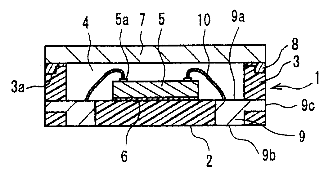
图1是表示根据本发明实施例1的固态成像装置的结构的剖面图。1 is a cross-sectional view showing the structure of a solid-state imaging device according to
图2是图1的固态成像装置的底部示意图。FIG. 2 is a schematic bottom view of the solid-state imaging device of FIG. 1 .
图3是图1的固态成像装置的侧视图。FIG. 3 is a side view of the solid-state imaging device of FIG. 1 .
图4是在没有透明板7的情况下图1的固态成像装置的顶部示意图。FIG. 4 is a schematic top view of the solid-state imaging device of FIG. 1 without the
图5A-5F是表示根据本发明实施例2的固态成像装置的制造方法的剖面图。5A-5F are cross-sectional views showing a method of manufacturing a solid-state imaging device according to
图6是这种制造方法中的引线框架的顶部示意图。Figure 6 is a top schematic view of a lead frame in this manufacturing method.
图7是其中以这种制造方法埋置引线框架的模制树脂产品的顶部示意图。Fig. 7 is a top schematic view of a molded resin product in which a lead frame is embedded in this manufacturing method.
图8A-8C是更详细示出这种制造方法的树脂模制步骤的剖面图。8A-8C are cross-sectional views illustrating the resin molding step of this manufacturing method in more detail.
图9A-9C是根据本发明实施例3的固态成像装置的制造方法的剖面图。9A-9C are cross-sectional views of a method of manufacturing a solid-state imaging device according to
图10是常规固态成像装置的剖面图。Fig. 10 is a sectional view of a conventional solid-state imaging device.
图11是表示模制这种固态成像装置的壳体的步骤的剖面图。FIG. 11 is a cross-sectional view showing a step of molding a housing of such a solid-state imaging device.
具体实施方式 Detailed ways
根据本发明的固态成像装置的结构,形成壳体的肋的上表面设有沿着外周边向下的下阶梯部分,并且用粘合剂填充这个下阶梯部分。因此,用于将透明板固定到肋的上表面的粘合剂具有足够大的体积。因而,当由热变形产生的应力作用于肋和透明板之间时,下阶梯部分的粘合剂缓解变形,并且提高了相对于应力的强度。According to the structure of the solid-state imaging device of the present invention, the upper surface of the rib forming the housing is provided with a lower stepped portion down the outer periphery, and this lower stepped portion is filled with an adhesive. Therefore, the adhesive for fixing the transparent plate to the upper surface of the rib has a sufficiently large volume. Thus, when stress due to thermal deformation acts between the rib and the transparent plate, the adhesive of the lower stepped portion relieves deformation and improves strength against stress.
优选的是,在内端部位置上的金属引线件的厚度与基座的厚度基本相等,并且外端部形成在对应内端部的位置的后表面上。还优选的是,肋的外部侧向表面形成基本上垂直于基座的表面的平面,并且透明板的端面形成得基本上与肋的外部侧向表面齐平。Preferably, the thickness of the metal lead member at the position of the inner end is substantially equal to the thickness of the base, and the outer end is formed on the rear surface at a position corresponding to the inner end. It is also preferable that the outer lateral surface of the rib forms a plane substantially perpendicular to the surface of the base, and the end surface of the transparent plate is formed substantially flush with the outer lateral surface of the rib.
根据本发明的固态成像装置的制造方法,在不增加工艺复杂性的情况下很容易制造其中用粘合剂填充下阶梯部分的结构。According to the method of manufacturing a solid-state imaging device of the present invention, the structure in which the lower stepped portion is filled with an adhesive can be easily manufactured without increasing the complexity of the process.
优选地,使用引线框架,它的形成使得它包括用于形成多个引线件的多个引线部分,并且它在对应引线部分的内端部的位置上的厚度基本上与基座的厚度相等,并且引线框架的安装使得对应引线部分的内端部的部分被夹紧在形成壳体的内部空间的下树脂模具和一部分上树脂模具之间,由此树脂模制壳体。Preferably, a lead frame is used which is formed such that it includes a plurality of lead parts for forming a plurality of lead parts, and whose thickness at positions corresponding to inner ends of the lead parts is substantially equal to the thickness of the base, And the lead frame is mounted such that a portion corresponding to an inner end portion of the lead portion is clamped between a lower resin mold forming an inner space of the case and a part of an upper resin mold, whereby the case is resin molded.
还可以在固定透明板上时将覆盖多个壳体的尺寸的透明板放在肋形成件的上表面上,并且在将肋形成件切割成单独的壳体时一起切割透明板。It is also possible to place a transparent plate of a size covering a plurality of cases on the upper surface of the rib forming member when fixing the transparent plate, and cut the transparent plates together when cutting the rib forming member into individual cases.
还可以在固定透明板时将单独透明板放在相应的壳体上,以便在肋形成件中的沟槽上的相邻透明板的边缘之间形成间隙,并且该固态成像装置被分隔在间隙区中。It is also possible to place a separate transparent plate on the corresponding housing when fixing the transparent plate so that a gap is formed between the edges of adjacent transparent plates on the groove in the rib forming member, and the solid-state imaging device is partitioned in the gap in the district.
下面参照附图详细介绍本发明的实施例。Embodiments of the present invention will be described in detail below with reference to the accompanying drawings.
实施例1Example 1
图1示出了实施例1的固态成像装置的剖面图,图2是底部示意图,图3是侧视图。FIG. 1 shows a cross-sectional view of the solid-state imaging device of
标记1表示塑料树脂(如环氧树脂)的壳体,它具有设置在平面形基座2上的矩形框架形肋3,其中平面形基座2是通过模制制造成一个部件。成像元件5通过粘合剂6固定到面对壳体1的内部空间4的基座2上。例如由玻璃制成的透明板7用粘合剂8粘接到肋3的上表面,由此密封壳体1的内部空间4并形成封装。肋3的高度设置在例如0.3到1.0mm。沿着外周边向下的下阶梯部分3a形成在肋3的上表面,并且填充到下阶梯部分3a上的粘合剂8形成厚层。在实践中,优选肋3的顶端面和下阶梯部分3a之间的阶梯差为0.05-0.5mm。
在模制期间多个金属引线件9被埋置在壳体1中。金属引线件9是用于提供从壳体1的内部空间4到外部的电引线的部件,并包括暴露在内部空间4一侧的基座2的表面上的内端部9a、暴露在与基座2后表面上的内端部9a对应的位置上的外端部9b、以及暴露在基座2的外部侧向表面的横向电极部9c。成像元件5的焊盘电极5a和金属引线件9的内端部9a由细金属线10连接。整个封装的厚度设置成例如不大于2.0mm。图4是没有透明板7的图1中的固态成像装置的平面形状的顶部示意图。A plurality of
在这种固态成像装置中,通过在肋3的上表面上形成下阶梯部分3a,下阶梯部分3a上的粘合剂8的体积可以保持足够的量。因此,当在透明板7和肋3之间由于热变形等产生应力时,下阶梯部分3a上的粘合剂8缓冲了这种变形,并且提高了相对于应力的强度。In this solid-state imaging device, by forming the lower stepped
如图1所示,对应金属引线件9的内端部9a的位置的后侧形成外端部9b。而且,在这些部分上,金属引线件9具有与基座2基本相同的厚度。因而,在树脂模制期间,可以用上、下模具夹紧内端部9a和外端部9b。因此,内端部9a的表面被上模具的表面下压并与其紧密接触,因此可以抑制树脂毛刺的产生。位于肋3下面的金属引线件9的那些部分通过半刻蚀形成得很薄,并且它们的底表面被树脂覆盖。As shown in FIG. 1 , an
如图1和3所示,壳体1的外部侧向表面即肋3的外周边表面形成基本垂直于基座2的表面的平坦表面。而且,透明板7的端面和横向电极部分9c的表面基本上与壳体1的外部侧向表面齐平。在制造工艺期间通过一起切割肋3和透明板7,可以形成这种齐平的形状并具有有利的平坦度。As shown in FIGS. 1 and 3 , the outer lateral surface of the
实施例2Example 2
下面参照图5A-5F以及图6和7介绍根据实施例2的固态成像装置的制造方法。这种制造方法用于制造具有图1所示结构的固态成像装置。A method of manufacturing the solid-state imaging device according to
首先,如图5A所示,制备引线框架21。如图6中的顶部图所示,引线框架21是其中连接多个引线部分22以便形成图1所示的金属引线件9的框架。在对应引线部分22的内端部9a的位置的厚度设置成基本上等于基座2的厚度。引线部分22具有通过半刻蚀形成在它们的底表面中的若干个凹部23,并且图1所示的金属引线件9的形状是通过在后续工艺步骤中在这个部分进行切割来实现的。First, as shown in FIG. 5A, a
接着,掩埋引线框架21,如图5B所示,由此,包括由基座24和肋25构成的多个壳体26的树脂模制产品形成在一个部件中。图7示出了模制之后的平面形状。掩埋的执行使得引线部分22的上、下表面暴露在基座24的上、下表面,形成内端部9a和外端部9b。肋形成件25具有通过将相邻壳体26的肋组合成一个而获得的形状。沟槽部分25a设置在肋形成件25的上表面上,并设置在宽度方向的中心和在纵向延伸。Next, the
接着,如图5C所示,通过粘合剂6将成像元件5固定在由肋形成件25封闭的壳体26的内部空间中,并且通过细金属线10连接成像元件5的焊盘电极5a和内端部9a。此外,粘合剂28涂敷在肋形成件25的上表面上,并且沟槽部分25a位于中心。施加的粘合剂的量稍微多于填充沟槽部分25所需的量,并设置成使得当安装透明板27时,粘合剂28的适当厚度介于沟槽部分25a的两侧的端面和透明板27之间,如后面所述的。Next, as shown in FIG. 5C, the
接着,如图5D所示,将透明板27放在其上已经施加了粘合剂28的肋形成件25的上表面上,并固定其上。Next, as shown in FIG. 5D, a
接着,如图5E所示,用切割刀29切割透明板27、肋形成件25、引线部分22和基座24,并且将其分割成若干个单独的部件,形成如图5F所示的固态成像装置。如图5E所示,切割是在垂直于24的方向在沟槽部分25a中进行的,在从上部观看时在这个方向将肋形成件25分割成两部分。结果是,构成单个固态成像装置的由透明板7制成的壳体1、基座2和肋3以及金属引线件9是通过分割的透明板27、肋形成件25、引线部分22和基座24形成的。下阶梯部分3a保持在肋3的上表面上。此外,暴露金属引线件9的横向电极部分9c。Next, as shown in FIG. 5E, the
根据本实施例的制造方法,很容易制造如下结构:其中在不使工艺复杂的情况下用粘合剂28填充下阶梯部分3a。此外,通过形成沟槽部分25a减少了肋形成件25中的树脂体积,由此减小了热收缩和膨胀。According to the manufacturing method of the present embodiment, it is easy to manufacture a structure in which the lower stepped
通过组合相邻壳体26的两个肋形成的单个肋形成件25可以设置成其宽度小于单独形成的单个肋宽度的两倍。因而,如果它如图5E所示被切割成两半,则如图5F所示的单独的固态成像装置的肋3的宽度小于单独模制的单个肋的宽度,并且固态成像装置的面积可以按这个量被收缩。A single
即使在这种情况下,肋形成件25的宽度可以保持在足够的范围内,以便涂覆用于粘接透明板27的粘合剂。在最极端的情况下,如果肋形成件25被膜制成与单独形成的肋相同的宽度,然后将它们切割成两个,则切割之后可以提供的肋3的宽度是常规肋的宽度的一半。Even in this case, the width of the
而且,当在宽度方向将肋25切割成两份时,切割面垂直于基座部分24。相反,如果像常规技术那样单独形成肋,则必须在肋的外部侧向表面上设置用于在模制之后从模具取下该装置的锥体。因而,根据本发明制造的肋的宽度减少了通过不提供锥体部分而节省的量。Also, when the
此外,由于透明板17、肋形成件25和引线部分22用相同的切割刀29一起切割,因此由透明盖27的端面、壳体1的侧向表面和金属引线件9的端面形成的封装的侧向表面基本上齐平,并且可以实现有利的平坦度。因而,当在容纳光学系统的透镜镜筒中安装该装置时,利用封装的侧面可以以高精度进行光学系统相对于成像元件5的光电检测部分的定位。就是说,通过将封装的侧表面靠着透镜镜筒的内表面,很容易相对于水平位置定位该装置。应该指出的是,通过将透镜镜筒的下表面靠着电路板表面,可以进行垂直方向的定位。In addition, since the transparent plate 17, the
参见图8A-8C,下面将更详细地介绍上述制造工艺中的如图5B所示用树脂模制壳体的工艺步骤。Referring to FIGS. 8A-8C , the process steps of molding the shell with resin as shown in FIG. 5B in the above manufacturing process will be described in more detail below.
首先,如图8A所示,将引线框架置于上模具30和下模具31之间,并且利用上模具30和下模具31夹紧引线部分22的上、下表面。下模具31的上表面是平坦的,但是在上模具30的下表面设置用于形成肋形成件25的凹部32。在凹部32的底表面中,提供用于模制沟槽部分25a的突起部30a。通过置入引线部分22,上模具30和下模具31之间形成的空间33、上模具30的凹部32的空间、和引线部分22的凹部23的空间形成用于树脂模制的空腔。First, as shown in FIG. 8A , the lead frame is placed between the
接着,如图8B所示,向空腔中填充树脂,并且模制基座24和肋形成件25。之后,打开模具,如图8C所示,取出如图5B所示的连接壳体的模制产品。Next, as shown in FIG. 8B , the cavity is filled with resin, and the
应该指出的是,还可以通过在相同平面中设置模具起模杆(ejector pin)形成沟槽部分25a,并且尺寸和尺度与突起部30a相同,从而代替在凹部32的底表面中形成突起部30a。It should be noted that instead of forming the
此外,在上述工艺中,引线部分22的上、下表面被上模具30和下模具31夹紧,确保模具表面和引线部分22的上、下表面牢固紧密接触。而且,上模具30和凹部32之间的边界位于引线部分22上方。结果是,可以有效地抑制由模制产生的树脂毛刺。In addition, in the above process, the upper and lower surfaces of the
此外,如果在模具和引线框架21之间置入用于在壳体的树脂模制期间抑制树脂突发毛刺的树脂板,可以更有效地控制毛刺的产生。Furthermore, if a resin plate for suppressing sudden burrs of the resin during resin molding of the housing is interposed between the mold and the
实施例3Example 3
下面参照图9介绍根据实施例3的制造固态成像装置的方法。这种制造方法大部分与根据实施例2的制造方法相同,但是不同于实施例2的地方在于透明板,使用单独安装的透明板来代替具有横越多个固态成像装置的区域的大表面面积的透明板。工艺的第一部分与图5A-5C所示的相同,因此省略了其说明。A method of manufacturing a solid-state imaging device according to
首先,如图9A所示,将粘合剂28涂覆到肋形成件25的上表面上,并在固定成像元件5和通过细金属线10在由肋形成件25封闭的壳体26的内部空间内完成它们的连接之后,沟槽部分25a位于中心。First, as shown in FIG. 9A, an adhesive 28 is applied to the upper surface of the
接着,如图9B所示,将透明板安装到各个壳体上。相邻透明板34的周边边缘的尺寸设置成使得在肋形成件25的上表面的沟槽部分25a内形成预定间隙。因此,通过在粘合剂28上安装透明板34,通过进入透明板34之间的间隙的粘合剂28形成嵌条35。Next, as shown in FIG. 9B, transparent plates are attached to the respective housings. The peripheral edges of the adjacent
接着,如图9C所示,用切割刀29切割嵌条35、肋形成件25、引线部分22和基座24,并将它们分成形成固态成像装置的若干件。与实施例2一样,切割是在垂直于基座24的方向在沟槽部分25a中进行的,因此当从上部观察时,将肋形成件25的宽度分成两部分。结果是,通过切割肋形成件25、引线部分22和基座24形成构成单独固态成像装置的由基座2和肋3构成的壳体1以及金属引线件9。嵌条36保留在透明板34的周边边缘上。Next, as shown in FIG. 9C, the
利用这种制造方法,即使肋25的宽度不够大,也能在透明板34的周边边缘形成嵌条36并牢固地固定透明板34。With this manufacturing method, even if the width of the
在不脱离本发明的精神或基本特性的情况下,本发明还可以以其它形式实施。本申请中公开的实施例只是示意性的而非限制性的。本发明的范围由所附权利要求书表示,而不是由前面的说明表示,并且落入权利要求书的等效性的含义和范围内的所有改变都应包含在本发明的范围内。The present invention may also be embodied in other forms without departing from the spirit or essential characteristics of the invention. The embodiments disclosed in this application are illustrative only and not restrictive. The scope of the present invention is indicated by the appended claims rather than the foregoing description, and all changes that come within the meaning and range of equivalency of the claims are intended to be embraced in the scope of the present invention.
Claims (7)
Applications Claiming Priority (2)
| Application Number | Priority Date | Filing Date | Title |
|---|---|---|---|
| JP2003311723A JP3838572B2 (en) | 2003-09-03 | 2003-09-03 | Solid-state imaging device and manufacturing method thereof |
| JP311723/2003 | 2003-09-03 |
Publications (2)
| Publication Number | Publication Date |
|---|---|
| CN1591889A CN1591889A (en) | 2005-03-09 |
| CN100433343C true CN100433343C (en) | 2008-11-12 |
Family
ID=34131846
Family Applications (1)
| Application Number | Title | Priority Date | Filing Date |
|---|---|---|---|
| CNB2004100752118A Expired - Fee Related CN100433343C (en) | 2003-09-03 | 2004-09-03 | Solid-state imaging device and manufacturing method thereof |
Country Status (5)
| Country | Link |
|---|---|
| US (2) | US7378748B2 (en) |
| EP (1) | EP1513200A3 (en) |
| JP (1) | JP3838572B2 (en) |
| KR (1) | KR100572388B1 (en) |
| CN (1) | CN100433343C (en) |
Cited By (1)
| Publication number | Priority date | Publication date | Assignee | Title |
|---|---|---|---|---|
| CN102738013A (en) * | 2011-04-13 | 2012-10-17 | 精材科技股份有限公司 | Chip package and manufacturing method thereof |
Families Citing this family (22)
| Publication number | Priority date | Publication date | Assignee | Title |
|---|---|---|---|---|
| JP2006339448A (en) * | 2005-06-02 | 2006-12-14 | Canon Inc | Exposure apparatus having a light receiving unit |
| US20070040231A1 (en) * | 2005-08-16 | 2007-02-22 | Harney Kieran P | Partially etched leadframe packages having different top and bottom topologies |
| JP4467506B2 (en) * | 2005-11-24 | 2010-05-26 | 三菱電機株式会社 | Package and electronic device using the same |
| US9711343B1 (en) * | 2006-12-14 | 2017-07-18 | Utac Thai Limited | Molded leadframe substrate semiconductor package |
| JP2008227233A (en) * | 2007-03-14 | 2008-09-25 | Matsushita Electric Ind Co Ltd | Semiconductor device manufacturing method, optical pickup module, and semiconductor device |
| JP5132957B2 (en) * | 2007-03-14 | 2013-01-30 | パナソニック株式会社 | Semiconductor device, manufacturing method thereof, and optical pickup module |
| JP2008226378A (en) * | 2007-03-14 | 2008-09-25 | Matsushita Electric Ind Co Ltd | Semiconductor device, manufacturing method thereof, and optical pickup module |
| JP2008227232A (en) * | 2007-03-14 | 2008-09-25 | Matsushita Electric Ind Co Ltd | Semiconductor device manufacturing method, semiconductor device, and optical pickup module |
| US8493748B2 (en) * | 2007-06-27 | 2013-07-23 | Stats Chippac Ltd. | Packaging system with hollow package and method for the same |
| US7763983B2 (en) * | 2007-07-02 | 2010-07-27 | Tessera, Inc. | Stackable microelectronic device carriers, stacked device carriers and methods of making the same |
| JP2009141198A (en) * | 2007-12-07 | 2009-06-25 | Panasonic Corp | Semiconductor device, manufacturing method thereof, and camera module including the semiconductor device |
| US20090152653A1 (en) * | 2007-12-14 | 2009-06-18 | Borzabadi Hamid R | Surface mount multi-axis electronics package for micro-electrical mechanical systems(MEMS) devices |
| US20100013041A1 (en) * | 2008-07-15 | 2010-01-21 | Micron Technology, Inc. | Microelectronic imager packages with covers having non-planar surface features |
| CN202523753U (en) * | 2011-10-27 | 2012-11-07 | 深圳市灏天光电有限公司 | Hidden pin high-power LED (light-emitting diode) bracket and packaging structure |
| JP5865038B2 (en) * | 2011-11-30 | 2016-02-17 | 日東電工株式会社 | ELECTRODE CONNECTION BOARD, ITS MANUFACTURING METHOD, AND LIGHT EMITTING DIODE DEVICE |
| CN116389867A (en) * | 2014-12-17 | 2023-07-04 | Lg伊诺特有限公司 | Lens driving module, camera module and optical device |
| TWI545714B (en) * | 2015-03-06 | 2016-08-11 | 矽品精密工業股份有限公司 | Electronic package and its manufacturing method |
| JP6859634B2 (en) * | 2016-09-12 | 2021-04-14 | 新日本無線株式会社 | Hollow package manufacturing method |
| FR3061628A1 (en) | 2017-01-03 | 2018-07-06 | Stmicroelectronics (Grenoble 2) Sas | METHOD FOR MANUFACTURING AN ENCAPSULATION HOOD FOR AN ELECTRONIC HOUSING AND ELECTRONIC HOUSING COMPRISING A HOOD |
| FR3061630B1 (en) | 2017-01-03 | 2021-07-09 | St Microelectronics Grenoble 2 | METHOD OF MANUFACTURING A COVER FOR AN ELECTRONIC BOX AND ELECTRONIC BOX INCLUDING A COVER |
| FR3061629A1 (en) * | 2017-01-03 | 2018-07-06 | Stmicroelectronics (Grenoble 2) Sas | METHOD FOR MANUFACTURING A HOOD FOR AN ELECTRONIC HOUSING AND ELECTRONIC HOUSING COMPRISING A HOOD |
| TWI797977B (en) * | 2022-01-27 | 2023-04-01 | 台灣晶技股份有限公司 | Package structure |
Citations (4)
| Publication number | Priority date | Publication date | Assignee | Title |
|---|---|---|---|---|
| JPS58127474A (en) * | 1982-01-25 | 1983-07-29 | Hitachi Ltd | Silid state image pickup device |
| US6384472B1 (en) * | 2000-03-24 | 2002-05-07 | Siliconware Precision Industries Co., Ltd | Leadless image sensor package structure and method for making the same |
| US6509636B1 (en) * | 2001-11-15 | 2003-01-21 | Siliconware Precision Industries Co., Ltd. | Semiconductor package |
| TW551644U (en) * | 2002-06-28 | 2003-09-01 | Cen Link Co Ltd | Electrical connector |
Family Cites Families (10)
| Publication number | Priority date | Publication date | Assignee | Title |
|---|---|---|---|---|
| JPS6428853U (en) | 1987-08-13 | 1989-02-21 | ||
| JP3074773B2 (en) | 1991-05-15 | 2000-08-07 | 日本電気株式会社 | Solid-state imaging device |
| JP2843464B2 (en) * | 1992-09-01 | 1999-01-06 | シャープ株式会社 | Solid-state imaging device |
| EP1213754A3 (en) * | 1994-03-18 | 2005-05-25 | Hitachi Chemical Co., Ltd. | Fabrication process of semiconductor package and semiconductor package |
| US6059636A (en) * | 1997-07-11 | 2000-05-09 | Tokyo Seimitsu Co., Ltd. | Wafer polishing apparatus |
| JP2001077277A (en) | 1999-09-03 | 2001-03-23 | Sony Corp | Semiconductor package and semiconductor package manufacturing method |
| TW473951B (en) * | 2001-01-17 | 2002-01-21 | Siliconware Precision Industries Co Ltd | Non-leaded quad flat image sensor package |
| JP2002373950A (en) | 2001-06-15 | 2002-12-26 | Seiko Instruments Inc | Method of manufacturing hermetically sealed IC package |
| TW551611U (en) | 2002-12-13 | 2003-09-01 | Kingpak Tech Inc | Improved structure of photo sensor package |
| JP4337668B2 (en) | 2004-07-12 | 2009-09-30 | コニカミノルタビジネステクノロジーズ株式会社 | Image forming apparatus and operation display display method |
-
2003
- 2003-09-03 JP JP2003311723A patent/JP3838572B2/en not_active Expired - Fee Related
-
2004
- 2004-08-31 US US10/931,101 patent/US7378748B2/en not_active Expired - Fee Related
- 2004-09-01 EP EP04020750A patent/EP1513200A3/en not_active Withdrawn
- 2004-09-02 KR KR1020040069915A patent/KR100572388B1/en not_active Expired - Fee Related
- 2004-09-03 CN CNB2004100752118A patent/CN100433343C/en not_active Expired - Fee Related
-
2008
- 2008-04-03 US US12/080,557 patent/US7691678B2/en not_active Expired - Fee Related
Patent Citations (4)
| Publication number | Priority date | Publication date | Assignee | Title |
|---|---|---|---|---|
| JPS58127474A (en) * | 1982-01-25 | 1983-07-29 | Hitachi Ltd | Silid state image pickup device |
| US6384472B1 (en) * | 2000-03-24 | 2002-05-07 | Siliconware Precision Industries Co., Ltd | Leadless image sensor package structure and method for making the same |
| US6509636B1 (en) * | 2001-11-15 | 2003-01-21 | Siliconware Precision Industries Co., Ltd. | Semiconductor package |
| TW551644U (en) * | 2002-06-28 | 2003-09-01 | Cen Link Co Ltd | Electrical connector |
Cited By (2)
| Publication number | Priority date | Publication date | Assignee | Title |
|---|---|---|---|---|
| CN102738013A (en) * | 2011-04-13 | 2012-10-17 | 精材科技股份有限公司 | Chip package and manufacturing method thereof |
| CN102738013B (en) * | 2011-04-13 | 2016-04-20 | 精材科技股份有限公司 | Chip package and manufacturing method thereof |
Also Published As
| Publication number | Publication date |
|---|---|
| EP1513200A2 (en) | 2005-03-09 |
| EP1513200A3 (en) | 2006-05-24 |
| CN1591889A (en) | 2005-03-09 |
| JP2005079537A (en) | 2005-03-24 |
| US7378748B2 (en) | 2008-05-27 |
| KR100572388B1 (en) | 2006-04-18 |
| KR20050024263A (en) | 2005-03-10 |
| US20080194055A1 (en) | 2008-08-14 |
| US20050044618A1 (en) | 2005-03-03 |
| US7691678B2 (en) | 2010-04-06 |
| JP3838572B2 (en) | 2006-10-25 |
Similar Documents
| Publication | Publication Date | Title |
|---|---|---|
| CN100433343C (en) | Solid-state imaging device and manufacturing method thereof | |
| CN100459136C (en) | Solid-state imaging device and manufacturing method thereof | |
| JP3782406B2 (en) | Solid-state imaging device and manufacturing method thereof | |
| CN100416816C (en) | Method for manufacturing solid-state imaging device | |
| KR100652375B1 (en) | Image sensor module structure including wire bonding package and manufacturing method thereof | |
| US7719585B2 (en) | Solid-state imaging device | |
| US8077248B2 (en) | Optical device and production method thereof | |
| JP3838571B2 (en) | Method for manufacturing solid-state imaging device | |
| JP4219943B2 (en) | Solid-state imaging device | |
| US20050109926A1 (en) | Solid-state imaging device and method for manufacturing the same | |
| JP2006332686A (en) | Solid-state imaging device |
Legal Events
| Date | Code | Title | Description |
|---|---|---|---|
| C06 | Publication | ||
| PB01 | Publication | ||
| C10 | Entry into substantive examination | ||
| SE01 | Entry into force of request for substantive examination | ||
| C14 | Grant of patent or utility model | ||
| GR01 | Patent grant | ||
| ASS | Succession or assignment of patent right |
Owner name: KELAIBO INNOVATION CO., LTD. Free format text: FORMER OWNER: MATSUSHITA ELECTRIC INDUSTRIAL CO, LTD. Effective date: 20141203 |
|
| C41 | Transfer of patent application or patent right or utility model | ||
| TR01 | Transfer of patent right |
Effective date of registration: 20141203 Address after: American California Patentee after: Craib Innovations Ltd Address before: Osaka Japan Patentee before: Matsushita Electric Industrial Co., Ltd. |
|
| CF01 | Termination of patent right due to non-payment of annual fee | ||
| CF01 | Termination of patent right due to non-payment of annual fee |
Granted publication date: 20081112 Termination date: 20160903 |