CN100479219C - Semiconductor devices having phase change memory cells, electronic systems employing the same and methods of fabricating the same - Google Patents
Semiconductor devices having phase change memory cells, electronic systems employing the same and methods of fabricating the same Download PDFInfo
- Publication number
- CN100479219C CN100479219C CNB2005100743626A CN200510074362A CN100479219C CN 100479219 C CN100479219 C CN 100479219C CN B2005100743626 A CNB2005100743626 A CN B2005100743626A CN 200510074362 A CN200510074362 A CN 200510074362A CN 100479219 C CN100479219 C CN 100479219C
- Authority
- CN
- China
- Prior art keywords
- layer
- oxidation barrier
- phase
- barrier layer
- change material
- Prior art date
- Legal status (The legal status is an assumption and is not a legal conclusion. Google has not performed a legal analysis and makes no representation as to the accuracy of the status listed.)
- Expired - Lifetime
Links
Images





Classifications
-
- H—ELECTRICITY
- H10—SEMICONDUCTOR DEVICES; ELECTRIC SOLID-STATE DEVICES NOT OTHERWISE PROVIDED FOR
- H10D—INORGANIC ELECTRIC SEMICONDUCTOR DEVICES
- H10D30/00—Field-effect transistors [FET]
- H10D30/60—Insulated-gate field-effect transistors [IGFET]
- H10D30/791—Arrangements for exerting mechanical stress on the crystal lattice of the channel regions
- H10D30/792—Arrangements for exerting mechanical stress on the crystal lattice of the channel regions comprising applied insulating layers, e.g. stress liners
-
- H—ELECTRICITY
- H10—SEMICONDUCTOR DEVICES; ELECTRIC SOLID-STATE DEVICES NOT OTHERWISE PROVIDED FOR
- H10B—ELECTRONIC MEMORY DEVICES
- H10B63/00—Resistance change memory devices, e.g. resistive RAM [ReRAM] devices
- H10B63/30—Resistance change memory devices, e.g. resistive RAM [ReRAM] devices comprising selection components having three or more electrodes, e.g. transistors
-
- H—ELECTRICITY
- H10—SEMICONDUCTOR DEVICES; ELECTRIC SOLID-STATE DEVICES NOT OTHERWISE PROVIDED FOR
- H10N—ELECTRIC SOLID-STATE DEVICES NOT OTHERWISE PROVIDED FOR
- H10N70/00—Solid-state devices having no potential barriers, and specially adapted for rectifying, amplifying, oscillating or switching
- H10N70/011—Manufacture or treatment of multistable switching devices
- H10N70/061—Shaping switching materials
-
- H—ELECTRICITY
- H10—SEMICONDUCTOR DEVICES; ELECTRIC SOLID-STATE DEVICES NOT OTHERWISE PROVIDED FOR
- H10N—ELECTRIC SOLID-STATE DEVICES NOT OTHERWISE PROVIDED FOR
- H10N70/00—Solid-state devices having no potential barriers, and specially adapted for rectifying, amplifying, oscillating or switching
- H10N70/20—Multistable switching devices, e.g. memristors
- H10N70/231—Multistable switching devices, e.g. memristors based on solid-state phase change, e.g. between amorphous and crystalline phases, Ovshinsky effect
-
- H—ELECTRICITY
- H10—SEMICONDUCTOR DEVICES; ELECTRIC SOLID-STATE DEVICES NOT OTHERWISE PROVIDED FOR
- H10N—ELECTRIC SOLID-STATE DEVICES NOT OTHERWISE PROVIDED FOR
- H10N70/00—Solid-state devices having no potential barriers, and specially adapted for rectifying, amplifying, oscillating or switching
- H10N70/801—Constructional details of multistable switching devices
- H10N70/821—Device geometry
- H10N70/826—Device geometry adapted for essentially vertical current flow, e.g. sandwich or pillar type devices
-
- H—ELECTRICITY
- H10—SEMICONDUCTOR DEVICES; ELECTRIC SOLID-STATE DEVICES NOT OTHERWISE PROVIDED FOR
- H10N—ELECTRIC SOLID-STATE DEVICES NOT OTHERWISE PROVIDED FOR
- H10N70/00—Solid-state devices having no potential barriers, and specially adapted for rectifying, amplifying, oscillating or switching
- H10N70/801—Constructional details of multistable switching devices
- H10N70/841—Electrodes
- H10N70/8413—Electrodes adapted for resistive heating
-
- H—ELECTRICITY
- H10—SEMICONDUCTOR DEVICES; ELECTRIC SOLID-STATE DEVICES NOT OTHERWISE PROVIDED FOR
- H10N—ELECTRIC SOLID-STATE DEVICES NOT OTHERWISE PROVIDED FOR
- H10N70/00—Solid-state devices having no potential barriers, and specially adapted for rectifying, amplifying, oscillating or switching
- H10N70/801—Constructional details of multistable switching devices
- H10N70/881—Switching materials
- H10N70/882—Compounds of sulfur, selenium or tellurium, e.g. chalcogenides
- H10N70/8828—Tellurides, e.g. GeSbTe
Landscapes
- Engineering & Computer Science (AREA)
- Manufacturing & Machinery (AREA)
- Semiconductor Memories (AREA)
Abstract
在一个实施例中,相变存储器件具有防止存储单元污染或氧化的氧化阻挡层及其制造方法。在一个实施例中,半导体存储器件包括覆盖在半导体衬底上的压模层。该压模层具有从其顶表面垂直扩展的突起部分。该器件进一步包括邻近突起部分的相变图案和电气连接至相变图案的下电极。
In one embodiment, a phase change memory device has an oxidation barrier layer preventing contamination or oxidation of memory cells and a method of manufacturing the same. In one embodiment, a semiconductor memory device includes a stamper layer overlying a semiconductor substrate. The stamper layer has protruding portions extending vertically from its top surface. The device further includes a phase change pattern adjacent to the protruding portion and a lower electrode electrically connected to the phase change pattern.
Description
发明背景Background of the invention
技术领域 technical field
本发明涉及一种半导体存储器件及其制造方法,具体涉及一种相变存储器件和其制造方法。The invention relates to a semiconductor storage device and a manufacturing method thereof, in particular to a phase-change storage device and a manufacturing method thereof.
背景技术 Background technique
已知用于电子存储器应用的相变材料的使用,并在例如美国专利No.6,147,395和美国专利No.6,337,266中公开。就相变存储器而言,存储器的两种状态取决于存储单元中的电流阻抗。相变材料典型地具有非晶相和晶相,分别具有固有的高和低电阻抗。非晶相存在于相对较高的温度下,晶相存在于相对低的温度下。相变存储器运行于存储单元状态(例如“接通”或“切断”)取决于温度这一基本概念之上。因此,用于设定温度高或低的装置包含在每个存储单元中。The use of phase change materials for electronic memory applications is known and disclosed, for example, in US Patent No. 6,147,395 and US Patent No. 6,337,266. In the case of phase-change memory, the two states of the memory depend on the current impedance in the memory cell. Phase change materials typically have amorphous and crystalline phases, with inherently high and low electrical impedance, respectively. The amorphous phase exists at relatively high temperatures, and the crystalline phase exists at relatively low temperatures. Phase-change memory operates on the fundamental concept that the state of a memory cell (eg, "on" or "off") depends on temperature. Therefore, means for setting the temperature high or low is included in each storage unit.
这种类型存储器的一般结构包括夹在下电极和顶电极之间的相变材料。下电极典型地起两个作用,一方面是存储单元的传导电极,另一方面是控制相变材料的相位的欧姆加热器。正如所述,该结构包括顶电极与相变材料之间、和底电极与相变材料之间的界面。在存储器件的制造过程中,和在使用中的它的使用寿命期间,这些界面可能被污染或被氧化。这种氧化引起这些界面处接触电阻的分布的巨大变化。由于相变存储器的运行取决于基于单元对电流的阻抗是“接通”或“切断”间的区分,污染或氧化危及存储器编程的准确度。仍保持对能够防止这种污染或氧化的新的相变存储结构和其制造方法的需求。The general structure of this type of memory includes a phase change material sandwiched between a bottom electrode and a top electrode. The bottom electrode typically serves two functions, on the one hand a conductive electrode for the memory cell, and on the other hand an ohmic heater controlling the phase of the phase change material. As stated, the structure includes an interface between the top electrode and the phase change material, and between the bottom electrode and the phase change material. During the fabrication of the memory device, and during its lifetime in use, these interfaces may become contaminated or oxidized. This oxidation causes large changes in the distribution of contact resistance at these interfaces. Since the operation of phase change memory depends on the distinction between being "on" or "off" based on the cell's resistance to electrical current, contamination or oxidation jeopardizes the accuracy of memory programming. There remains a need for new phase change memory structures and methods of fabrication thereof that can prevent such contamination or oxidation.
发明内容 Contents of the invention
一种相变存储器件具有防止存储单元污染或者氧化的氧化阻挡层及其制造方法。在一个实施例中,半导体存储器件包括覆盖在半导体衬底上的压模层。压模层具有从其顶表面垂直扩展的突起部分。该器件还进一步包括邻近突起部分的相变材料图案和电气连接到相变材料图案的下电极。根据本发明的一个方面,氧化阻挡层覆盖相变材料图案的侧壁与突起部分的侧壁邻接的区域。相变存储器件的更稳定运行和更长使用寿命是本发明的一些好处。A phase-change memory device has an oxidation barrier layer for preventing contamination or oxidation of memory cells and a manufacturing method thereof. In one embodiment, a semiconductor memory device includes a stamper layer overlying a semiconductor substrate. The stamper layer has protruding portions extending vertically from its top surface. The device still further includes a phase change material pattern adjacent to the protruding portion and a lower electrode electrically connected to the phase change material pattern. According to an aspect of the present invention, the oxidation barrier layer covers the region where the sidewall of the phase change material pattern adjoins the sidewall of the protrusion part. More stable operation and longer lifetime of phase change memory devices are some of the benefits of the present invention.
附图的简要说明Brief description of the drawings
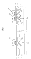
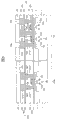
图1a是以本发明的相变存储单元阵列(CA)和周边电路区域(PCA)为特征的实施例的示意图。Figure 1a is a schematic diagram of an embodiment featuring a phase change memory cell array (CA) and peripheral circuit area (PCA) of the present invention.
图1b是根据本发明的实施例相变存储单元阵列区域和周边电路区域的一部分的平面图。FIG. 1 b is a plan view of a part of a phase-change memory cell array area and a peripheral circuit area according to an embodiment of the present invention.
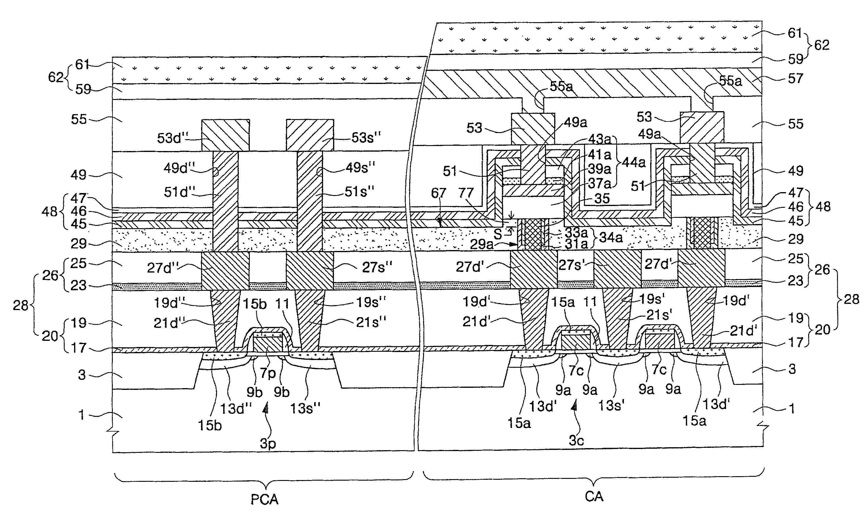
图2-9是沿显示制造本发明的实施例的工艺步骤的图1b的沿线I-I′的各剖面图。2-9 are various cross-sectional views along line I-I' of FIG. 1b showing process steps for manufacturing an embodiment of the invention.
图10是说明根据本发明的另一个实施例的相变存储器件的晶胞的剖视图。10 is a cross-sectional view illustrating a unit cell of a phase change memory device according to another embodiment of the present invention.
图11是说明根据本发明的又一个实施例的相变存储器件的晶胞的剖视图。FIG. 11 is a cross-sectional view illustrating a unit cell of a phase change memory device according to still another embodiment of the present invention.
图12是说明根据本发明的又一个的实施例的相变存储器件的晶胞的剖视图。FIG. 12 is a cross-sectional view illustrating a unit cell of a phase change memory device according to still another embodiment of the present invention.
图13是采用本发明的相变存储器件的实施例的便携式电子装置的示意性方框图。FIG. 13 is a schematic block diagram of a portable electronic device employing an embodiment of the phase change memory device of the present invention.
图14是是显示根据本发明实施例制造的相变电阻器的相变材料和下电极之间的下电极接触电阻特性的图表。14 is a graph showing the contact resistance characteristics of the lower electrode between the phase change material and the lower electrode of the phase change resistor manufactured according to an embodiment of the present invention.
图15是显示没有氧化阻挡层的传统相变存储器件的编程特性的图表。FIG. 15 is a graph showing programming characteristics of a conventional phase change memory device without an oxidation barrier layer.
图16是显示具有氧化阻挡层的本发明实施例的相变存储器件的编程特性的图表。FIG. 16 is a graph showing programming characteristics of a phase change memory device of an embodiment of the present invention having an oxidation barrier layer.
图17是说明根据本发明和传统技术制造的相变存储单元的设置/重置阻抗特性的图表。FIG. 17 is a graph illustrating the set/reset resistance characteristics of phase change memory cells manufactured according to the present invention and conventional techniques.
具体实施方式 Detailed ways
图1a是以本发明的相变存储单元阵列CA和周边电路区域PCA为特征的实施例的示意图。单元阵列区域CA包括每个依次包括存取晶体管TA和相变电阻器RP的存储单元CL的阵列。在现有技术公知的结构中,各存储单元CL连接到位线BL、字线WL、和共源极线CSL。在本发明中将包括其他传统技术,例如,周边电路区域PCA包括驱动存储单元CL的第一和第二集成电路PCA1、PCA2。存储单元CL状态由写入电流IW的电流感应确定。存储器控制的电流感应和其它功能为本领域的技术人员所知。FIG. 1 a is a schematic diagram of an embodiment featuring a phase-change memory cell array CA and a peripheral circuit area PCA of the present invention. The cell array area CA includes an array of memory cells CL each sequentially including an access transistor TA and a phase change resistor RP. In a structure known in the prior art, each memory cell CL is connected to a bit line BL, a word line WL, and a common source line CSL. Other conventional techniques will be included in the present invention, for example, the peripheral circuit area PCA includes first and second integrated circuits PCA1, PCA2 that drive memory cells CL. The state of the memory cell CL is determined by the current sensing of the write current IW. Current sensing and other functions of memory control are known to those skilled in the art.
图1b是根据本发明实施例的相变存储单元阵列区域CA的一部分和周边电路区域PCA的一部分的平面图。图1b显示单元有源区3c、共源极线27s′(在随后的图的范围内其称为″共源极衬垫27s′)、单元栅电极7c、周边栅电极7p、位线57、第一和第二源接触孔19s′和19s″、位线接触孔55a、第一和第二漏极接触孔19d′和19d″、相变电阻器44a、和相变电阻器接触孔29a。这些元件的细节将在随后说明。FIG. 1b is a plan view of a portion of a phase-change memory cell array area CA and a portion of a peripheral circuit area PCA according to an embodiment of the present invention. Figure 1b shows the cell
图2-9是沿显示制造本发明的实施例的制造步骤的图1b的线I-I′的各剖面图。Figures 2-9 are cross-sectional views along line I-I' of Figure 1b showing manufacturing steps for manufacturing an embodiment of the present invention.
参照图2,单元栅电极7c和周边的栅电极7p分别形成在单元有源区3c中的单元栅介质层5c上和周边电路有源区3p中的周边栅介质层5p上,由形成在半导体衬底1上的场隔离区3限定。单元栅电极7c和周边栅电极7p的宽度不同。优选地,周边栅电极7p的宽度至少比单元栅电极7c的宽度大大约1.5倍。而且,可以将周边栅介质层5p形成的比单元栅介质层5c厚。2, the
参照图3,形成周边电路MOS晶体管TP和单元存取MOS晶体管TA。详细地,使用单元栅电极7c作为离子注入掩模,在单元有源区3c中形成n型第一低浓度杂质区9a。此外,使用周边栅电极7p作为离子注入掩模,在周边电路有源区3p中形成p型第二低浓度杂质区9b。Referring to FIG. 3, a peripheral circuit MOS transistor TP and a cell access MOS transistor TA are formed. In detail, using the
同样,使用传统技术,沿着单元栅电极7c的相对侧以及沿着周边栅电极7p的相对侧优选形成传统的间隔材料(例如氧化物或者氮化物)的栅间隔物11。Also,
然后,使用栅间隔物11,在单元有源区3c中形成n型第一源区13s′和n型第一漏区13d′。另外,使用现有技术中公知的方法,在周边电路有源区3p中随后形成p型第二源区13s″、p型第二漏区13d″。结果,在单元区域CA中形成一对存取(开关)MOS晶体管TA,并在周边电路区域PCA中形成周边的MOS晶体管TP。Then, using the
在第二源和漏区13s″和13d″和周边栅电极7p的至少一个上形成硅化物层15b。在第一源和漏区13s′和13d′和周边单元栅电极7c的至少一个上形成硅化物层15a。然后,在最终结构上方形成低刻蚀停止层17。A
参照图4,在下刻蚀停止层17上方形成下绝缘层19,二者结合形成下中间绝缘层20。Referring to FIG. 4 , a lower insulating
其后,在单元区域CA中的下中间绝缘层20中形成第一源极接触孔19s′、第一漏极接触孔19d′。然后,使用现有技术中公知的方法,分别在第一源极接触孔19s′、第一漏极接触孔19d′中形成第一源极接触塞21s′和第一漏极接触塞21d′。同样,使用常规技术,在下中间绝缘层20中的周边电路区域PCA中形成第二源极接触孔19s″、第二漏极接触孔19d″、第二源极接触塞21s″、和第二漏极接触塞2Id″。Thereafter, a first
然后,形成上中间绝缘层26,其包括上刻蚀停止层23和上绝缘层25。元件28表示由上述的层17,19,23和25组成的中间绝缘层。Then, an upper
参照图5,在图4所示的上中间绝缘层26内形成代表图1b中共源极线27s′的横截面的共源极衬垫27s′,导电衬垫(即,第一漏极衬垫27d′)、外围电路区域源极衬垫27s″、外围电路区域漏极衬垫27d″。根据本领域技术人员公知的工艺形成这些元件。因此,共源极衬垫27s′和第一漏极衬垫27d′分别电气连接到第一源区13s′和第一漏区13d′。Referring to FIG. 5, a
然后,在最终结构上形成压模层29。然后使用光刻法和刻蚀工艺,在压模层29中形成相变电阻器接触孔29a。压模层29优选由具有高热导率的材料形成。例如,压模层29具有比二氧化硅高的热导率。除防止相变材料图案氧化的氧阻挡特性之外,这给出了相变材料图案的相变的高速淬火效率。例如,上述材料包括氮化硅和氮氧化硅。A
转向图6,共形接触间隔层34由或者一层或者两层形成。优选地,不使用氧气在真空下形成共形接触间隔层34。如果使用氧气形成共形接触间隔物层34,为了防止漏极衬垫27d氧化,优选使用较低的形成温度。共形接触间隔层34可以是使用等离子体增强(PE)CVD、或者低压(LP)CVD形成的氮化硅层。共形接触间隔层34可以由二层形成,包括在小于大约500℃以下通过使用PE-CVD形成的氮氧化硅层的下接触间隔层31、和在大于大约500℃以上通过使用LP-CVD形成的氮化硅的上接触间隔层33。Turning to FIG. 6 , the conformal
参照图7,各项异性地刻蚀共形接触间隔层34以暴露第一漏极衬垫27d′。结果,形成包括内接触间隔物31a和外接触间隔物33a的接触间隔34a。外接触间隔33a围绕内接触间隔物31a的外壁。Referring to FIG. 7, the
然后,在接触间隔物34内的相变电阻器接触孔29a中形成下电极35。然而,根据应用情况,可不需要接触间隔物34a。下电极35电气连接到第一漏极衬垫27′,其经第一接触塞2Id′依次电气连接至开关晶体管TA的第一漏区13d′。详细地,可以通过在压膜层29上和接触孔29a内沉淀导电薄膜(例如TiN膜或TiAlN膜)并通过整平导电膜直到暴露压模层29来形成相变电阻器接触孔29a中的下电极35。结果,接触间隔物34a围绕低电极35的侧壁。Then, the
其后,在包括压模层29的最终结构上顺序地形成相变材料层37、上电极层39、胶层41和硬掩模层43。硬掩模层43可以由SiO2形成。胶层41可以是例如SiN的润湿层。然而,本领域的技术人员将理解上述结构仅仅是优选实施例,还可以在本发明的精神和范围内使用其他适当的结构。例如,可以使用除了SiO2外的电介质材料形成硬掩模层43。Thereafter, a phase
相变材料层37可以由硫族化物材料形成,包括但不限于GeSbTe合金或者掺Si或者N的GeSbTe合金,具有例如大约
在图8中,可以通过构图硬掩模层43、胶层41、上电极层39、相变材料层37形成相变电阻器44a以形成硬掩模层图案43a、上电极39a、和相变材料图案37a,然后刻蚀压模层29的上部,从而与相邻的相变材料图案37a完全分离。该工艺也产生与相变电阻器44a自对准的压模层29的突起部分77。压模层29的突起部分77导致图8中所示的由符号″S″表示的表面阶梯差异。相变材料图案37a电气连接下电极35。In FIG. 8, a
然后,氧化阻挡层48覆盖包括相变电阻器44a的最终结构。氧化阻挡层48包含在小于或等于大约350℃下使用PE-CVD工艺或者原子层沉淀(ALD)工艺沉淀的单层氮化物,例如氮化硅或者氮氧化硅。可替换地,氧化阻挡层48可以由双层形成,包括在小于或等于大约350℃下使用PE-CVD工艺或者ALD工艺沉淀的氮化物的下氧化阻挡层45,例如氮化硅或者氮氧化硅;和在高于或等于大约350℃下使用PE-CVD工艺或者LP CVD工艺沉淀的氮化物的上氧化阻挡层47,例如氮化硅或者氮氧化硅。An
氧化阻挡层48防止在工艺例如覆盖相变电阻器44a的氧化物沉淀(ILD沉淀)过程中相变材料图案37a被可以深入低电极35和相变材料图案37a之间界面、或者上电极39a和相变材料图案37a之间的另一个界面的氧或者杂质氧化或者污染。The
因为氧化阻挡层48覆盖压模层29的突起部分77的侧壁、以及相变电阻器44a的侧壁和/或上表面,可以高效地阻挡氧渗透到相变电阻器44a。Because the
另外,可以在形成氧化阻挡层48之前,在小于或等于大约350℃下使用N2或者NH3在相变电阻器44a的表面上执行等离子体渗氮处理。In addition, plasma nitriding treatment may be performed on the surface of the
仍然参照图1B和8,根据本发明的另一个方面,可以通过顺序地堆积下氧化阻挡层45、应力缓冲器层46、和上氧化阻挡层47形成氧化阻挡层48。下氧化阻挡层45可以由氮化物层(例如氮氧化硅层或者氮化硅层)形成。上氧化阻挡层47可以由氮化物层,例如氮氧化硅层或者氮化硅层、或者金属氧化物层例如氧化铝层(AlO)、二氧化钛层(TiO)、氧化锆层(ZrO)、二氧化铪层(HfO)、或者氧化镧层(LaO)形成。另外,应力缓冲器层46可以由用于减轻由于氧化阻挡层47的存在而施加到下氧化阻挡层45的应力的材料层形成。例如,应力缓冲器层46由二氧化硅层形成,其在大约200至大约400℃温度下使用等离子体CVD技术形成。Still referring to FIGS. 1B and 8 , according to another aspect of the present invention, the
如果在如上所述的低于350℃的温度下形成下氧化阻挡层45,那么下氧化阻挡层45可以是多孔状。在这种情况下,由于降低了下氧化阻挡层45的氧整流效率,所以优选致密下氧化阻挡层45。使用退火技术或者等离子体处理技术执行致密处理。可以在大约400℃的温度下使用氮气或者氨气作为周围气体执行退火处理,可以在大约200至400℃的温度下使用氮气或者氨气作为等离子体源气执行等离子处理工艺。If the lower
上氧化阻挡层47可以不直接与相变材料层图案37a接触。因而,考虑到氧阻塞性能胜于施加到相变材料层图案37a的损伤,因此形成上氧化阻挡层47。也就是说,在高于形成下氧化阻挡层45的温度的温度下形成上氧化阻挡层47。例如,在比大约350℃高的温度下使用等离子体CVD技术、低压CVD技术或者原子层沉淀技术形成上氧化阻挡层47。The upper
在本发明的实施例中,上氧化阻挡层47使用原子层沉淀技术,由氧化铝层形成。在这种情况下,使用臭氧气体形成氧化铝层。臭氧气体比氧气具有更强腐蚀性。然而,由于相变材料层图案37a被下氧化阻挡层45覆盖,所以可以最小化在形成上氧化阻挡层47过程中施加到相变材料层图案37a的损伤。In an embodiment of the present invention, the upper
在本发明的另一个实施例中,可以使用溅射技术形成用作上氧化阻挡层47的金属氧化物层。在这种情况下,可以通过使用溅射技术沉淀金属层和氧化金属层已形成金属氧化层。例如,在上氧化阻挡层47由氧化铝层形成的情况下,通过使用溅射技术沉淀铝层和氧化铝层以形成氧化铝层。当使用如上所述的溅射技术和氧化处理形成氧化铝层时,将氧化铝层形成为具有相当于通过溅射处理形成的铝层厚度的一倍半的最终厚度。例如,如果用作上氧化阻挡层47的氧化铝层的最终目标厚度是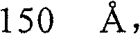
将下氧化阻挡层45形成为200至厚,将上氧化阻挡层47形成为10至厚。优选地,将下氧化阻挡层45形成为300至

其他的实施例可以省略下氧化阻挡层45的致密工艺、应力缓冲器层46的形成工艺和上氧化阻挡层47的形成工艺中的至少一个。Other embodiments may omit at least one of the densification process of the lower
图9显示图8外加下中间金属电介质(IMD)49、上电极接触孔49a、上周边源衬垫接触孔49s″、上周边漏极衬垫接触孔49d″、上电极接触塞51、周边上源塞51s″、周边上漏极塞51d″、位线衬垫53、源金属线53s″、漏极金属线53d″、上IMD 55、位线接触孔55a、和位线57的结构。根据为本领域技术人员所知的工艺添加额外元素。Fig. 9 shows Fig. 8 plus lower intermediate metal dielectric (IMD) 49, upper
然后,在最终结构上形成包括二氧化硅层59和氮化硅层61的钝化层62,以完成具有氧化阻挡层48的相变存储器件。Then, a
因此,最终存储器件包括覆盖半导体衬底1的压模层29。压模层29具有从压模层29的顶表面67垂直扩展的突起部分77。突起部分77具有至少100埃的厚度,优选地,在大约300至大约600埃的范围内。Thus, the final memory device comprises a
该存储器件还进一步包括邻近突起部分77的相变材料图案37a和电气连接到相变材料图案37a的下电极35。下电极35优选沿着其中心部分贯穿突起部分77。突起部分77位于上述第一漏极衬垫,即,导电衬垫27d′之上。另外,在本发明的精神和范围内,尽管只要相变材料图案37a邻近突起部分77,其他结构也是可能的,但相变材料图案37a覆盖突起部分77。同时,相变材料图案37a的侧壁与突起部分77的侧壁自对准。相变材料图案37a优选包括硫族化物材料例如GST(GeSbTe)合金。根据本发明的一个方面,可以用硅和氮的至少一个掺杂GST合金。The memory device further includes a phase
本器件还进一步包括电气连接至相变材料图案37a的上电极39a。The device further includes an
同样,该器件包括覆盖相变材料图案37a的侧壁的至少一部分和突起部分77的侧壁的至少一部分的氧化阻挡层48。一方面,氧化阻挡层48覆盖相变材料图案37a和上电极39a。更具体地,氧化阻挡层48优选覆盖相变材料图案37a的侧壁与突起部分77的侧壁邻接的区域,以便高效地阻塞氧渗透到相变电阻器44a。因此,用本发明的实施例,可以在本发明中形成更可靠的相变存储器件。Also, the device includes an
在本发明的另一方面,氧化阻挡层48包含覆盖上电极39a的顶端的第一部分和覆盖相变层图案37a的侧壁的第二部分。虽然没在附图中说明,但第一部分具有比第二部分的厚度更厚的厚度。优选地,第二部分的厚度大于或等于大约300埃。In another aspect of the present invention, the
图10是说明根据本发明的另一实施例的相变存储器件的晶胞的制造方法的剖视图。本实施例仅仅在下氧化阻挡层的形成方法不同于图8所述的实施例,该下氧化阻挡层对应于图8的元件45。因此,为简单起见在该实施例中仅仅描述下氧化阻挡层的形成方法。10 is a cross-sectional view illustrating a method of manufacturing a unit cell of a phase change memory device according to another embodiment of the present invention. This embodiment differs from the embodiment described in FIG. 8 only in the method of forming the lower oxidation barrier layer, which corresponds to the
参照图10,使用如参照图2至8所述相同的方法在半导体衬底1上形成相变电阻器44a。使用如参照图8所述的本质上相同的方法在具有相变电阻器44a的衬底1上形成下氧化阻挡层45。各向异性地蚀刻下氧化阻挡层45,由此在相变电阻器44a的侧壁上和在突起77的侧壁上形成具有间隔形状的下氧化阻挡层图案45a。可以使用如参照图8所述的退火工艺或者等离子体处理工艺致密化间隔形下氧化阻挡层图案45a。另外,在间隔形下氧化阻挡层图案45a上顺序地形成应力缓冲层46和上氧化阻挡层47。结果,间隔形下氧化阻挡层图案45a、应力缓冲层46、和上氧化阻挡层47组成氧化阻挡层48a。Referring to FIG. 10, a
在该实施例中,也可以省略下氧化阻挡层45a的致密处理、应力缓冲器层46的形成工艺和上氧化阻挡层47的形成工艺中的至少一个。In this embodiment, at least one of the densification process of the lower
图11是说明根据本发明的另一实施例的相变存储器件的晶胞的制造方法的剖视图。该实施例在相变材料层图案的形成方法方面与在图7和8中说明的实施例不同。11 is a cross-sectional view illustrating a method of manufacturing a unit cell of a phase change memory device according to another embodiment of the present invention. This embodiment differs from the embodiments illustrated in FIGS. 7 and 8 in the method of forming the phase change material layer pattern.
参照图11,使用如参照图2至6所述实施例的本质上相同方法在半导体衬底1上形成压模层29和接触间隔层34。如果需要接触间隔34a,各向异性刻蚀接触间隔层34以形成接触间隔34a。然后,在具有接触间隔34a的最终结构上顺序地形成相变材料层37和上电极层39,而不形成图7所示的下电极35。接着,使用如参考图7和8所述的本质上相同的方法形成相变电阻器44b和氧化阻挡层48。结果,形成每个相变电阻器44b以具有经由如图11所示的接触间隔物34a围绕的相变电阻器接触孔29a直接接触导电漏极衬垫27d′的相变材料层图案37b。也就是说,形成限制相变存储单元,即由接触间隔34a限制的相变存储单元。因此,相变材料层图案37b穿透突起部分77(参照图9)。在这种情况下,导电漏极衬垫27d′用作相变电阻器44b的下电极。Referring to FIG. 11 , the
图12是说明根据本发明的另一实施例的相变存储器件的晶胞的制造方法的剖视图。该实施例是图10和11所示实施例的组合。。12 is a cross-sectional view illustrating a method of manufacturing a unit cell of a phase change memory device according to another embodiment of the present invention. This embodiment is a combination of the embodiments shown in FIGS. 10 and 11 . .
参照图12,使用如参照图11所述本质上相同的方法在半导体衬底1上形成限制相变电阻器44b。使用如参照图10所述的本质上相同的方法在具有限制相变电阻器44b的衬底上形成氧化阻挡层48a。Referring to FIG. 12 , confinement
图13显示本发明实施例的典型应用。便携式电子装置600(例如蜂窝式电话)与处理器604和输入/输出器件606一起使用相变存储器件602。Figure 13 shows a typical application of an embodiment of the invention. Portable
图14是显示下面表1所示的四个样本A、B、C、和D的接触电阻的分布的图。FIG. 14 is a graph showing distributions of contact resistances of four samples A, B, C, and D shown in Table 1 below.

与本发明的实施例相比,样本A不包括氧化阻挡层。在图14中,容易知道样本A的接触电阻比样本B、C、和D的接触电阻具有更大的分布,其每个包括本发明的不同实施例的氧化阻挡层。In contrast to the inventive examples, Sample A does not include an oxidation barrier layer. In FIG. 14, it is easy to see that the contact resistance of Sample A has a larger distribution than that of Samples B, C, and D, each of which includes an oxidation barrier layer of a different embodiment of the present invention.
具体地,样本B包括SiON层,样本C包括SiN层,样本D包括下和上氧化阻挡层,每个都是SiN。对于样本B,在200℃下使用PECVD工艺将SiON层形成为厚。对于样本C,用与样本B相同的方法形成SiN层,对于样本D,除了在400℃下处理上层外,使用如样本B和C的方法形成两层SiN。Specifically, Sample B included a SiON layer, Sample C included a SiN layer, and Sample D included lower and upper oxidation barrier layers, each of SiN. For sample B, the SiON layer was formed using a PECVD process at 200 °C as thick. For sample C, a SiN layer was formed by the same method as sample B, and for sample D, two layers of SiN were formed using the same method as samples B and C except that the upper layer was treated at 400°C.
图14用显示均匀分布特性的样本B、C、和D的相变电阻器的下电极接触电阻来表示超过传统技术,例如样本A的改进。由本发明制造的样本中的样本D具有最稳定分布特性。FIG. 14 shows the improvement over the conventional technology, such as sample A, in terms of the lower electrode contact resistance of the phase change resistors of samples B, C, and D showing uniform distribution characteristics. Sample D among the samples produced by the present invention has the most stable distribution characteristics.
图15是显示没有氧化阻挡层的传统相变存储器件的编程特性的图表。FIG. 15 is a graph showing programming characteristics of a conventional phase change memory device without an oxidation barrier layer.
直到大约5,000编程周期,同设置的阻抗值比较起来,传统的相变存储器件具有6,000-100,000Ω的极低重置阻抗值。因此,难以得到充足的检测余量以正确地读取存储单元信息。Until about 5,000 programming cycles, conventional phase-change memory devices have extremely low reset resistance values of 6,000-100,000Ω compared to programmed resistance values. Therefore, it is difficult to obtain a sufficient detection margin to correctly read memory cell information.
图16是显示具有氧化阻挡层的本发明实施例的相变存储器件的编程特性的图表。在10个编程周期之后,与设置的阻抗值相比,根据本发明实施例的相变存储器件具有30,000-3,000,000Ω的高重置阻抗值。因而它具有很高的检测余量。FIG. 16 is a graph showing programming characteristics of a phase change memory device of an embodiment of the present invention having an oxidation barrier layer. After 10 programming cycles, the phase change memory device according to an embodiment of the present invention has a high reset resistance value of 30,000-3,000,000Ω compared to the set resistance value. Thus it has a high detection margin.
对比图15和16,可以看出充当具有氧化阻挡层的本发明的相变材料层图案的编程区域的界面区域比传统的相变材料层图案的界面区域具有更好的质量。Comparing FIGS. 15 and 16 , it can be seen that the interface region serving as the programming region of the phase change material layer pattern of the present invention with the oxidation barrier layer has better quality than that of the conventional phase change material layer pattern.
实例example
图17是说明根据本发明和常规技术制造的相变存储单元的设置/重置阻抗特性的图表。在图17中,水平轴代表相变材料图案的直径D,垂直轴代表相变电阻器的阻抗R。在图17的图表中,由参考字母″NR″和″NS″表示的数据分别代表没有氧化阻挡层制造的传统相变电阻器重置阻抗和设置阻抗。由参考字母″SR″和″SS″表示的数据分别代表由单氧化阻挡层覆盖的相变电阻器的重置阻抗和设置阻抗。另外,由参考字母″DR″和″DS″表示的数据分别代表由双氧化阻挡层覆盖的相变电阻器的重置阻抗和设置阻抗。使用下面表2所列的工艺条件制造显示图17的测量结果的相变电阻器。FIG. 17 is a graph illustrating the set/reset resistance characteristics of phase change memory cells fabricated in accordance with the present invention and conventional techniques. In FIG. 17, the horizontal axis represents the diameter D of the phase change material pattern, and the vertical axis represents the resistance R of the phase change resistor. In the graph of FIG. 17, data denoted by reference letters "NR" and "NS" represent reset resistance and set resistance, respectively, of a conventional phase change resistor fabricated without an oxidation barrier layer. Data denoted by reference letters "SR" and "SS" represent reset resistance and set resistance, respectively, of a phase change resistor covered by a single oxidation barrier layer. In addition, data denoted by reference letters "DR" and "DS" represent reset resistance and set resistance, respectively, of a phase change resistor covered by a double oxidation barrier layer. Phase change resistors showing the measured results of FIG. 17 were fabricated using the process conditions listed in Table 2 below.

参照图17和表2,随着相变材料图案的直径D的减少,逐渐地缩小了传统的相变电阻器的设置阻抗和重置阻抗之间的差异。例如,当相变材料图案的直径D从0.68μm减少到0.4μm时,传统的相变电阻器的重置/设置阻抗比突然地从大约1.6×102减少到大约0.5×10。另外,具有0.4μm直径的相变材料图案的传统的相变电阻器显示大约6×104至大约7×105的不均匀设置阻抗。Referring to FIG. 17 and Table 2, as the diameter D of the phase change material pattern decreases, the difference between the set resistance and the reset resistance of the conventional phase change resistor is gradually reduced. For example, when the diameter D of the phase-change material pattern is reduced from 0.68 μm to 0.4 μm, the reset/set resistance ratio of conventional phase-change resistors suddenly decreases from about 1.6×10 2 to about 0.5×10 . In addition, a conventional phase change resistor having a phase change material pattern with a diameter of 0.4 μm shows a non-uniform setting resistance of about 6×10 4 to about 7×10 5 .
另一方面,当相变材料图案的直径D从0.68μm减少到0.4μm时,用单氧化阻挡层覆盖的相变电阻器的重置/设置阻抗比从大约1.6×102减少到大约1×102。另外,当相变材料图案的直径D从0.68μm减少到0.4μm时,用双氧化阻挡层覆盖的相变电阻器的重置/设置阻抗比从大约2.5×102减少到大约1.3×102。特别地,与具有0.4μm直径的相变材料图案的传统的相变电阻器相比,用单氧化阻挡层或者双氧化阻挡层覆盖并具有0.4μm的直径的相变材料图案的相变电阻器显示更均一的设置阻抗。On the other hand, when the diameter D of the phase-change material pattern is reduced from 0.68 μm to 0.4 μm, the reset/set resistance ratio of the phase-change resistor covered with a single oxidation barrier layer is reduced from about 1.6× 10 to about 1× 10 2 . In addition, when the diameter D of the phase-change material pattern is reduced from 0.68 μm to 0.4 μm, the reset/set resistance ratio of the phase-change resistor covered with the double oxidation barrier layer is reduced from about 2.5×10 2 to about 1.3×10 2 . In particular, compared with a conventional phase change resistor having a phase change material pattern with a diameter of 0.4 μm, a phase change resistor covered with a single oxidation barrier layer or a double oxidation barrier layer and having a phase change material pattern with a diameter of 0.4 μm Shows a more uniform setup impedance.
尽管参照优选实施例描述本发明,应理解本发明不局限于其中的细节。在前面的描述中已经提出了多种置换和修改,本领域的技术人员可以想到其他的。因此,所有的置换和修改均包含在所附权利要求限定的本发明的范围内。Although the invention has been described with reference to preferred embodiments, it should be understood that the invention is not limited to the details therein. Various permutations and modifications have been suggested in the foregoing description, and others will occur to those skilled in the art. Accordingly, all permutations and modifications are included within the scope of the present invention as defined by the appended claims.
Claims (85)
Applications Claiming Priority (4)
| Application Number | Priority Date | Filing Date | Title |
|---|---|---|---|
| KR20040037965 | 2004-05-27 | ||
| KR1020040037965 | 2004-05-27 | ||
| KR1020040105905 | 2004-12-14 | ||
| KR1020050031662 | 2005-04-15 |
Publications (2)
| Publication Number | Publication Date |
|---|---|
| CN1702883A CN1702883A (en) | 2005-11-30 |
| CN100479219C true CN100479219C (en) | 2009-04-15 |
Family
ID=35424233
Family Applications (1)
| Application Number | Title | Priority Date | Filing Date |
|---|---|---|---|
| CNB2005100743626A Expired - Lifetime CN100479219C (en) | 2004-05-27 | 2005-05-27 | Semiconductor devices having phase change memory cells, electronic systems employing the same and methods of fabricating the same |
Country Status (2)
| Country | Link |
|---|---|
| US (1) | US7411208B2 (en) |
| CN (1) | CN100479219C (en) |
Families Citing this family (43)
| Publication number | Priority date | Publication date | Assignee | Title |
|---|---|---|---|---|
| CN101834198A (en) | 2004-05-14 | 2010-09-15 | 瑞萨电子株式会社 | Semiconductor memory device |
| KR100615598B1 (en) * | 2004-07-19 | 2006-08-25 | 삼성전자주식회사 | Semiconductor devices having planarization insulating film and methods of forming the same |
| KR100652378B1 (en) * | 2004-09-08 | 2006-12-01 | 삼성전자주식회사 | Antimony precursor and manufacturing method of phase change memory device using same |
| US20060169968A1 (en) * | 2005-02-01 | 2006-08-03 | Thomas Happ | Pillar phase change memory cell |
| JP2006278864A (en) * | 2005-03-30 | 2006-10-12 | Renesas Technology Corp | Phase change non-volatile memory and its manufacturing method |
| KR100701693B1 (en) * | 2005-05-26 | 2007-03-29 | 주식회사 하이닉스반도체 | Phase change memory device and manufacturing method thereof |
| US20060289848A1 (en) * | 2005-06-28 | 2006-12-28 | Dennison Charles H | Reducing oxidation of phase change memory electrodes |
| JP2007019305A (en) * | 2005-07-08 | 2007-01-25 | Elpida Memory Inc | Semiconductor memory device |
| US20070023857A1 (en) * | 2005-07-29 | 2007-02-01 | Ming Jin | Fabricating sub-lithographic contacts |
| US7362608B2 (en) * | 2006-03-02 | 2008-04-22 | Infineon Technologies Ag | Phase change memory fabricated using self-aligned processing |
| US7495946B2 (en) | 2006-03-02 | 2009-02-24 | Infineon Technologies Ag | Phase change memory fabricated using self-aligned processing |
| US7324365B2 (en) | 2006-03-02 | 2008-01-29 | Infineon Technologies Ag | Phase change memory fabricated using self-aligned processing |
| US20070215987A1 (en) * | 2006-03-15 | 2007-09-20 | Schwerin Ulrike G | Method for forming a memory device and memory device |
| CN100563971C (en) * | 2006-04-14 | 2009-12-02 | 浙江工业大学 | Composite materials for saw blades |
| CN100492695C (en) * | 2006-05-26 | 2009-05-27 | 中国科学院上海微系统与信息技术研究所 | Method for preparing phase change memory by silicon wet etching and bonding process |
| JP4865433B2 (en) * | 2006-07-12 | 2012-02-01 | ルネサスエレクトロニクス株式会社 | Semiconductor device and manufacturing method thereof |
| CN100530738C (en) * | 2006-08-24 | 2009-08-19 | 财团法人工业技术研究院 | Phase change memory cell structure and manufacturing method thereof |
| JP2008091703A (en) * | 2006-10-03 | 2008-04-17 | Toshiba Corp | Semiconductor memory device |
| US7593254B2 (en) * | 2007-05-25 | 2009-09-22 | Micron Technology, Inc. | Variable resistance memory device with an interfacial adhesion heating layer, systems using the same and methods of forming the same |
| US8344349B2 (en) * | 2007-09-07 | 2013-01-01 | Taiwan Semiconductor Manufacturing Co., Ltd. | Electronic component, and a method of manufacturing an electronic component |
| KR100951661B1 (en) | 2008-03-27 | 2010-04-07 | 주식회사 하이닉스반도체 | Phase change memory device having a protective film to protect the phase change material and manufacturing method thereof |
| KR100976796B1 (en) * | 2008-06-03 | 2010-08-20 | 주식회사 동부하이텍 | Nonvolatile Semiconductor Memory Device and Manufacturing Method Thereof |
| US20100314690A1 (en) * | 2009-06-15 | 2010-12-16 | Taiwan Semiconductor Manufacturing Company, Ltd. | Sidewall-Free CESL for Enlarging ILD Gap-Fill Window |
| CN102332530B (en) * | 2010-07-13 | 2013-08-14 | 中国科学院上海微系统与信息技术研究所 | Memory cell with spacer heating electrode and phase change material and preparation method |
| CN102142517B (en) * | 2010-12-17 | 2017-02-08 | 华中科技大学 | Multiple-layer phase-change material with low thermal conductivity |
| CN102544358B (en) * | 2010-12-27 | 2014-02-05 | 中芯国际集成电路制造(北京)有限公司 | Phase change memory and preparation method thereof |
| CN102569648B (en) * | 2010-12-27 | 2014-09-03 | 中芯国际集成电路制造(北京)有限公司 | Phase change memory and manufacturing method thereof |
| US9673102B2 (en) * | 2011-04-01 | 2017-06-06 | Micron Technology, Inc. | Methods of forming vertical field-effect transistor with self-aligned contacts for memory devices with planar periphery/array and intermediate structures formed thereby |
| JP2012248814A (en) * | 2011-05-31 | 2012-12-13 | Toshiba Corp | Semiconductor device and manufacturing method of the same |
| US8853665B2 (en) | 2012-07-18 | 2014-10-07 | Micron Technology, Inc. | Semiconductor constructions, memory cells, memory arrays and methods of forming memory cells |
| CN104051617B (en) * | 2013-03-15 | 2017-05-10 | 台湾积体电路制造股份有限公司 | Resistance variable memory structure and method of forming the same |
| US9349953B2 (en) * | 2013-03-15 | 2016-05-24 | Taiwan Semiconductor Manufacturing Company, Ltd. | Resistance variable memory structure and method of forming the same |
| US9166159B2 (en) | 2013-05-23 | 2015-10-20 | Micron Technology, Inc. | Semiconductor constructions and methods of forming memory cells |
| US9397143B2 (en) * | 2013-12-20 | 2016-07-19 | Intel Corporation | Liner for phase change memory (PCM) array and associated techniques and configurations |
| JP2016072538A (en) * | 2014-09-30 | 2016-05-09 | 株式会社東芝 | Storage device and manufacturing method thereof |
| CN104867864B (en) * | 2015-03-27 | 2018-08-28 | 上海新储集成电路有限公司 | A method of realizing local interlinkage |
| KR102641744B1 (en) * | 2017-01-20 | 2024-03-04 | 삼성전자주식회사 | Variable resistance memory device |
| KR102550099B1 (en) | 2018-08-23 | 2023-06-30 | 삼성전자주식회사 | Variable resistance memory devices |
| CN111933796B (en) * | 2020-09-29 | 2020-12-18 | 杭州未名信科科技有限公司 | A kind of resistive memory and its manufacturing method |
| US11456415B2 (en) * | 2020-12-08 | 2022-09-27 | International Business Machines Corporation | Phase change memory cell with a wrap around and ring type of electrode contact and a projection liner |
| US11476418B2 (en) | 2020-12-08 | 2022-10-18 | International Business Machines Corporation | Phase change memory cell with a projection liner |
| TWI813965B (en) | 2021-03-17 | 2023-09-01 | 華邦電子股份有限公司 | Semiconductor device and method of forming the same |
| FR3125917B1 (en) * | 2021-07-30 | 2023-08-04 | St Microelectronics Crolles 2 Sas | Phase change memory |
Citations (3)
| Publication number | Priority date | Publication date | Assignee | Title |
|---|---|---|---|---|
| US4115872A (en) * | 1977-05-31 | 1978-09-19 | Burroughs Corporation | Amorphous semiconductor memory device for employment in an electrically alterable read-only memory |
| US4499557A (en) * | 1980-10-28 | 1985-02-12 | Energy Conversion Devices, Inc. | Programmable cell for use in programmable electronic arrays |
| US4599705A (en) * | 1979-12-13 | 1986-07-08 | Energy Conversion Devices, Inc. | Programmable cell for use in programmable electronic arrays |
Family Cites Families (20)
| Publication number | Priority date | Publication date | Assignee | Title |
|---|---|---|---|---|
| US209746A (en) * | 1878-11-12 | Improvement in paper-tube machines | ||
| FR2478879A1 (en) * | 1980-03-24 | 1981-09-25 | Commissariat Energie Atomique | METHOD FOR MAKING AMORPHOUS SEMICONDUCTOR MEMORY EFFECT DEVICES |
| US5177567A (en) * | 1991-07-19 | 1993-01-05 | Energy Conversion Devices, Inc. | Thin-film structure for chalcogenide electrical switching devices and process therefor |
| US6337266B1 (en) * | 1996-07-22 | 2002-01-08 | Micron Technology, Inc. | Small electrode for chalcogenide memories |
| US6147395A (en) * | 1996-10-02 | 2000-11-14 | Micron Technology, Inc. | Method for fabricating a small area of contact between electrodes |
| US5952671A (en) * | 1997-05-09 | 1999-09-14 | Micron Technology, Inc. | Small electrode for a chalcogenide switching device and method for fabricating same |
| US6031287A (en) * | 1997-06-18 | 2000-02-29 | Micron Technology, Inc. | Contact structure and memory element incorporating the same |
| US6642102B2 (en) * | 2001-06-30 | 2003-11-04 | Intel Corporation | Barrier material encapsulation of programmable material |
| EP1318552A1 (en) * | 2001-12-05 | 2003-06-11 | STMicroelectronics S.r.l. | Small area contact region, high efficiency phase change memory cell and fabrication method thereof |
| US6891747B2 (en) * | 2002-02-20 | 2005-05-10 | Stmicroelectronics S.R.L. | Phase change memory cell and manufacturing method thereof using minitrenches |
| JP3999549B2 (en) | 2002-04-01 | 2007-10-31 | 株式会社リコー | Phase change material element and semiconductor memory |
| US6858482B2 (en) * | 2002-04-10 | 2005-02-22 | Micron Technology, Inc. | Method of manufacture of programmable switching circuits and memory cells employing a glass layer |
| KR20030081900A (en) | 2002-04-15 | 2003-10-22 | 삼성전자주식회사 | Method of fabricating Phase change Memory device |
| KR100437458B1 (en) | 2002-05-07 | 2004-06-23 | 삼성전자주식회사 | Phase change memory cells and methods of fabricating the same |
| KR100448908B1 (en) | 2002-09-03 | 2004-09-16 | 삼성전자주식회사 | Phase-changeable memory device structure and method for fabricating the same |
| KR100481865B1 (en) * | 2002-11-01 | 2005-04-11 | 삼성전자주식회사 | Phase changeable memory device and method of fabricating the same |
| US6744088B1 (en) | 2002-12-13 | 2004-06-01 | Intel Corporation | Phase change memory device on a planar composite layer |
| KR100560659B1 (en) * | 2003-03-21 | 2006-03-16 | 삼성전자주식회사 | Phase change memory device and manufacturing method thereof |
| KR100564608B1 (en) * | 2004-01-29 | 2006-03-28 | 삼성전자주식회사 | Phase change memory device |
| US7482616B2 (en) * | 2004-05-27 | 2009-01-27 | Samsung Electronics Co., Ltd. | Semiconductor devices having phase change memory cells, electronic systems employing the same and methods of fabricating the same |
-
2004
- 2004-12-30 US US11/027,255 patent/US7411208B2/en not_active Expired - Lifetime
-
2005
- 2005-05-27 CN CNB2005100743626A patent/CN100479219C/en not_active Expired - Lifetime
Patent Citations (3)
| Publication number | Priority date | Publication date | Assignee | Title |
|---|---|---|---|---|
| US4115872A (en) * | 1977-05-31 | 1978-09-19 | Burroughs Corporation | Amorphous semiconductor memory device for employment in an electrically alterable read-only memory |
| US4599705A (en) * | 1979-12-13 | 1986-07-08 | Energy Conversion Devices, Inc. | Programmable cell for use in programmable electronic arrays |
| US4499557A (en) * | 1980-10-28 | 1985-02-12 | Energy Conversion Devices, Inc. | Programmable cell for use in programmable electronic arrays |
Non-Patent Citations (1)
| Title |
|---|
| Ge-Sb-Te-O相变薄膜的光学性质研究. 顾四朋,候立松,曾贤成,赵启涛.光学仪器,第23卷第5-6期. 2001 * |
Also Published As
| Publication number | Publication date |
|---|---|
| US20050263823A1 (en) | 2005-12-01 |
| CN1702883A (en) | 2005-11-30 |
| US7411208B2 (en) | 2008-08-12 |
Similar Documents
| Publication | Publication Date | Title |
|---|---|---|
| CN100479219C (en) | Semiconductor devices having phase change memory cells, electronic systems employing the same and methods of fabricating the same | |
| US8026543B2 (en) | Semiconductor devices having phase change memory cells, electronic systems employing the same and methods of fabricating the same | |
| CN1288744C (en) | Method of fabricating 1t1r resistive memory array | |
| KR101598716B1 (en) | Top electrode blocking layer for rram device | |
| US10256272B2 (en) | Resistive memory device containing etch stop structures for vertical bit line formation and method of making thereof | |
| US10121965B1 (en) | Resistive random access memory device containing discrete memory material portions and method of making thereof | |
| JP5143349B2 (en) | Method for manufacturing intersection non-volatile memory element employing binary metal oxide film as data storage material film | |
| CN111180445B (en) | Ferroelectric memory and method of manufacturing the same | |
| TWI398954B (en) | Variable and reversible resistive element, non-volatile memory unit, method of operation thereof, and method of manufacture | |
| US10096654B2 (en) | Three-dimensional resistive random access memory containing self-aligned memory elements | |
| TWI775049B (en) | Non-volatile memory device and manufacturing method thereof | |
| US20050263801A1 (en) | Phase-change memory device having a barrier layer and manufacturing method | |
| TW202018917A (en) | Non-volatile memory and manufacturing method thereof | |
| TW201411814A (en) | Resistance memory cell, resistance memory array and method of forming the same | |
| KR102661235B1 (en) | Data storage element and manufacturing method thereof | |
| JP2008294103A (en) | Resistance change memory and manufacturing method thereof | |
| JP2005340837A (en) | Semiconductor device having phase change memory element covered with oxygen barrier film, electronic system using the same, and method of manufacturing the same | |
| US7932509B2 (en) | Phase change memory element | |
| KR100519240B1 (en) | Manufacturing method of capacitor electrode made of platinum metal | |
| JP2005268288A (en) | Semiconductor device and manufacturing method thereof | |
| KR100675278B1 (en) | Semiconductor devices having phase change memory cells covered with an oxygen barrier film, electronic systems employing them and methods of manufacturing the same | |
| JP3627814B2 (en) | Structure of capacitor for integrated circuit and manufacturing method thereof | |
| TWI860482B (en) | Resistive random access memory and manufacturing method thereof | |
| CN104810474A (en) | Resistive element and memory cell of nonvolatile memory and related manufacturing method thereof | |
| TW200913166A (en) | Non-volatile memory and manufacturing method thereof |
Legal Events
| Date | Code | Title | Description |
|---|---|---|---|
| C06 | Publication | ||
| PB01 | Publication | ||
| C10 | Entry into substantive examination | ||
| SE01 | Entry into force of request for substantive examination | ||
| C14 | Grant of patent or utility model | ||
| GR01 | Patent grant | ||
| CX01 | Expiry of patent term |
Granted publication date: 20090415 |
|
| CX01 | Expiry of patent term |