Semiconductor interconnect structure and NOR type fast flash memory bank and manufacture method thereof
Technical field
The present invention relates to a kind of semiconductor interconnect structure and NOR type fast flash memory bank (NOR-typeflash memory), and particularly relevant for a kind of semiconductor interconnect structure and NOR type fast flash memory bank that dwindles spacing.
Background technology
Fig. 1 is the vertical view of known a kind of NOR type fast flash memory bank, and Fig. 2 is the generalized section of the II-II ' line of Fig. 1.
Please consult Fig. 1 and Fig. 2 simultaneously, in a substrate 100, have with staggered diffusion region 102 of Y direction and isolated area 104, and in substrate 100, have with the spaced control grid 106 of directions X.Float gate (not shown) and tunnel oxide (not shown) in the memory cell then is to be arranged in the zone 110 that each diffusion region 102 and control grid 106 change mutually.In addition, 102 of diffusion regions that can be used as source area 108a, opposite side in the diffusion region 102 of control grid 106 1 sides can be used as drain area 108b.And the drain area 108b with delegation is external to a lead (not shown) by a plurality of contact holes 112 usually.Compare down, with the source area 108a of delegation then as shown in Figure 2, it is the isolation structure of removing earlier among the source area 108a (that is isolated area 104), form the source area 108a that doped region 114 connects with delegation again in the substrate 100 that in source area 108a, is exposed, last pick up line (source pickup line) 116 via the one source pole that is arranged on 104 of two isolated areas again and contact hole 118 wherein is external to a lead (not shown), source area 108a is electrically conducted.
Yet, because said structure uses a lot of contact holes, and make the area of NOR type fast flash memory bank further to dwindle, and semiconductor is disagreed at present toward the trend of miniaturization development.In addition, its external lead can increase the size of NOR shape fast flash memory bank body.
Summary of the invention
Purpose of the present invention is providing a kind of semiconductor interconnect structure exactly, to obtain less semiconductor element.
A further object of the present invention provides a kind of manufacture method of semiconductor interconnect structure, to improve the integration of semiconductor element.
Another purpose of the present invention provides a kind of manufacture method of NOR type fast flash memory bank, to obtain less memory body area
Another object of the present invention provides a kind of manufacture method of NOR type fast flash memory bank, with reduction memory body area.
The present invention proposes a kind of semiconductor interconnect structure, comprises a substrate, an isolation structure and a conducting block.Wherein, in this substrate, be formed with irrigation canals and ditches, and isolation structure is disposed in the irrigation canals and ditches and comprise a conductor layer, conductor layer to be disposed in the isolation structure and do not contact with the irrigation canals and ditches surface.Conducting block is arranged in irrigation canals and ditches, and electrically connects with conductor layer, and wherein the upper surface of the upper surface of conducting block and substrate is a copline.
Described according to a preferred embodiment of the present invention, in above-mentioned semiconductor interconnect structure, the material of insulating barrier comprises silica.
Described according to a preferred embodiment of the present invention, in above-mentioned semiconductor interconnect structure, the material of conductor layer comprises doped polycrystalline silicon.
The present invention proposes a kind of manufacture method of semiconductor interconnect structure, and a substrate at first is provided, and has been formed with irrigation canals and ditches in substrate.Then, form one deck lining oxide layer on the surface of irrigation canals and ditches.Then, form one deck conductor layer on the lining oxide layer in irrigation canals and ditches, and the upper surface of conductor layer is lower than the upper surface of substrate.Form an oxide layer and fill up irrigation canals and ditches in irrigation canals and ditches, oxide layer and lining oxide layer form an isolation structure.Remove isolation structure partly to expose conductor layer.Next, in irrigation canals and ditches, form a conducting block, and conducting block and conductor layer electric connection, wherein the upper surface of the upper surface of conducting block and substrate is a copline.
Described according to a preferred embodiment of the present invention, in the manufacture method of above-mentioned semiconductor interconnect structure, form the method for one deck lining oxide layer on the surface of irrigation canals and ditches, at first in substrate, form one deck patterning cover curtain layer.Then, a thermal oxidation processing procedure is carried out in substrate.Then, remove the patterning cover curtain layer.
Described according to a preferred embodiment of the present invention, in the manufacture method of above-mentioned semiconductor interconnect structure, the method that forms conformal one deck layer of oxide material in substrate comprises chemical vapour deposition technique.
Described according to a preferred embodiment of the present invention, in the manufacture method of above-mentioned semiconductor interconnect structure, form the method for one deck conductor layer on the lining oxide layer in irrigation canals and ditches, for prior to forming one deck patterning cover curtain layer in the substrate.Afterwards, a thermal oxidation processing procedure is carried out in substrate.Next, remove the patterning cover curtain layer.
The present invention proposes a kind of NOR type fast flash memory bank, comprises a substrate, most bar control grid, most bar irrigation canals and ditches, most bar source area, most bar drain area, most individual isolation structure, most conducting blocks, most the gates of floating, a majority tunnel oxide and dielectric layers.Wherein, these control grids are arranged in the substrate with a first direction, and these irrigation canals and ditches are arranged in substrate surface with a second direction.Moreover these source areas are positioned at the substrate between these irrigation canals and ditches of a side of each control grid.And these drain areas lay respectively in the substrate between these irrigation canals and ditches of opposite side of each control grid.Each isolation structure is disposed in those irrigation canals and ditches, and comprises one deck conductor layer, and wherein the part of isolation structure exposes each conductor layer, and each conductor layer in another part of isolation structure is coated by each isolation structure.In addition, these conducting blocks lay respectively in these irrigation canals and ditches between adjacent two source areas, and fill up these irrigation canals and ditches, and electrically connect with these source areas and these conductor layers, wherein the upper surface of the upper surface of conducting block and substrate is a copline, and floats gate between the substrate and these control grids between these source areas and these drain areas.These tunnel oxides are floated between gate and the substrate at these, and dielectric layer is floated between gate and these control grids at these.
Described according to a preferred embodiment of the present invention, the NOR type fast flash memory bank above-mentioned more comprises plurality of wires, electrically connects each drain area respectively.
Described according to a preferred embodiment of the present invention, in above-mentioned NOR type fast flash memory bank, the material of these conductor layers comprises doped polycrystalline silicon.
The present invention proposes a kind of manufacture method of NOR type fast flash memory bank, at first is provided with most bar source areas and the most bar drain area of arranging with a first direction in a substrate, forms most bar irrigation canals and ditches of arranging with a second direction in substrate surface again.Then, in these irrigation canals and ditches, form most bar isolation structures, and be separated out most active regions, and the formation method of each isolation structure, for the surface prior to each irrigation canals and ditches forms one deck lining oxide layer, then formation one deck conductor layer on the lining oxide layer in each irrigation canals and ditches, and the upper surface of conductor layer is lower than the upper surface of substrate, forms a layer insulating again on the conductor layer in irrigation canals and ditches and fills up this irrigation canals and ditches.Then, form most tunnel oxides and most the gates of floating in these source areas in these active regions and the substrate between these drain areas in regular turn.Next, in substrate, form the one dielectric layer that covers these gates of floating, between these source areas and these drain areas, form most bar control grids again.Afterwards, remove the isolation structure of a part in these irrigation canals and ditches of these source areas, to expose these conductor layers.Continue it, form most conducting blocks in these irrigation canals and ditches in these source areas, fill up these irrigation canals and ditches respectively, and electrically connect with source area and conductor layer, wherein the upper surface of the upper surface of conducting block and substrate is a copline.Subsequently, form most doped regions in the substrate that exposes in these source areas and these drain areas, wherein these doped regions in these source areas are electrical connected by these conducting blocks.
Described according to a preferred embodiment of the present invention, in the manufacture method of above-mentioned NOR type fast flash memory bank, form the method for lining oxide layer on the surface of irrigation canals and ditches, for prior to forming one deck patterning cover curtain layer in the substrate.Afterwards, a thermal oxidation processing procedure is carried out in substrate.Next, remove the patterning cover curtain layer.
Described according to a preferred embodiment of the present invention, in the manufacture method of above-mentioned NOR type fast flash memory bank, form the method for these conductor layers on these lining oxide layers in these irrigation canals and ditches, for prior to forming one deck conductor material layer in the substrate and filling up irrigation canals and ditches.Then, remove part conductor material layer in suprabasil conductor material layer and these irrigation canals and ditches.
Described according to a preferred embodiment of the present invention, in the manufacture method of above-mentioned NOR type fast flash memory bank, the method that forms conductor material layer in substrate comprises chemical vapour deposition technique.
Described according to a preferred embodiment of the present invention, in the manufacture method of above-mentioned NOR type fast flash memory bank, the formation method of these conducting blocks is for prior to forming the layer of conductive material layer and filling up these irrigation canals and ditches in the source area in the substrate.Then, remove the conductive material layer of substrate top.
Described according to a preferred embodiment of the present invention, in the manufacture method of above-mentioned NOR type fast flash memory bank, the formation method of these doped regions comprises ionic-implantation.
Described according to a preferred embodiment of the present invention, in the manufacture method of above-mentioned NOR type fast flash memory bank, form after these control grids, more be included in and form plurality of wires in the substrate, and each lead is electrically connected at each drain area respectively.
The present invention can obtain less semiconductor element because of being used in the semiconductor interconnect that forms in the isolation structure, as partly to lead the contact structure that intraconnections can replace known connection memory body source area among the present invention, therefore can obtain less memory body area.
On the other hand, in NOR type fast flash memory bank proposed by the invention, the source electrode that does not need to form in the known techniques is picked up line, therefore can further dwindle the memory body area.
In addition,, the processing procedure of isolation structure and the difficult line of semiconductor is integrated, can in the time of reduction memory body area, be simplified processing procedure and reduce manufacturing cost by the variation on the processing procedure.
For above-mentioned and other purposes, feature and advantage of the present invention can be become apparent, preferred embodiment cited below particularly, and cooperate appended graphicly, be described in detail below.
Description of drawings
Fig. 1 is the vertical view of known a kind of NOR type fast flash memory bank.
Fig. 2 is the generalized section of the II-II ' line of Fig. 1.
Fig. 3 is the generalized section of a kind of semiconductor interconnect of illustrating according to the first embodiment of the present invention.
Fig. 4 A~Fig. 4 D is the manufacturing process profile of a kind of semiconductor interconnect of illustrating according to the second embodiment of the present invention.
Fig. 5 A is the vertical view according to a kind of NOR type fast flash memory bank of the first embodiment of the present invention.
Fig. 5 B is the generalized section of the B-B ' line of Fig. 5 A.
Fig. 5 C is the generalized section of the C-C ' line of Fig. 5 A.
Fig. 6 A~Fig. 6 G is the manufacturing process profile according to the NOR type fast flash memory bank of the second embodiment of the present invention.
100,300,400,500,600: substrate 102: diffusion region
104: isolated area 106,502,622: control grid
108a, 506: source area 108b, 508: drain area
110: zone 112,118: contact hole
114,630: doped region 116: source electrode is picked up line
302,406,504,606: irrigation canals and ditches 304: insulating barrier
306,412,512,614: conductor layer 402,602: pad oxide
404,604,624: patterning cover curtain layer 408: lining oxide layer
410: conductor material layer 414: layer of oxide material
416: oxide layer 504: control grid
510,608: isolation structure 514,626: conducting block
516,618: the gate 518,616 of floating: tunneling oxide layer
520,612,620: dielectric layer 610: active region
628: conductor material layer
Embodiment
First embodiment
Seeing also shown in Figure 3ly, is the generalized section of a kind of semiconductor interconnect of illustrating according to the first embodiment of the present invention.See also Fig. 3, semiconductor interconnect comprises substrate 300, insulating barrier 304 and conductor layer 306.Wherein, be formed with irrigation canals and ditches 302 in this substrate 300, and insulating barrier 304 is disposed in the irrigation canals and ditches 302, its material for example is a silica.Moreover conductor layer 306 is disposed in the insulating barrier 304, and is insulated 304 coating of layer, and its material for example is a doped polycrystalline silicon.
Because the semiconductor interconnect among first embodiment, conductor layer 306 is to be disposed in the insulating barrier 304, can effectively save the space, to reduce the size of semiconductor element.
Second embodiment
Seeing also shown in Fig. 4 A~Fig. 4 C, is the manufacturing process profile of a kind of semiconductor interconnect of illustrating according to the second embodiment of the present invention.At first, see also Fig. 4 A, a substrate 400 at first is provided, be formed with irrigation canals and ditches 406 in substrate 400, its formation method for example is prior to forming a patterning cover curtain layer 404 in the substrate 400, then carries out an etch process again and forms it.Wherein, the material of patterning cover curtain layer 404 for example is a silicon nitride.In addition, can before formation patterning cover curtain layer 404,, can increase the adhesion strength of patterning cover curtain layer 404 prior to forming pad oxide 402 in the substrate 400.Wherein pad oxide 402 materials for example are silica, and the formation method for example is a thermal oxidation method.
Then, see also Fig. 4 B, form one deck lining oxide layer 408 on the surface of irrigation canals and ditches 406, its material for example is a silica, and its formation method for example is that substrate 400 is carried out a thermal oxidation processing procedure and formed it.Then, form one deck conductor layer 412 on the lining oxide layer 408 in irrigation canals and ditches 406, and the upper surface of conductor layer 412 is lower than the upper surface of substrate 400.The material of above-mentioned conductor layer 412 for example is a doped polycrystalline silicon, and its formation method, for example is to carry out a chemical vapor deposition process, to form a conductor material layer 410 in substrate 400, is covered on the patterning cover curtain layer 404 and fills up irrigation canals and ditches 406.Then, remove the conductor material layer 410 in the substrate 400 and remove part conductor material layer 410 in the irrigation canals and ditches 406, the method that removes for example is to carry out an etch-back processing procedure.
Next, see also Fig. 4 C, form layer of oxide layer 416 and irrigation canals and ditches 406 are filled up in irrigation canals and ditches 406, its material for example is a silica.The formation method of above-mentioned oxide layer 416 for example is prior to forming monoxide material layer 414 in the substrate 400.Then, serve as to grind stop layer with patterning cover curtain layer 404, carry out a cmp processing procedure, with planarization layer of oxide material 414.
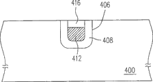
Afterwards, seeing also Fig. 4 D, serves as the cover curtain with patterning cover curtain layer 404 again, removes partly lining oxide layer 408 and partial oxidation layer 416, can reduce the height of (forming) of isolation structure in the irrigation canals and ditches 406, help the carrying out of follow-up manufacture of semiconductor by oxide layer 408 and oxide layer 416.Continue it, remove patterning cover curtain layer 404 and pad oxide 402.
In the manufacture method of above-mentioned semiconductor interconnect, in isolation structure, form semiconductor interconnect, can effectively dwindle the size of semiconductor element.On the other hand, the present invention integrates the processing procedure of intraconnections semiconductor interconnect (conductor layer 412) and the processing procedure of isolation structure, so can simplify semi-conductive manufacturing process in the time of reduction semiconductor element size.
The 3rd embodiment
Seeing also shown in Fig. 5 A, be the vertical view according to a kind of NOR type fast flash memory bank of the third embodiment of the present invention, the generalized section of B-B ' line that Fig. 5 B is Fig. 5 A, and Fig. 5 C is the generalized section of the C-C ' line of Fig. 5 A.
Please consult Fig. 5 A to Fig. 5 C simultaneously, the NOR type fast flash memory bank that present embodiment provided comprises a substrate 500, several control grids 502, several irrigation canals and ditches 504, several source areas 506, several drain areas 508, several isolation structures 510, several conducting blocks 514, several gates 516 of floating, several tunnel oxides 518 and dielectric layer 520.
Wherein, control grid 502 is arranged in the substrate 500 with directions X, and irrigation canals and ditches 504 are arranged in substrate 500 surfaces with the Y direction.Moreover source area 506 is positioned at the substrate 500 and irrigation canals and ditches 504 of control grid 502 1 sides, and drain area 508 lays respectively in the substrate 500 of 504 in irrigation canals and ditches of control grid 502 opposite sides.
Comprise one deck conductor layer 512 in each isolation structure 510, its material for example is a doped polycrystalline silicon.Wherein be arranged in the isolation structure 510 of the irrigation canals and ditches 504 of source area 506, its upper surface is lower than the upper surface of substrate 500, and expose conductor layer 512, in addition, each isolation structure 510 that is arranged in source area 508 irrigation canals and ditches 504 in addition fills up each irrigation canals and ditches 504, and conductor layer 512 is coated by isolation structure 510.
Conducting block 514 lays respectively in the irrigation canals and ditches 504 in the source area 506, and fills up irrigation canals and ditches 504, and electrically connects with source area 506 and conductor layer 512, and the material of conducting block 514 is the formula doped polycrystalline silicon for example.
Float gate 516 between the substrate 500 and control grid 502 between source area 506 and the drain area 508.
Tunnel oxide 518 is being floated between gate 516 and the substrate 500, and dielectric layer 520 is being floated between gate 516 and the control grid 502, and tunneling oxide layer 518 for example is a silica with the material of dielectric layer 520.
In addition, the NOR type fast flash memory bank of present embodiment more can comprise the several wires (not shown), can electrically connect each drain area 508 by contact hole 522 respectively.
In above-mentioned memory body,,, can effectively dwindle the memory body area so do not need with contact hole source electrode to be communicated with in addition again because in isolation structure 510, form semiconductor interconnect (conductor layer 512).
The 4th embodiment
Seeing also shown in Fig. 6 A~Fig. 6 G, is the manufacturing process profile according to the NOR type fast flash memory bank of the fourth embodiment of the present invention, and Fig. 6 A~Fig. 6 G is that hatching B-B ' in Fig. 5 A and C-C ' draw and form.
Please consult Fig. 6 A earlier, in a substrate 600, be provided with several source areas of arranging with X (please refer to Fig. 5 A 506) and drain area (please refer to Fig. 5 A 508), form several irrigation canals and ditches 602 of arranging with Y in substrate 600 surfaces again.And the mode that forms irrigation canals and ditches 606 can be with reference to existing technology, and the pad oxide 602 that for example forms patterning earlier in substrate 600 and patterning cover curtain layer 604 are with as etch mask, and the etching substrate 600 again, so that form several irrigation canals and ditches 606.Wherein, the material of pad oxide 602 for example is a silica, and the material of patterning cover curtain layer 604 for example is a silicon nitride.
Then, see also Fig. 6 B, in these irrigation canals and ditches 602, form several isolation structures 608, and be separated out several active regions 610.Wherein, isolation structure 608 is made up of dielectric layer 612 and conductor layer 614, and conductor layer 614 is coated by dielectric layer 612.The manufacture method of above-mentioned isolation structure 608, roughly the same with the manufacture method of the semiconductor interconnect of being introduced among second embodiment, so repeat no more in this.
Then, see also Fig. 6 C, earlier aforementioned pad oxide 602 and patterning cover curtain layer 604 are removed.Then, form tunnel oxide 616 in regular turn in source area in active region 610 and the substrate between drain area 600 again and the gate 618 of floating, its formation method for example is to form in regular turn to wear in substrate 600 to satisfy the oxidation material layer (not shown) and the gate material layer (not shown) of floating, and oxidation material layer and the gate material layer of floating carry out a patterning process and form it to wearing then.
Next, see also Fig. 6 D, in substrate 600, form a dielectric layer 620 that covers the gate 618 of floating.Then, between source area and drain area, form several control grids 622.The formation method of above-mentioned dielectric layer 620 and control grid 622, for example be in substrate 600, to form dielectric materials layer (not shown) and control grid material layer (not shown) in regular turn, dielectric materials layer and control grid material layer are carried out a patterning process and form it.
Afterwards, see also Fig. 6 E, remove the isolation structure 608 of a part in the irrigation canals and ditches 606 of source area, to expose conductor layer 614.Removing the partly method of isolation structure 608, for example is prior to forming a patterning photoresist layer 624 in the substrate 600, to expose the isolation structure 608 in the source area.Serve as the cover curtain then, isolation structure 608 is carried out an anisotropic etching processing procedure, to expose conductor layer 614 with patterning photoresist layer 624.Then, remove patterning photoresist layer 624.
Continue it, see also and form several conducting blocks 626 in the irrigation canals and ditches 606 of Fig. 6 F in source area, fill up irrigation canals and ditches 606 respectively, and be electrically connected at conductor layer 614.Wherein, the material of conducting block 626 for example is a doped polycrystalline silicon, and the method for its formation for example is prior to forming a conductor material layer 628 in the substrate 600.Then, conductor material layer 628 is carried out a planarization processing procedure, form it as the cmp processing procedure.
Subsequently, see also Fig. 6 G, form several doped regions 630 in the substrate 600 that exposes in source area and these drain areas, wherein the formation method of doped region for example is to carry out an ion implantation manufacture process.Thus, the doped region 630 in the source area is electrical connected by these conducting blocks 626.In addition, form after the doped region 630, can in substrate 600, form the several wires (not shown) that electrically connects each drain area respectively.
In the manufacture method of above-mentioned NOR type fast flash memory bank, the conductor layer 614 that utilization is formed in the isolation structure 608 connects each source area, replace in the known techniques and must form contact hole in the common source polar region, therefore the method that connects with lead again can effectively reduce the area of memory body.On the other hand, conductor layer 614 is formed in the isolation structure 608, has integrated the processing procedure of isolation structure and semiconductor interconnect, can simplify processing procedure and reduce manufacturing cost.
In sum, the present invention has following advantage at least:
1. in semiconductor interconnect and manufacture method thereof proposed by the invention, in isolation structure, form semiconductor interconnect, can effectively dwindle the size of semiconductor element.
2. the present invention integrates the processing procedure of intraconnections semiconductor interconnect and the processing procedure of isolation structure, so can simplify semi-conductive manufacturing process in the time of reduction semiconductor element size.
3. the NOR type fast flash memory bank of novelty of the present invention and its manufacture method are because form semiconductor interconnect, so do not need with contact hole source electrode to be communicated with in addition again in isolation structure.
4. because the NOR type fast flash memory bank utilization of novelty of the present invention forms semiconductor interconnect in isolation structure, therefore the source electrode that need not form in the known techniques is picked up line, the area of memory body can be dwindled.
5. NOR type fast flash memory bank proposed by the invention can reach the advantage of simplifying processing procedure and reducing manufacturing cost by the improvement on the processing procedure.
Though the present invention discloses as above with preferred embodiment; right its is not in order to limit the present invention; anyly have the knack of this skill person; without departing from the spirit and scope of the present invention; when can doing a little change and retouching, so protection scope of the present invention is as the criterion when looking accompanying the claim person of defining.