CN100511372C - Data driver, light emitting display device and driving method thereof - Google Patents
Data driver, light emitting display device and driving method thereof Download PDFInfo
- Publication number
- CN100511372C CN100511372C CNB2006100581378A CN200610058137A CN100511372C CN 100511372 C CN100511372 C CN 100511372C CN B2006100581378 A CNB2006100581378 A CN B2006100581378A CN 200610058137 A CN200610058137 A CN 200610058137A CN 100511372 C CN100511372 C CN 100511372C
- Authority
- CN
- China
- Prior art keywords
- data
- signal
- level phase
- converter
- passage
- Prior art date
- Legal status (The legal status is an assumption and is not a legal conclusion. Google has not performed a legal analysis and makes no representation as to the accuracy of the status listed.)
- Expired - Lifetime
Links
Images




Classifications
-
- G—PHYSICS
- G09—EDUCATION; CRYPTOGRAPHY; DISPLAY; ADVERTISING; SEALS
- G09G—ARRANGEMENTS OR CIRCUITS FOR CONTROL OF INDICATING DEVICES USING STATIC MEANS TO PRESENT VARIABLE INFORMATION
- G09G3/00—Control arrangements or circuits, of interest only in connection with visual indicators other than cathode-ray tubes
- G09G3/20—Control arrangements or circuits, of interest only in connection with visual indicators other than cathode-ray tubes for presentation of an assembly of a number of characters, e.g. a page, by composing the assembly by combination of individual elements arranged in a matrix no fixed position being assigned to or needed to be assigned to the individual characters or partial characters
- G09G3/22—Control arrangements or circuits, of interest only in connection with visual indicators other than cathode-ray tubes for presentation of an assembly of a number of characters, e.g. a page, by composing the assembly by combination of individual elements arranged in a matrix no fixed position being assigned to or needed to be assigned to the individual characters or partial characters using controlled light sources
- G09G3/30—Control arrangements or circuits, of interest only in connection with visual indicators other than cathode-ray tubes for presentation of an assembly of a number of characters, e.g. a page, by composing the assembly by combination of individual elements arranged in a matrix no fixed position being assigned to or needed to be assigned to the individual characters or partial characters using controlled light sources using electroluminescent panels
-
- G—PHYSICS
- G09—EDUCATION; CRYPTOGRAPHY; DISPLAY; ADVERTISING; SEALS
- G09G—ARRANGEMENTS OR CIRCUITS FOR CONTROL OF INDICATING DEVICES USING STATIC MEANS TO PRESENT VARIABLE INFORMATION
- G09G3/00—Control arrangements or circuits, of interest only in connection with visual indicators other than cathode-ray tubes
- G09G3/20—Control arrangements or circuits, of interest only in connection with visual indicators other than cathode-ray tubes for presentation of an assembly of a number of characters, e.g. a page, by composing the assembly by combination of individual elements arranged in a matrix no fixed position being assigned to or needed to be assigned to the individual characters or partial characters
- G09G3/22—Control arrangements or circuits, of interest only in connection with visual indicators other than cathode-ray tubes for presentation of an assembly of a number of characters, e.g. a page, by composing the assembly by combination of individual elements arranged in a matrix no fixed position being assigned to or needed to be assigned to the individual characters or partial characters using controlled light sources
- G09G3/30—Control arrangements or circuits, of interest only in connection with visual indicators other than cathode-ray tubes for presentation of an assembly of a number of characters, e.g. a page, by composing the assembly by combination of individual elements arranged in a matrix no fixed position being assigned to or needed to be assigned to the individual characters or partial characters using controlled light sources using electroluminescent panels
- G09G3/32—Control arrangements or circuits, of interest only in connection with visual indicators other than cathode-ray tubes for presentation of an assembly of a number of characters, e.g. a page, by composing the assembly by combination of individual elements arranged in a matrix no fixed position being assigned to or needed to be assigned to the individual characters or partial characters using controlled light sources using electroluminescent panels semiconductive, e.g. using light-emitting diodes [LED]
-
- G—PHYSICS
- G09—EDUCATION; CRYPTOGRAPHY; DISPLAY; ADVERTISING; SEALS
- G09G—ARRANGEMENTS OR CIRCUITS FOR CONTROL OF INDICATING DEVICES USING STATIC MEANS TO PRESENT VARIABLE INFORMATION
- G09G3/00—Control arrangements or circuits, of interest only in connection with visual indicators other than cathode-ray tubes
- G09G3/20—Control arrangements or circuits, of interest only in connection with visual indicators other than cathode-ray tubes for presentation of an assembly of a number of characters, e.g. a page, by composing the assembly by combination of individual elements arranged in a matrix no fixed position being assigned to or needed to be assigned to the individual characters or partial characters
-
- G—PHYSICS
- G09—EDUCATION; CRYPTOGRAPHY; DISPLAY; ADVERTISING; SEALS
- G09G—ARRANGEMENTS OR CIRCUITS FOR CONTROL OF INDICATING DEVICES USING STATIC MEANS TO PRESENT VARIABLE INFORMATION
- G09G2300/00—Aspects of the constitution of display devices
- G09G2300/08—Active matrix structure, i.e. with use of active elements, inclusive of non-linear two terminal elements, in the pixels together with light emitting or modulating elements
-
- G—PHYSICS
- G09—EDUCATION; CRYPTOGRAPHY; DISPLAY; ADVERTISING; SEALS
- G09G—ARRANGEMENTS OR CIRCUITS FOR CONTROL OF INDICATING DEVICES USING STATIC MEANS TO PRESENT VARIABLE INFORMATION
- G09G2310/00—Command of the display device
- G09G2310/02—Addressing, scanning or driving the display screen or processing steps related thereto
- G09G2310/0264—Details of driving circuits
- G09G2310/027—Details of drivers for data electrodes, the drivers handling digital grey scale data, e.g. use of D/A converters
-
- G—PHYSICS
- G09—EDUCATION; CRYPTOGRAPHY; DISPLAY; ADVERTISING; SEALS
- G09G—ARRANGEMENTS OR CIRCUITS FOR CONTROL OF INDICATING DEVICES USING STATIC MEANS TO PRESENT VARIABLE INFORMATION
- G09G2310/00—Command of the display device
- G09G2310/02—Addressing, scanning or driving the display screen or processing steps related thereto
- G09G2310/0264—Details of driving circuits
- G09G2310/0297—Special arrangements with multiplexing or demultiplexing of display data in the drivers for data electrodes, in a pre-processing circuitry delivering display data to said drivers or in the matrix panel, e.g. multiplexing plural data signals to one D/A converter or demultiplexing the D/A converter output to multiple columns
-
- G—PHYSICS
- G09—EDUCATION; CRYPTOGRAPHY; DISPLAY; ADVERTISING; SEALS
- G09G—ARRANGEMENTS OR CIRCUITS FOR CONTROL OF INDICATING DEVICES USING STATIC MEANS TO PRESENT VARIABLE INFORMATION
- G09G2320/00—Control of display operating conditions
- G09G2320/02—Improving the quality of display appearance
- G09G2320/0233—Improving the luminance or brightness uniformity across the screen
Landscapes
- Engineering & Computer Science (AREA)
- Physics & Mathematics (AREA)
- Computer Hardware Design (AREA)
- General Physics & Mathematics (AREA)
- Theoretical Computer Science (AREA)
- Control Of Indicators Other Than Cathode Ray Tubes (AREA)
- Control Of El Displays (AREA)
Abstract
本发明提供了一种适于显示亮度基本均匀的图像的数据驱动器。该数据驱动器包括:保持锁存器单元,包括用来存储数据的保持锁存器;信号发生器,包括用来接收数据以产生数据信号的数-模转换器;第一开关单元,设置在保持锁存器单元和信号发生器之间;第二开关单元,与信号发生器结合,用来将数据信号发送给数据线。第一开关单元在水平期期间,以与前一水平期期间使保持锁存器与数-模转换器相互结合的方式不同的方式,使保持锁存器与数-模转换器结合。因此,扩散了数-模转换器的误差,从而能够显示亮度基本均匀的图像。

The present invention provides a data driver suitable for displaying images with substantially uniform brightness. The data driver includes: a holding latch unit, including a holding latch for storing data; a signal generator, including a digital-to-analog converter for receiving data to generate a data signal; a first switch unit, configured to hold Between the latch unit and the signal generator; the second switch unit, combined with the signal generator, is used to send the data signal to the data line. The first switching unit couples the holding latch with the digital-analog converter during the horizontal period in a manner different from that of the holding latch and the digital-analog converter during the previous horizontal period. Therefore, the error of the digital-to-analog converter is diffused, so that an image with substantially uniform brightness can be displayed.
Description
技术领域 technical field
本发明涉及一种数据驱动器、一种采用该数据驱动器的发光显示装置和一种驱动该发光显示装置的方法,更具体地讲,涉及一种适于显示亮度基本均匀的图像的数据驱动器、一种采用该数据驱动器的发光显示装置和一种驱动该发光显示装置的方法。The present invention relates to a data driver, a light-emitting display device using the data driver and a method for driving the light-emitting display device, more particularly, to a data driver suitable for displaying images with substantially uniform brightness, a A light-emitting display device using the data driver and a method for driving the light-emitting display device.
背景技术 Background technique
近来,已经开发了比阴极射线管(CRT)重量轻、体积小的各种平板显示装置(FPD)。FPD包括液晶显示装置(LCD)、场发射显示装置(FED)、等离子体显示面板(PDP)和发光显示装置。Recently, various flat panel display devices (FPDs) that are lighter in weight and smaller in size than cathode ray tubes (CRTs) have been developed. The FPD includes a liquid crystal display device (LCD), a field emission display device (FED), a plasma display panel (PDP), and a light emitting display device.
在FPD中,发光显示装置采用电致发光(EL)装置来显示图像,其中,电致发光装置通过电子和空穴的复合来产生光。发光显示装置具有高的响应速度且以低功耗驱动。Among the FPDs, light emitting display devices display images using electroluminescence (EL) devices that generate light through recombination of electrons and holes. The light emitting display device has a high response speed and is driven with low power consumption.
发光显示装置包括位于数据线和扫描线的方向之间的交叉区域内的像素。当将扫描信号提供给扫描线时选择像素,以对像素充以与提供给数据线的数据信号对应的电压。像素提供与对EL装置的充电电压对应的电流来产生预定亮度的光。由每个像素发射的预定亮度的光形成光的分量,并使这些分量结合而在显示区内显示预定的图像。A light emitting display device includes pixels located in intersection regions between directions of data lines and scan lines. A pixel is selected when a scan signal is supplied to the scan line to charge the pixel with a voltage corresponding to a data signal supplied to the data line. The pixels supply current corresponding to the charging voltage to the EL device to generate light of a predetermined brightness. Light of predetermined luminance emitted by each pixel forms light components, and these components are combined to display a predetermined image in the display area.
因此,发光显示装置包括将数据信号提供给数据线的数据驱动部分和将扫描信号提供给扫描线的扫描驱动器。数据驱动部分包括至少一个具有预定通道(channel)的数据驱动器。Accordingly, the light emitting display device includes a data driving part that supplies data signals to the data lines and a scan driver that supplies scan signals to the scan lines. The data driving part includes at least one data driver having a predetermined channel.
图1示出了传统的数据驱动器60。为了方便起见,在图1中,假设传统的数据驱动器60包括j(j为自然数)个通道。FIG. 1 shows a conventional data driver 60 . For convenience, in FIG. 1 , it is assumed that the conventional data driver 60 includes j (j is a natural number) channels.
参照图1,传统的数据驱动器包括移位寄存器单元1、采样锁存器单元2、保持锁存器单元3、信号发生器4和输出级5。Referring to FIG. 1 , a conventional data driver includes a
移位寄存器单元1接收来自外面的源起始脉冲SSP和源移位时钟SSC。在源移位时钟SSC的每个周期,移位寄存器单元1在将源起始脉冲SSP移位的同时顺序地产生j个采样信号。因此,移位寄存器单元1包括j个移位寄存器11至1j。The
采样锁存器单元2响应由移位寄存器单元1顺序提供的采样信号来顺序地存储数据Data。因此,采样锁存器单元2包括用来存储j个数据Data的j个采样锁存器21至2j。The
保持锁存器单元3从采样锁存器单元2接收数据Data来存储数据Data。保持锁存器单元3将存储在其内的数据Data提供给信号发生器4。因此,保持锁存器单元3包括j个保持锁存器31至3j。The holding latch unit 3 receives the data Data from the
信号发生器4接收由保持锁存器单元3提供的数据Data来产生j个数据信号以与接收的数据Data对应。因此,信号发生器4包括j个数-模转换器(DAC)41至4j。即,信号发生器4采用设置在通道中的DAC 41至4j产生j个数据信号,以将产生的数据信号提供给输出级5。The signal generator 4 receives the data Data provided by the holding latch unit 3 to generate j data signals corresponding to the received data Data. Therefore, the signal generator 4 includes j digital-to-analog converters (DACs) 41 to 4j. That is, the signal generator 4 generates j data signals using the DACs 41 to 4j provided in the channels to supply the generated data signals to the output stage 5.
输出级5将由信号发生器4提供的j个数据信号提供给j条数据线D1至Dj。然后,将数据信号提供给像素,从而显示预定的图像。The output stage 5 supplies j data signals provided by the signal generator 4 to the j data lines D1 to Dj. Then, the data signal is supplied to the pixels, thereby displaying a predetermined image.
然而,根据传统的数据驱动器,通常,由于设置在通道中的DAC 41至4j的偏差而导致不可能产生均匀的数据信号。实际上,即使在制造DAC 41至4j时精确地控制制造过程,DAC 41至4j通常也具有大约±3mV的偏差。因此,虽然向DAC 41至4j输入具有相同灰阶值的数据Data,但是产生了具有不同电压值(或电流值)的数据信号。如上所述,如果向DAC 41至4j输入相同灰阶值时产生具有不同电压值(或电流值)的数据信号,则在发光显示装置上显示亮度不均匀的图像。具体地讲,当具有高偏差的DAC 41至4j彼此相邻时,额外地产生了处于垂直线的形式的噪声。However, according to the conventional data driver, generally, it is impossible to generate a uniform data signal due to deviation of the DACs 41 to 4j provided in the channels. Actually, even if the manufacturing process is precisely controlled when manufacturing the DACs 41 to 4j, the DACs 41 to 4j usually have a deviation of about ±3mV. Therefore, although data Data having the same grayscale value is input to the DACs 41 to 4j, data signals having different voltage values (or current values) are generated. As described above, if data signals having different voltage values (or current values) are generated when the same gray scale value is input to the DACs 41 to 4j, an image with uneven brightness is displayed on the light emitting display device. Specifically, when the DACs 41 to 4j having high deviations are adjacent to each other, noise in the form of vertical lines is additionally generated.
因此,需要减小由发光显示装置的数据驱动器中使用的数-模转换器的制造和加工方面的不均匀性而造成的图像亮度的不均匀性。Accordingly, there is a need to reduce unevenness in image brightness caused by unevenness in manufacturing and processing of a digital-to-analog converter used in a data driver of a light-emitting display device.
发明内容 Contents of the invention
因此,本发明提供了一种适于显示亮度基本均匀的图像的数据驱动器、一种采用该数据驱动器的发光显示装置和一种驱动该发光显示装置的方法。数据驱动器在帧期间驱动发光显示装置,其中,帧被划分为水平期。一帧可包括一个或多个水平期。Accordingly, the present invention provides a data driver suitable for displaying images with substantially uniform luminance, a light emitting display device using the data driver, and a method of driving the light emitting display device. The data driver drives the light emitting display device during a frame, which is divided into horizontal periods. A frame may include one or more horizontal periods.
根据本发明的一方面,提供了一种数据驱动器,其包括:保持锁存器单元,包括用来存储数据的保持锁存器;信号发生器,包括用来接收数据以产生数据信号的数-模转换器;第一开关单元,设置在保持锁存器单元和信号发生器之间;第二开关单元,与信号发生器结合,用来将数据信号发送给数据线。第一开关单元在当前水平期期间,以与前一水平期期间使保持锁存器与数-模转换器相互结合的方式不同的方式,使保持锁存器与数-模转换器结合。According to an aspect of the present invention, a data driver is provided, which includes: a holding latch unit, including a holding latch for storing data; a signal generator, including a data- The analog-to-analog converter; the first switch unit is arranged between the holding latch unit and the signal generator; the second switch unit is combined with the signal generator to send the data signal to the data line. The first switching unit combines the holding latch with the digital-analog converter during the current horizontal period differently from the way the holding latch and the digital-analog converter are combined with each other during the previous horizontal period.
信号发生器例如可包括其数目比保持锁存器的数目多至少一个的数-模转换器。第一开关单元在前一水平期期间将数据向左或右移位,而在当前水平期期间不将数据移位。The signal generator may, for example, include at least one more digital-to-analog converter than the number of holding latches. The first switching unit shifts data to the left or right during a previous horizontal period and does not shift data during a current horizontal period.
根据本发明的另一方面,提供了一种发光显示装置,其包括:扫描驱动器,用来驱动扫描线;数据驱动部分,用来驱动数据线;显示区,包括与扫描线和数据线结合的像素。数据驱动部分包括:保持锁存器单元,包括用来存储数据的保持锁存器;信号发生器,包括用来接收数据以产生数据信号的数-模转换器;第一开关单元,设置在保持锁存器单元和信号发生器之间;第二开关单元,与信号发生器结合,用来将数据信号发送给数据线。第一开关单元在当前水平期期间,以与前一水平期期间使保持锁存器与数-模转换器相互结合的方式不同的方式,使保持锁存器与数-模转换器结合。According to another aspect of the present invention, a light-emitting display device is provided, which includes: a scan driver, used to drive scan lines; a data drive part, used to drive data lines; a display area, including pixels. The data driving part includes: a holding latch unit, including a holding latch for storing data; a signal generator, including a digital-to-analog converter for receiving data to generate a data signal; Between the latch unit and the signal generator; the second switch unit, combined with the signal generator, is used to send the data signal to the data line. The first switching unit combines the holding latch with the digital-analog converter during the current horizontal period differently from the way the holding latch and the digital-analog converter are combined with each other during the previous horizontal period.
根据本发明的另一方面,提供了一种驱动发光显示装置的方法,该方法包括利用数-模转换器产生数据信号、通过数据线将数据信号提供给像素和通过像素产生与数据信号对应的预定的光分量。用来在当前水平期期间将数据信号提供给特定数据线的数-模转换器不同于用来在前一水平期期间将数据信号提供给该特定数据线的数-模转换器。According to another aspect of the present invention, there is provided a method for driving a light-emitting display device, the method comprising generating a data signal by a digital-to-analog converter, supplying the data signal to a pixel through a data line, and generating a signal corresponding to the data signal through the pixel. Predetermined light component. The digital-to-analog converter used to supply a data signal to a particular data line during a current horizontal period is different from the digital-to-analog converter used to supply a data signal to that particular data line during a previous horizontal period.
数据信号的产生例如可包括:在保持锁存器中存储数据;在两个相邻的水平期中的至少一个水平期期间,将存储在保持锁存器中的数据移位,以将数据提供给数-模转换器;利用数据产生数据信号;在这两个水平期中的至少一个水平期内,将数据信号移位,以将数据信号提供给数据线。The generation of the data signal may include, for example: storing data in a holding latch; during at least one horizontal period of two adjacent horizontal periods, shifting the data stored in the holding latch to provide the data to A digital-to-analog converter; generating a data signal from the data; shifting the data signal during at least one of the two horizontal periods to supply the data signal to the data line.
附图说明 Description of drawings
通过结合附图对示例性实施例进行下列描述,本发明的这些和/或其他方面和特点将会变得更加清楚且更加易于理解,附图中:These and/or other aspects and features of the present invention will become clearer and easier to understand by carrying out the following description of exemplary embodiments in conjunction with the accompanying drawings, in which:
图1示出了传统的数据驱动器;Figure 1 shows a conventional data driver;
图2示出了根据本发明实施例的发光显示装置;Fig. 2 shows a light-emitting display device according to an embodiment of the present invention;
图3示出了图2中示出的数据驱动器的一个例子;Figure 3 shows an example of the data driver shown in Figure 2;
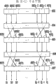
图4A至图4C示出了图3中示出的第一开关单元和第二开关单元的操作过程的一个例子;4A to 4C show an example of the operation process of the first switch unit and the second switch unit shown in FIG. 3;
图5A至图5C示出了图3中示出的第一开关单元和第二开关单元的操作过程的另一个例子;5A to 5C show another example of the operation process of the first switch unit and the second switch unit shown in FIG. 3;
图6示出了图2中示出的数据驱动器的另一个例子;Fig. 6 shows another example of the data driver shown in Fig. 2;
图7示出了图2中示出的数据驱动器的又一个例子。FIG. 7 shows still another example of the data driver shown in FIG. 2 .
具体实施方式 Detailed ways
以下,将参照所附图2至图7来描述本发明的示例性实施例。Hereinafter, exemplary embodiments of the present invention will be described with reference to the accompanying FIGS. 2 to 7 .
图2示出了根据本发明实施例的发光显示装置。FIG. 2 shows a light emitting display device according to an embodiment of the present invention.
参照图2,根据本发明实施例的发光显示装置包括:显示区300,包括与扫描线S1至Sn和数据线D1至Dm结合的像素400;扫描驱动器100,用来驱动扫描线S1至Sn;数据驱动部分200,用来驱动数据线D1至Dm;时序控制器500,用来控制扫描驱动器100和数据驱动部分200。Referring to FIG. 2, the light-emitting display device according to an embodiment of the present invention includes: a
时序控制器500响应由外面提供的同步信号来产生数据驱动控制信号DCS和扫描驱动控制信号SCS。由时序控制器500产生的数据驱动控制信号DCS被提供给数据驱动部分200,由时序控制器500产生的扫描驱动控制信号SCS被提供给扫描驱动器100。时序控制器500还将由外面提供的数据Data提供给数据驱动部分200。The
扫描驱动器100从时序控制器500接收扫描驱动控制信号SCS。扫描驱动器100将扫描信号顺序地提供给扫描线S1至Sn。即,扫描驱动器100在将扫描信号顺序地提供给扫描线S1至Sn的同时,选择被提供给数据信号的像素400。The
数据驱动部分200从时序控制器500接收数据驱动控制信号DCS和数据Data。然后,数据驱动部分200产生预定的电流或电压作为数据信号以与数据Data的灰阶值对应。这里,当预定的电压被作为数据信号产生时,数据驱动部分200将数据信号提供给通过扫描信号选择的像素400。当预定的电流被作为数据信号产生时,数据驱动部分200从通过扫描信号选择的像素400接收预定的电流(即,数据驱动部分200作为电流接收器(current sink)来工作)。因此,数据驱动部分200包括至少一个数据驱动器600。数据驱动器600在帧期间驱动像素400。每个帧周期可被划分为一个或多个水平期。随后会详细描述数据驱动器600的结构。The
显示区300包括在扫描线S1至Sn和数据线D1至Dm的方向之间的交叉区域形成的像素400。像素400从第一电源ELVDD接收第一功率,从第二电源ELVSS接收第二功率。在一些实施例中,第二电源可以为地电压,或者可以根本不包括第二电源。像素400被充至与数据信号对应的预定电压,并且通过电致发光装置(未示出)将与来自第一电源ELVDD的充电电压对应的电流提供给第二电源ELVSS,从而显示了预定亮度的图像。The
图3示出了根据本发明第一实施例的数据驱动器。在图3中,为了方便起见,假设数据驱动器600包括j个通道。Fig. 3 shows a data driver according to a first embodiment of the present invention. In FIG. 3 , it is assumed that the
参照图3,根据本发明第一实施例的数据驱动器600包括移位寄存器单元601、采样锁存器单元602、保持锁存器单元603、第一开关单元604、信号发生器605、第二开关单元606和输出级607。Referring to FIG. 3, the
移位寄存器单元601接收来自外面的源起始脉冲SSP和源移位时钟SSC。然后,在源移位时钟SSC的每个周期,移位寄存器单元601在将源起始脉冲SSP移位的同时顺序地产生j个采样信号。因此,移位寄存器单元601包括j个移位寄存器6011至601j。The
采样锁存器单元602响应由移位寄存器单元601顺序提供的采样信号来顺序地存储数据Data。因此,采样锁存器单元602包括用来存储j个数据Data的j个采样锁存器6021至602j。这里,采样锁存器6021至602j的存储容量的设定方式是,采样锁存器6021至602j可存储预定位的数据Data。The
保持锁存器单元603从采样锁存器单元602接收数据Data来存储数据Data。保持锁存器单元603将存储在其内的数据Data提供给第一开关单元604。因此,保持锁存器单元603包括j个保持锁存器6031至603j。这里,保持锁存器6031至603j的存储容量的设定方式是,保持锁存器6031至603j可存储预定位的数据Data。The holding
第一开关单元604从保持锁存器单元603接收数据Data。然后,第一开关单元604将数据Data发送到信号发生器605。此时,在每个水平期,第一开关单元604使保持锁存器6031至603j与不同的DAC 6051至605h结合。例如,在第k(k为自然数)个水平期期间,第一开关单元604可使第一保持锁存器6031与第一DAC 6051结合;在第(k+1)个水平期期间,第一开关单元604可使第一保持锁存器6031与第二DAC 6052结合。The
这样,信号发生器605从第一开关单元604接收数据Data,并产生数据信号以与接收的数据Data对应。因此,信号发生器605包括h(h为不小于j的自然数)个DAC 6051至605h。这里,在信号发生器605中包括的DAC 6051至605h的数目不小于j。下面将对其进行详细的描述。In this way, the
在信号发生器605中包括的DAC 6051至605h产生预定的电流或电压以与数据Data的灰阶值对应。然后,信号发生器605将产生的数据信号提供给第二开关单元606。当通过信号发生器605产生电压数据信号时,输出级607包括缓冲器6071至607j。另一方面,当通过信号发生器605产生电流数据信号时,输出级607包括采样/保持电路6071至607j。The
第二开关单元606从信号发生器605接收数据信号。然后,在每个水平期,第二开关单元606使DAC 6051至605h与不同的缓冲器6071至607j结合,或者使DAC 6051至605h与不同的采样/保持电路6071至607j结合。例如,在第k个水平期期间,第二开关单元606可使第一缓冲器6071(或第一采样/保持电路6071)与第一DAC 6051结合;在第(k+1)个水平期期间,第二开关单元606可使第一缓冲器6071(或第一采样/保持电路6071)与第二DAC6052结合。实际上,第二开关单元606控制信号发生器605和输出级607之间的连接,使得由存储在第i(i为自然数)个保持锁存器603i内的数据Data产生的数据信号可被提供给第i个缓冲器607i(或第i个采样/保持电路607i)。The
输出级607从第二开关单元606接收j个数据信号。当由第二开关单元606提供电流数据信号时,设置在输出级607中的采样/保持电路6071至607j通过数据线对像素充以与提供给像素的电流数据信号对应的电压。然后,采样/保持电路6071至607j通过数据线D1至Dj从像素400接收预定的电流,所述预定的电流与充入像素中的电压对应。换言之,采样/保持电路6071至607j作为电流接收器来工作。另一方面,如果由第二开关单元606提供电压数据信号时,那么通过缓冲器6071至607j将这些电压数据信号提供给数据线D1至Dj。The
图4A至图4C示出了第一开关单元604和第二开关单元606的操作的例子。这里,假设在信号发生器605中包括其数目比通道的数目多二的DAC6050至605j+1。例如,如果数据驱动器600与100条数据线D1至D100结合,那么在信号发生器605中包括102个DAC。4A to 4C illustrate examples of operations of the
参照图4A至图4C,在第k个水平期期间,第一开关单元604将存储在保持锁存器6031至603j中的数据Data向左移位一个通道,以将数据Data提供给DAC 6050至605j-1。然后,DAC 6050至605j-1产生电流数据信号或电压数据信号以与提供给它们的数据Data对应,以将电流数据信号或电压数据信号提供给第二开关单元606。此时,第二开关单元606将DAC 6050至605j-1提供的电流数据信号或电压数据信号向右移位一个通道,以将电流数据信号或电压数据信号提供给输出级607。即,第二开关单元606控制信号发生器605和输出级607之间的连接,使得由第i个保持锁存器提供的数据产生的数据信号可被提供给第i条数据线。Referring to FIGS. 4A to 4C, during the kth horizontal period, the
如图4B中所示,在第(1k+1)个水平期期间,第一开关单元604将存储在保持锁存器6031至603j中的数据Data提供给设置在初始通道中的DAC 6051至605j。然后,DAC 6051至605j产生电流数据信号或电压数据信号以与提供给它们的数据Data对应,以将电流数据信号或电压数据信号提供给第二开关单元606。此时,第二开关单元将由DAC 6051至605jj输出的数据信号提供给输出级607而没有将数据信号移位。As shown in FIG. 4B, during the (1k+1)th horizontal period, the
如图4C中所示,在第(k+2)个水平期期间,第一开关单元604将存储在保持锁存器6031至603j中的数据Data向右移位一个通道,以将数据Data提供给DAC 6052至605j+1。然后,DAC 6052至605j+1产生电流数据信号或电压数据信号以与提供给它们的数据Data对应,以将电流数据信号或电压数据信号提供给第二开关单元606。此时,第二开关单元606将由DAC 6052至605j+1提供的电流数据信号或电压数据信号向左移位一个通道,以将电流数据信号或电压数据信号提供给输出级607。As shown in FIG. 4C, during the (k+2)th horizontal period, the
如上所述,在根据本发明的数据驱动器中,在第k个水平期期间与特定的保持锁存器结合的DAC不同于在第(k+1)个水平期期间与特定的保持锁存器结合的DAC。因此,在各水平期期间提供给数据线D1至Dj的数据信号通过与在前一水平期期间产生数据信号的DAC不同的DAC来产生。如上所述,如果在各水平期期间产生提供给数据线D1至Dj的数据信号的DAC不同于产生前一水平期的数据信号的DAC,那么显示区300可显示亮度基本均匀的图像。As described above, in the data driver according to the present invention, the DAC combined with the specific holding latch during the k-th horizontal period is different from the DAC combined with the specific holding latch during the (k+1)-th horizontal period. Combined DAC. Therefore, the data signals supplied to the data lines D1 to Dj during each horizontal period are generated by a DAC different from the DAC that generated the data signals during the previous horizontal period. As described above, if the DAC generating the data signals supplied to the data lines D1 to Dj during each horizontal period is different from the DAC generating the data signals of the previous horizontal period, the
换言之,为了减小或防止由于DAC的制造过程而导致DAC中存在的不均匀性对图像亮度的影响,从一个水平期到下一水平期产生数据信号的DAC是不同的。即,当在每个水平期通过均具有自身偏差的DAC产生的数据信号被提供给不同的数据线D1至Dj时,使误差扩散,从而能够显示亮度基本均匀的图像。另一方面,根据本发明,开关单元604和606的连接过程不局限于图4A至图4C中示出的内容,而是可以变化使得在每个连续的水平期由与前一水平期的DAC不同的DAC产生的数据信号可被提供给数据线D1至Dj。In other words, in order to reduce or prevent the influence of non-uniformity existing in the DAC due to the manufacturing process of the DAC on image brightness, the DAC generating the data signal is different from one horizontal period to the next horizontal period. That is, when data signals generated by DACs each having its own deviation are supplied to different data lines D1 to Dj every horizontal period, errors are diffused so that an image with substantially uniform brightness can be displayed. On the other hand, according to the present invention, the connection process of the
图5A至图5C示出了第一开关单元604和第二开关单元606的操作过程的另一实施例。这里,假设在信号发生器605中包括其数目与通道的数目相同的DAC 6051至605j。5A to 5C illustrate another embodiment of the operation process of the
参照图5A至图5C,在第k个水平期期间,第一开关单元604将存储在一些保持锁存器例如6031和603j-2中的数据Data向右移位两个通道,并将存储在其余的保持锁存器例如6032,6033…603j-3,603j-1和603j中的数据向左移位一个通道,以将数据Data提供给DAC 6051至605j。然后,DAC 6051至605j产生与提供给它们的数据Data对应的电流数据信号或电压数据信号,以将电流数据信号或电压数据信号提供给第二开关单元606。然后,第二开关单元606在将数据信号提供给输出级607之前,将DAC 6051至605j提供的电流数据信号或电压数据信号中的一些数据信号向左移位两个通道,并将其余的数据信号向右移位一个通道。即,第二开关单元606控制信号发生器605和输出级607之间的连接,使得通过由第i个保持锁存器提供的数据产生的数据信号可被提供给第i条数据线。5A to 5C, during the kth horizontal period, the
如图5B中所示,在第(k+1)个水平期期间,第一开关单元604将存储在保持锁存器6031至603j中的数据Data提供给设置在初始通道中的DAC 6051至605j而没有将数据Data移位。然后,DAC 6051至605j产生电流数据信号或电压数据信号以与提供给它们的数据Data对应,并将电流数据信号或电压数据信号提供给第二开关单元606。此时,第二开关单元606将由DAC6051至605j提供的数据信号提供给输出级607而没有将数据信号移位。As shown in FIG. 5B, during the (k+1)th horizontal period, the
如图5C中所示,在第(k+2)个水平期期间,第一开关单元604将存储在一些保持锁存器例如6033和603j中的数据Data向左移位两个通道,并将存储在其余的保持锁存器例如6031,6032,6034…603j-1中的数据Data向右移位一个通道,以将数据Data提供给DAC 6051至605j。然后,DAC 6051至605j产生与提供给它们的数据Data对应的电流数据信号或电压数据信号,并将电流数据信号或电压数据信号提供给第二开关单元606。此时,第二开关单元606将DAC 6051至605j提供的电流数据信号或电压数据信号中的一些数据信号向右移位两个通道,并将其余的数据信号向左移位一个通道,以将数据信号提供给输出级607。As shown in FIG. 5C, during the (k+2)th horizontal period, the
如上所述,在根据本发明的数据驱动器600中,在第k个水平期期间保持锁存器单元603和信号发生器605之间的连接不同于在第(k+1)个水平期期间保持锁存器单元603和信号发生器605之间的连接。因此,在各水平期期间提供给数据线Di的数据信号通过与在前一水平期期间产生提供给同一数据线的信号的DAC不同的DAC来产生。如上所述,当在每个水平期由与前一水平期的DAC不同的DAC产生的数据信号被提供给数据线D1至Dj时,显示区300可显示亮度基本均匀的图像。As described above, in the
即,当在每个水平期通过具有偏差的DAC产生的数据信号被提供给不同的数据线D1至Dj时,使由于DAC的偏差而导致的误差扩散,从而能够显示亮度基本均匀的图像。另一方面,根据本发明,开关单元604和606之间的连接过程不局限于图5A至图5C中示出的内容,而是可以变化,使得在下一水平期期间通过与在前一个水平期期间产生数据信号的DAC不同的DAC产生的数据信号可被提供给数据线D1至Dj。That is, when a data signal generated by a DAC having a deviation is supplied to different data lines D1 to Dj in each horizontal period, an error due to the deviation of the DAC is diffused, thereby being able to display an image with substantially uniform brightness. On the other hand, according to the present invention, the connection process between the switching
图6示出了根据本发明第二实施例的数据驱动器600′。在图6中,用相同的标号表示也在图3中出现的元件,并省略对它们的详细描述。FIG. 6 shows a data driver 600' according to a second embodiment of the present invention. In FIG. 6, elements that also appear in FIG. 3 are denoted by the same reference numerals, and their detailed descriptions are omitted.
参照图6,在根据本发明第二实施例的数据驱动器600′中,信号发生器609产生电流数据信号以与由第一开关单元604提供的数据Data对应。因此,信号发生器609包括DAC 6091至609h。然后,DAC 6091至609h通过第二开关单元606和数据线D1至Dj从像素400接收电流。换言之,这些DAC作为电流接收器来工作。随后,像素400产生预定亮度的光分量以与提供给数据驱动器600′的电流对应。Referring to FIG. 6 , in a
除了在第二实施例600′的信号发生器609中包括的DAC 6091至609h通过第二开关单元606和数据线D1至Dj从像素400接收电流之外,本发明的第二实施例600′的结构与第一实施例600的结构相同。因此,在本发明的第二实施例600′中,省略了输出级607,因而第二开关单元606与数据线D1至Dj直接结合。另外,第一开关单元604第二开关单元606的操作与图4A至图4C或者图5A至图5C中示出的操作相同。Except that the
图7示出了根据本发明第三实施例的数据驱动器600″。在图7中,用相同的标号表示也在图3中示出的元件,并且省略对它们的详细描述。Fig. 7 shows a
参照图7,根据本发明第三实施例的数据驱动器600″还包括与保持锁存器单元603结合的电平转换器单元610。电平转换器单元610在将数据Data提供给第一开关单元604之前,升高由保持锁存器单元603提供的数据Data的电压电平。当具有高电压电平的数据Data由外面系统提供给数据驱动器600″时,在发光显示装置中必须设置耐高电压电平的电路部分,从而增加了制造费用。因此,由数据驱动器600″的外面提供具有低电压电平的数据Data,并且通过电平转换器单元610将具有低电压电平的数据Data转换成高电压电平。于是,与低电压电平对应的电路部分可用在发光显示装置中,从而能够降低制造费用。Referring to Fig. 7, the
如上所述,在根据本发明实施例的数据驱动器、采用该数据驱动器的发光显示装置及其驱动方法中,在一水平期期间保持锁存器单元和信号发生器之间的连接不同于在下一水平期期间保持锁存器单元和信号发生器之间的连接。因此,在各水平期期间提供给数据线的数据信号通过与在前一或下一周期期间提供的产生数据信号的DAC不同的DAC产生。这样,扩散了由DAC造成的误差,因而能够显示亮度基本均匀的图像。As described above, in the data driver, the light-emitting display device using the data driver and the driving method thereof according to the embodiment of the present invention, maintaining the connection between the latch unit and the signal generator during one horizontal period is different from maintaining the connection between the latch unit and the signal generator during the next horizontal period. The connection between the latch unit and the signal generator is maintained during the horizontal period. Therefore, the data signal supplied to the data line during each horizontal period is generated by a DAC different from the DAC generating the data signal supplied during the previous or next period. In this way, the error caused by the DAC is diffused, so that an image with substantially uniform brightness can be displayed.
虽然已经示出和描述了本发明的示例性实施例,但是本领域的技术人员应该理解,在不脱离本发明的原则和精神的情况下,可对实施例进行变化,其中,该发明的范围限定在权利要求及其等同物中。While exemplary embodiments of the present invention have been shown and described, it will be appreciated by those skilled in the art that changes may be made to the embodiments without departing from the principles and spirit of the invention, wherein the scope of the invention defined in the claims and their equivalents.
本申请要求于2005年4月28日提交到韩国知识产权局的第10-2005-0035755号韩国专利申请的优先权和权益,该申请的全部内容通过引用公开于此。This application claims priority and benefit from Korean Patent Application No. 10-2005-0035755 filed with the Korean Intellectual Property Office on April 28, 2005, the entire contents of which are hereby incorporated by reference.
Claims (20)
Applications Claiming Priority (2)
| Application Number | Priority Date | Filing Date | Title |
|---|---|---|---|
| KR1020050035755A KR100707634B1 (en) | 2005-04-28 | 2005-04-28 | Data driving circuit, light emitting display device and driving method thereof |
| KR1020050035755 | 2005-04-28 |
Publications (2)
| Publication Number | Publication Date |
|---|---|
| CN1855199A CN1855199A (en) | 2006-11-01 |
| CN100511372C true CN100511372C (en) | 2009-07-08 |
Family
ID=37195328
Family Applications (1)
| Application Number | Title | Priority Date | Filing Date |
|---|---|---|---|
| CNB2006100581378A Expired - Lifetime CN100511372C (en) | 2005-04-28 | 2006-03-06 | Data driver, light emitting display device and driving method thereof |
Country Status (4)
| Country | Link |
|---|---|
| US (1) | US7982691B2 (en) |
| JP (1) | JP2006309142A (en) |
| KR (1) | KR100707634B1 (en) |
| CN (1) | CN100511372C (en) |
Families Citing this family (3)
| Publication number | Priority date | Publication date | Assignee | Title |
|---|---|---|---|---|
| TWI522982B (en) * | 2010-12-31 | 2016-02-21 | 友達光電股份有限公司 | Source driver |
| KR101919502B1 (en) * | 2012-04-27 | 2018-11-19 | 삼성디스플레이 주식회사 | Data Driver and Driving Method of Light Emitting Display Device Using the same |
| KR102225324B1 (en) * | 2014-06-09 | 2021-03-10 | 삼성디스플레이 주식회사 | Data driver |
Family Cites Families (35)
| Publication number | Priority date | Publication date | Assignee | Title |
|---|---|---|---|---|
| US5162670A (en) | 1990-01-26 | 1992-11-10 | Kabushiki Kaisha Toshiba | Sample-and-hold circuit device |
| JPH06222737A (en) * | 1993-01-21 | 1994-08-12 | Toshiba Corp | Display device drive circuit |
| JP3158883B2 (en) | 1994-07-27 | 2001-04-23 | 株式会社富士通ゼネラル | Error diffusion circuit of display device |
| JPH0924641A (en) | 1995-07-12 | 1997-01-28 | Konica Corp | Driving circuit of luminous element array |
| JPH09319342A (en) * | 1996-03-26 | 1997-12-12 | Sharp Corp | Liquid crystal display device and method of driving liquid crystal display device |
| KR100229380B1 (en) * | 1997-05-17 | 1999-11-01 | 구자홍 | Driving circuit of liquid crystal display panel using digital method |
| JPH11167373A (en) * | 1997-10-01 | 1999-06-22 | Semiconductor Energy Lab Co Ltd | Semiconductor display device and driving method thereof |
| JP4138102B2 (en) * | 1998-10-13 | 2008-08-20 | セイコーエプソン株式会社 | Display device and electronic device |
| JP3027371B1 (en) | 1999-01-18 | 2000-04-04 | ティーディーケイ株式会社 | Display device |
| JP2001042827A (en) * | 1999-08-03 | 2001-02-16 | Pioneer Electronic Corp | Display device and driving circuit of display panel |
| JP4806481B2 (en) | 1999-08-19 | 2011-11-02 | 富士通セミコンダクター株式会社 | LCD panel drive circuit |
| JP3420148B2 (en) | 1999-12-20 | 2003-06-23 | 山形日本電気株式会社 | Liquid crystal driving method and liquid crystal driving circuit |
| JP5088986B2 (en) | 1999-12-24 | 2012-12-05 | 株式会社半導体エネルギー研究所 | Display device |
| TW504898B (en) * | 2001-04-17 | 2002-10-01 | Himax Tech Inc | Distributed data signal converting device and method |
| JP2003271097A (en) * | 2002-03-19 | 2003-09-25 | Asahi Kasei Microsystems Kk | Display panel driving circuit |
| JP4193452B2 (en) | 2001-08-29 | 2008-12-10 | 日本電気株式会社 | Semiconductor device for driving current load device and current load device having the same |
| US7015889B2 (en) * | 2001-09-26 | 2006-03-21 | Leadis Technology, Inc. | Method and apparatus for reducing output variation by sharing analog circuit characteristics |
| US6777885B2 (en) * | 2001-10-12 | 2004-08-17 | Semiconductor Energy Laboratory Co., Ltd. | Drive circuit, display device using the drive circuit and electronic apparatus using the display device |
| JP2003131625A (en) * | 2001-10-23 | 2003-05-09 | Sharp Corp | Display device driving device and display device module using the same |
| JP3903770B2 (en) | 2001-11-08 | 2007-04-11 | 日本電気株式会社 | Data line drive circuit |
| US7006072B2 (en) * | 2001-11-10 | 2006-02-28 | Lg.Philips Lcd Co., Ltd. | Apparatus and method for data-driving liquid crystal display |
| JP3923341B2 (en) | 2002-03-06 | 2007-05-30 | 株式会社半導体エネルギー研究所 | Semiconductor integrated circuit and driving method thereof |
| KR20040021753A (en) | 2002-09-04 | 2004-03-11 | 권오경 | Organic electro-luminescent DISPLAY apparatus and driving method thereof |
| US20040056852A1 (en) * | 2002-09-23 | 2004-03-25 | Jun-Ren Shih | Source driver for driver-on-panel systems |
| KR100898787B1 (en) | 2002-11-11 | 2009-05-20 | 엘지디스플레이 주식회사 | LCD and its driving method |
| KR100905330B1 (en) * | 2002-12-03 | 2009-07-02 | 엘지디스플레이 주식회사 | Data driving device and method of liquid crystal display |
| US8487859B2 (en) * | 2002-12-30 | 2013-07-16 | Lg Display Co., Ltd. | Data driving apparatus and method for liquid crystal display device |
| KR100493971B1 (en) | 2003-02-28 | 2005-06-10 | 엘지.필립스 엘시디 주식회사 | Electro-luminescensce dispaly with built-in level shifter |
| TW588305B (en) | 2003-03-07 | 2004-05-21 | Au Optronics Corp | Data driver used in a current-driving display device |
| KR100515288B1 (en) * | 2003-07-11 | 2005-09-20 | 한국전자통신연구원 | Low power and high density source driver and current driven active matrix organic electroluminescent having the source driver |
| CN100416638C (en) * | 2003-07-28 | 2008-09-03 | 罗姆股份有限公司 | Organic EL panel drive circuit and propriety test method for drive current of the same organic EL element drive circuit |
| KR100578911B1 (en) * | 2003-11-26 | 2006-05-11 | 삼성에스디아이 주식회사 | Current demultiplexing device and current write type display device using the same |
| KR100561338B1 (en) | 2003-11-28 | 2006-03-16 | 삼성에스디아이 주식회사 | Image processing method and plasma display panel |
| JP4168339B2 (en) * | 2003-12-26 | 2008-10-22 | カシオ計算機株式会社 | Display drive device, drive control method thereof, and display device |
| KR100622217B1 (en) * | 2004-05-25 | 2006-09-08 | 삼성에스디아이 주식회사 | Organic electroluminescent display and demultiplexer |
-
2005
- 2005-04-28 KR KR1020050035755A patent/KR100707634B1/en not_active Expired - Lifetime
- 2005-12-27 JP JP2005375599A patent/JP2006309142A/en active Pending
-
2006
- 2006-03-06 CN CNB2006100581378A patent/CN100511372C/en not_active Expired - Lifetime
- 2006-04-13 US US11/404,560 patent/US7982691B2/en active Active
Also Published As
| Publication number | Publication date |
|---|---|
| CN1855199A (en) | 2006-11-01 |
| US7982691B2 (en) | 2011-07-19 |
| KR100707634B1 (en) | 2007-04-12 |
| KR20060112981A (en) | 2006-11-02 |
| JP2006309142A (en) | 2006-11-09 |
| US20060245591A1 (en) | 2006-11-02 |
Similar Documents
| Publication | Publication Date | Title |
|---|---|---|
| US10192491B2 (en) | Data driver, organic light emitting display device using the same, and method of driving the organic light emitting display device | |
| US8174518B2 (en) | Organic light emitting display and method of driving the same | |
| US8319707B2 (en) | Organic light emitting display and driving method thereof | |
| US8373687B2 (en) | Organic light emitting display and driving method thereof | |
| US8525756B2 (en) | Organic light emitting display and driving method thereof to characterize pixel parameter values | |
| JP4535442B2 (en) | Data integrated circuit, light emitting display device using the same, and driving method thereof | |
| US8558766B2 (en) | Organic light emitting display and method of driving the same | |
| US20080055304A1 (en) | Organic light emitting display and driving method thereof | |
| US8432342B2 (en) | Pixel and organic light emitting display using the same | |
| KR20120028006A (en) | Scan driver and organic light emitting display using the same | |
| CN1835059A (en) | Pixel and organic light emitting display using the pixel | |
| CN101355833A (en) | Organic light emitting display and driving method thereof | |
| KR20120028005A (en) | Emission driver and organic light emitting display using the same | |
| CN101577088B (en) | Organic light emitting display and method for driving the same | |
| US20060114191A1 (en) | Data driving circuit, organic light emitting display including the same, and driving method thereof | |
| KR20120111641A (en) | Organic light emitting display and driving method thereof | |
| KR100662985B1 (en) | Data driving circuit, light emitting display device and driving method thereof | |
| JP4535441B2 (en) | Data integrated circuit, light emitting display device using the same, and driving method thereof | |
| US7696963B2 (en) | Buffer circuit and organic light emitting display with data integrated circuit using the same | |
| CN100511372C (en) | Data driver, light emitting display device and driving method thereof | |
| KR101919502B1 (en) | Data Driver and Driving Method of Light Emitting Display Device Using the same | |
| US7821484B2 (en) | Data driving circuit, light emitting display device using the same, and driving method thereof | |
| KR100629590B1 (en) | Data driving circuit and light emitting display device using the same | |
| KR100629580B1 (en) | Data integrated circuit and light emitting display device using the same |
Legal Events
| Date | Code | Title | Description |
|---|---|---|---|
| C06 | Publication | ||
| PB01 | Publication | ||
| C10 | Entry into substantive examination | ||
| SE01 | Entry into force of request for substantive examination | ||
| C14 | Grant of patent or utility model | ||
| GR01 | Patent grant | ||
| ASS | Succession or assignment of patent right |
Owner name: SAMSUNG MOBILE DISPLAY CO., LTD. Free format text: FORMER OWNER: SAMSUNG SDI CO., LTD. Effective date: 20100115 |
|
| C41 | Transfer of patent application or patent right or utility model | ||
| TR01 | Transfer of patent right |
Effective date of registration: 20100115 Address after: Gyeonggi Do, South Korea Co-patentee after: Hanyang University Industry Cooperation Patentee after: Samsung Mobile Display Co.,Ltd. Address before: Gyeonggi Do, South Korea Co-patentee before: Hanyang University Industry Cooperation Patentee before: Samsung SDI Co.,Ltd. |
|
| ASS | Succession or assignment of patent right |
Owner name: SAMSUNG DISPLAY CO., LTD. Free format text: FORMER OWNER: SAMSUNG MOBILE DISPLAY CO., LTD. Effective date: 20121105 |
|
| C41 | Transfer of patent application or patent right or utility model | ||
| TR01 | Transfer of patent right |
Effective date of registration: 20121105 Address after: South Korea Gyeonggi Do Yongin Patentee after: SAMSUNG DISPLAY Co.,Ltd. Patentee after: Hanyang University Industry Cooperation Address before: Gyeonggi Do, South Korea Patentee before: Samsung Mobile Display Co.,Ltd. Patentee before: Hanyang University Industry Cooperation |
|
| CX01 | Expiry of patent term |
Granted publication date: 20090708 |
|
| CX01 | Expiry of patent term |