CN100523887C - Electromagnetic wave frequency filter - Google Patents
Electromagnetic wave frequency filter Download PDFInfo
- Publication number
- CN100523887C CN100523887C CNB2004800321134A CN200480032113A CN100523887C CN 100523887 C CN100523887 C CN 100523887C CN B2004800321134 A CNB2004800321134 A CN B2004800321134A CN 200480032113 A CN200480032113 A CN 200480032113A CN 100523887 C CN100523887 C CN 100523887C
- Authority
- CN
- China
- Prior art keywords
- output
- waveguide
- photonic crystal
- electromagnetic wave
- resonator
- Prior art date
- Legal status (The legal status is an assumption and is not a legal conclusion. Google has not performed a legal analysis and makes no representation as to the accuracy of the status listed.)
- Expired - Fee Related
Links
Images


Classifications
-
- G—PHYSICS
- G02—OPTICS
- G02B—OPTICAL ELEMENTS, SYSTEMS OR APPARATUS
- G02B6/00—Light guides; Structural details of arrangements comprising light guides and other optical elements, e.g. couplings
- G02B6/10—Light guides; Structural details of arrangements comprising light guides and other optical elements, e.g. couplings of the optical waveguide type
- G02B6/12—Light guides; Structural details of arrangements comprising light guides and other optical elements, e.g. couplings of the optical waveguide type of the integrated circuit kind
- G02B6/12007—Light guides; Structural details of arrangements comprising light guides and other optical elements, e.g. couplings of the optical waveguide type of the integrated circuit kind forming wavelength selective elements, e.g. multiplexer, demultiplexer
-
- G—PHYSICS
- G02—OPTICS
- G02B—OPTICAL ELEMENTS, SYSTEMS OR APPARATUS
- G02B6/00—Light guides; Structural details of arrangements comprising light guides and other optical elements, e.g. couplings
- G02B6/10—Light guides; Structural details of arrangements comprising light guides and other optical elements, e.g. couplings of the optical waveguide type
- G02B6/12—Light guides; Structural details of arrangements comprising light guides and other optical elements, e.g. couplings of the optical waveguide type of the integrated circuit kind
-
- B—PERFORMING OPERATIONS; TRANSPORTING
- B82—NANOTECHNOLOGY
- B82Y—SPECIFIC USES OR APPLICATIONS OF NANOSTRUCTURES; MEASUREMENT OR ANALYSIS OF NANOSTRUCTURES; MANUFACTURE OR TREATMENT OF NANOSTRUCTURES
- B82Y20/00—Nanooptics, e.g. quantum optics or photonic crystals
-
- G—PHYSICS
- G02—OPTICS
- G02B—OPTICAL ELEMENTS, SYSTEMS OR APPARATUS
- G02B6/00—Light guides; Structural details of arrangements comprising light guides and other optical elements, e.g. couplings
- G02B6/10—Light guides; Structural details of arrangements comprising light guides and other optical elements, e.g. couplings of the optical waveguide type
- G02B6/12—Light guides; Structural details of arrangements comprising light guides and other optical elements, e.g. couplings of the optical waveguide type of the integrated circuit kind
- G02B6/122—Basic optical elements, e.g. light-guiding paths
- G02B6/1225—Basic optical elements, e.g. light-guiding paths comprising photonic band-gap structures or photonic lattices
-
- H—ELECTRICITY
- H01—ELECTRIC ELEMENTS
- H01P—WAVEGUIDES; RESONATORS, LINES, OR OTHER DEVICES OF THE WAVEGUIDE TYPE
- H01P1/00—Auxiliary devices
- H01P1/20—Frequency-selective devices, e.g. filters
- H01P1/2005—Electromagnetic photonic bandgaps [EPB], or photonic bandgaps [PBG]
-
- G—PHYSICS
- G02—OPTICS
- G02B—OPTICAL ELEMENTS, SYSTEMS OR APPARATUS
- G02B6/00—Light guides; Structural details of arrangements comprising light guides and other optical elements, e.g. couplings
- G02B6/10—Light guides; Structural details of arrangements comprising light guides and other optical elements, e.g. couplings of the optical waveguide type
- G02B6/12—Light guides; Structural details of arrangements comprising light guides and other optical elements, e.g. couplings of the optical waveguide type of the integrated circuit kind
- G02B2006/12133—Functions
- G02B2006/12164—Multiplexing; Demultiplexing
Landscapes
- Physics & Mathematics (AREA)
- Engineering & Computer Science (AREA)
- Optics & Photonics (AREA)
- Microelectronics & Electronic Packaging (AREA)
- General Physics & Mathematics (AREA)
- Nanotechnology (AREA)
- Chemical & Material Sciences (AREA)
- Biophysics (AREA)
- Crystallography & Structural Chemistry (AREA)
- Life Sciences & Earth Sciences (AREA)
- Electromagnetism (AREA)
- Optical Integrated Circuits (AREA)
- Control Of Motors That Do Not Use Commutators (AREA)
- Optical Modulation, Optical Deflection, Nonlinear Optics, Optical Demodulation, Optical Logic Elements (AREA)
- Waveguides (AREA)
Abstract
Description
技术领域 technical field
本发明涉及一种电磁波频率滤波器,其用于选择性地取得预定频率的电磁波。The present invention relates to an electromagnetic wave frequency filter for selectively obtaining electromagnetic waves of a predetermined frequency.
背景技术 Background technique
近来,为了增大传输能力,使用波分复用的光学通讯系统在光学通讯领域等广受欢迎。在使用波分复用的光学通讯系统中,需要多路器、多路分离器及波长滤波器(频率滤波器)。通常,使用阵列波导光栅(AWG)作为多路分离器。然而因为阵列波导光栅是通过使用硅石基光学波导来形成因此为大约几平方厘米,盼望有更小的多路分离器。因而,为了使多路分离器小型化,在许多地方发展出使用具有光波长的量级(在大多数情况下,其约为预计电磁波段的半波长)的折射率周期结构的光子晶体的频率滤波器。Recently, in order to increase the transmission capacity, an optical communication system using wavelength division multiplexing has become popular in the field of optical communication and the like. In an optical communication system using wavelength division multiplexing, multiplexers, demultiplexers, and wavelength filters (frequency filters) are required. Typically, an arrayed waveguide grating (AWG) is used as the demultiplexer. However, since the arrayed waveguide grating is formed by using a silica-based optical waveguide and thus is about several square centimeters, a smaller demultiplexer is desired. Thus, in order to miniaturize the demultiplexer, the frequency of photonic crystals using a periodic structure with a refractive index on the order of the wavelength of light (in most cases, it is about a half-wavelength of the expected electromagnetic wave band) has been developed in many places. filter.
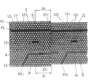
例如,作为这种类型的频率滤器,提出了如14A和14B中所示的电磁波频率滤波器。该电磁波频率滤波器在所谓的板型光子晶体1中,具有线形的输入波导2、输出波导3其设置为在输入波导2的宽度方向上与输入波导2成隔开的关系,以及谐振器4其设置在输入波导2的中间部分和输出波导3的中间部分之间。在图14A和14B中示出的电磁波频率滤波器中,输入波导2和输出波导3的形成是通过在二维的光子晶体1的折射率周期结构中制造两个线形缺陷(即,对折射率周期结构的扰乱)。而谐振器4的形成是通过在在二维的光子晶体1的折射率周期结构中制造一点状缺陷。在板型二维光子晶体1中,在板11的厚度方向上的两侧由高折射率介质例如Si制成,并用均匀的低折射率介质例如空气和SiO2夹入中间,因此电磁波(例如光)被平面中的光子带隙限制并且电磁波在厚度方向上被全反射限制。For example, as this type of frequency filter, electromagnetic wave frequency filters as shown in 14A and 14B are proposed. This electromagnetic wave frequency filter has a
在上面提到的电磁波频率滤波器中,输入波导2的一端定义为端口P1(输入端P1),输入波导2的另一端定义为P2,而输出波导3的一端定义为端口P3(输出端P3),其另一端定义为端口P4。当多个不同频率的电磁波入射到输入端P1时,从该多个电磁波中,匹配谐振器4的谐振频率的预定频率的电磁波,通过谐振器4被传输到输出波导3,然后被从输出端P3输出。具有与谐振器4的谐振频率不同的频率的电磁波被朝向输入波导2的端2传播。在图14A中,实线箭头示出具有与谐振器4的谐振频率相匹配的频率的电磁波的传输路径,而交替长短点划线箭头示出频率与谐振器4的谐振频率不同的电磁波的传播路径。In the electromagnetic wave frequency filter mentioned above, one end of the
上面提到的电磁波频率滤波器可用作光开关,其改变输出端P3的输出并切换对来自输出端P3的电磁波的选取。The above-mentioned electromagnetic wave frequency filter can be used as an optical switch that changes the output of the output terminal P3 and switches selection of electromagnetic waves from the output terminal P3.
顺便说,通过使用模式耦合理论,本发明者评估在图14A、14B中示出的常规电磁波频率滤波器中的从每个端口P1到P4的输出强度以及从谐振器4到自由空间的输出强度,其得到的结果在图15中示出。当应用模式耦合理论时,在谐振器4和输入波导2之间的Q因子定义为Qin而在谐振器4和自由空间之间的Q因子定义为Qv。在图15中,水平轴表示Qin/Qv,而垂直轴表示输出强度,在图15中“X1”表示端P2的输出强度,“X2”表示端P1、P3和P4的输出强度,“X3”表示到自由空间的输出强度。如图15所示,在常规电磁波频率滤波器中,到输出端P3的传输效率的最大值(即波长选择效率)在理论上仅为25%,因此就有传输效率过于不足的问题。另外,Qin是在与谐振器-输入波导系统中从谐振器4漏入到输入波导2中的能量的量有关的一个值。换句话说,Qin是示出在谐振器-输入波导系统中,谐振器4能储存多少能量的一个值。Qin定义如下述表达式:By the way, by using the mode coupling theory, the present inventors evaluated the output intensity from each port P1 to P4 and the output intensity from the
Qin=ω0×W/(-dW/dt)Q in =ω 0 ×W/(-dW/dt)
其中,ω0表示谐振器4的谐振频率,W表示储存在谐振器4中的能量,而(-dW/dt)表示从谐振器4到输入波导2中每单位时间损失的能量。Qv是在谐振器-自由空间系统中与从谐振器4漏入到自由空间中的能量的量有关的一个值。换句话说,Qv是示出在谐振器-自由空间系统中,谐振器4能储存多少能量的一个值。Qv定义如下述表达式:where ω0 denotes the resonant frequency of the
Qv=ω0×W/(-dW/dt)Q v =ω 0 ×W/(-dW/dt)
其中,ω0表示谐振器4的谐振频率,W表示储存在谐振器4中的能量,而(-dW/dt)表示从谐振器4到自由空间中每单位时间损失的能量。where ω0 denotes the resonant frequency of the
另外,已经提出了与图14A和14B示出的电磁波频率滤波器相比而言,能达到较高传输效率的电磁波频率滤波器。该电磁波频率滤波器包括二维光子晶体,其中在二维平面上设置有由具有比空气更高的折射率的介质制成的圆柱形棒,而输入波导、输出波导和两个谐振器形成在该二维光子晶体(例如,看Japanese Kohyo(国家公布的翻译版)No.2001-50887,p.22-23,p.40-46,图3、8和22,及C.Manolatou等人“Couping of Modes Analysis ofResonant Channel Add-Drop Filters”,IEEE JOURNAL QUANTUMELETRONICS,VOL 35,NO 9,1999,p.1322-1331,及Shanhui Fan等人,“Channel Drop Tunneling through Localized States”,PHYSICAL REVIEWLETTERS,VOL 80,NO 5,1998,p.960-963)。In addition, an electromagnetic wave frequency filter capable of achieving higher transmission efficiency compared with the electromagnetic wave frequency filter shown in FIGS. 14A and 14B has been proposed. This electromagnetic wave frequency filter includes a two-dimensional photonic crystal in which a cylindrical rod made of a medium having a higher refractive index than air is arranged on a two-dimensional plane, and an input waveguide, an output waveguide, and two resonators are formed in The two-dimensional photonic crystal (see, for example, Japanese Kohyo (translated version published by the country) No.2001-50887, p.22-23, p.40-46, Figures 3, 8 and 22, and C.Manolatou et al. Couping of Modes Analysis of Resonant Channel Add-Drop Filters", IEEE JOURNAL QUANTUMELETRONICS, VOL 35, NO 9, 1999, p.1322-1331, and Shanhui Fan et al., "Channel Drop Tunneling through Localized States", PHYSICLE REVI0 , NO 5, 1998, p.960-963).
在这种电磁波频率滤波器中,朝向输入波导的输入端的相对端传播的电磁波和朝向输出波导的输出端的相对端传播的电磁波可以被两个谐振器的谐振模式消去。具体的说,两个谐振器构成其中两个谐振器同相振荡的对称模式和两个谐振器反相振荡的反对称模式,当在对称模式中的谐振频率和在反对称模式中的谐振频率彼此相同时,在对称模式中的相对输入波导、输出波导和平面外的自由空间的衰减速率其每一个分别都等于在反对称模式中相对它们的衰减速率,在对称模式的振荡和反对称模式的振荡之间的相位差满足特定条件(例如,π),来自谐振器的在输入波导的输入端(进入端)的相反方向传播的电磁波和来自谐振器的在输出波导的输出端(输出端)的相反方向传播的电磁波可以被消去。因此,可以从仅特定的输出端来选择性地输出电磁波。In this electromagnetic wave frequency filter, an electromagnetic wave propagating toward an end opposite to an input end of an input waveguide and an electromagnetic wave propagating toward an end opposite to an output end of an output waveguide can be canceled by resonance modes of two resonators. Specifically, two resonators constitute a symmetric mode in which the two resonators oscillate in phase and an anti-symmetric mode in which the two resonators oscillate in anti-phase, when the resonant frequency in the symmetric mode and the resonant frequency in the anti-symmetric mode are mutually At the same time, the decay rates relative to the input waveguide, output waveguide, and out-of-plane free space in the symmetric mode are each equal to the decay rates relative to them in the antisymmetric mode, and the oscillations in the symmetric mode and the antisymmetric mode The phase difference between the oscillations satisfies a specific condition (for example, π), the electromagnetic wave from the resonator propagating in the opposite direction at the input end (entry end) of the input waveguide and from the resonator at the output end (output end) of the output waveguide Electromagnetic waves propagating in the opposite direction can be canceled out. Therefore, electromagnetic waves can be selectively output from only a specific output terminal.
顺便提及,在上述的具有两个谐振器的常规电磁波频率滤波器中,可以用下面的方程来计算各在对称模式中的谐振频率ωs和在反对称模式中的谐振频率ωa:Incidentally, in the above-mentioned conventional electromagnetic wave frequency filter having two resonators, each of the resonance frequency ω s in the symmetric mode and the resonance frequency ω a in the antisymmetric mode can be calculated by the following equation:
ωS=ωO-{μ-(1/τe)×sinΦ-(1/τe’)×sinΦ’}ω S =ω O -{μ-(1/τe)×sinΦ-(1/τe')×sinΦ'}
ωa=ωO+{μ-(1/τe)×sinΦ-(1/τe’)×sinΦ’}ω a =ω O +{μ-(1/τe)×sinΦ-(1/τe')×sinΦ'}
其中μ是在谐振器之间不通过任何波导的结合能,Φ是在谐振器通过输入波导相互耦合时在谐振器它们之间的相移量,Φ’是在谐振器通过输出波导相互耦合时在谐振器它们之间的相移量,(1/τe)是从谐振器到输入波导的能量的衰减速率,(1/τe)’是从谐振器到输出波导的能量的衰减速率,ωO是在每个谐振器单独存在的情况下的谐振器频率。从上面的方程中可清楚看到,这些模式的谐振频率ωS、ωa彼此基本不同,因此,为了使两个模式的这些谐振频率ωS、ωa彼此一致,必须要满足下面的条件:where μ is the binding energy between resonators without passing through any waveguide, Φ is the amount of phase shift between the resonators when they are coupled to each other through the input waveguide, and Φ' is the amount of phase shift between the resonators when they are coupled to each other through the output waveguide The amount of phase shift between them in the resonator, (1/τe) is the decay rate of the energy from the resonator to the input waveguide, (1/τe)' is the decay rate of the energy from the resonator to the output waveguide, ω O is the resonator frequency in the case of each resonator alone. It can be clearly seen from the above equation that the resonant frequencies ω s and ω a of these modes are basically different from each other, therefore, in order to make these resonant frequencies ω s and ω a of the two modes coincide with each other, the following conditions must be satisfied:
μ-(1/τe)×sinΦ-(1/τe’)×sinΦ’=0μ-(1/τe)×sinΦ-(1/τe’)×sinΦ’=0
然而,为了满足上面的条件,需要采用复杂的结构。例如,必须将靠近谐振器的棒的折射率设定为与其他棒的折射率不相同的一个值,或者将靠近谐振器的棒的半径设定为与其他棒相比而言为非常小的一个值。因此,有许多设计限制,而难以设计和制造电磁波频率滤波器。However, in order to satisfy the above conditions, it is necessary to adopt a complicated structure. For example, the refractive index of the rod close to the resonator must be set to a value different from that of the other rods, or the radius of the rod close to the resonator must be set to be very small compared to the other rods a value. Therefore, there are many design restrictions, and it is difficult to design and manufacture an electromagnetic wave frequency filter.
发明内容 Contents of the invention
考虑到上述问题,本发明的目的是提供一种电磁波频率滤波器,其能从输入到输入波导中的多个频率的电磁波中从输出波导的输出端选取预定频率的电磁波,并可由较容易的设计来形成。In view of the above problems, the object of the present invention is to provide an electromagnetic wave frequency filter which can select an electromagnetic wave of a predetermined frequency from an output end of an output waveguide from electromagnetic waves of a plurality of frequencies input into an input waveguide, and can be obtained by relatively easy designed to form.
根据本发明的电磁波频率滤波器包括构建为接收输入到输入波导的一端中的多个频率的电磁波的输入波导和与所述输入波导并排设置的输出波导,以及设置在输入波导和输出波导之间的谐振器。该谐振器具有预定的谐振频率并谐振与该谐振频率匹配的预定频率的电磁波以便将电磁波从输入波导传输到输出波导,由此使得从输出波导的一端的输出端发出电磁波。本发明的特征在于输入波导具有输入波导侧的反射器其用于在输入波导的一端的谐振器的相反侧反射该谐振频率电磁波,输出波导具有输出波导侧的反射器其用于在输出波导的一端的相反侧上反射预定频率的电磁波,该电磁波频率滤波器满足下面的关系:An electromagnetic wave frequency filter according to the present invention includes an input waveguide constructed to receive electromagnetic waves of a plurality of frequencies input into one end of the input waveguide and an output waveguide arranged side by side with the input waveguide, and arranged between the input waveguide and the output waveguide the resonator. The resonator has a predetermined resonance frequency and resonates an electromagnetic wave of a predetermined frequency matching the resonance frequency to transmit the electromagnetic wave from the input waveguide to the output waveguide, thereby causing the electromagnetic wave to be emitted from an output end of one end of the output waveguide. The present invention is characterized in that the input waveguide has an input waveguide-side reflector for reflecting the resonant frequency electromagnetic wave on the opposite side of the resonator at one end of the input waveguide, and the output waveguide has an output waveguide-side reflector for reflecting the resonant frequency electromagnetic wave at the side of the output waveguide. Electromagnetic waves of a predetermined frequency are reflected on the opposite side of one end, and the electromagnetic wave frequency filter satisfies the following relationship:
Qinb/(1-cosθ1)《QV Q inb /(1-cosθ 1 )《Q V
Qinb/(1-cosθ2)=Qinr/(1-cosθ2)Q inb /(1-cosθ 2 )=Q inr /(1-cosθ 2 )
θ1、θ2≠2Nπ(N=0,1,...)θ 1 , θ 2 ≠2Nπ (N=0, 1,...)
其中,θ1是被输入波导侧反射器反射而回到谐振器附近的电磁波的相移量,θ2是被输出波导侧反射器反射而回到谐振器附近的电磁波的相移量,Qinb是在谐振器和输入波导之间的Q因子,Qinr是在谐振器和输出波导之间的Q因子,而QV是在谐振器和自由空间之间的Q因子,Qinb是在谐振器-输入波导系统中与从谐振器漏入到输入波导的能量的量有关的一个值。换句话说,Qinb是指示出在谐振器-输入波导系统中谐振器能储存多少能量的一个值。Qinb如下述表达式定义:Among them, θ1 is the phase shift amount of the electromagnetic wave reflected by the reflector on the input waveguide side and returned to the vicinity of the resonator, θ2 is the phase shift amount of the electromagnetic wave reflected by the reflector on the output waveguide side and returned to the vicinity of the resonator, Q inb is the Q factor between the resonator and the input waveguide, Q inr is the Q factor between the resonator and the output waveguide, and Q V is the Q factor between the resonator and free space, Q inb is the Q factor between the resonator - A value in the input waveguide system relating to the amount of energy leaked from the resonator into the input waveguide. In other words, Q inb is a value indicating how much energy a resonator can store in a resonator-input waveguide system. Q inb is defined by the following expression:
Qinb=ω0×W/(-dW/dt)Q inb =ω 0 ×W/(-dW/dt)
其中,ω0表示谐振器的谐振频率,W表示储存在谐振器中的能量,而(-dW/dt)表示从谐振器到输入波导中每单位时间损失的能量。Qinr是在谐振器-输出波导系统中与从谐振器漏入到输出波导中的能量的量有关的一个值。换句话说,Qinr是示出在谐振器-输出波导系统中,谐振器4能储存多少能量的一个值。Qinr定义如下述表达式:where ω0 denotes the resonant frequency of the resonator, W denotes the energy stored in the resonator, and (-dW/dt) denotes the energy lost per unit time from the resonator into the input waveguide. Qinr is a value related to the amount of energy leaked from the resonator into the output waveguide in a resonator-output waveguide system. In other words, Qinr is a value showing how much energy the
Qinr=ω0×W/(-dW/dt)Q inr =ω 0 ×W/(-dW/dt)
其中,ω0表示谐振器的谐振频率,W表示储存在谐振器中的能量,而(-dW/dt)表示从谐振器到输出波导中每单位时间损失的能量。Qv是在谐振器-自由空间系统中与从谐振器漏入到自由空间中的能量的量有关的一个值。换句话说,Qv是示出在谐振器-自由空间系统中,谐振器能储存多少能量的一个值。Qv定义如下述表达式:where ω0 denotes the resonant frequency of the resonator, W denotes the energy stored in the resonator, and (-dW/dt) denotes the energy lost per unit time from the resonator into the output waveguide. Qv is a value related to the amount of energy leaked from the resonator into free space in a resonator-free space system. In other words, Qv is a value showing how much energy a resonator can store in a resonator-free space system. Q v is defined as the following expression:
Qv=ω0×W/(-dW/dt)Q v =ω 0 ×W/(-dW/dt)
其中ω0表示谐振器的谐振频率,W表示储存在谐振器中的能量,而(-dW/dt)表示从谐振器到自由空间中每单位时间损失的能量。然而,每个Qinb、Qinr和QV是由包括输入波导和输出波导的整个系统来决定的。如果在输入波导的一端或者在输出波导的一端有寄生反射部件,或者在输入或输出波导中有寄生谐振部件例如弯曲的波导,每个Qinb、Qinr和QV要考虑这些寄生部件来决定。where ω0 denotes the resonant frequency of the resonator, W denotes the energy stored in the resonator, and (-dW/dt) denotes the energy lost per unit time from the resonator to free space. However, each Q inb , Qinr and Q V is determined by the entire system including the input waveguide and the output waveguide. If there are parasitic reflective components at one end of the input waveguide or at one end of the output waveguide, or parasitic resonant components such as curved waveguides in either the input or output waveguide, each Q inb , Qinr and Q V are determined taking these parasitic components into account .
本发明的电磁波频率滤波器能有效地从入射到输入波导上的多个频率的电磁波中,从输出波导的输出端选取匹配谐振器的谐振频率的预定频率的电磁波,并可由较容易的设计来形成。对电磁波频率滤波器来说可达到接近100%的传输效率。The electromagnetic wave frequency filter of the present invention can effectively select the electromagnetic wave of the predetermined frequency matching the resonant frequency of the resonator from the output end of the output waveguide from the electromagnetic waves of a plurality of frequencies incident on the input waveguide, and can be obtained by easier design. form. For electromagnetic frequency filters, a transmission efficiency close to 100% can be achieved.
优选地,该电磁波频率滤波器具有面内异质结构,在该异质结构中至少具有在二维面上的折射率周期结构的第一光子晶体和具有周期与第一光子晶体的折射率周期结构不同的折射率周期结构的第二光子晶体,被并排放置在同一面内,输入波导的形成是通过在这些光子晶体的排列方向上沿整个长度上在第一和第二光子晶体的折射率周期结构中制造线形缺陷,而输出波导的形成是通过在这些光子晶体的排列方向上跨着这些光子晶体在第一和第二光子晶体的折射率周期结构中制造线形缺陷,而谐振器的形成是通过在第一光子晶体中制造点状缺陷,谐振器的谐振频率包括在第二光子晶体不具有波导模式中的频带中,输入波导侧反射器由在输入波导形成在第一光子晶体中的一部分和输入波导形成在第二光子晶体中的一部分之间的边界形成,而输出波导侧反射器由在输出波导形成在第一光子晶体中的一部分和输出波导形成在第二光子晶体中的一部分之间的边界形成。Preferably, the electromagnetic wave frequency filter has an in-plane heterostructure in which there is at least a first photonic crystal with a periodic refractive index structure on a two-dimensional plane and a photonic crystal having a period equal to that of the first photonic crystal. Second photonic crystals with different refractive index periodic structures are placed side by side in the same plane, and the input waveguide is formed by changing the refractive index of the first and second photonic crystals along the entire length in the direction of arrangement of these photonic crystals. The formation of linear defects in the periodic structure, while the output waveguide is formed by making linear defects in the refractive index periodic structures of the first and second photonic crystals across the photonic crystals in the alignment direction of these photonic crystals, and the formation of the resonator By making a point-like defect in the first photonic crystal, the resonant frequency of the resonator is included in the frequency band in which the second photonic crystal does not have a waveguide mode, and the input waveguide side reflector is formed by the input waveguide in the first photonic crystal A part of the boundary between the input waveguide and the part formed in the second photonic crystal, and the output waveguide side reflector is formed by the part of the output waveguide formed in the first photonic crystal and the part of the output waveguide formed in the second photonic crystal The boundary between them is formed.
在这种情况中,谐振频率的电磁波可通过使用该面内异质结构而被反射。In this case, electromagnetic waves of the resonance frequency can be reflected by using the in-plane heterostructure.
最好,第一光子晶体和第二光子晶体其每一个为二维光子晶体,而在谐振器和输入波导之间的间隙与在谐振器和输出波导之间的间隙设定为彼此相等,在谐振器和输入波导侧反射器之间沿输入波导方向上的距离d1与在谐振器和输出波导侧反射器之间沿输出波导方向上的距离d2设定为彼此相等(d1=d2),且输入波导的传播常数β1与输出波导的传播常数β2设定为彼此相等(β1=β2),在输入波导形成在第一二维光子晶体中的部分和输入波导形成在第二二维光子晶体中的部分之间的轴错位量与输出波导形成在第一二维光子晶体中的部分和输出波导形成在第二二维光子晶体中的部分之间的轴错位量设定为彼此相等,以使被输入波导侧的反射器反射的电磁波的反射相移Δ1与被输出波导侧的反射器反射的电磁波的反射相移Δ2彼此相等(Δ1=Δ2)。Preferably, each of the first photonic crystal and the second photonic crystal is a two-dimensional photonic crystal, and the gap between the resonator and the input waveguide and the gap between the resonator and the output waveguide are set to be equal to each other, in The distance d1 between the resonator and the reflector on the input waveguide side in the direction of the input waveguide and the distance d2 between the resonator and the reflector on the output waveguide side along the direction of the output waveguide are set to be equal to each other ( d1 =d 2 ), and the propagation constant β 1 of the input waveguide and the propagation constant β 2 of the output waveguide are set to be equal to each other (β 1 = β 2 ), the part where the input waveguide is formed in the first two-dimensional photonic crystal and the input waveguide is formed The amount of axial misalignment between the portions in the second two-dimensional photonic crystal and the axial misalignment amount between the portion where the output waveguide is formed in the first two-dimensional photonic crystal and the portion where the output waveguide is formed in the second two-dimensional photonic crystal Set to be equal to each other so that the reflection phase shift Δ1 of the electromagnetic wave reflected by the reflector on the input waveguide side and the reflection phase shift Δ2 of the electromagnetic wave reflected by the reflector on the output waveguide side are equal to each other ( Δ1 = Δ2 ) .
在这种情况中,θ1=θ2,传输效率关于θ1和θ2的波动的波动范围较小,因此可增大对θ1和θ2的波动的容许量。In this case, θ 1 =θ 2 , the fluctuation range of the transmission efficiency with respect to fluctuations in θ 1 and θ 2 is small, and thus the allowable amount for fluctuations in θ 1 and θ 2 can be increased.
最好,在靠近第一光子晶体和第二光子晶体之间的边界处,至少第一二维光子晶体和第二二维光子晶体其中之一的折射率周期结构的周期阶段性地改变使得输入波导平滑且连续地延伸而邻近所述边界。Preferably, near the boundary between the first photonic crystal and the second photonic crystal, the period of the refractive index periodic structure of at least one of the first two-dimensional photonic crystal and the second two-dimensional photonic crystal changes stepwise such that the input The waveguide extends smoothly and continuously adjacent to the boundary.
在这种情况中,因为输入波导平滑且连续地延伸而邻近在第一光子晶体和第二光子晶体之间的边界,因输入波导的轴错位而产生的,频率与形成在第一光子晶体中的谐振器的谐振频率不同的电磁波的反射损失可以被减小。In this case, since the input waveguide extends smoothly and continuously adjacent to the boundary between the first photonic crystal and the second photonic crystal, due to the axis misalignment of the input waveguide, the frequency and The reflection loss of electromagnetic waves different from the resonant frequency of the resonator can be reduced.
另外最好,第一光子晶体和第二光子晶体在输入波导和输出波导的排列方向上的相对位置被设定为使得在第一光子晶体和第二光子晶体之间不会产生输入波导的轴错位,且输入波导侧反射器和谐振器之间的距离设定为满足cosθ1=cosθ2的关系。Also preferably, the relative positions of the first photonic crystal and the second photonic crystal in the arrangement direction of the input waveguide and the output waveguide are set so that no axis of the input waveguide is generated between the first photonic crystal and the second photonic crystal. misalignment, and the distance between the input waveguide side reflector and the resonator is set to satisfy the relationship of cosθ 1 =cosθ 2 .
在这种情况中,因输入波导的轴错位而产生的,频率与所述谐振频率不同的电磁波的反射损失可以被消除。In this case, reflection loss of an electromagnetic wave having a frequency different from the resonant frequency due to axis misalignment of the input waveguide can be eliminated.
或者,同样优选地,第一光子晶体和第二光子晶体在输入波导和输出波导的排列方向上的相对位置被设定为使得在第一光子晶体和第二光子晶体之间不会产生输入波导的轴错位,且在输出波导侧反射器上设置用于将Δ2与Δ1匹配的相位补偿器。Or, also preferably, the relative positions of the first photonic crystal and the second photonic crystal in the arrangement direction of the input waveguide and the output waveguide are set so that no input waveguide is generated between the first photonic crystal and the second photonic crystal. The axis of Δ is misaligned, and a phase compensator for matching Δ 2 to Δ 1 is provided on the output waveguide side reflector.
在这种情况中,可以将输出波导侧的反射器的反射效率与输入波导侧的反射器的反射效率相匹配,由此可以增大对距离d1和d2的变化的容许量。In this case, the reflective efficiency of the reflector on the output waveguide side can be matched to that of the reflector on the input waveguide side, whereby the tolerance for variations in the distances d1 and d2 can be increased.
同样优选地,该电磁波频率滤波器具有面内异质结构,在该异质结构中至少具有在二维面内的折射率周期结构的第一光子晶体和具有其周期与该第一光子晶体的折射率周期结构不同的折射率周期结构的第二光子晶体被并排放置在同一平面中,输入波导的形成是通过在这些光子晶体的排列方向上沿整个长度上在第一和第二光子晶体的折射率周期结构中制造线形缺陷,而谐振器的形成是通过在第一光子晶体中制造点状缺陷,而输出波导的形成是通过在第一光子晶体的折射率周期结构中制造线形缺陷,而输出波导的相反端构成输出波导侧反射器。Also preferably, the electromagnetic wave frequency filter has an in-plane heterostructure in which at least a first photonic crystal having a periodic structure of refractive index in a two-dimensional plane and a photonic crystal having a period identical to that of the first photonic crystal Second photonic crystals with different refractive index periodic structures are placed side by side in the same plane, and the input waveguide is formed by forming the first and second photonic crystals along the entire length in the arrangement direction of these photonic crystals. Create linear defects in the refractive index periodic structure, and the resonator is formed by making point defects in the first photonic crystal, and the output waveguide is formed by making linear defects in the refractive index periodic structure of the first photonic crystal, and The opposite end of the output waveguide constitutes the output waveguide side reflector.
在这种情况中,在输入波导中,通过使用该面内异质结构来反射谐振频率的电磁波,而在输出波导中,通过使用在输出波导的相反端的第一二维光子晶体的光子带隙来反射谐振频率的电磁波。In this case, in the input waveguide, by using this in-plane heterostructure to reflect electromagnetic waves at the resonant frequency, and in the output waveguide, by using the photonic bandgap of the first two-dimensional photonic crystal at the opposite end of the output waveguide to reflect electromagnetic waves at the resonant frequency.
在上述情况中,最好第一光子晶体和第二光子晶体其每一个为二维光子晶体,所述谐振器和所述输入波导侧的反射器在沿所述输入波导方向上的距离d1与所述谐振器和所述输出波导侧的反射器在沿所述输出波导方向上的距离d2设定为满足cosθ1=cosθ2的关系。In the above case, it is preferable that each of the first photonic crystal and the second photonic crystal is a two-dimensional photonic crystal, and the distance d between the resonator and the reflector on the input waveguide side in the direction along the input waveguide is d1 A distance d 2 in the direction along the output waveguide from the resonator and the reflector on the output waveguide side is set to satisfy the relationship of cosθ 1 =cosθ 2 .
在这种情况中,设计电磁波频率滤波器就变得容易。In this case, it becomes easy to design an electromagnetic wave frequency filter.
最好,第一光子晶体的折射率周期结构变化为使得靠近输出波导的相反端的电磁场分布不会急遽变化。Preferably, the periodic structure of the refractive index of the first photonic crystal is changed such that the electromagnetic field distribution near the opposite end of the output waveguide does not change abruptly.
在这种情况中,可以防止靠近输出波导的相反端的电磁场分布急遽变化,从而可以降低到自由空间的辐射损失,因而提高传输效率。In this case, the electromagnetic field distribution near the opposite end of the output waveguide can be prevented from abruptly changing, so that radiation loss to free space can be reduced, thereby improving transmission efficiency.
优选地,电磁波频率滤波器设计为使得Qinb、Qinr、cosθ1和cosθ2满足下述关系:Qinb=Qinr和cosθ1=cosθ2。Preferably, the electromagnetic wave frequency filter is designed such that Qinb , Qinr , cosθ 1 and cosθ 2 satisfy the following relationships: Qinb =Q inr and cosθ 1 =cosθ 2 .
在这种情况中,可以在关于谐振器的对称结构中,即在谐振器和输入波导之间的距离与谐振器和输出波导之间的距离设定为彼此相等,提高传输效率,因此滤波器的设计就变得容易。In this case, the transmission efficiency can be improved in a symmetrical structure about the resonator, that is, the distance between the resonator and the input waveguide and the distance between the resonator and the output waveguide are set to be equal to each other, so the filter design becomes easy.
同样优选地,电磁波频率滤波器还包括一控制装置其用于通过改变靠近至少输入波导侧的反射器和输出波导侧的反射器其中之一的折射率来改变输出端的输出,或者一控制装置其用于通过改变靠近至少输入波导侧的反射器和输出波导侧的反射器其中之一的折射率周期结构的周期来改变输出端的输出,或者一控制装置其用于通过改变靠近各输入和输出波导反射器及谐振器的折射率来改变输出端的输出。Also preferably, the electromagnetic wave frequency filter further includes a control device for changing the output at the output end by changing the refractive index of at least one of the reflector on the input waveguide side and the reflector on the output waveguide side, or a control device whose for changing the output at the output end by changing the period of the refractive index periodic structure near at least one of the reflector on the input waveguide side and the reflector on the output waveguide side, or a control means for changing the period of the refractive index periodic structure near each of the input and output waveguides The refractive index of the reflector and the resonator is used to change the output at the output terminal.
在这些情况中,该电磁波频率滤波器可用作频率选择(波长选择)电磁波开关。In these cases, the electromagnetic wave frequency filter can be used as a frequency selective (wavelength selective) electromagnetic wave switch.
Qinb≠Qinr也同样优选,该电磁波频率滤波器还包括一控制装置,其通过改变靠近输出波导侧的反射器的折射率来改变输出端的输出。It is also preferable that Q inb ≠Q inr , the electromagnetic wave frequency filter further includes a control device, which changes the output at the output end by changing the refractive index of the reflector near the output waveguide side.
在这种情况中,该电磁波频率滤波器可用作频率选择(波长选择)电磁波开关,另外,因为传输效率响应θ2的改变的量而改变的量被增大,可以减小能耗量的量并使开关速度更快。In this case, the electromagnetic wave frequency filter can be used as a frequency selective (wavelength selective) electromagnetic wave switch, and in addition, since the amount of change in transmission efficiency in response to the amount of change in θ2 is increased, the amount of energy consumption can be reduced amount and make switching faster.
附图说明 Description of drawings
图1示出本发明第一实施例的示意图;Fig. 1 shows the schematic diagram of the first embodiment of the present invention;
图2示出第一实施例的特性评估图示;Fig. 2 shows a characteristic evaluation diagram of the first embodiment;
图3示出本发明第二实施例的平面示意图;Fig. 3 shows a schematic plan view of a second embodiment of the present invention;
图4示出本发明第三实施例的平面示意图;Fig. 4 shows a schematic plan view of a third embodiment of the present invention;
图5示出第三实施例的特性评估图示;Fig. 5 shows a characteristic evaluation diagram of the third embodiment;
图6示出第三实施例的另一结构的平面示意图;Fig. 6 shows a schematic plan view of another structure of the third embodiment;
图7示出本发明第四实施例的平面示意图;Fig. 7 shows a schematic plan view of a fourth embodiment of the present invention;
图8示出第四实施例的特性评估图示;FIG. 8 shows a characteristic evaluation diagram of the fourth embodiment;
图9A示出本发明第五实施例的平面示意图而图9B示出图9A一实质部分的放大图;9A shows a schematic plan view of a fifth embodiment of the present invention and FIG. 9B shows an enlarged view of a substantial part of FIG. 9A;
图10示出本发明第六实施例的平面示意图;Fig. 10 shows a schematic plan view of a sixth embodiment of the present invention;
图11示出第六实施例的特性评估图示;FIG. 11 shows a characteristic evaluation diagram of the sixth embodiment;
图12示出本发明第七实施例的平面示意图;Fig. 12 shows a schematic plan view of a seventh embodiment of the present invention;
图13示出第七实施例的特性评估图示;FIG. 13 shows a characteristic evaluation diagram of the seventh embodiment;
图14A示出常规结构的平面示意图,而图14B示出图14A的一实质部分的放大图;Figure 14A shows a schematic plan view of a conventional structure, while Figure 14B shows an enlarged view of a substantial portion of Figure 14A;
图15示出图14A的特性评估图示。Fig. 15 shows the characteristic evaluation diagram of Fig. 14A.
具体实施方式 Detailed ways
以下,将参考附图来具体描述本发明。Hereinafter, the present invention will be specifically described with reference to the accompanying drawings.
第一实施例first embodiment
如图1所示,该实施例的电磁波频率滤波器具有面内异质结构,其中其每个具有彼此不同的折射率周期结构的多个二维光子晶体11,12,...,被并排放置在二维平面的一个方向(图1的水平方向)上(在图1中仅示出了两个二维光子晶体11,12)。该电磁波频率滤波器具有输入波导2,该波导的形成是通过在所有二维光子晶体11,12,...的折射率周期结构中在二维光子晶体11,12,...,的排列方向上沿二维光子晶体的整个长度上制造一线形缺陷。该电磁波频率滤波器还具有输出波导31,32,...,其每一个的形成是通过在每对彼此相邻的二维光子晶体1n,1m(n=1,2,...,m=n+1)的折射率周期结构中在这些二维光子晶体11,12,...排列方向上制造线形缺陷,使得该线形缺陷跨过每对二维光子晶体1n,1m。该电磁波频率滤波器还具有谐振器41,42,...,其每一个的形成是通过在每对二维光子晶体1n,1m中的一个二维光子晶体1n的折射率周期结构中制造点状缺陷。输入波导2的一端(图1的左端)被定义为输入端P1,而每个输出波导31,32,...的一端(图1的左端)被分别定义为输出端P31,P32,...。As shown in FIG. 1 , the electromagnetic wave frequency filter of this embodiment has an in-plane heterostructure each of which has a plurality of two-
每个输出波导31,32,...设置为与输入波导2并排,而每个谐振器41,42,...设置在输入波导2和每个输出波导31,32,...的中间部分之间,每个谐振器具有谐振频率ω01,ω02,...。在该电磁波频率滤波器中,当多个频率的电磁波入射到输入端P1时,从该多个频率的电磁波中与每个谐振频率ω01,ω02,...相匹配的预定频率的电磁波被从输入波导2通过每个谐振器41,42,...传输到每个输出波导31,32,...并从每个输出波导31,32,...的输出端P31,P32,...输出。谐振器41,42,...的每个谐振频率ω01,ω02,...与其他的不同,例如频率(第一预定频率)与谐振器41的谐振频率ω01相匹配的电磁波通过谐振器41被从输出波导31的输出端P31输出(发出),而频率(第二预定频率)与谐振器42的谐振频率ω02相匹配的电磁波通过谐振器42被从输出波导32的输出端P32输出(发出)。每个输出波导31,32,...的中间部分与输入波导2平行。Each output
每个二维光子晶体11,12,...是所谓的板型二维光子晶体,其包括由高折射率介质例如Si和夹在该高折射率介质的厚度方向的两侧的均匀的低折射率介质例如空气和SiO2制成的板111,112,...。在二维光子晶体的面内,光被光子带隙限制,在厚度方向上,光被全反射限制。在每个二维光子晶体11,12,...中排列了多个圆孔121,122,...以在垂直板111,112,...的厚度方向的平面内具有二维周期结构,构成板111,112,...的高折射率介质与在圆孔121,122,...中作为低折射率介质的空气构成具有折射率周期结构的二维光子晶体11,12,...。具体的说,每个光子晶体11,12,...的形成是通过在每个板111,112,...中在单元格为正三角形的假想二维三角形点阵的每个格点上制造圆孔121,122,...。换句话说,圆孔121,122,...排列为三角形格形式,在与每个111,112,...的厚度方向相垂直的平面上。Each two-
在该实施例的电磁波频率滤波器中,每对二维光子晶体11,12,...的折射率周期结构具有比例关系,在二维光子晶体1m中在圆孔12m(m=n+1,n=1,2,...)的排列方向上的周期设定为比在在二维光子晶体1n中在圆孔12n(n=1,2,...)的排列方向上的周期小几个百分比(例如1.2%)以便通过使用每对二维光子晶体1n,1m形成面内异质结构。In the electromagnetic frequency filter of this embodiment, the periodic structures of the refractive index of each pair of two-
更具体的说,在该实施例中,光学通讯波长范围例如C波段(1530nm-1565nm)和L波段(1565nm-1625nm)被假定为要输入到输入端P1的电磁波的频率波段。在二维光子晶体11中在圆孔121的排列方向上的周期(a1)设定为0.42μm,每个圆孔121的半径设定为0.29a1,而板111的厚度设定为0.6a1。在放在二维光子晶体11旁边的光子晶体12中,每个圆孔122的半径和板112的厚度等于二维光子晶体11的,而在圆孔122的的排列方向上的周期(a2)(换句话说,二维光子晶体12的折射率周期结构的周期,其为在二维三角形点阵的格点之间的距离)被设定为比二维光子晶体11的圆孔121的周期a1小1.2%。通过将在圆孔121、122的排列方向上的周期a1、a2设定为这样的值,可以形成光子带隙,该光子带隙为一波长范围在该范围中从二维面内各个方向入射来的任何在上述频带中的电磁波(光)都不能传播。输入波导2,输出波导31,32,...以及谐振器41,42,...,其每一个的形成是通过略过适当数目的圆孔121,122,...。在该实施例中,虽然每个输出波导31,32,...具有弯曲部分,因为光在光子带隙的静态传播在二维光子晶体11,12,...中二维面内的所有方向上被限制,所以电磁波可以在输出波导中没有辐射损失而传播。圆孔121、122的周期a1、a2的值以及每个圆孔121、122的半径并不特别限于这些值。每个周期a1、a2可以是在上述频带中的电磁波的波长的同量级的周期(例如,其约为电磁波波长的一半)。More specifically, in this embodiment, optical communication wavelength ranges such as C-band (1530nm-1565nm) and L-band (1565nm-1625nm) are assumed as frequency bands of electromagnetic waves to be input to the input terminal P1. The period (a 1 ) in the arrangement direction of the
在该实施例中,假定使用在上面提到的光学通讯波长范围中的电磁波,电磁波频率滤波器的形成是通过使用所谓的SOI(silicon on insulator)基底,其在厚度方向的中间部分具有为绝缘膜的二氧化硅膜(植入的二氧化物膜)。在该实施例的电磁波频率滤波器中的二维光子晶体11,12,...、输入波导2、输出波导31,32,...和谐振器41,42,...的形成是通过使用光刻技术和蚀刻技术加工SOI基底的主表面侧的硅层。因此可以比较容易地形成二维光子晶体11,12,...、输入波导2、输出波导31,32,...和谐振器41,42,...。例如,在商业SOI晶片的主表面侧的硅层上形成构图成预期形状的保护层,然后用干蚀刻机器蚀刻该硅层使得保留对应输入波导2、输出波导31,32,...和谐振器41,42,以及板111,112,...的部分而除去对应圆孔121,122,...的部分。结果,可以同时形成二维光子晶体11,12,...、输入波导2、输出波导31,32,...和谐振器41,42,...。在C波段和L波段等等的光学通讯波长范围中,Si的折射率约为3.4,SiO2的折射率约为1.5而空气为1,因此在板111,112,...和在其两侧的覆层的相对折射率差异为55-70%,与在典型光纤中芯与覆层之间的相对折射率差异(0.3%)相比,这是一个非常大的值。因而,与光纤相比,可以增强光限制效果,可以使滤波器小型化。In this embodiment, assuming that electromagnetic waves in the above-mentioned optical communication wavelength range are used, the electromagnetic wave frequency filter is formed by using a so-called SOI (silicon on insulator) substrate having an insulating Silicon dioxide membrane of the membrane (implanted dioxide membrane). Two-
如上面提到的那样,在该实施例的电磁波频率滤波器中,由每对二维光子晶体1n,1m形成面内异质结构,而形成为跨过该对二维光子晶体1n,1m的输入波导2和输出波导3n(n=1,2,..)的波导模式在二维光子晶体1n,1m中是不同的。因而,在传播通过形成在二维光子晶体1n中的波导2、3n的部分的多个频率中的一些频率,不能传播通过形成在二维光子晶体1m中的波导2、3n的部分,并且它们被反射。谐振频率被设定为与被反射的频率相匹配。就是说,在该实施例的电磁波频率滤波器中,形成在二维光子晶体1n中的谐振器4n(n=1,2,..)的谐振频率包括在二维光子晶体1m中具有无波导模式的频带中,在二维光子晶体1n,1m之间的边界的附近,用于反射具有与形成在二维光子晶体1n中的谐振器4n(n=1,2,..)的谐振频率相匹配的频率的电磁波的输入波导侧反射器21n(n=1,2,..),由形成在二维光子晶体1n(以下称为前侧二维光子晶体1n)中的输入波导2的部分和形成在二维光子晶体1m(以下称为后侧二维光子晶体1m)中的输入波导2的部分之间的边界来形成,而用于反射具有与谐振器4n(n=1,2,..)的谐振频率相匹配的频率的电磁波的输出波导侧反射器31n(n=1,2,..),由形成在前侧二维光子晶体1n中的输出波导31的部分和形成在后侧二维光子晶体1m中的输出波导3的部分之间的边界来形成。As mentioned above, in the electromagnetic wave frequency filter of this embodiment, an in-plane heterostructure is formed by each pair of two-
就是说,在本实施例的电磁波频率滤波器中,输入波导2的一端定义为输入端P1,每个输出波导31,32,...的一端分别定义为输出端P31,P32,...,用于反射每个谐振器41,42,...的谐振频率的电磁波的输入波导侧反射器211...设置在输入波导2上在输入波导2自每个谐振器41,42,...的一端的相反侧,而用于反射每个谐振器41,42,...的谐振频率的电磁波的输出波导侧反射器311...设置在每个输出波导31,32,...的相反侧,因此,在本实施例的电磁波频率滤波器中,从输入波导2通过每个谐振器41,42,...传输到每个输出波导31,32,...,并朝每个输出波导31,32,...的输出端P31,P32,...的相反端传播的电磁波被每个输出波导侧反射器311...反射,而电磁波其从输入波导2传输到每个谐振器41,42,...然后回到输入波导2然后朝向输入波导2的输入端P1的相反端传播,以及电磁波其匹配每个谐振器41,42,...的谐振频率并朝向输入波导2的相反端传播而没有被传输到每个谐振器41,42,...上,被每个输入波导侧反射器211...反射。在图1中,交替的长短点划线的箭头示出频率与谐振器41,42,...的谐振频率不同的电磁波的传播路径,而实线箭头示出频率与谐振器41的谐振频率相匹配的电磁波的传输路径的例子,该电磁波的传输路径为被输入波导侧反射器211反射并通过谐振器41移到输出波导31并被输出波导侧反射器311反射,然后从输出端31输出。That is to say, in the electromagnetic wave frequency filter of this embodiment, one end of the
在本实施例的电磁波频率滤波器中,当在谐振器41和输入波导侧反射器211之间在沿输入波导2的方向上的距离表示为d1,在谐振器41和输出波导侧反射器311之间在沿输出波导31的方向上的距离表示为d2,输入波导2的传播常数表示为β1,输出波导31的传播常数表示为β2,被输入波导侧反射器211反射的电磁波的反射相移表示为Δ1,被输出波导侧反射器311反射的电磁波的反射相移表示为Δ2,被输入波导侧反射器211反射并回到靠近谐振器41的电磁波的相移量表示为θ1,被输出波导侧反射器311反射并回到靠近谐振器41的电磁波的相移量表示为θ2,各相移量θ1和θ2由下面的方程计算:In the electromagnetic wave frequency filter of the present embodiment, when the distance between the
θ1=2β1×d1+Δ1 θ 1 =2β 1 ×d 1 +Δ 1
θ2=2β2×d2+Δ2 θ 2 =2β 2 ×d 2 +Δ 2
另外可以使用模式耦合理论来计算输出端P31的传输效率D,其由下面的方程表达:In addition, the mode coupling theory can be used to calculate the transmission efficiency D of the output P3 1 , which is expressed by the following equation:
[方程1][equation 1]
其中,Qinb是谐振器41和输入波导2之间的Q因子,Qinr是谐振器41和输入波导31之间的Q因子,ω是电磁波的频率,ω0是谐振器41的谐振频率,S+1是在通过输入端P1输入到输入波导2中的多个电磁波中匹配谐振器41的谐振频率的预定频率的电磁波的振幅,而S-3是从输出端P31输出的电磁波的振幅。Where, Q inb is the Q factor between
在上述方程中,因为本实施例的电磁波频率滤波器的谐振器41的形成是通过在板型二维光子晶体11中的折射率周期结构中制造缺陷,而该缺陷为所谓的施主型缺陷,即该缺陷的形成是通过向在折射率周期结构中预期要形成圆孔121的位置上的二维光子晶体11的部分中加入半导体材料(在本实施例中,该施主型缺陷的形成是通过向两个圆孔121中加入Si),对自由空间的辐射损失较低并能获得高的QV(Qinb/(1-cosθ1)《QV)。这样,在上述方程中的1/QV可忽略为0。因此,当每个参数d1、d2、β1、β2、Δ1、Δ2、θ1、θ2、Qinb、Qinr和QV设定为满足下面的条件时:In the above equation, because the resonator 41 of the electromagnetic wave frequency filter of this embodiment is formed by making a defect in the refractive index periodic structure in the plate-type two-dimensional photonic crystal 11 , and the defect is a so-called donor type defect, that is, the defect is formed by adding a semiconductor material (in this embodiment, the donor - type defect is formed by adding Si) into the two circular holes 12 1 ), the radiation loss to free space is low and a high Q V (Q inb /(1-cosθ 1 )<Q V ) can be obtained. Thus, 1/Q V in the above equation can be ignored as zero. Therefore, when each parameter d 1 , d 2 , β 1 , β 2 , Δ 1 , Δ 2 , θ 1 , θ 2 , Qinb , Qinr , and Q V is set to satisfy the following conditions:
Qinb/(1-cosθ1)=Qinr/(1-cosθ2)Q inb /(1-cosθ 1 )=Q inr /(1-cosθ 2 )
θ1、θ2≠2Nπ(N=0,1,...)θ 1 , θ 2 ≠2Nπ (N=0, 1,...)
传输效率D可接近1,即接近100%。就是说,与常规滤波器相比,对本实施例的电磁波频率滤波器可以用较容易的设计来提高传输效率。另外,由例如出版物(Y.Akahane等人,Great improvement of Q-factor by shifting latticepoints of a two-dimensional photonic crystal slab point defect resonator(日语),Extended Abstracts of the 50th Japan society of Applied Physics and RelatedSocieties,29a-YN-9(2003,三月)),以及出版物(Y.Akahane等人,Design ofchannel drop filter by using a donor-type cavity with high-quality factor in atwo-dimensional photonic crystal slab,APPLIED PHYSICS LETTERS,VOL.82,NO.9,2003,p.1341-1343),报告了通过在具有高Q因子QV的二维光子晶体中制造施主型缺陷而形成的谐振器。在前者中,报道说可得到45000的QV,而在后者中,报道说可得到5000的QV。The transmission efficiency D can be close to 1, ie close to 100%. That is, compared with the conventional filter, the electromagnetic wave frequency filter of the present embodiment can be designed more easily to improve the transmission efficiency. In addition, from publications such as (Y. Akahane et al., Great improvement of Q-factor by shifting lattice points of a two-dimensional photonic crystal slab point defect resonator (Japanese), Extended Abstracts of the 50 th Japan society of Applied Physics and Related Societies , 29a-YN-9 (2003, March)), and publications (Y.Akahane et al., Design of channel drop filter by using a donor-type cavity with high-quality factor in two-dimensional photonic crystal slab, APPLIED PHYSICS LETTERS, VOL.82, NO.9, 2003, p.1341-1343), reported a resonator formed by fabricating donor-type defects in a two-dimensional photonic crystal with a high Q factor QV . In the former, it was reported that a Q V of 45,000 was obtained, while in the latter, a Q V of 5,000 was reported to be obtained.
在本实施例的电磁波频率滤波器中,谐振器41,42,...的位置设定为使得所有的谐振器41,42,...排列在沿二维光子晶体11,12,...的排列方向上行进的直线上,而在每个谐振器和输入波导2之间的距离以及在每个谐振器和每个输出波导之间的距离被设定为彼此相等,以使Q因子Qinb和Qinr彼此相等(Qinb=Qinr)。此外,通过设定d1=d2,Δ1=Δ2和β1=β2,将相移量θ1和θ2设定为相等(θ1=θ2)。这样因为cosθ1=cosθ2,相移量θ1、θ2和传输效率D具有图2示出的关系。在图2中,水平轴表示相移量θ1,而垂直轴表示相移量θ2,而传输效率D由灰阶的等高线表示,其中颜色接近黑色则传输效率变得越低而颜色接近白色则其变得越高。在本实施例的电磁波频率滤波器中,通过将在输入波导2的形成在二维光子晶体11中的部分与输入波导2的形成在二维光子晶体12中的部分之间的轴错位量,与在输出波导31的形成在二维光子晶体11中的部分与输出波导31的形成在二维光子晶体12中的部分之间的输出波导31的轴错位量,设定为彼此相等,而将反射相移Δ1和Δ2设定为彼此相等(Δ1=Δ2)。因此,θ1=θ2,则相移量θ1、θ2沿着短划线L响应距离d1(=d2)的变化而变化,因而,对于相移量θ1、θ2的波动的传输效率(即波长选择效率)的波动范围较小,可以增大对相移量θ1、θ2的波动的容许量。In the electromagnetic wave frequency filter of this embodiment, the positions of the
应注意到,虽然上述方程1是用于求解输出端P31的传输效率的方程,可以对其他输出端P32,...建立同样关系的表达式。It should be noted that although the above-mentioned
如上面提到的那样,在本实施例的电磁波频率滤波器中,当在输入到输入波导2中的多个频率的电磁波中匹配每个谐振器41,42,...的谐振频率的预定频率的电磁波被从输出波导31,32,...的每个输出端P31,P32,...中选出时,与常规电磁波频率滤波器相比,可以提高传输效率(波长选择效率)。另外,因为在关于谐振器41,42,...的对称结构中即在每个谐振器41,42,...和输入波导2之间的距离与在每个谐振器41,42,...和每个输出波导31,32,...之间的距离被设定为相等时,可以增大传输效率,对电磁波频率滤波器的设计较为容易。As mentioned above, in the electromagnetic wave frequency filter of the present embodiment, when matching the resonance frequency of each
虽然在本实施例中采用Si作为构成二维光子晶体11,12,...的板111,112,...的高折射率介质,其并不限于Si,而是可以是其他材料,例如GaAs、InP。Although Si is used as the high-refractive-index medium constituting the
[第二实施例][Second embodiment]
在第一实施例的电磁波频率滤波器中,谐振器41,42,...被设置为使得所有的谐振器41,42,...排列在一直线上,而在这些二维光子晶体11,12,...的排列方向上的彼此相邻的每对二维光子晶体1n,1m(n=1,2,...,m=n+1)中的折射率周期结构中的周期彼此不同。这样,输入波导2在输入波导形成在前二维光子晶体1n(在图1中,在二维光子晶体11中)的部分与输入波导2在输入波导形成在后二维光子晶体1m(在图1中,在二维光子晶体12中)的部分之间,具有轴错位(光轴的错位)。结果是,对频率与谐振器4n(在图1中,谐振器41)的谐振频率不同的电磁波,会产生因输入波导2的轴错位引起的反射损失,由此,在多个输出端P31,P32,...沿输入波导2的纵向方向排列的情况中,后面的输出端P32,...的传输效率(波长选择效率)随着对输出端P31的接近程度的下降而变得更低。In the electromagnetic wave frequency filter of the first embodiment, the
与之相比,在本实施例中,如图3所示,在二维光子晶体11,12,...的排列方向上的彼此相邻的每对二维光子晶体1n,1m(n=1,2,...,m=n+1)的边界附近,前二维光子晶体1n(在图1中,在二维光子晶体11中)和后二维光子晶体1m(在图1中,在二维光子晶体12中)两者的折射率周期结构的周期都阶段性改变,使得输入波导2平滑并连续地延伸而靠近边界。本实施例的电磁波频率滤波器的基本结构与第一实施例的相同,因此,与第一实施例相似的零件用相同的附图标记来标示,并且这里不再进行重复说明。In contrast, in this embodiment, as shown in FIG. 3 , each pair of two-
在本实施例的电磁波频率滤波器中,因为输入波导2平滑且连续地延伸而靠近在多个二维光子晶体11,12,...的排列方向上的彼此相邻的每对二维光子晶体1n,1m(n=1,2,...,m=n+1)的边界,对频率与形成在前二维光子晶体1n中的谐振器4n的谐振频率不同的电磁波,因输入波导2的轴错位引起的反射损失可以被减小,由此,与第一实施例相比,可以增大后面的输出端P32,...的传输效率。In the electromagnetic wave frequency filter of this embodiment, since the
虽然在本实施例中,前二维光子晶体1n和后二维光子晶体1m两者的折射率周期结构的周期都阶段性改变,可以是至少一个二维光子晶体的折射率周期结构的周期改变。Although in this embodiment, the periods of the periodic refractive index structures of the front two-
[第三实施例][Third embodiment]
在第二实施例的电磁波频率滤波器中,因为输入波导2平滑且连续地延伸而靠近每对二维光子晶体1n,1m(n=1,2,...,m=n+1)的边界,对频率与谐振器4n的谐振频率不同的电磁波,因输入波导2的轴错位引起的反射损失可以被减小,由此,与第一实施例相比,可以增大后面的输出端P32,...的传输效率。然而,即使在第二实施例的电磁波频率滤波器中,也产生因输入波导2的轴错位引起的反射损失,使得每个输出端P31,P32,...的传输效率变得相互不同。因而,希望进一步提高后面的输出端P32,...的传输效率(波长选择效率)。In the electromagnetic wave frequency filter of the second embodiment, since the
本实施例的电磁波频率滤波器具有与第一和第二实施例的相同的基本结构,除了如图4所示,其输入波导2形成在每个光子晶体11,12,...中的部分的光轴为相互一致从而在该多个二维光子晶体11,12,...的排列方向上的彼此相邻的每对二维光子晶体1n,1m(n=1,2,...,m=n+1)的边界附近不会产生轴错位。虽然谐振器41,42,...在第一和第二实施例中设置在直线上,本实施例的谐振器并不设置在直线上以使输入波导2的光轴位于直线上,且本实施例的谐振器41,42,...的相对位置与第一和第二实施例中的不同。与第一和第二实施例相似的零件用相同的附图标记来标示,并且这里不再进行重复说明。The electromagnetic wave frequency filter of this embodiment has the same basic structure as that of the first and second embodiments, except that as shown in FIG. 4, its
在本实施例的电磁波频率滤波器中,因为在该多个二维光子晶体11,12,...的排列方向上的彼此相邻的每对二维光子晶体1n,1m(n=1,2,...,m=n+1)的边界附近输入波导2没有轴错位,对频率与形成在前二维光子晶体1n中的谐振器4n的谐振频率不同的电磁波,因输入波导2的轴错位引起的反射损失可以被消除,由此可以使每个输出端P31,P32,...的传输效率平均。In the electromagnetic frequency filter of this embodiment, because each pair of two-dimensional photonic crystals 1 n , 1 m ( n=1, 2, ..., m=n+1) near the boundary of the
顺便提及,图5示出了本实施例的电磁波频率滤波器的θ1、θ2和输出端P31的传输效率D之间的关系。因为Δ1≠Δ2,θ1和θ2响应于距离d1(=d2)的变化而沿图5的短划线L改变。因而,对距离d1(=d2)的变化的容许量减小。图5所观看的方式与第一实施例中所说明的图2相同。Incidentally, FIG. 5 shows the relationship between θ 1 , θ 2 of the electromagnetic wave frequency filter of the present embodiment and the transmission efficiency D of the output terminal P3 1 . Since Δ 1 ≠ Δ 2 , θ 1 and θ 2 change along the dashed line L of FIG. 5 in response to a change in distance d 1 (=d 2 ). Thus, the allowance for variation of the distance d 1 (=d 2 ) is reduced. Fig. 5 is viewed in the same manner as Fig. 2 explained in the first embodiment.
与之相反,例如,如图6所示,相位补偿器32,其通过调节靠近输出波导侧反射器311的周期使Δ2与Δ1匹配,可以设置在输出波导侧反射器311上。在这种情况下,因为Δ2=Δ1,可以使输出波导侧反射器311的反射效率与输入波导侧反射器211的反射效率相匹配。因此,θ1和θ2响应于距离d1(=d2)的变化而沿图5的短划线L’改变。因而,对距离d1(=d2)的变化的容许量增大。In contrast, for example, as shown in FIG. 6, a
[第四实施例][Fourth Embodiment]
本实施例的电磁波频率滤波器具有与第三实施例的相同的基本结构,除了如图7所示,其每个输出波导31,32,...的形成是通过在每个光子晶体11,12,...的折射率周期结构中制造线形缺陷,而每个输出波导31,32,...的一端分别为输出端P31,P32,...,每个输出波导31,32,...的相反端构成用于分别反射每个谐振器的谐振频率的电磁波的输出波导侧反射器311,312,...。就是说,虽然第三实施例的每个输出波导31,32,...是跨过二维光子晶体1n,1m而形成而每个输出波导参反射器311,312,...是由每对二维光子晶体1n,1m的面内异质结构构成,本实施例的每个输出波导是形成在每个光子晶体11,12,...中而每个输出波导侧反射器311,312,...是由每个光子晶体11,12,...的光子带隙构成。在本实施例中,关于输出波导31,在谐振器41和输出波导侧反射器311之间在沿输出波导31的方向上的距离d2确定为满足关系式:cosθ1=cosθ2,至于其他输出波导32,...,同样,在每个谐振器42,...和输出波导侧反射器312,...之间在沿输出波导32,...的方向上的距离确定为满足同样的关系。与第三实施例相似的零件用相同的附图标记来标示,并且这里不再进行重复说明。The electromagnetic frequency filter of this embodiment has the same basic structure as that of the third embodiment, except that as shown in FIG. 7 , each
在本实施例的电磁波频率滤波器中,位于输入波导2和每个输出波导31,32,...之间的每个谐振器41,42,...的谐振频率的电磁波可被在每个输出波导31,32,...的相反端的光子带隙反射,另外,不会产生每个输出波导31,32,...的轴错位。因而,可以进一步提高每个输出端P31,P32,...的传输效率。In the electromagnetic wave frequency filter of this embodiment, the electromagnetic waves at the resonant frequency of each
象第一实施例的图2一样,图8示出了本实施例的电磁波频率滤波器的θ1、θ2和传输效率D之间的关系。在图8中,θ2(e2=2β2×d2+Δ2)响应于距离d2的变化而沿图8的短划线L改变。这样,如图8所示,通过设定d1和d2以满足cosθ1=cosθ2的关系,可以达到接近100%的传输效率。Like FIG. 2 of the first embodiment, FIG. 8 shows the relationship between θ 1 , θ 2 and the transmission efficiency D of the electromagnetic wave frequency filter of the present embodiment. In FIG. 8 , θ 2 (e 2 =2β 2 ×d 2 +Δ 2 ) changes along the dashed line L of FIG. 8 in response to a change in the distance d 2 . Thus, as shown in FIG. 8 , by setting d 1 and d 2 to satisfy the relationship of cosθ 1 =cosθ 2 , a transmission efficiency close to 100% can be achieved.
[第五实施例][Fifth Embodiment]
在第四实施例的电磁波频率滤波器中,在每个输出波导31,32,...的相反端附近的电磁场分布变化急遽,因此易于发生从每个输出波导31,32,...的相反端附近到自由空间的辐射。In the electromagnetic wave frequency filter of the fourth embodiment, the electromagnetic field distribution in the vicinity of the opposite end of each output waveguide 3 1 , 3 2 , . Radiation near the opposite end of ... into free space.
与之相反,本实施例的电磁波频率滤波器,如图9A和9B所示,其在每个输出波导31,32,...的相反端附近的折射率周期结构的周期是变化的。具体的说,在本实施例中,圆孔121,122,...在排列方向上的每个周期是变化的使得在每个输出波导31,32,...的相反端附近的电磁场分布为逐渐而非急遽变化。本实施例的电磁波频率滤波器的基本结构与第四实施例的相同,与第四实施例相似的零件用相同的附图标记来标示,并且这里不再进行重复说明。On the contrary, in the electromagnetic frequency filter of this embodiment, as shown in FIGS. 9A and 9B , the period of the periodic structure of the refractive index near the opposite ends of each
因此,在本实施例的电磁波频率滤波器中,可以防止在每个输出波导31,32,...的相反端附近的电磁场分布急遽地变化,从而可以降低向自由空间的辐射损失。结果是,可以进一步提高每个输出端P31,P32,...的传输效率。Therefore, in the electromagnetic wave frequency filter of this embodiment, the electromagnetic field distribution near the opposite end of each
[第六实施例][Sixth embodiment]
本实施例的电磁波频率滤波器具有与第一实施例相同的基本结构,其结构在图10中示出。该实施例电磁波频率滤波器还包括控制装置(未示出),其用于通过改变输出波导侧反射器311,312,...附近的折射率来改变输出端P31,P32,...的输出。在本实施例的电磁波频率滤波器中,当输出波导侧反射器附近的折射率,例如311被控制装置改变时,在第一实施例中描述的输出波导的传播常数β2和反射相移Δ2其每一个都改变,于是相移量θ2改变。最终,输出端P31的传输效率改变。在本实施例的电磁波频率滤波器中,二维光子晶体11,12,...的板111,112,...的材料可以从这样的材料中适当地选择,所述材料其折射率响应于电场、光、热、磁场等而改变(换句话说,具有电光效应、光光效应、热光效应、磁光效应等的材料),控制装置的结构可根据板111,112,...的材料来适当地选择。或者其折射率响应于电场、光、热、磁场等而改变的材料可以被填入到圆孔121,122,...中,或者这样的材料可堆积在输出波导31,...上在输出波导侧反射器311,...附近。作为折射率由控制光而改变的半导体材料,已知有例如Si、GaAs、InP、InGaAsP和AlGaAs这样的半导体材料。The electromagnetic wave frequency filter of this embodiment has the same basic structure as that of the first embodiment, and its structure is shown in FIG. 10 . The electromagnetic wave frequency filter of this embodiment also includes a control device (not shown), which is used to change the output ports P3 1 , P3 2 , ...Output. In the electromagnetic wave frequency filter of this embodiment, when the refractive index near the reflector on the output waveguide side, for example, 31 1 is changed by the control device, the propagation constant β 2 and reflection phase shift of the output waveguide described in the first embodiment Each of Δ2 is changed, and thus the phase shift amount θ2 is changed. Eventually, the transmission efficiency of the output P3 1 changes. In the electromagnetic wave frequency filter of this embodiment, the materials of the
与第一实施例的图2一样,图11为示出本实施例的电磁波频率滤波器的θ1、θ2和传输效率D之间的关系的图示。例如,在θ1=π的情况中,当通过改变当输出波导侧反射器311附近的折射率而改变θ2时,传输效率D沿图11中的短划线变化。因而,可以连续改变传输效率D。就是说,在滤波器被设计为满足θ1=π的情况中,当输出波导侧反射器311附近的折射率被改变以满足θ2=1.95π时,传输效率D变为接近0,而当输出波导侧反射器311附近的折射率被改变以满足θ2=π时,传输效率D变为接近100%。因此本实施例的电磁波频率滤波器可用于频率选择(波长选择)电磁波开关(光开关)。Like FIG. 2 of the first embodiment, FIG. 11 is a graph showing the relationship between θ 1 , θ 2 and the transmission efficiency D of the electromagnetic wave frequency filter of the present embodiment. For example, in the case of θ 1 =π, when θ 2 is changed by changing the refractive index near the output
虽然本实施例的电磁波频率滤波器中的控制装置是改变输出波导侧反射器311,312,...附近的折射率,该控制装置可改变至少输入波导侧反射器和输出波导侧反射器其中之一的附近的折射率以改变输中端P31,P32,...的输出。或者,该控制装置可通过使用例如包括压电元件或压电材料的基板,来改变至少输入波导侧反射器和输出波导侧反射器其中之一的附近的折射率周期结构的周期。当然,可以在上述实施例1-5中的每个电磁波频率滤波器中提供控制装置。Although the control device in the electromagnetic wave frequency filter of the present embodiment is to change the refractive index near the output
[第七实施例][Seventh embodiment]
当第六实施例的电磁波频率滤波器被用作电磁波开关(光开关)时,对开关来说需要,例如用控制装置使其在θ2=π的条件和在θ2=1.95π的条件之间。因此,控制装置使用较大量的能量,而作为电磁波开关其开关速度为较慢。When the electromagnetic wave frequency filter of the sixth embodiment is used as an electromagnetic wave switch (optical switch), it is necessary for the switch, for example, to use a control device to make it between the condition of θ 2 =π and the condition of θ 2 =1.95π between. Therefore, the control device uses a relatively large amount of energy, and its switching speed is relatively slow as an electromagnetic wave switch.
本实施例的电磁波频率滤波器具有与第六实施例相同的基本结构,它具有控制装置(未示出),其用于通过改变输出波导侧反射器311,312,...附近的折射率来改变输出端P31,P32,...的输出。但在本实施例的电磁波频率滤波器中,如图12所示,在谐振器41和输入波导2之间的间隙被设定为大于在谐振器41和输出波导31之间的间隙以使Q因子Qinb不同于Q因子Qinr。与第六实施例相似的零件用相同的附图标记来标示,并且这里不再进行重复说明。The electromagnetic wave frequency filter of this embodiment has the same basic structure as that of the sixth embodiment, and it has a control device (not shown) for changing the output
与第六实施例中的图11一样,图13示出了本实施例的电磁波频率滤波器的θ1、θ2和传输效率D之间的关系。例如,在θ1=π的情况中,当通过改变当输出波导侧反射器311附近的折射率而改变θ2时,传输效率D沿图13中的短划线变化。与第六实施例相比,传输效率D响应于相移量θ2的变化而改变的量会增大。因而,在滤波器被设计为满足θ1=π的情况中,当输出波导侧反射器311附近的折射率被改变以满足θ2=1.95π时,传输效率D变为接近0,而当输出波导侧反射器311附近的折射率被改变以满足θ2=1.8π时,传输效率D变为接近100%。因此当本实施例的电磁波频率滤波器被用作频率选择电磁波开关(光开关),与第六实施例的电磁波开关相比,可以减小控制装置的能耗量,并且作为电磁波开关(光开关)其使开关速度更快。Like FIG. 11 in the sixth embodiment, FIG. 13 shows the relationship between θ 1 , θ 2 and the transmission efficiency D of the electromagnetic wave frequency filter of the present embodiment. For example, in the case of θ 1 =π, when θ 2 is changed by changing the refractive index near the output
当然,本实施例的控制装置可设置在每个上述实施例1-5中的电磁波频率滤波器中。或者,为了将该电磁波频率滤波器用作电磁波开关,可以使用,用于通过改变输入波导侧反射器211,...、输出波导侧反射器311,...、以及谐振器41,...附近的折射率来改变输出端P31,P32,...的输出的控制装置。Of course, the control device of this embodiment can be provided in each of the electromagnetic wave frequency filters in Embodiments 1-5 above. Alternatively, in order to use this electromagnetic wave frequency filter as an electromagnetic wave switch, it is possible to use, for changing the input waveguide side reflectors 21 1 , ..., the output
虽然在上述每个实施例中的二维光子晶体11,12,...是用硅和空气这两种介质的周期结构构建的,该二维光子晶体可以用硅和一种具有与硅不同的折射率并填入到圆孔121,122,...中的介电材料。或者,该二维光子晶体可以用三种或更多种介质的周期结构来构建。例如圆孔121,122,...形成在硅制成的板111,112,...中,而由SiO2或Si3N4制成的绝缘膜形成在圆孔的内表面以覆盖它们,由此,形成了由硅、绝缘膜和空气这三种介质构建的二维光子晶体。另外,在上述每个实施例中说明的面内异质结构可以用光子晶体构建,而作为每个二维光子晶体11,12,...的替代物,可以采用三维光子晶体。虽然在上述实施例中每个41,42,...是一个挨一个地位于输入波导2和每个输出波导31,32,...之间,也可以在输入波导2和每个输出波导31,32,...之间有两个或更多谐振器。换句话说,可以在输入波导2和每个输出波导31,32,...之间有一组谐振器。Although the two-
Claims (15)
Applications Claiming Priority (3)
| Application Number | Priority Date | Filing Date | Title |
|---|---|---|---|
| JP2003307266A JP3721181B2 (en) | 2003-08-29 | 2003-08-29 | Electromagnetic frequency filter |
| JP307266/2003 | 2003-08-29 | ||
| PCT/JP2004/012287 WO2005022221A1 (en) | 2003-08-29 | 2004-08-26 | Electromagnetic wave frequency filter |
Publications (2)
| Publication Number | Publication Date |
|---|---|
| CN1875303A CN1875303A (en) | 2006-12-06 |
| CN100523887C true CN100523887C (en) | 2009-08-05 |
Family
ID=34269433
Family Applications (1)
| Application Number | Title | Priority Date | Filing Date |
|---|---|---|---|
| CNB2004800321134A Expired - Fee Related CN100523887C (en) | 2003-08-29 | 2004-08-26 | Electromagnetic wave frequency filter |
Country Status (8)
| Country | Link |
|---|---|
| US (1) | US7321707B2 (en) |
| EP (1) | EP1662281A4 (en) |
| JP (1) | JP3721181B2 (en) |
| KR (1) | KR100739522B1 (en) |
| CN (1) | CN100523887C (en) |
| CA (1) | CA2536568C (en) |
| TW (1) | TWI237709B (en) |
| WO (1) | WO2005022221A1 (en) |
Families Citing this family (167)
| Publication number | Priority date | Publication date | Assignee | Title |
|---|---|---|---|---|
| JP3692354B2 (en) * | 2002-12-26 | 2005-09-07 | 独立行政法人科学技術振興機構 | Electromagnetic frequency filter |
| US7409131B2 (en) | 2006-02-14 | 2008-08-05 | Coveytech, Llc | All-optical logic gates using nonlinear elements—claim set V |
| US7664355B2 (en) * | 2006-02-14 | 2010-02-16 | Coveytech Llc | All-optical gates using nonlinear elements-claim set III |
| US20070189703A1 (en) * | 2006-02-14 | 2007-08-16 | Coveytech, Llc | All-optical logic gates using nonlinear elements-claim set I |
| KR101603769B1 (en) | 2009-10-16 | 2016-03-16 | 삼성전자주식회사 | Transmission filter for electromagnetic wave and electromagnetic camera using the same |
| US8353871B2 (en) | 2010-07-05 | 2013-01-15 | Roller Jet Ltd. | Drug delivery device with needles and roller |
| US9113347B2 (en) | 2012-12-05 | 2015-08-18 | At&T Intellectual Property I, Lp | Backhaul link for distributed antenna system |
| US10009065B2 (en) | 2012-12-05 | 2018-06-26 | At&T Intellectual Property I, L.P. | Backhaul link for distributed antenna system |
| US9999038B2 (en) | 2013-05-31 | 2018-06-12 | At&T Intellectual Property I, L.P. | Remote distributed antenna system |
| US9525524B2 (en) | 2013-05-31 | 2016-12-20 | At&T Intellectual Property I, L.P. | Remote distributed antenna system |
| US8897697B1 (en) | 2013-11-06 | 2014-11-25 | At&T Intellectual Property I, Lp | Millimeter-wave surface-wave communications |
| US9209902B2 (en) | 2013-12-10 | 2015-12-08 | At&T Intellectual Property I, L.P. | Quasi-optical coupler |
| JP6281869B2 (en) * | 2014-02-27 | 2018-02-21 | 国立大学法人大阪大学 | Directional coupler and multiplexer / demultiplexer devices |
| BR102014016549B1 (en) * | 2014-05-22 | 2021-10-13 | Universidade Federal Do Pará | COMPACT OPTICAL KEY BASED ON A TWO-DIMENSIONAL 120-DEGREE FOLDING PHOTONIC CRYSTAL |
| BR102014016547B1 (en) * | 2014-05-22 | 2022-05-31 | Universidade Federal Do Pará | Compact optical switch based on a two-dimensional photonic crystal with 60 degree bending |
| US9692101B2 (en) | 2014-08-26 | 2017-06-27 | At&T Intellectual Property I, L.P. | Guided wave couplers for coupling electromagnetic waves between a waveguide surface and a surface of a wire |
| US9768833B2 (en) | 2014-09-15 | 2017-09-19 | At&T Intellectual Property I, L.P. | Method and apparatus for sensing a condition in a transmission medium of electromagnetic waves |
| US10063280B2 (en) | 2014-09-17 | 2018-08-28 | At&T Intellectual Property I, L.P. | Monitoring and mitigating conditions in a communication network |
| US9615269B2 (en) | 2014-10-02 | 2017-04-04 | At&T Intellectual Property I, L.P. | Method and apparatus that provides fault tolerance in a communication network |
| US9685992B2 (en) | 2014-10-03 | 2017-06-20 | At&T Intellectual Property I, L.P. | Circuit panel network and methods thereof |
| US9503189B2 (en) | 2014-10-10 | 2016-11-22 | At&T Intellectual Property I, L.P. | Method and apparatus for arranging communication sessions in a communication system |
| US9762289B2 (en) | 2014-10-14 | 2017-09-12 | At&T Intellectual Property I, L.P. | Method and apparatus for transmitting or receiving signals in a transportation system |
| US9973299B2 (en) | 2014-10-14 | 2018-05-15 | At&T Intellectual Property I, L.P. | Method and apparatus for adjusting a mode of communication in a communication network |
| US9520945B2 (en) | 2014-10-21 | 2016-12-13 | At&T Intellectual Property I, L.P. | Apparatus for providing communication services and methods thereof |
| US9769020B2 (en) | 2014-10-21 | 2017-09-19 | At&T Intellectual Property I, L.P. | Method and apparatus for responding to events affecting communications in a communication network |
| US9627768B2 (en) | 2014-10-21 | 2017-04-18 | At&T Intellectual Property I, L.P. | Guided-wave transmission device with non-fundamental mode propagation and methods for use therewith |
| US9577306B2 (en) | 2014-10-21 | 2017-02-21 | At&T Intellectual Property I, L.P. | Guided-wave transmission device and methods for use therewith |
| US9312919B1 (en) | 2014-10-21 | 2016-04-12 | At&T Intellectual Property I, Lp | Transmission device with impairment compensation and methods for use therewith |
| US9780834B2 (en) | 2014-10-21 | 2017-10-03 | At&T Intellectual Property I, L.P. | Method and apparatus for transmitting electromagnetic waves |
| US9653770B2 (en) | 2014-10-21 | 2017-05-16 | At&T Intellectual Property I, L.P. | Guided wave coupler, coupling module and methods for use therewith |
| US10243784B2 (en) | 2014-11-20 | 2019-03-26 | At&T Intellectual Property I, L.P. | System for generating topology information and methods thereof |
| US9654173B2 (en) | 2014-11-20 | 2017-05-16 | At&T Intellectual Property I, L.P. | Apparatus for powering a communication device and methods thereof |
| US10009067B2 (en) | 2014-12-04 | 2018-06-26 | At&T Intellectual Property I, L.P. | Method and apparatus for configuring a communication interface |
| US9544006B2 (en) | 2014-11-20 | 2017-01-10 | At&T Intellectual Property I, L.P. | Transmission device with mode division multiplexing and methods for use therewith |
| US9680670B2 (en) | 2014-11-20 | 2017-06-13 | At&T Intellectual Property I, L.P. | Transmission device with channel equalization and control and methods for use therewith |
| US10340573B2 (en) | 2016-10-26 | 2019-07-02 | At&T Intellectual Property I, L.P. | Launcher with cylindrical coupling device and methods for use therewith |
| US9997819B2 (en) | 2015-06-09 | 2018-06-12 | At&T Intellectual Property I, L.P. | Transmission medium and method for facilitating propagation of electromagnetic waves via a core |
| US9461706B1 (en) | 2015-07-31 | 2016-10-04 | At&T Intellectual Property I, Lp | Method and apparatus for exchanging communication signals |
| US9742462B2 (en) | 2014-12-04 | 2017-08-22 | At&T Intellectual Property I, L.P. | Transmission medium and communication interfaces and methods for use therewith |
| US9954287B2 (en) | 2014-11-20 | 2018-04-24 | At&T Intellectual Property I, L.P. | Apparatus for converting wireless signals and electromagnetic waves and methods thereof |
| US9800327B2 (en) | 2014-11-20 | 2017-10-24 | At&T Intellectual Property I, L.P. | Apparatus for controlling operations of a communication device and methods thereof |
| US10144036B2 (en) | 2015-01-30 | 2018-12-04 | At&T Intellectual Property I, L.P. | Method and apparatus for mitigating interference affecting a propagation of electromagnetic waves guided by a transmission medium |
| US9876570B2 (en) | 2015-02-20 | 2018-01-23 | At&T Intellectual Property I, Lp | Guided-wave transmission device with non-fundamental mode propagation and methods for use therewith |
| US9749013B2 (en) | 2015-03-17 | 2017-08-29 | At&T Intellectual Property I, L.P. | Method and apparatus for reducing attenuation of electromagnetic waves guided by a transmission medium |
| US9705561B2 (en) | 2015-04-24 | 2017-07-11 | At&T Intellectual Property I, L.P. | Directional coupling device and methods for use therewith |
| US10224981B2 (en) | 2015-04-24 | 2019-03-05 | At&T Intellectual Property I, Lp | Passive electrical coupling device and methods for use therewith |
| US9793954B2 (en) | 2015-04-28 | 2017-10-17 | At&T Intellectual Property I, L.P. | Magnetic coupling device and methods for use therewith |
| US9948354B2 (en) | 2015-04-28 | 2018-04-17 | At&T Intellectual Property I, L.P. | Magnetic coupling device with reflective plate and methods for use therewith |
| US9490869B1 (en) | 2015-05-14 | 2016-11-08 | At&T Intellectual Property I, L.P. | Transmission medium having multiple cores and methods for use therewith |
| US9871282B2 (en) | 2015-05-14 | 2018-01-16 | At&T Intellectual Property I, L.P. | At least one transmission medium having a dielectric surface that is covered at least in part by a second dielectric |
| US9748626B2 (en) | 2015-05-14 | 2017-08-29 | At&T Intellectual Property I, L.P. | Plurality of cables having different cross-sectional shapes which are bundled together to form a transmission medium |
| US10650940B2 (en) | 2015-05-15 | 2020-05-12 | At&T Intellectual Property I, L.P. | Transmission medium having a conductive material and methods for use therewith |
| US9917341B2 (en) | 2015-05-27 | 2018-03-13 | At&T Intellectual Property I, L.P. | Apparatus and method for launching electromagnetic waves and for modifying radial dimensions of the propagating electromagnetic waves |
| US10103801B2 (en) | 2015-06-03 | 2018-10-16 | At&T Intellectual Property I, L.P. | Host node device and methods for use therewith |
| US9912381B2 (en) | 2015-06-03 | 2018-03-06 | At&T Intellectual Property I, Lp | Network termination and methods for use therewith |
| US9866309B2 (en) | 2015-06-03 | 2018-01-09 | At&T Intellectual Property I, Lp | Host node device and methods for use therewith |
| US10812174B2 (en) | 2015-06-03 | 2020-10-20 | At&T Intellectual Property I, L.P. | Client node device and methods for use therewith |
| US9913139B2 (en) | 2015-06-09 | 2018-03-06 | At&T Intellectual Property I, L.P. | Signal fingerprinting for authentication of communicating devices |
| US10142086B2 (en) | 2015-06-11 | 2018-11-27 | At&T Intellectual Property I, L.P. | Repeater and methods for use therewith |
| US9608692B2 (en) | 2015-06-11 | 2017-03-28 | At&T Intellectual Property I, L.P. | Repeater and methods for use therewith |
| US9820146B2 (en) | 2015-06-12 | 2017-11-14 | At&T Intellectual Property I, L.P. | Method and apparatus for authentication and identity management of communicating devices |
| US9667317B2 (en) | 2015-06-15 | 2017-05-30 | At&T Intellectual Property I, L.P. | Method and apparatus for providing security using network traffic adjustments |
| US9640850B2 (en) | 2015-06-25 | 2017-05-02 | At&T Intellectual Property I, L.P. | Methods and apparatus for inducing a non-fundamental wave mode on a transmission medium |
| US9865911B2 (en) | 2015-06-25 | 2018-01-09 | At&T Intellectual Property I, L.P. | Waveguide system for slot radiating first electromagnetic waves that are combined into a non-fundamental wave mode second electromagnetic wave on a transmission medium |
| US9509415B1 (en) | 2015-06-25 | 2016-11-29 | At&T Intellectual Property I, L.P. | Methods and apparatus for inducing a fundamental wave mode on a transmission medium |
| US10148016B2 (en) | 2015-07-14 | 2018-12-04 | At&T Intellectual Property I, L.P. | Apparatus and methods for communicating utilizing an antenna array |
| US10033107B2 (en) | 2015-07-14 | 2018-07-24 | At&T Intellectual Property I, L.P. | Method and apparatus for coupling an antenna to a device |
| US9847566B2 (en) | 2015-07-14 | 2017-12-19 | At&T Intellectual Property I, L.P. | Method and apparatus for adjusting a field of a signal to mitigate interference |
| US9722318B2 (en) | 2015-07-14 | 2017-08-01 | At&T Intellectual Property I, L.P. | Method and apparatus for coupling an antenna to a device |
| US9853342B2 (en) | 2015-07-14 | 2017-12-26 | At&T Intellectual Property I, L.P. | Dielectric transmission medium connector and methods for use therewith |
| US9836957B2 (en) | 2015-07-14 | 2017-12-05 | At&T Intellectual Property I, L.P. | Method and apparatus for communicating with premises equipment |
| US10033108B2 (en) | 2015-07-14 | 2018-07-24 | At&T Intellectual Property I, L.P. | Apparatus and methods for generating an electromagnetic wave having a wave mode that mitigates interference |
| US10205655B2 (en) | 2015-07-14 | 2019-02-12 | At&T Intellectual Property I, L.P. | Apparatus and methods for communicating utilizing an antenna array and multiple communication paths |
| US10170840B2 (en) | 2015-07-14 | 2019-01-01 | At&T Intellectual Property I, L.P. | Apparatus and methods for sending or receiving electromagnetic signals |
| US9882257B2 (en) | 2015-07-14 | 2018-01-30 | At&T Intellectual Property I, L.P. | Method and apparatus for launching a wave mode that mitigates interference |
| US9628116B2 (en) | 2015-07-14 | 2017-04-18 | At&T Intellectual Property I, L.P. | Apparatus and methods for transmitting wireless signals |
| US10044409B2 (en) | 2015-07-14 | 2018-08-07 | At&T Intellectual Property I, L.P. | Transmission medium and methods for use therewith |
| US10341142B2 (en) | 2015-07-14 | 2019-07-02 | At&T Intellectual Property I, L.P. | Apparatus and methods for generating non-interfering electromagnetic waves on an uninsulated conductor |
| US10320586B2 (en) | 2015-07-14 | 2019-06-11 | At&T Intellectual Property I, L.P. | Apparatus and methods for generating non-interfering electromagnetic waves on an insulated transmission medium |
| US9608740B2 (en) | 2015-07-15 | 2017-03-28 | At&T Intellectual Property I, L.P. | Method and apparatus for launching a wave mode that mitigates interference |
| US9793951B2 (en) | 2015-07-15 | 2017-10-17 | At&T Intellectual Property I, L.P. | Method and apparatus for launching a wave mode that mitigates interference |
| US10090606B2 (en) | 2015-07-15 | 2018-10-02 | At&T Intellectual Property I, L.P. | Antenna system with dielectric array and methods for use therewith |
| US9749053B2 (en) | 2015-07-23 | 2017-08-29 | At&T Intellectual Property I, L.P. | Node device, repeater and methods for use therewith |
| US9948333B2 (en) | 2015-07-23 | 2018-04-17 | At&T Intellectual Property I, L.P. | Method and apparatus for wireless communications to mitigate interference |
| US9871283B2 (en) | 2015-07-23 | 2018-01-16 | At&T Intellectual Property I, Lp | Transmission medium having a dielectric core comprised of plural members connected by a ball and socket configuration |
| US10784670B2 (en) | 2015-07-23 | 2020-09-22 | At&T Intellectual Property I, L.P. | Antenna support for aligning an antenna |
| US9912027B2 (en) | 2015-07-23 | 2018-03-06 | At&T Intellectual Property I, L.P. | Method and apparatus for exchanging communication signals |
| US9735833B2 (en) | 2015-07-31 | 2017-08-15 | At&T Intellectual Property I, L.P. | Method and apparatus for communications management in a neighborhood network |
| US9967173B2 (en) | 2015-07-31 | 2018-05-08 | At&T Intellectual Property I, L.P. | Method and apparatus for authentication and identity management of communicating devices |
| US10020587B2 (en) | 2015-07-31 | 2018-07-10 | At&T Intellectual Property I, L.P. | Radial antenna and methods for use therewith |
| US9904535B2 (en) | 2015-09-14 | 2018-02-27 | At&T Intellectual Property I, L.P. | Method and apparatus for distributing software |
| US10009063B2 (en) | 2015-09-16 | 2018-06-26 | At&T Intellectual Property I, L.P. | Method and apparatus for use with a radio distributed antenna system having an out-of-band reference signal |
| US10009901B2 (en) | 2015-09-16 | 2018-06-26 | At&T Intellectual Property I, L.P. | Method, apparatus, and computer-readable storage medium for managing utilization of wireless resources between base stations |
| US10136434B2 (en) | 2015-09-16 | 2018-11-20 | At&T Intellectual Property I, L.P. | Method and apparatus for use with a radio distributed antenna system having an ultra-wideband control channel |
| US10079661B2 (en) | 2015-09-16 | 2018-09-18 | At&T Intellectual Property I, L.P. | Method and apparatus for use with a radio distributed antenna system having a clock reference |
| US9769128B2 (en) | 2015-09-28 | 2017-09-19 | At&T Intellectual Property I, L.P. | Method and apparatus for encryption of communications over a network |
| US9729197B2 (en) | 2015-10-01 | 2017-08-08 | At&T Intellectual Property I, L.P. | Method and apparatus for communicating network management traffic over a network |
| US9876264B2 (en) | 2015-10-02 | 2018-01-23 | At&T Intellectual Property I, Lp | Communication system, guided wave switch and methods for use therewith |
| US9882277B2 (en) | 2015-10-02 | 2018-01-30 | At&T Intellectual Property I, Lp | Communication device and antenna assembly with actuated gimbal mount |
| US10355367B2 (en) | 2015-10-16 | 2019-07-16 | At&T Intellectual Property I, L.P. | Antenna structure for exchanging wireless signals |
| US10665942B2 (en) | 2015-10-16 | 2020-05-26 | At&T Intellectual Property I, L.P. | Method and apparatus for adjusting wireless communications |
| CN105572920B (en) * | 2016-02-15 | 2021-02-19 | 深圳大学 | Double-path reverse-phase optical clock signal generator based on photonic crystal cross waveguide |
| CN105572917B (en) * | 2016-02-15 | 2021-02-19 | 深圳大学 | Double-path reverse optical clock signal generator with photonic crystal waveguide |
| JP6530332B2 (en) * | 2016-02-26 | 2019-06-12 | 日本電信電話株式会社 | Optical waveguide and drop filter |
| US9912419B1 (en) | 2016-08-24 | 2018-03-06 | At&T Intellectual Property I, L.P. | Method and apparatus for managing a fault in a distributed antenna system |
| US9860075B1 (en) | 2016-08-26 | 2018-01-02 | At&T Intellectual Property I, L.P. | Method and communication node for broadband distribution |
| US10291311B2 (en) | 2016-09-09 | 2019-05-14 | At&T Intellectual Property I, L.P. | Method and apparatus for mitigating a fault in a distributed antenna system |
| US11032819B2 (en) | 2016-09-15 | 2021-06-08 | At&T Intellectual Property I, L.P. | Method and apparatus for use with a radio distributed antenna system having a control channel reference signal |
| US10340600B2 (en) | 2016-10-18 | 2019-07-02 | At&T Intellectual Property I, L.P. | Apparatus and methods for launching guided waves via plural waveguide systems |
| US10135146B2 (en) | 2016-10-18 | 2018-11-20 | At&T Intellectual Property I, L.P. | Apparatus and methods for launching guided waves via circuits |
| US10135147B2 (en) | 2016-10-18 | 2018-11-20 | At&T Intellectual Property I, L.P. | Apparatus and methods for launching guided waves via an antenna |
| US10811767B2 (en) | 2016-10-21 | 2020-10-20 | At&T Intellectual Property I, L.P. | System and dielectric antenna with convex dielectric radome |
| US9876605B1 (en) | 2016-10-21 | 2018-01-23 | At&T Intellectual Property I, L.P. | Launcher and coupling system to support desired guided wave mode |
| US10374316B2 (en) | 2016-10-21 | 2019-08-06 | At&T Intellectual Property I, L.P. | System and dielectric antenna with non-uniform dielectric |
| US9991580B2 (en) | 2016-10-21 | 2018-06-05 | At&T Intellectual Property I, L.P. | Launcher and coupling system for guided wave mode cancellation |
| US10312567B2 (en) | 2016-10-26 | 2019-06-04 | At&T Intellectual Property I, L.P. | Launcher with planar strip antenna and methods for use therewith |
| US10224634B2 (en) | 2016-11-03 | 2019-03-05 | At&T Intellectual Property I, L.P. | Methods and apparatus for adjusting an operational characteristic of an antenna |
| US10291334B2 (en) | 2016-11-03 | 2019-05-14 | At&T Intellectual Property I, L.P. | System for detecting a fault in a communication system |
| US10498044B2 (en) | 2016-11-03 | 2019-12-03 | At&T Intellectual Property I, L.P. | Apparatus for configuring a surface of an antenna |
| US10225025B2 (en) | 2016-11-03 | 2019-03-05 | At&T Intellectual Property I, L.P. | Method and apparatus for detecting a fault in a communication system |
| US10090594B2 (en) | 2016-11-23 | 2018-10-02 | At&T Intellectual Property I, L.P. | Antenna system having structural configurations for assembly |
| US10535928B2 (en) | 2016-11-23 | 2020-01-14 | At&T Intellectual Property I, L.P. | Antenna system and methods for use therewith |
| US10178445B2 (en) | 2016-11-23 | 2019-01-08 | At&T Intellectual Property I, L.P. | Methods, devices, and systems for load balancing between a plurality of waveguides |
| US10340603B2 (en) | 2016-11-23 | 2019-07-02 | At&T Intellectual Property I, L.P. | Antenna system having shielded structural configurations for assembly |
| US10340601B2 (en) | 2016-11-23 | 2019-07-02 | At&T Intellectual Property I, L.P. | Multi-antenna system and methods for use therewith |
| JP2018088456A (en) * | 2016-11-28 | 2018-06-07 | 住友電気工業株式会社 | Quantum cascade semiconductor laser |
| US10305190B2 (en) | 2016-12-01 | 2019-05-28 | At&T Intellectual Property I, L.P. | Reflecting dielectric antenna system and methods for use therewith |
| US10361489B2 (en) | 2016-12-01 | 2019-07-23 | At&T Intellectual Property I, L.P. | Dielectric dish antenna system and methods for use therewith |
| US10819035B2 (en) | 2016-12-06 | 2020-10-27 | At&T Intellectual Property I, L.P. | Launcher with helical antenna and methods for use therewith |
| US10135145B2 (en) | 2016-12-06 | 2018-11-20 | At&T Intellectual Property I, L.P. | Apparatus and methods for generating an electromagnetic wave along a transmission medium |
| US10727599B2 (en) | 2016-12-06 | 2020-07-28 | At&T Intellectual Property I, L.P. | Launcher with slot antenna and methods for use therewith |
| US10020844B2 (en) | 2016-12-06 | 2018-07-10 | T&T Intellectual Property I, L.P. | Method and apparatus for broadcast communication via guided waves |
| US9927517B1 (en) | 2016-12-06 | 2018-03-27 | At&T Intellectual Property I, L.P. | Apparatus and methods for sensing rainfall |
| US10326494B2 (en) | 2016-12-06 | 2019-06-18 | At&T Intellectual Property I, L.P. | Apparatus for measurement de-embedding and methods for use therewith |
| US10755542B2 (en) | 2016-12-06 | 2020-08-25 | At&T Intellectual Property I, L.P. | Method and apparatus for surveillance via guided wave communication |
| US10382976B2 (en) | 2016-12-06 | 2019-08-13 | At&T Intellectual Property I, L.P. | Method and apparatus for managing wireless communications based on communication paths and network device positions |
| US10694379B2 (en) | 2016-12-06 | 2020-06-23 | At&T Intellectual Property I, L.P. | Waveguide system with device-based authentication and methods for use therewith |
| US10637149B2 (en) | 2016-12-06 | 2020-04-28 | At&T Intellectual Property I, L.P. | Injection molded dielectric antenna and methods for use therewith |
| US10439675B2 (en) | 2016-12-06 | 2019-10-08 | At&T Intellectual Property I, L.P. | Method and apparatus for repeating guided wave communication signals |
| US10027397B2 (en) | 2016-12-07 | 2018-07-17 | At&T Intellectual Property I, L.P. | Distributed antenna system and methods for use therewith |
| US10389029B2 (en) | 2016-12-07 | 2019-08-20 | At&T Intellectual Property I, L.P. | Multi-feed dielectric antenna system with core selection and methods for use therewith |
| US10446936B2 (en) | 2016-12-07 | 2019-10-15 | At&T Intellectual Property I, L.P. | Multi-feed dielectric antenna system and methods for use therewith |
| US10359749B2 (en) | 2016-12-07 | 2019-07-23 | At&T Intellectual Property I, L.P. | Method and apparatus for utilities management via guided wave communication |
| US10168695B2 (en) | 2016-12-07 | 2019-01-01 | At&T Intellectual Property I, L.P. | Method and apparatus for controlling an unmanned aircraft |
| US10139820B2 (en) | 2016-12-07 | 2018-11-27 | At&T Intellectual Property I, L.P. | Method and apparatus for deploying equipment of a communication system |
| US9893795B1 (en) | 2016-12-07 | 2018-02-13 | At&T Intellectual Property I, Lp | Method and repeater for broadband distribution |
| US10547348B2 (en) | 2016-12-07 | 2020-01-28 | At&T Intellectual Property I, L.P. | Method and apparatus for switching transmission mediums in a communication system |
| US10243270B2 (en) | 2016-12-07 | 2019-03-26 | At&T Intellectual Property I, L.P. | Beam adaptive multi-feed dielectric antenna system and methods for use therewith |
| US10069535B2 (en) | 2016-12-08 | 2018-09-04 | At&T Intellectual Property I, L.P. | Apparatus and methods for launching electromagnetic waves having a certain electric field structure |
| US10938108B2 (en) | 2016-12-08 | 2021-03-02 | At&T Intellectual Property I, L.P. | Frequency selective multi-feed dielectric antenna system and methods for use therewith |
| US9998870B1 (en) | 2016-12-08 | 2018-06-12 | At&T Intellectual Property I, L.P. | Method and apparatus for proximity sensing |
| US10326689B2 (en) | 2016-12-08 | 2019-06-18 | At&T Intellectual Property I, L.P. | Method and system for providing alternative communication paths |
| US10389037B2 (en) | 2016-12-08 | 2019-08-20 | At&T Intellectual Property I, L.P. | Apparatus and methods for selecting sections of an antenna array and use therewith |
| US10103422B2 (en) | 2016-12-08 | 2018-10-16 | At&T Intellectual Property I, L.P. | Method and apparatus for mounting network devices |
| US10411356B2 (en) | 2016-12-08 | 2019-09-10 | At&T Intellectual Property I, L.P. | Apparatus and methods for selectively targeting communication devices with an antenna array |
| US10777873B2 (en) | 2016-12-08 | 2020-09-15 | At&T Intellectual Property I, L.P. | Method and apparatus for mounting network devices |
| US10916969B2 (en) | 2016-12-08 | 2021-02-09 | At&T Intellectual Property I, L.P. | Method and apparatus for providing power using an inductive coupling |
| US10601494B2 (en) | 2016-12-08 | 2020-03-24 | At&T Intellectual Property I, L.P. | Dual-band communication device and method for use therewith |
| US9911020B1 (en) | 2016-12-08 | 2018-03-06 | At&T Intellectual Property I, L.P. | Method and apparatus for tracking via a radio frequency identification device |
| US10530505B2 (en) | 2016-12-08 | 2020-01-07 | At&T Intellectual Property I, L.P. | Apparatus and methods for launching electromagnetic waves along a transmission medium |
| US10340983B2 (en) | 2016-12-09 | 2019-07-02 | At&T Intellectual Property I, L.P. | Method and apparatus for surveying remote sites via guided wave communications |
| US9838896B1 (en) | 2016-12-09 | 2017-12-05 | At&T Intellectual Property I, L.P. | Method and apparatus for assessing network coverage |
| US10264586B2 (en) | 2016-12-09 | 2019-04-16 | At&T Mobility Ii Llc | Cloud-based packet controller and methods for use therewith |
| US9973940B1 (en) | 2017-02-27 | 2018-05-15 | At&T Intellectual Property I, L.P. | Apparatus and methods for dynamic impedance matching of a guided wave launcher |
| US10298293B2 (en) | 2017-03-13 | 2019-05-21 | At&T Intellectual Property I, L.P. | Apparatus of communication utilizing wireless network devices |
| CN111025431B (en) * | 2019-12-11 | 2021-08-10 | 深圳市光科全息技术有限公司 | Three-dimensional photonic crystal and application thereof |
| WO2023017820A1 (en) * | 2021-08-10 | 2023-02-16 | 日本碍子株式会社 | Waveguide element |
Citations (4)
| Publication number | Priority date | Publication date | Assignee | Title |
|---|---|---|---|---|
| US6130969A (en) * | 1997-06-09 | 2000-10-10 | Massachusetts Institute Of Technology | High efficiency channel drop filter |
| CN1308244A (en) * | 2001-01-04 | 2001-08-15 | 复旦大学 | One-dimensional photonic crystal multi-channel filter |
| US6298180B1 (en) * | 1999-09-15 | 2001-10-02 | Seng-Tiong Ho | Photon transistors |
| JP2003139977A (en) * | 2001-11-07 | 2003-05-14 | Ricoh Co Ltd | Method of manufacturing periodic structure and periodic structure manufactured by the method |
Family Cites Families (14)
| Publication number | Priority date | Publication date | Assignee | Title |
|---|---|---|---|---|
| JP2817947B2 (en) | 1989-05-11 | 1998-10-30 | ジャパンゴアテックス株式会社 | Adhesive sheet for multilayer printed circuit board |
| JPH06283866A (en) | 1993-03-30 | 1994-10-07 | Nitto Denko Corp | Multilayer circuit board and manufacture thereof |
| US6101300A (en) * | 1997-06-09 | 2000-08-08 | Massachusetts Institute Of Technology | High efficiency channel drop filter with absorption induced on/off switching and modulation |
| AU7983600A (en) | 1999-09-15 | 2001-04-17 | Seng-Tiong Ho | Photon transistors |
| JP4322402B2 (en) * | 2000-06-22 | 2009-09-02 | 大日本印刷株式会社 | Printed wiring board and manufacturing method thereof |
| US6459046B1 (en) * | 2000-08-28 | 2002-10-01 | Matsushita Electric Industrial Co., Ltd. | Printed circuit board and method for producing the same |
| JP3923244B2 (en) | 2000-09-01 | 2007-05-30 | 富士フイルム株式会社 | Optical element |
| US6819691B2 (en) * | 2002-01-28 | 2004-11-16 | The Board Of Trustees Of The Leland Stanford Junior University | Creating sharp asymmetric lineshapes in microcavity structures |
| JP3721142B2 (en) | 2002-03-26 | 2005-11-30 | 独立行政法人科学技術振興機構 | Two-dimensional photonic crystal point defect interference optical resonator and optical reflector |
| JP3682289B2 (en) * | 2002-12-06 | 2005-08-10 | 独立行政法人科学技術振興機構 | Two-dimensional photonic crystal optical multiplexer / demultiplexer using boundary reflection |
| JP3692354B2 (en) * | 2002-12-26 | 2005-09-07 | 独立行政法人科学技術振興機構 | Electromagnetic frequency filter |
| JP3847261B2 (en) | 2003-02-10 | 2006-11-22 | 国立大学法人京都大学 | Resonator and wavelength multiplexer / demultiplexer in two-dimensional photonic crystal |
| US7587144B2 (en) * | 2004-01-12 | 2009-09-08 | Oewaves, Inc. | Tunable radio frequency and microwave photonic filters |
| US7460746B2 (en) * | 2005-01-13 | 2008-12-02 | Oewaves, Inc. | Tunable multi-loop opto-electronic oscillator with tunable RF or microwave filter based on optical filtering |
-
2003
- 2003-08-29 JP JP2003307266A patent/JP3721181B2/en not_active Expired - Fee Related
-
2004
- 2004-08-26 WO PCT/JP2004/012287 patent/WO2005022221A1/en not_active Ceased
- 2004-08-26 CN CNB2004800321134A patent/CN100523887C/en not_active Expired - Fee Related
- 2004-08-26 EP EP04772243A patent/EP1662281A4/en not_active Ceased
- 2004-08-26 KR KR1020067004072A patent/KR100739522B1/en not_active Expired - Fee Related
- 2004-08-26 CA CA002536568A patent/CA2536568C/en not_active Expired - Fee Related
- 2004-08-26 US US10/569,922 patent/US7321707B2/en not_active Expired - Fee Related
- 2004-08-27 TW TW093125941A patent/TWI237709B/en not_active IP Right Cessation
Patent Citations (4)
| Publication number | Priority date | Publication date | Assignee | Title |
|---|---|---|---|---|
| US6130969A (en) * | 1997-06-09 | 2000-10-10 | Massachusetts Institute Of Technology | High efficiency channel drop filter |
| US6298180B1 (en) * | 1999-09-15 | 2001-10-02 | Seng-Tiong Ho | Photon transistors |
| CN1308244A (en) * | 2001-01-04 | 2001-08-15 | 复旦大学 | One-dimensional photonic crystal multi-channel filter |
| JP2003139977A (en) * | 2001-11-07 | 2003-05-14 | Ricoh Co Ltd | Method of manufacturing periodic structure and periodic structure manufactured by the method |
Also Published As
| Publication number | Publication date |
|---|---|
| WO2005022221A1 (en) | 2005-03-10 |
| JP2005077673A (en) | 2005-03-24 |
| TWI237709B (en) | 2005-08-11 |
| KR20060064059A (en) | 2006-06-12 |
| TW200510798A (en) | 2005-03-16 |
| EP1662281A4 (en) | 2007-12-19 |
| CA2536568A1 (en) | 2005-03-10 |
| JP3721181B2 (en) | 2005-11-30 |
| KR100739522B1 (en) | 2007-07-13 |
| US7321707B2 (en) | 2008-01-22 |
| CA2536568C (en) | 2008-02-19 |
| CN1875303A (en) | 2006-12-06 |
| US20060269188A1 (en) | 2006-11-30 |
| EP1662281A1 (en) | 2006-05-31 |
Similar Documents
| Publication | Publication Date | Title |
|---|---|---|
| CN100523887C (en) | Electromagnetic wave frequency filter | |
| EP1560048B1 (en) | Optical isolator utilizing a micro-resonator | |
| US7903909B2 (en) | Low-loss bloch wave guiding in open structures and highly compact efficient waveguide-crossing arrays | |
| Gu et al. | Fano resonance from a one-dimensional topological photonic crystal | |
| Yan et al. | Controlling dual Fano resonance lineshapes based on an indirectly coupled double-nanobeam-cavity photonic molecule | |
| US7376309B2 (en) | Optical structure | |
| Dash et al. | Sandwiched hybrid waveguide platform for integrated photonics application | |
| Lourtioz | Photonic crystals and metamaterials | |
| US7515804B2 (en) | Optical waveguide device | |
| JP3867848B2 (en) | Optical waveguide | |
| Hoang | Analysis on slotted photonic crystal cavity and waveguide combination in silicon-on-insulator platform | |
| JP6416703B2 (en) | Photonic crystal coupled resonator | |
| JP2004045709A (en) | Coupling optical waveguide | |
| JP3876863B2 (en) | Add-drop filter | |
| US8655134B2 (en) | Photonic devices having degenerate or split spectral band edges and methods for using the same | |
| Hammer et al. | Modeling of grating assisted standing wave, microresonators for filter applications in integrated optics | |
| JP2005284240A (en) | Photonic crystal waveguide, homogeneous medium waveguide, and optical element | |
| Rahman et al. | Low Loss, Broadband and Polarization-Independent Hybrid-Plasmonic-Waveguide-Based Directional Coupler | |
| JP6530332B2 (en) | Optical waveguide and drop filter | |
| Kumar | A hollow waveguide Bragg reflector: A tunable platform for integrated photonics | |
| JP2007206127A (en) | Light reflector, optical resonator using the light reflector and laser using the light reflector | |
| JPWO2006103850A1 (en) | Waveguide element and laser generator | |
| Moradi | Pursuing complex optical energy through Exceptional Points of Degeneracy (EPDs) | |
| CN120630390A (en) | A four-port single-mode grating filter combined with a semi-symmetrical Fano resonant structure | |
| Mouhssin | Design and Optical Studies of Photonic Components Using Slow Light Properties «Conception et Etudes Optiques de Composants Photoniques en Utilisant Les Propriétés de Lumière Lente» |
Legal Events
| Date | Code | Title | Description |
|---|---|---|---|
| C06 | Publication | ||
| PB01 | Publication | ||
| C10 | Entry into substantive examination | ||
| SE01 | Entry into force of request for substantive examination | ||
| C14 | Grant of patent or utility model | ||
| GR01 | Patent grant | ||
| C17 | Cessation of patent right | ||
| CF01 | Termination of patent right due to non-payment of annual fee |
Granted publication date: 20090805 Termination date: 20130826 |