CN100584103C - Signal scheduling method and system in optical transport network - Google Patents
Signal scheduling method and system in optical transport network Download PDFInfo
- Publication number
- CN100584103C CN100584103C CN200510053738A CN200510053738A CN100584103C CN 100584103 C CN100584103 C CN 100584103C CN 200510053738 A CN200510053738 A CN 200510053738A CN 200510053738 A CN200510053738 A CN 200510053738A CN 100584103 C CN100584103 C CN 100584103C
- Authority
- CN
- China
- Prior art keywords
- signal
- unit
- mapping
- frame
- speed
- Prior art date
- Legal status (The legal status is an assumption and is not a legal conclusion. Google has not performed a legal analysis and makes no representation as to the accuracy of the status listed.)
- Expired - Lifetime
Links
Images


Landscapes
- Time-Division Multiplex Systems (AREA)
Abstract
本发明公开了一种光传送网络中的信号调度方法,包括:将所接收的光信号经光电转换处理成为电信号,再进行解映射处理后,适配至一个统一的颗粒级别,在基于该颗粒级别的异步交叉矩阵中进行异步交叉调度处理。同时还公开了一种光传送网络中的信号调度系统包括:光电转换单元、解映射单元、适配装置、异步交叉矩阵接收的光信号经光电转换单元转换为电信号后,输入至解映射单元,经解映射处理输出后,进入适配装置适配处理,以统一的颗粒级别输出,进入异步交叉矩阵进行异步交叉调度。本发明实现了高低各种速率级别信号的交叉调度,降低系统设计的复杂性,实现各速率级别信号之间的分插复用以及交叉连接功能,以提高OTN网络的组网灵活性。

The invention discloses a signal scheduling method in an optical transmission network, which includes: converting a received optical signal into an electrical signal through photoelectric conversion, and then performing demapping processing to adapt to a unified granular level. Based on the Asynchronous cross-connect scheduling processing is performed in the granular-level asynchronous cross-connect matrix. At the same time, a signal scheduling system in an optical transmission network is also disclosed, including: a photoelectric conversion unit, a demapping unit, an adaptation device, and an asynchronous cross matrix. After the optical signal is converted into an electrical signal by the photoelectric conversion unit, it is input to the demapping unit. , after demapping processing and output, enter the adaptation device for adaptation processing, output at a unified granular level, and enter the asynchronous cross-connect matrix for asynchronous cross-connect scheduling. The present invention realizes the cross-scheduling of signals of various high and low rate levels, reduces the complexity of system design, realizes the functions of add-drop multiplexing and cross-connection between signals of various rate levels, and improves the networking flexibility of the OTN network.
Description
技术领域 technical field
本发明涉及光传送网络(OTN)中的信号调度技术,特别是指一种在OTN中实现信号调度的方法和系统。The present invention relates to signal scheduling technology in optical transport network (OTN), in particular to a method and system for realizing signal scheduling in OTN.
背景技术 Background technique
光传送体系(OTH)技术是在同步数字体系(SDH)/同步光网络(Sonet)之后的新一代传送体制。OTN网络的优势是满足数据带宽的爆发性发展要求,它是针对骨干网络层次大容量粗颗粒的调度需求而发展形成的一种透明传送技术,并采用了数字包封技术。Optical Transport Hierarchy (OTH) technology is a new generation transmission system after Synchronous Digital Hierarchy (SDH)/Synchronous Optical Network (Sonet). The advantage of the OTN network is to meet the explosive development requirements of data bandwidth. It is a transparent transmission technology developed to meet the large-capacity and coarse-grained scheduling requirements at the backbone network level, and adopts digital encapsulation technology.
为了实现OTH中的数据传输,国际电信联盟标准部(ITU-T)G.709建议定义了光数据单元(ODUk),其中k=1,2,3,作为三种级别的连接信号,速率分别为:In order to realize data transmission in OTH, the International Telecommunication Union Standardization Department (ITU-T) G.709 proposes to define the optical data unit (ODUk), where k=1, 2, 3, as three levels of connection signals, the rates are respectively for:
ODU1:239/238×2.48832Gbps=2.498775126Gbps;ODU1: 239/238×2.48832Gbps=2.498775126Gbps;
ODU2:239/237×9.95328Gbps=10.037273924Gbps;ODU2: 239/237×9.95328Gbps=10.037273924Gbps;
ODU3:239/236×39.81312Gbps=40.319218983Gbps。ODU3: 239/236×39.81312Gbps=40.319218983Gbps.
即,ODUk(k=1,2,3)的速率满足:239/(239-k)דSTM-N”。That is, the rate of ODUk (k=1, 2, 3) satisfies: 239/(239-k)×"STM-N".
以及,光传送单元(OTUk),其中k=1,2,3,作为三种级别的传送信号,速率分别为:And, optical transmission unit (OTUk), where k=1, 2, 3, as three levels of transmission signals, the rates are:
OTU1:255/238×2.48832Gbps=2.66605714285714Gbps;OTU1: 255/238×2.48832Gbps=2.66605714285714Gbps;
OTU2:255/237×9.95328Gbps=10.7092253164557Gbps;OTU2: 255/237×9.95328Gbps=10.7092253164557Gbps;
OTU3:255/236×39.81312Gbps=43.018413559322Gbps。OTU3: 255/236×39.81312Gbps=43.018413559322Gbps.
即,OTUk(k=1,2,3)的速率满足:255/(239-k)דSTM-N”。That is, the rate of OTUk (k=1, 2, 3) satisfies: 255/(239-k)×"STM-N".
另外,还定义了光净荷单元(OPUk)、支路单元组(ODTUGk)等信号,其中k=1,2,3,用以实现不同的功能。In addition, signals such as optical payload unit (OPUk) and tributary unit group (ODTUGk) are also defined, where k=1, 2, 3, to realize different functions.
并且,ITU-T G.709还定义了上述各种信号之间相互转换的映射及时分复用(TDM)方法,转换路径参见图1所示。Moreover, ITU-T G.709 also defines the mapping and time division multiplexing (TDM) method for the mutual conversion between the above-mentioned various signals, and the conversion path is shown in Figure 1.
从图1中可以看出,提供的映射及时分复用路径主要有:As can be seen from Figure 1, the provided mapping and time division multiplexing paths mainly include:
1、STM16->OPU1->ODU1->OTU11. STM16->OPU1->ODU1->OTU1
2、STM64->OPU2->ODU2->OTU22. STM64->OPU2->ODU2->OTU2
3、STM256->OPU3->ODU3->OTU33. STM256->OPU3->ODU3->OTU3
4、4×STM16->4×OPU1->4×ODU1->ODTUG2->OPU2->ODU2->OTU24. 4×STM16->4×OPU1->4×ODU1->ODTUG2->OPU2->ODU2->OTU2
5、16×STM16->16×OPU1->16×ODU1->ODTUG3->OPU3->ODU3->OTU35. 16×STM16->16×OPU1->16×ODU1->ODTUG3->OPU3->ODU3->OTU3
6、4×STM64->4×OPU2->4×ODU2->ODTUG3->OPU3->ODU3->OTU36. 4×STM64->4×OPU2->4×ODU2->ODTUG3->OPU3->ODU3->OTU3
为了保证OTN网络对客户数据及其同步定时的透明传送,在进行信号交叉调度时,OTN网络基于不同颗粒的ODUk(k=1,2,3)信号分别进行调度,交叉调度单元分开处理,从而完成ODUk(k=1,2,3)信号的连接调度功能。In order to ensure the transparent transmission of customer data and its synchronization timing by the OTN network, when performing signal cross-scheduling, the OTN network performs scheduling based on ODUk (k=1, 2, 3) signals of different particles, and the cross-scheduling unit processes separately, so that Complete the connection scheduling function of ODUk (k=1, 2, 3) signals.
目前,基于ODUk(k=1,2,3)连接的调度采用高速异步交叉网片实现。但是,当前业界成熟的高速大容量异步电交叉网片端口速率一般能达到3.6Gbps,仅可以对ODU1串行信号完成调度功能。At present, the scheduling based on the ODUk (k=1, 2, 3) connection is realized by using a high-speed asynchronous crossover network chip. However, the port rate of the mature high-speed and large-capacity asynchronous electrical crossover network chip in the industry can generally reach 3.6Gbps, and it can only complete the scheduling function for ODU1 serial signals.
这样,对于ODU2/ODU3串行信号,即通过上述映射复用路径2、3得到的ODU2/ODU3信号,由于其内部客户数据为大颗粒形式,例如STM64、STM256,因此应该直接对ODU2/ODU3实现调度功能,但是现有异步交叉芯片技术水平上无法实现如此高比特速率的调度功能,这样必须先采用解复用的方法分解得到低比特速率信号,在此称之为等效ODU1信号,再进行调度。其中,这里的等效ODU1信号与正常ODU1帧结构相同,但比ODU1速率要高。In this way, for the ODU2/ODU3 serial signal, that is, the ODU2/ODU3 signal obtained through the above-mentioned
目前提出的OTN网络中的信号调度方案主要有如下两种:The currently proposed signal scheduling schemes in the OTN network mainly include the following two types:
第一种技术方案为专利号为US 2002/0080442的美国专利。参见图2所示,实现信号调度的系统包括:三个独立的异步交叉矩阵S3、S2、S1,分别基于43G、10.7G、2.7G颗粒,用于对相应速率的信号进行交叉;三个异步交叉矩阵之间通过时分复用解复用单元MUX2和MUX1进行耦合。The first technical solution is the U.S. Patent No. US 2002/0080442. As shown in Figure 2, the system for implementing signal scheduling includes: three independent asynchronous cross-connect matrices S3, S2, and S1, respectively based on 43G, 10.7G, and 2.7G particles, for crossing signals of corresponding rates; three asynchronous The cross matrixes are coupled through time division multiplexing and demultiplexing units MUX2 and MUX1.
具体工作方式为:速率为43G的OTU3信号进入输入/输出端口IO3,转换为ODU3信号后,进入基于43G颗粒的异步交叉矩阵S3,进行调度后输出;进入MUX2解复用为4路10.7G的ODU2信号,进入基于10.7G颗粒的异步交叉矩阵S2,进行调度后输出;进入MUX1,每路10.7G的ODU2信号被解复用为4路2.7G的ODU1信号,进入基于2.7G颗粒的异步交叉矩阵S 1,进行调度。The specific working method is: the OTU3 signal with a rate of 43G enters the input/output port IO3, after being converted into an ODU3 signal, enters the asynchronous cross matrix S3 based on 43G particles, and outputs after scheduling; enters MUX2 for demultiplexing into 4 channels of 10.7G ODU2 signals enter the asynchronous cross-connect matrix S2 based on 10.7G particles, and output after scheduling; enter MUX1, each 10.7G ODU2 signal is demultiplexed into four 2.7G ODU1 signals, and enters the asynchronous cross-connect based on 2.7G
对于速率为10.7G的输入信号OTU2则直接进入IO2,转换为ODU2信号后,进入基于10.7G颗粒的异步交叉矩阵S2,进行调度后输出;进入MUX1,10.7G的ODU2信号被解复用为4路2.7G的ODU1信号,进入基于2.7G颗粒的异步交叉矩阵S1,进行调度。For the input signal OTU2 with a rate of 10.7G, it directly enters IO2, and after being converted into an ODU2 signal, enters the asynchronous cross matrix S2 based on 10.7G particles, and outputs it after scheduling; enters MUX1, and the 10.7G ODU2 signal is demultiplexed into 4 The 2.7G ODU1 signal enters the asynchronous cross-connect matrix S1 based on 2.7G particles for scheduling.
对于速率为2.7G的输入信号OTU1则直接进入IO1,转换为ODU1信号后,进入基于2.7G颗粒的异步交叉矩阵S1,进行调度。The input signal OTU1 with a rate of 2.7G directly enters IO1, and after being converted into an ODU1 signal, it enters the asynchronous cross matrix S1 based on 2.7G particles for scheduling.
但是由于目前异步交叉芯片技术还不成熟,还不能提供这种大容量的43Gbps和10.7Gbps颗粒级别的异步电交叉网片,因此无法实现等效ODU2和ODU3串行信号调度。另外,由于各级矩阵之间有耦合关系,使调度路径复杂;整个系统供使用了3个级别基于43G/10.7G/2.7G颗粒的异步交叉矩阵,使得交叉设计也很复杂。However, because the current asynchronous cross-connect chip technology is not yet mature, it is not possible to provide such large-capacity 43Gbps and 10.7Gbps granular-level asynchronous electrical cross-connect chips, so it is impossible to achieve equivalent ODU2 and ODU3 serial signal scheduling. In addition, due to the coupling relationship between matrices at all levels, the scheduling path is complicated; the entire system uses three levels of asynchronous cross-connect matrices based on 43G/10.7G/2.7G particles, which makes the cross-connect design very complicated.
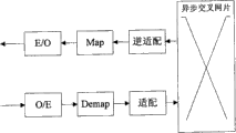
现有第二种技术方案,来自于专利号为US 2003/001616416的美国专利。参见图3所示,该系统主要由晶振单元、映射单元(Map)、解映射单元(Demap)、串/并单元、并/串单元以及同步交叉网片组成。The existing second technical solution comes from the US patent No. US 2003/001616416. Referring to Fig. 3, the system is mainly composed of a crystal oscillator unit, a mapping unit (Map), a demapping unit (Demap), a serial/parallel unit, a parallel/serial unit and a synchronous crossover network.
信号交叉调度过程中,输入的OTU3/OTU2/OTU1信号分别进入对应速率的Map单元21、24、27,进行一定数量字节的填塞映射后到达一个更高速率,完成信号的透明映射,此时各路信号的速率刚好为SDH基本速率单元STM-1(155.52Mbps)的整数倍,即OTU3->288×155.52Mbps=44.78976Gbps,OTU2->72×155.52Mbps=11.19744Gbps,OTU1->18×155.52Mbps=2.79936Gbps。这些填塞字节映射过程的作用是完成OTUk信号到SDH容器频差的平滑,是一种异步映射过程,以保证所有OTUk信号的同步。During the signal cross-scheduling process, the input OTU3/OTU2/OTU1 signals enter the
然后,从Map单元21、24、27输出的这些串行高速信号经过S/P单元22、25、28分别转换成64/16/4路并行信号,其单线速率为699.84Mbps,即S/P单元22、25、28分别完成44.78976Gbps->64×669.84Mbps,11.19744Gbps->16×669.84Mbps,2.79936Gbps->4×669.84Mbps的转换,以使调度系统在669.84MHz基准频率上进行同步调度,从而实现OTU3/2/1信号的调度功能。Then, these serial high-speed signals output from
并行信号进入基于699.84Mbps颗粒的同步交叉网片10进行交叉调度后,进入P/S单元32、35、38分别转换成串行高速信号,其单线速率为699.84Mbps,即P/S单元32、35、38分别完成64×669.84Mbps->44.78976Gbps,16×669.84Mbps->11.19744Gbps,4×669.84Mbps->2.79936Gbps的转换。After the parallel signal enters the synchronous
最后,串行高速信号进入Demap单元31、34、37,进行和Map过程相反的去填塞解映射过程,从高速串行信号中恢复出内部的OTU3/2/1业务数据输出。Finally, the serial high-speed signals enter the
其中,晶振单元15输出44.78976GHz的时钟信号fo,并且该时钟信号fo还进一步进入1/4分频单元16、1/16分频单元17和1/N分频单元18;时钟信号fo通过1/4分频单元161/16分频单元17的分频处理得到11.19744GHz和2.79936GHz的时钟信号fo/4和fo/16。这些输出的时钟信号可分别送给对应的Map/Demap单元用于OTU3/2/1业务与44.78976Gbps、11.19744Gbps、2.79936Gbps串行高速信号之间的异步映射/解映射。1/N分频单元18的分频比N为串/并(S/P)单元28并行位宽的16倍,即4×16=64,用于产生各S/P单元、背板调度系统、P/S单元的基准频率699.84MHz。Wherein,
现有技术二的缺点是:该技术是基于OTU1/OTU2/OTU3信号传送单元的调度,未实现ODU1/ODU2/ODU3的连接层次功能,这样对于OTN网络的连接监视管理无法实现,其不是一个完整的OTN设备单元,只是完成了OTU1/OTU2/OTU3的调度功能。OTU1/OTU2/OTU3的异步映射的填塞方法不尽相同,因此传送单元之间无法互通,只能构成独立的OTU1或OTU2或OTU3的OTN网络,使OTN网络组网受到限制。The disadvantage of
发明内容 Contents of the invention
有鉴于此,本发明的主要目的在于提供一种光传送网中实现信号调度的方法,实现高低各种速率级别信号的交叉调度,降低系统设计的复杂性,实现各速率级别信号之间的分插复用以及交叉连接功能,以提高OTN网络的组网灵活性。In view of this, the main purpose of the present invention is to provide a method for realizing signal scheduling in an optical transport network, realize cross-scheduling of high and low rate level signals, reduce the complexity of system design, and realize splitting between signals of various rate levels. Insert multiplexing and cross-connection functions to improve the networking flexibility of the OTN network.
基于上述目的本发明提供的一种光传送网络中的信号调度方法,包括:Based on the above purpose, the present invention provides a signal scheduling method in an optical transport network, including:
将所接收的光信号经光电转换处理成为电信号,再进行解映射处理后,将信号速率适配至一个统一的颗粒级别,在基于该颗粒级别的异步交叉矩阵中进行异步交叉调度处理;The received optical signal is converted into an electrical signal by photoelectric conversion, and then demapped, the signal rate is adapted to a uniform granular level, and asynchronous cross-connect scheduling processing is performed in the asynchronous cross-connect matrix based on the granular level;
所述信号速率适配的过程包括:The process of the signal rate adaptation includes:
对于当前信号的速率大于所述颗粒级别的情况,For the case where the rate of the current signal is greater than the granular level,
如果所接收信号是由多路速率为所述颗粒级别的低速信号映射复用而成的,则将当前信号时分解复用成多路所述的低速信号;If the received signal is formed by mapping and multiplexing the low-speed signal whose rate is the granular level, the current signal is time-decomposed and multiplexed into multiple low-speed signals;
如果所接收信号是由一路速率大于所述颗粒级别的高速信号映射而成的,则将当前信号拆分成多路速率为所述颗粒级别的并行信号;If the received signal is mapped from a high-speed signal with a rate greater than the granular level, split the current signal into multiple parallel signals with a rate equal to the granular level;
如果所接收信号是由一路以上速率大于所述颗粒级别的高速信号映射复用而成的,则将当前信号时分解复用成多路所述的高速信号,将得到的每路高速信号拆分成多路速率为所述颗粒级别的并行信号。If the received signal is formed by mapping and multiplexing of more than one high-speed signal whose rate is greater than the granular level, the current signal is time-decomposed and multiplexed into multiple high-speed signals described above, and each obtained high-speed signal is split into multiplexed parallel signals at the granular level.
该方法所述信号速率适配的过程包括:The process of signal rate adaptation described in the method includes:
经过解映射处理后,如果当前信号的速率等于所述颗粒级别,则将当前信号直接送入所述异步交叉矩阵进行异步交叉调度;After the demapping process, if the rate of the current signal is equal to the granular level, the current signal is directly sent to the asynchronous cross-connect matrix for asynchronous cross-connect scheduling;
如果当前信号的速率小于所述颗粒级别,则将多路与当前信号同种类型的信号合并成一路速率为所述颗粒级别的信号。If the rate of the current signal is lower than the granular level, multiple signals of the same type as the current signal are combined into one signal whose rate is the granular level.
该方法所述接收的光信号为ITU-T G.709协议下的光信号。The received optical signal described in the method is an optical signal under the ITU-T G.709 protocol.
该方法所述统一的颗粒级别为ODU1速率级别;The unified granular level described in the method is the ODU1 rate level;
如果所接收的光信号为由1路ODU1映射而成的OTU1,则所述信号速率适配的过程为将解映射后形成的ODU1进行ODU成帧、扰码处理后,送入所述异步交叉矩阵进行异步交叉调度;If the received optical signal is an OTU1 mapped from one ODU1, the process of signal rate adaptation is to perform ODU framing and scrambling on the ODU1 formed after demapping, and then send it to the asynchronous crossover The matrix performs asynchronous cross-scheduling;
如果所接收的光信号为由4路ODU1映射复用而成的OTU2,则所述信号速率适配的过程为将解映射后形成的ODU2时分解复用为4路ODU1后,进行ODU成帧、扰码处理;If the received optical signal is an OTU2 formed by mapping and multiplexing 4-way ODU1, the process of signal rate adaptation is to decompose and multiplex the ODU2 formed after demapping into 4-way ODU1, and then perform ODU framing , scrambling code processing;
如果所接收的光信号为由16路ODU1映射复用而成的OTU3,则所述信号速率适配的过程为将解映射后形成的ODU3时分解复用为16路ODU1,进行ODU成帧、扰码处理后;If the received optical signal is an OTU3 formed by mapping and multiplexing 16-way ODU1, the process of signal rate adaptation is to decompose and multiplex the ODU3 formed after demapping into 16-way ODU1, and perform ODU framing, After scrambling;
如果所接收的光信号为由1路ODU2映射而成的OTU2,则所述信号速率适配的过程为将解映射后形成的ODU2进行ODU成帧、扰码处理后,使用通道化成帧的方法拆分为4路速率为ODU1速率级别的并行信号;If the received optical signal is an OTU2 mapped from one ODU2, the signal rate adaptation process is to perform ODU framing and scrambling on the ODU2 formed after demapping, and then use channelization framing Split into 4 parallel signals whose rate is ODU1 rate level;
如果所接收的光信号为由1路ODU3映射而成的OTU3,则所述信号速率适配的过程为将解映射后形成的ODU3进行ODU成帧、扰码处理后,使用通道化成帧的方法拆分为16路速率为ODU1速率级别的并行信号;If the received optical signal is an OTU3 mapped from one ODU3, the signal rate adaptation process is to perform ODU framing and scrambling on the ODU3 formed after demapping, and then use channelization framing Split into 16 parallel signals whose rate is ODU1 rate level;
如果所接收的光信号为由4路ODU2映射复用而成的OTU3,则所述信号速率适配的过程为将解映射后形成的ODU3时分解复用为4路ODU2后,进行ODU成帧、扰码处理,将得到的每路ODU2分别使用通道化成帧的方法拆分为4路速率为ODU1速率级别的并行信号。If the received optical signal is an OTU3 formed by mapping and multiplexing 4-way ODU2, the process of signal rate adaptation is to decompose and multiplex the ODU3 formed after demapping into 4-way ODU2, and then perform
该方法所述解映射的处理过程包括:OTU定帧、解扰、FEC解码、OTU开销终结、ODU解映射。The demapping process described in the method includes: OTU framing, descrambling, FEC decoding, OTU overhead termination, and ODU demapping.
该方法所述拆分的过程为:对信号进行定帧处理后,按帧的顺序进行缓存,每当存满n帧后,将该n帧的数据并行发出,并重复执行上述拆分的过程;其中n为当前信号欲拆分成的路数。The splitting process described in this method is: after the signal is frame-fixed, it is buffered in the order of the frames, and whenever n frames are full, the data of the n frames are sent in parallel, and the above splitting process is repeated ; where n is the number of channels to split the current signal into.
该方法所述解映射的处理过程在执行完ODU解映射后进一步包括:ODU映射、OTU成帧、FEC编码增加FEC区域、扰码;所述统一的颗粒级别为OTU1速率级别;The process of demapping described in the method further includes after ODU demapping is performed: ODU mapping, OTU framing, FEC coding, adding FEC area, and scrambling; the unified granular level is OTU1 rate level;
如果所接收的光信号为由1路ODU1映射而成的OTU1,则所述信号速率适配的过程为将解映射处理过程后形成的ODU1信号进行ODU1映射、OTU1成帧、FEC编码、扰码处理后,形成OTU1,送入所述异步交叉矩阵进行异步交叉调度;If the received optical signal is an OTU1 mapped by one ODU1, the signal rate adaptation process is to perform ODU1 mapping, OTU1 framing, FEC encoding, and scrambling on the ODU1 signal formed after the demapping process After processing, OTU1 is formed and sent to the asynchronous cross-connect matrix for asynchronous cross-connect scheduling;
如果所接收的光信号为由4路ODU1映射复用而成的OTU2,则所述信号速率适配的过程为将解映射处理过程后形成的ODU2时分解复用为4路ODU1信号,进行ODU1映射、OTU1成帧、FEC编码、扰码处理后,形成4路OTU1,进入异步交叉调度;If the received optical signal is OTU2 formed by mapping and multiplexing 4-way ODU1, then the process of signal rate adaptation is to decompose and multiplex the ODU2 formed after the demapping process into 4-way ODU1 signal, and perform ODU1 After mapping, OTU1 framing, FEC encoding, and scrambling processing, 4 channels of OTU1 are formed and enter asynchronous cross-scheduling;
如果所接收的光信号为由16路ODU1映射复用而成的OTU3,则所述信号速率适配的过程为将解映射处理过程后形成的ODU3时分解复用为16路ODU1信号,进行ODU1映射、OTU1成帧、FEC编码、扰码处理后,形成16路OTU1,进入异步交叉调度;If the received optical signal is an OTU3 formed by mapping and multiplexing 16 ODU1 channels, the signal rate adaptation process is to decompose and multiplex the ODU3 formed after the demapping process into 16 ODU1 signals, and perform ODU1 After mapping, OTU1 framing, FEC encoding, and scrambling processing, 16 channels of OTU1 are formed and enter asynchronous cross-scheduling;
如果所接收的光信号为由1路ODU2映射而成的OTU2,则所述信号速率适配的过程为将解映射处理过程后形成的ODU2进行ODU2映射、OTU2成帧、FEC编码、扰码处理后,形成OTU2,使用通道化成帧的方法拆分为4路速率为OTU1速率级别的并行信号,进入异步交叉调度;If the received optical signal is an OTU2 mapped from one ODU2, the signal rate adaptation process is to perform ODU2 mapping, OTU2 framing, FEC encoding, and scrambling processing on the ODU2 formed after the demapping process After that, OTU2 is formed, which is split into 4 parallel signals whose rate is OTU1 rate level by channelized framing method, and enters asynchronous cross-scheduling;
如果所接收的光信号为由1路ODU3映射而成的OTU3,则所述信号速率适配的过程为将解映射处理过程后形成的ODU3进行ODU3映射、OTU3成帧、FEC编码、扰码处理后,形成OTU3,使用通道化成帧的方法拆分为16路速率为OTU1速率级别的并行信号,进入异步交叉调度;If the received optical signal is an OTU3 mapped by one ODU3, the signal rate adaptation process is to perform ODU3 mapping, OTU3 framing, FEC encoding, and scrambling processing on the ODU3 formed after the demapping process After that, OTU3 is formed, which is split into 16 parallel signals whose rate is OTU1 rate level by channelized framing method, and enters asynchronous cross-scheduling;
如果所接收的光信号为由4路ODU2映射复用而成的OTU3,则所述信号速率适配的过程为将解映射处理过程后形成的ODU3时分解复用为4路ODU2信号,进行ODU2映射、OTU2成帧、FEC编码、扰码处理后,形成4路OTU2,将得到的每路OTU2分别使用通道化成帧的方法拆分为4路速率为OTU1速率级别的并行信号,进入异步交叉调度。If the received optical signal is an OTU3 formed by mapping and multiplexing 4-way ODU2, the process of signal rate adaptation is to decompose and multiplex the ODU3 formed after the de-mapping process into 4-way ODU2 signals, and perform ODU2 After mapping, OTU2 framing, FEC encoding, and scrambling processing, 4 channels of OTU2 are formed, and each channelized OTU2 is split into 4 channels of parallel signals with a rate of OTU1 rate level, and enters asynchronous cross-scheduling .
该方法所述拆分过程为:对信号按帧的顺序进行缓存,每当存满n帧后,将该n帧的数据并行发出,并重复执行上述拆分的过程;其中n为当前信号的欲拆分成的路数。The splitting process described in this method is: buffer the signal in the order of frames, and send out the data of the n frames in parallel every time n frames are stored, and repeat the above splitting process; where n is the number of current signals The number of paths to split into.
该方法其特征在于,所述异步交叉调度处理后,进一步包括:执行所述信号速率适配的过程的逆过程,进行解映射处理和电光转换成为光信号后输出。The method is characterized in that, after the asynchronous cross-connect scheduling processing, it further includes: performing a reverse process of the signal rate adaptation process, performing demapping processing and electro-optical conversion into an optical signal and then outputting it.
本发明的另一主要目的是一种光传送网中实现信号调度的系统,可支持高低各种速率级别信号的交叉调度,降低系统设计的复杂性,支持各速率级别信号之间的分插复用以及交叉连接功能,提高OTN网络的组网灵活性。Another main purpose of the present invention is a system for implementing signal scheduling in an optical transport network, which can support cross-scheduling of signals of various rate levels, reduce the complexity of system design, and support add-drop multiplexing between signals of various rate levels. Use and cross-connection functions to improve the networking flexibility of the OTN network.
基于该目的本发明提供的一种光传送网络中的信号调度系统,包括:Based on this purpose, the present invention provides a signal scheduling system in an optical transmission network, including:
至少一个光电转换单元,用于将接收的光信号转换为电信号;at least one photoelectric conversion unit for converting received optical signals into electrical signals;
至少一个解映射单元,用于对信号进行解映射处理;at least one demapping unit, configured to demap signals;
至少一个适配装置,用于将输入信号适配为统一的颗粒级别的信号;以及at least one adapting device for adapting the input signal to a uniform granular level signal; and
异步交叉矩阵,用于对统一颗粒级别的信号进行异步交叉调度;Asynchronous cross matrix, used for asynchronous cross scheduling of signals at a uniform granularity level;
接收的光信号经光电转换单元转换为电信号后,输入至解映射单元,经解映射处理输出后,进入适配装置,适配成速率符合所述统一的颗粒级别的信号后输入至异步交叉矩阵进行异步交叉调度;After the received optical signal is converted into an electrical signal by the photoelectric conversion unit, it is input to the demapping unit, and after being processed and output by demapping, it enters the adaptation device, and is adapted into a signal whose rate conforms to the unified granular level, and then input to the asynchronous crossover The matrix performs asynchronous cross-scheduling;
如果所述输入信号是由多路速率为所述颗粒级别的低速信号映射复用而成的,所述适配装置中包括:信号生成单元和时分解复用单元,时分解复用单元用于将由多路低速信号映射复用而成的高速信号时分解复用为多路速率为所述统一颗粒级别的低速信号,并输出至所述信号生成单元;If the input signal is formed by mapping and multiplexing the low-speed signal whose multi-channel rate is the granular level, the adaptation device includes: a signal generation unit and a time division multiplexing unit, and the time division multiplexing unit is used for Time-decomposing and multiplexing the high-speed signal formed by mapping and multiplexing multiple low-speed signals into multiple low-speed signals whose rate is the same granular level, and outputting to the signal generation unit;
如果所接收信号是由一路速率大于所述颗粒级别的高速信号映射而成的,所述适配装置中包括:信号生成单元和拆分单元,拆分单元用于将所述信号生成单元处理后输出的信号拆分为多路速率为所述统一颗粒级别的并行信号;If the received signal is mapped from a high-speed signal with a rate greater than the granular level, the adaptation device includes: a signal generating unit and a splitting unit, and the splitting unit is used to process the signal generating unit The output signal is split into multiple parallel signals whose rate is the unified granularity level;
如果所接收信号是由一路以上速率大于所述颗粒级别的高速信号映射复用而成的,所述适配装置中包括:信号生成单元、时分解复用单元和拆分单元,时分解复用单元将由多路低速信号映射复用而成的高速信号解复用为多路所述低速信号输入至所述信号生成单元和拆分单元,拆分单元将信号生成单元处理后输出的低速信号进一步拆分为所述统一颗粒级别的并行信号。If the received signal is formed by mapping and multiplexing of more than one high-speed signal whose rate is greater than the granular level, the adaptation device includes: a signal generation unit, a time division multiplexing unit and a splitting unit, and a time division multiplexing unit The unit demultiplexes the high-speed signal formed by mapping and multiplexing multiple low-speed signals into multiple low-speed signals and inputs them to the signal generating unit and the splitting unit, and the splitting unit further processes the low-speed signal outputted by the signal generating unit Split into parallel signals at the uniform granularity level.
如果所述输入信号的速率为所述统一颗粒级别,所述适配装置为用于信号成帧、扰码的信号生成单元。If the rate of the input signal is at the uniform granularity level, the adapting device is a signal generating unit for signal framing and scrambling.
该系统所述拆分单元包括:定帧模块、写地址产生模块、读地址产生模块、n分频模块、以及2n个先入先出存储器FIFO,其中,n为信号经该拆分单元拆分后输出的信号路数;The splitting unit of the system includes: a framing module, a write address generation module, a read address generation module, an n frequency division module, and 2n first-in-first-out memory FIFOs, where n is the signal split by the splitting unit The number of output signal channels;
输入信号具有随路同步时钟,经定帧模块的搜帧处理后得到帧信号,同步时钟与帧信号一起输入写地址产生模块,产生写地址和写允许分别进入每个先入先出存储器FIFO,控制先入先出存储器FIFO的写入,同时信号时钟还输入至n分频模块,经n分频模块分频后的输出与帧信号一起输入至读地址产生模块,产生读地址和读允许分别进入每个先入先出存储器FIFO,控制先入先出存储器FIFO的读出;The input signal has a synchronous clock along with the channel, and the frame signal is obtained after the frame search process of the framing module. The synchronous clock and the frame signal are input to the write address generation module together, and the generated write address and write permission enter each first-in-first-out memory FIFO respectively, and control The first-in-first-out memory FIFO is written, and the signal clock is also input to the n frequency division module. The output after frequency division by the n frequency division module is input to the read address generation module together with the frame signal, and the read address and read permission are respectively entered into each A first-in-first-out memory FIFO, which controls the readout of the first-in-first-out memory FIFO;
输入信号的数据按帧的顺序依次写入n个先入先出存储器FIFO,写满后n个先入先出存储器FIFO中的数据并行输出,同时后面的数据依次写入另外的n个先入先出存储器FIFO,写满后所述另外n个先入先出存储器FIFO中的数据并行输出。The data of the input signal is sequentially written into n first-in-first-out memory FIFOs in the order of frames, and the data in the n first-in-first-out memory FIFOs are output in parallel after being filled, and the subsequent data are sequentially written into another n first-in first-out memory After the FIFO is full, the data in the other n first-in-first-out memory FIFOs are output in parallel.
该系统进一步包括:至少一个电光转换单元,用于将接收的电信号转换为光信号;The system further includes: at least one electro-optical conversion unit for converting the received electrical signal into an optical signal;
至少一个映射单元,用于对信号进行映射处理;At least one mapping unit, configured to perform mapping processing on signals;
至少一个逆适配装置,用于将所述异步交叉矩阵输出的统一的颗粒级别的信号反向适配为所需速率的信号;at least one inverse adaptation device, configured to inversely adapt the uniform granular level signal output by the asynchronous crossbar matrix to a signal of a required rate;
异步交叉矩阵进行异步交叉调度后输出的信号,进入逆适配装置进行反向适配处理,输入至映射单元,经映射处理后,进入电光转换单元转换为光信号。The signal output by the asynchronous cross-connect matrix after asynchronous cross-connect scheduling enters the inverse adaptation device for reverse adaptation processing, and is input to the mapping unit. After mapping processing, it enters the electro-optical conversion unit to be converted into an optical signal.
该系统如果所需输出信号的速率为所述统一颗粒级别,所述逆适配装置包括:定帧对齐单元和信号恢复单元,所述定帧对齐单元对异步交叉矩阵输出的统一颗粒级别的信号进行定帧对齐处理后输入至信号恢复单元进行解扰码处理后输出;If the rate of the required output signal of the system is the uniform granularity level, the inverse adaptation device includes: a frame alignment unit and a signal recovery unit, and the frame alignment unit outputs the uniform granularity level signal output by the asynchronous cross matrix After performing frame alignment processing, input to the signal recovery unit for descrambling processing and then output;
如果所需输出的为由多路速率为所述颗粒级别的低速信号映射复用而成的信号,所述逆适配装置包括:定帧对齐单元、信号恢复单元和时分复用单元,时分复用单元用于将经所述定帧对齐单元和信号恢复单元输出的多路低速信号时分复用为一路所需速率级别的高速信号后输出;If the required output is a signal formed by mapping and multiplexing the low-speed signal at the granular level, the inverse adaptation device includes: a frame alignment unit, a signal recovery unit and a time division multiplexing unit, and the time division multiplexing The use unit is used to time-multiplex the multiple low-speed signals output by the frame alignment unit and the signal recovery unit into one high-speed signal of the required rate level and then output it;
如果所需输出的为由一路速率大于所述颗粒级别的高速信号映射而成的信号,所述逆适配装置包括:定帧对齐单元、信号恢复单元和合并单元,所述定帧对齐单元将所述异步交叉矩阵输出的每组统一颗粒级别的并行信号进行定帧对齐处理后输入至合并单元,合并单元将多路并行信号合并为一路所需速率级别的高速信号后输入至信号恢复单元解扰码处理后输出;If the required output is a signal mapped by a high-speed signal with a rate greater than the granular level, the inverse adaptation device includes: a frame alignment unit, a signal recovery unit and a merging unit, and the frame alignment unit will Each set of parallel signals at the same granularity level output by the asynchronous cross matrix is processed by frame alignment and then input to the merging unit, which merges multiple parallel signals into one high-speed signal of the required rate level and then inputs it to the signal recovery unit for solution. output after scrambling;
如果所需输出的为由一路以上速率大于所述颗粒级别的高速信号映射复用而成的信号,所述逆适配装置包括:定帧对齐单元、信号恢复单元、时分复用单元和合并单元,所述定帧对齐单元将所述异步交叉矩阵输出的每组统一颗粒级别的并行信号进行定帧对齐处理后输入至合并单元,合并单元将多路并行信号合并为一路信号后输入至信号恢复单元解扰码处理后输出至时分复用单元时分复用为一路所需速率级别的高速信号后输出。If the desired output is a signal formed by mapping and multiplexing more than one high-speed signal whose rate is greater than the granular level, the inverse adaptation device includes: a frame alignment unit, a signal recovery unit, a time division multiplexing unit and a merging unit , the frame-alignment unit performs frame-alignment processing on each group of parallel signals at a uniform granularity level output by the asynchronous cross matrix and then inputs them to the merging unit, and the merging unit merges multiple parallel signals into one signal and then inputs it to the signal recovery The unit descrambles and outputs to the time division multiplexing unit after time division multiplexing into one high-speed signal of the required rate level and then outputs.
该系统所述合并单元,内部设置有2n个先入先出存储器FIFO,每个先入先出存储器FIFO存储一帧数据,数据和参考帧信号依次写入n个先入先出存储器FIFO进行对齐处理,与此同时,以n倍于写操作的速率依次从另外n个先入先出存储器FIFO中读取数据并输出;其中,n为信号经该拆分单元拆分后输出的信号路数;The merging unit of the system is internally provided with 2n first-in-first-out memory FIFOs, and each first-in-first-out memory FIFO stores a frame of data, and data and reference frame signals are sequentially written into n first-in-first-out memory FIFOs for alignment processing, and At the same time, the data is sequentially read and output from other n first-in-first-out memory FIFOs at a rate n times higher than that of the write operation; wherein, n is the number of signal paths output after the signal is split by the splitting unit;
所述定帧对齐单元包括:The frame alignment unit includes:
背板接口模块,用于对输入的n路信号进行时钟数据恢复,将恢复后的n路时钟和数据信号输入至定帧对齐模块,选择其中一路时钟作为参考时钟分别发送至定帧对齐模块和所述合并单元;The backplane interface module is used to restore the clock and data of the input n-channel signals, input the recovered n-channel clock and data signals to the frame alignment module, and select one of the clocks as a reference clock and send them to the frame alignment module and the frame alignment module respectively. said merging unit;
定帧对齐模块,用于对每路信号分别进行帧搜索,找到n路信号各自的帧起始位置,将n路信号的帧起始位置都对齐到相同的帧相位上,输出n路对齐的数据和参考帧信号至所述合并单元。The fixed frame alignment module is used to perform frame search on each channel of signals, find the respective frame starting positions of n channels of signals, align the frame starting positions of n channels of signals to the same frame phase, and output the n channels of aligned data and reference frame signals to the merging unit.
该系统所述异步交叉矩阵为异步交叉网片。The asynchronous cross-connect matrix in the system is an asynchronous cross-connect mesh.
从上面所述可以看出,本发明提供的一种光传送网中信号调度的方法和系统具有如下特点和优点:It can be seen from the above that the method and system for signal scheduling in an optical transport network provided by the present invention have the following characteristics and advantages:
1)采用信号速率适配的方式,使无论哪种速率级别的信号都可以到转换为统一速率级别,并在统一异步交叉矩阵中进行调度,而无需多级交叉单元,从而降低了系统设计的复杂性,并且统一调度能够实现各速率级别信号之间的灵活分插复用,提高了OTN网络的组网灵活性。1) The signal rate adaptation method is adopted, so that signals of any rate level can be converted to a uniform rate level and scheduled in a unified asynchronous cross-connect matrix without the need for multi-level cross-connect units, thereby reducing the cost of system design Complexity, and unified scheduling can realize flexible add-drop multiplexing between signals of various rate levels, which improves the networking flexibility of the OTN network.
2)本发明拓展了现有技术信号的时分复用/解复用技术,将高速信号拆分成多路低速并行信号捆绑调度,通过通道化成帧的并行信号上传送高速信号颗粒,并且在调度系统中使用相同的调度路径,从而实现高速信号颗粒的调度功能。使在现有异步交叉芯片技术水平上,解决了ODU2/ODU3更高速率信号的调度问题。2) The present invention expands the time-division multiplexing/demultiplexing technology of signals in the prior art, splits high-speed signals into multiple low-speed parallel signals for bundling and scheduling, and transmits high-speed signal particles on the parallel signals channelized into frames, and in scheduling The same scheduling path is used in the system to realize the scheduling function of high-speed signal particles. On the level of the existing asynchronous cross-chip technology, the scheduling problem of ODU2/ODU3 higher rate signals is solved.
附图说明 Description of drawings
图1为ITU-T G.709定义的各种信号之间的映射复用路径示意图;Figure 1 is a schematic diagram of the mapping and multiplexing paths between various signals defined by ITU-T G.709;
图2为现有第一种技术方案的信号调度系统结构示意图;Fig. 2 is the structural diagram of the signal dispatching system of the existing first technical solution;
图3为现有第二种技术方案的信号调度系统结构示意图;Fig. 3 is the structural diagram of the signal dispatching system of the second existing technical solution;
图4为本发明信号调度系统的结构框图;Fig. 4 is the structural block diagram of the signal dispatching system of the present invention;
图5为本发明信号调度系统中适配装置的结构示意图;FIG. 5 is a schematic structural diagram of an adaptation device in the signal dispatching system of the present invention;
图6为本发明信号调度系统中逆适配装置的结构示意图;6 is a schematic structural diagram of an inverse adaptation device in the signal dispatching system of the present invention;
图7为本发明可同时对基于ODU1/ODU2/ODU3进行统一调度的系统结构示意图;FIG. 7 is a schematic structural diagram of a system that can simultaneously perform unified scheduling based on ODU1/ODU2/ODU3 according to the present invention;
图8为ITU-T G.709规定的从ODUk到OTUk的映射结构示意图;Figure 8 is a schematic diagram of the mapping structure from ODUk to OTUk specified in ITU-T G.709;
图9为本发明信号调度系统中的ODU2拆分单元的结构示意图;9 is a schematic structural diagram of the ODU2 splitting unit in the signal dispatching system of the present invention;
图10为本发明信号调度系统中针对ODU2信号的ODU2FIFO合并单元的结构示意图;10 is a schematic structural diagram of an ODU2FIFO merging unit for ODU2 signals in the signal dispatching system of the present invention;
图11为本发明针对ODU2信号的ODU2FIFO合并单元中背板接口模块的结构示意图;Fig. 11 is a schematic structural diagram of the backplane interface module in the ODU2FIFO merging unit of the present invention for ODU2 signals;
图12为本发明针对ODU2信号的ODU2FIFO合并单元中定帧对齐模块的结构示意图;FIG. 12 is a schematic structural diagram of the frame alignment module in the ODU2FIFO merging unit for ODU2 signals in the present invention;
图13为本发明定帧对齐模块帧对齐过程的时序图;FIG. 13 is a timing diagram of the frame alignment process of the frame alignment module of the present invention;
图14为本发明本发明针对ODU2信号的ODU2FIFO合并单元中ODU2FIFO合并单元的结构示意图。FIG. 14 is a schematic structural diagram of the ODU2FIFO merging unit in the ODU2FIFO merging unit for ODU2 signals in the present invention.
具体实施方式 Detailed ways
下面结合附图及具体实施例对本发明再作进一步详细的说明。The present invention will be further described in detail below in conjunction with the accompanying drawings and specific embodiments.
本发明的核心思路为:在现有高速异步交叉技术的基础上,为了统一ODU1/ODU2/ODU3信号的调度单元,将所接收的光信号经光电转换成为电信号,并进行解映射处理后,适配至一个统一的颗粒级别,在基于该颗粒级别的同一个异步交叉矩阵中进行异步交叉调度处理。The core idea of the present invention is: on the basis of the existing high-speed asynchronous crossover technology, in order to unify the scheduling unit of the ODU1/ODU2/ODU3 signal, the received optical signal is converted into an electrical signal through photoelectricity, and after demapping processing, Adapt to a unified granular level, and perform asynchronous cross-connect scheduling processing in the same asynchronous cross-connect matrix based on the granular level.
进行适配过程中,如果信号的速率大于所述统一的颗粒级别,则将当前信号分解成多路信号,使每路信号的速率满足所述统一的颗粒级别;如果信号的速率等于所述统一的颗粒级别,则信号经解映射后可直接送入异步交叉矩阵进行异步交叉调度;如果信号的速率小于所述统一的颗粒级别,则可将多路信号通过时分复用等方式合并成一路信号,使该信号的速率满足所述颗粒级别。During the adaptation process, if the rate of the signal is greater than the unified granular level, the current signal is decomposed into multiple signals so that the rate of each signal meets the unified granular level; if the signal rate is equal to the unified granular level At the granular level, the signal can be directly sent to the asynchronous cross-connect matrix for asynchronous cross-connect scheduling after demapping; if the signal rate is lower than the unified granular level, multiple signals can be combined into one signal by means of time division multiplexing, etc. , so that the rate of the signal satisfies the grain level.
这其中,当信号的速率大于所述统一的颗粒级别时,又有三种情况,以ITU-T G.709协议下,采用基于2.5Gbps颗粒级别的异步交叉矩阵为例:Among them, when the signal rate is greater than the unified granular level, there are three situations. Take the asynchronous cross matrix based on the 2.5Gbps granular level under the ITU-T G.709 protocol as an example:
第一种情况,该信号是由多路速率为所述颗粒级别的低速信号映射复用而成的,比如:当前的OTU2或OTU3是由4路或16路ODU1映射复用而成的,则只需将当前信号进行时分解复用,还原成多路速率为所述颗粒级别的低速信号,即将OTU2经解映射后的ODU2信号时分解复用为4路ODU1,将OTU3经解映射后的ODU3信号时分解复用为16路ODU1。In the first case, the signal is formed by mapping and multiplexing the low-speed signal at the granular level. For example, the current OTU2 or OTU3 is formed by mapping and
第二种情况,该信号是由一路速率大于所述颗粒级别的高速信号映射而成的,比如:当前的OTU2是由ODU2映射而成的,或OTU3是由ODU3映射而成的,则应将当前信号拆分成多路速率为所述颗粒级别的并行信号,比如:将OTU2经解映射为ODU2后,再使用通道化成帧的方法拆分成4路速率级别为2.5Gbps的信号,即ODU1速率级别,再并行发送至异步交叉矩阵,并且在调度时使用相同的调度路径,使并行信号捆绑调度,由于这4路信号组合在一起才能构成完整的ODU2,因此为描述方便,本发明将拆分后的ODU2表示为ODU2[3:0],每个ODU2[3:0]中包含有4个ODU1速率级别的信号;将OTU3经解映射为ODU3后,再使用通道化成帧的方法拆分成16路ODU1速率级别的信号,再并行发送至异步交叉矩阵绑定调度,为描述方便,本发明将拆分后的ODU3表示为ODU3[15:0],每个ODU3[15:0]中包含有16个ODU1速率级别的信号。In the second case, the signal is mapped from a high-speed signal with a rate greater than the granular level, for example: the current OTU2 is mapped from ODU2, or OTU3 is mapped from ODU3, then the The current signal is split into multiple parallel signals whose rate is at the granular level. For example, after OTU2 is demapped into ODU2, it is split into 4 signals with a rate of 2.5Gbps, that is, ODU1, using the method of channelization and framing. The rate level is sent to the asynchronous cross matrix in parallel, and the same scheduling path is used during scheduling, so that the parallel signals are bundled and scheduled. Since these 4 signals can be combined to form a complete ODU2, so for the convenience of description, the present invention will disassemble The divided ODU2 is represented as ODU2[3:0], and each ODU2[3:0] contains 4 ODU1 rate level signals; after demapping OTU3 into ODU3, it is split by channelization and
第三种情况,该信号是由多路速率大于所述颗粒级别的高速信号映射复用而成的,比如:当前的OTU3是由4路ODU2映射复用而成的,则应将当前信号时分解复用成多路速率大于所述颗粒级别的高速信号,再将得到的每路高速信号拆分成多路速率为所述颗粒级别的并行信号,即OTU3经解映射为ODU3后,先解复用为4路ODU2,再将每路ODU2拆分为4路ODU1速率级别的信号,即ODU2[3:0],从而得到总共包含有16路ODU1速率级别的信号,即4×ODU2[3:0],并行发送至异步交叉矩阵。In the third case, the signal is multiplexed by multiplexed high-speed signals with a multi-channel rate greater than the granular level. For example, the current OTU3 is multiplexed by four-channel ODU2. Decompose and multiplex into multiple high-speed signals with a rate greater than the granular level, and then split each obtained high-speed signal into multiple parallel signals with a rate equal to the granular level, that is, after OTU3 is demapped into ODU3, the Multiplexing into 4 channels of ODU2, and then splitting each channel of ODU2 into 4 channels of ODU1 rate level signals, that is, ODU2[3:0], so as to obtain a total of 16 channels of ODU1 rate level signals, that is, 4×ODU2[3 :0], sent to the asynchronous crossbar matrix in parallel.
为实现上述方法本发明提供了一种信号调度系统,该系统的结构框图参见图4所示,至少应包括:用于对统一颗粒级别的信号进行异步交叉调度的异步交叉矩阵,以及至少一个光电转换单元、解映射单元和适配装置,用于对信号进行调度前的速率适配。调度过程为:所需要进行调度处理的光信号被该信号调度系统接收后,经光电转换单元转换为电信号后,输入至解映射单元,经解映射处理输出后,进入适配装置适配处理后,以统一的颗粒级别输出,进入异步交叉矩阵进行异步交叉调度。In order to realize the above method, the present invention provides a signal scheduling system. The structural block diagram of the system is shown in FIG. The conversion unit, the demapping unit and the adaptation device are used for performing rate adaptation on signals before scheduling. The dispatching process is as follows: after the optical signal required for dispatching processing is received by the signal dispatching system, it is converted into an electrical signal by the photoelectric conversion unit, and then input to the demapping unit. After being output by demapping processing, it enters the adaptation device for adaptation processing Finally, output at a unified granular level and enter the asynchronous cross-connect matrix for asynchronous cross-connect scheduling.
调度后输出的信号根据需要还可以再进一步进行反向适配,转换成传输所需速率的信号,这样在异步交叉矩阵的输出端还可在增加逆适配装置、映射单元和电光转换单元。这样,经异步交叉矩阵调度后的输出信号进入逆适配模块执行适配过从的逆过程,转换为所需速率的信号,经映射单元重新映射后,进入电光转换单元恢复为光信号后输出。The output signal after scheduling can be further reverse-adapted according to the need, and converted into a signal of the required rate for transmission, so that a reverse adaptation device, a mapping unit and an electro-optical conversion unit can also be added to the output of the asynchronous cross matrix. In this way, the output signal scheduled by the asynchronous cross matrix enters the inverse adaptation module to perform the inverse process of adaptation, and converts it into a signal of the required rate. After being remapped by the mapping unit, it enters the electro-optical conversion unit to restore to an optical signal and then outputs .
基于当前ITU-T G.709协议规定的各种连接信号ODU1/ODU2/ODU3,本发明适配装置的结构参见图5所示。Based on the various connection signals ODU1/ODU2/ODU3 specified in the current ITU-T G.709 protocol, the structure of the adaptation device of the present invention is shown in Figure 5.
对于ODU1信号,由于本实施例的异步交叉矩阵统一采用ODU1速率级别的,因此根据所需的不同输出信号对ODU1信号进行简单的成帧、适配等操作即可。具体来讲,如果需要输出ODU1信号,则ODU1的适配装置为用于扩展ODU帧头和信号扰码的ODU1信号生成单元501;如果需要在信号上增加控制信息比特和FEC纠错功能,输出带有FEC编码的OTU1信号,则ODU1的适配装置为用于ODU1映射、OTU1成帧、FEC编码以及扰码的OTU1信号生成单元502。For the ODU1 signal, since the asynchronous cross-connect matrix in this embodiment uniformly adopts the ODU1 rate level, it is sufficient to perform simple operations such as framing and adaptation on the ODU1 signal according to different output signals required. Specifically, if the ODU1 signal needs to be output, the ODU1 adaptation device is the ODU1
对于由4×ODU1复用而成的ODU2信号,如果需要输出带有FEC编码的4×OTU1信号,则ODU2的适配装置按信号流向依次包括:用于完成ODU2信号向4路低级别的ODU1信号时分解复用转换的时分解复用单元511,以及处理该多路信号的完成ODU1映射、OTU1成帧、FEC编码及扰码的OTU1信号生成单元502;如果需要输出4×ODU1信号,则ODU2的适配装置按信号流向依次包括:用于完成ODU2信号向4路低级别的ODU1信号时分解复用转换的时分解复用单元511,以及处理该多路信号的用于扩展ODU帧头和信号扰码的ODU1信号生成单元501。其中,由于需要经时分解复用单元511处理后输出的信号为4路,因此这里所述ODU1信号生成单元501、OTU1信号生成单元502应分别为4个(图5中为简化起见只绘出一个)。For the ODU2 signal multiplexed by 4×ODU1, if it is necessary to output the 4×OTU1 signal with FEC encoding, the adapter device of ODU2 includes in sequence according to the signal flow: used to complete the ODU2 signal to 4 low-level ODU1 Time-division-multiplexing
对于不是由低级信号复用而成的ODU2信号,如果需要输出带有FEC编码的OTU信号,则ODU2的适配装置按信号流向依次包括:完成ODU2映射、OTU2成帧、FEC编码及扰码的OTU2信号生成单元504,以及用于完成串行OTU2信号向OTU2[3:0]并行信号转换的OTU2拆分单元506;如果需要输出ODU2信号,则ODU2的适配装置按信号流向依次包括:用于扩展ODU帧头和信号扰码的ODU2信号生成单元503,以及用于完成串行ODU2信号向ODU2[3:0]并行信号转换的ODU2拆分单元505。For ODU2 signals that are not multiplexed by low-level signals, if it is necessary to output OTU signals with FEC encoding, the ODU2 adaptation device includes: ODU2 mapping, OTU2 framing, FEC encoding and scrambling according to the signal flow direction The OTU2
对于由16×ODU1复用而成的ODU3信号,如果需要输出带有FEC编码的16×OTU1信号,则ODU3的适配装置按信号流向依次包括:用于完成ODU3信号向16路低级别的ODU1信号时分解复用转换的时分解复用单元512,以及对应的16个OTU1信号生成单元502;如果需要输出16×ODU1信号,则ODU3的适配装置按信号流向依次包括:用于完成ODU3信号向多路低级别的ODU1信号时分解复用转换的时分解复用单元512,以及对应的16个ODU1信号生成单元501。For the ODU3 signal multiplexed by 16×ODU1, if it is necessary to output the 16×OTU1 signal with FEC encoding, the adapter device of ODU3 includes in order of signal flow: used to complete the ODU3 signal to 16 low-level ODU1 The time-division-multiplexing
对于由4×ODU2复用而成的ODU3信号,如果需要输出带有FEC编码的OTU信号,则ODU3的适配装置按信号流向依次包括:用于完成ODU3信号向4路低级别的ODU2信号时分解复用转换的时分解复用单元513,对应的4个OTU2信号生成单元504,以及对应的多个用于完成串行OTU2信号向OTU2[3:0]并行信号转换的OTU2拆分单元506;如果需要输出ODU信号,则ODU3的适配装置按信号流向依次包括:用于完成ODU3信号向4路低级别的ODU2信号时分解复用转换的时分解复用单元513,对应的4个ODU2信号生成单元503,以及对应的4个用于完成串行ODU2信号向ODU2[3:0]并行信号转换的ODU2拆分单元505。For the ODU3 signal multiplexed by 4×ODU2, if it is necessary to output the OTU signal with FEC encoding, the ODU3 adapter device includes in sequence according to the signal flow: for completing the ODU3 signal to 4 low-level ODU2 signals Demultiplexing
对于不是由低级信号复用而成的ODU3信号,如果需要输出带有FEC编码的OTU信号,则ODU3的适配装置按信号流向依次包括:用于完成ODU3映射、OTU3成帧、FEC编码及扰码的OTU3信号生成单元508,以及用于完成串行OTU3信号向OTU3[15:0]并行信号转换的OTU3拆分单元510;如果需要输出ODU信号,则ODU3的适配装置按信号流向依次包括:用于扩展ODU帧头和信号扰码的ODU3信号生成单元507,以及用于完成串行ODU3信号向ODU3[15:0]并行信号转换的ODU3拆分单元509。For ODU3 signals that are not multiplexed by low-level signals, if it is necessary to output OTU signals with FEC encoding, the ODU3 adaptation device includes in sequence according to the signal flow: for completing ODU3 mapping, OTU3 framing, FEC encoding and scrambling The OTU3
其中,上述ODUk/OTUk(k=1,2,3)信号生成单元在本发明中有时也统一称为信号生成单元,所述ODUk/OTUk(k=1,2,3)拆分单元也统一称为拆分单元。Wherein, the above-mentioned ODUk/OTUk (k=1, 2, 3) signal generation unit is sometimes collectively referred to as a signal generation unit in the present invention, and the ODUk/OTUk (k=1, 2, 3) splitting unit is also unified called a split unit.
基于当前ITU-T G.709协议规定的各种连接信号ODU1/ODU2/ODU3,本发明逆适配装置的结构参见图6所示。Based on the various connection signals ODU1/ODU2/ODU3 specified in the current ITU-T G.709 protocol, the structure of the reverse adaptation device of the present invention is shown in Figure 6.
对于需要逆适配为ODU1的信号,由于本实施例的异步交叉矩阵统一采用ODU1速率级别的,因此逆适配过程中,只需进行简单的定帧对齐,解扰码等处理。具体来讲,如果输入的为OTU1信号,则ODU1的逆适配装置为用于OTU1信号定帧对齐OTU1定帧对齐单元616,和完成解扰、FEC解码、ODU1解映射形成ODU1输出的OTU1信号恢复单元602;如果输入的为ODU1信号,则ODU1的逆适配装置为用于ODU1信号定帧对齐的ODU1定帧对齐单元615,和用于解扰的ODU1信号恢复单元601。For the signal that needs to be de-adapted to ODU1, since the asynchronous cross-connect matrix in this embodiment uniformly adopts the rate level of ODU1, during the de-adaptation process, only simple processing such as frame alignment and descrambling is required. Specifically, if the input is an OTU1 signal, the inverse adaptation device of ODU1 is the OTU1
对于需要逆适配为ODU2的信号,如果输入的为4×OTU1信号,则ODU2的逆适配装置按信号流向依次包括:OTU1定帧对齐单元616和4个具有解扰、FEC解码及ODU1解映射功能的OTU1信号恢复单元602,以及用于完成4路低级别的ODU1信号向ODU2信号时分复用转换的时分复用单元617;如果输入的为4×ODU1信号,则ODU2的逆适配装置按信号流向依次包括:ODU1定帧对齐单元615以及ODU1解扰功能的ODU1信号恢复单元601,以及用于完成多路低级别的ODU1信号向ODU2信号时分复用转换的时分复用单元617。For the signal that needs to be inversely adapted to ODU2, if the input is a 4×OTU1 signal, the inverse adaptation device of ODU2 includes in sequence according to the signal flow: OTU1
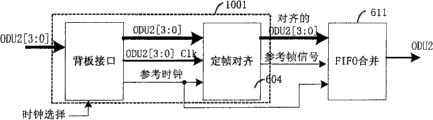
如果输入的为OTU2[3:0]信号,则ODU2的逆适配装置按信号流向依次包括:4个用于OTU2[3:0]定帧对齐的OTU2[3:0]定帧对齐单元604,用于完成OTU2[3:0]并行信号向串行OTU2信号转换的OTU2FIFO合并单元612,以及用于完成OTU2解扰、FEC解码和ODU2解映射功能形成ODU2的OTU2信号恢复单元606;如果输入的为ODU2[3:0]信号,则ODU2的逆适配装置按信号流向依次包括:4个用于ODU2[3:0]定帧对齐的ODU2[3:0]定帧对齐单元603,用于完成ODU2[3:0]并行信号向串行ODU2信号转换的ODU2FIFO合并单元611,以及完成ODU2解扰功能的ODU2信号恢复单元605。If the input is an OTU2[3:0] signal, the inverse adaptation device of ODU2 includes in sequence according to the signal flow: 4 OTU2[3:0]
对于需要逆适配为ODU3的信号,如果输入的为16×OTU1信号,则ODU3的逆适配装置按信号流向依次包括:OTU1定帧对齐单元616和16个具有解扰、FEC解码及ODU1解映射功能的OTU1信号恢复单元602,以及用于完成多路低级别的ODU1信号向ODU3信号时分复用转换的时分复用单元618;如果输入的为16×ODU1信号,则ODU3的逆适配装置按信号流向依次包括:ODU1定帧对齐单元615和16个具有解扰功能的ODU1信号恢复单元601,以及用于完成多路低级别的ODU1信号向ODU3信号时分复用转换的时分复用单元618。For the signal that needs to be inversely adapted to ODU3, if the input is a 16×OTU1 signal, the inverse adaptation device of ODU3 includes in sequence according to the signal flow: OTU1
如果输入的为4×OTU2[3:0]信号,则ODU3的逆适配装置按信号流向依次包括:用于4×OTU2[3:0]定帧对齐的4×OTU2[3:0]定帧对齐单元604,4个用于完成OTU2[3:0]并行信号向串行OTU2信号转换的OTU2FIFO合并单元612,4个用于完成OTU2解扰、FEC解码及ODU2解映射功能的OTU2信号恢复单元606,以及时分复用单元619;如果输入的为4×ODU2[3:0]信号,则ODU3的逆适配装置按信号流向依次包括:用于4×ODU2[3:0]定帧对齐的4×ODU2[3:0]定帧对齐单元603,4个用于完成ODU2[3:0]并行信号向串行ODU2信号转换的ODU2FIFO合并单元611,用于完成ODU2解扰功能的ODU2信号恢复单元605,以及时分复用单元619。If the input is 4×OTU2[3:0] signal, the inverse adaptation device of ODU3 includes: 4×OTU2[3:0] frame alignment for 4×OTU2[3:0]
如果输入的为OTU3[15:0]信号,则ODU3的逆适配装置按信号流向依次包括:用于OTU3[15:0]定帧对齐的OTU3[15:0]定帧对齐单元608,用于完成OTU3[15:0]并行信号向串行OTU3信号转换的OTU3FIFO合并单元614,以及用于OTU3解扰、FEC解码和ODU3解映射功能形成ODU3的OTU3信号恢复单元610;如果输入的为ODU3[15:0]信号,则ODU3的逆适配装置按信号流向依次包括:用于ODU3[15:0]定帧对齐的ODU3[15:0]定帧对齐单元608,用于完成ODU3[15:0]并行信号向串行ODU3信号转换的ODU3FIFO合并单元613,以及用于ODU3解扰形成ODU3的ODU3信号恢复单元609。If the input is an OTU3[15:0] signal, the inverse adaptation device of ODU3 includes in sequence according to the signal flow: an OTU3[15:0]
其中,上述ODUk/OTUk(k=1,2,3)信号恢复单元在本发明中有时也统一称为信号恢复单元,所述ODU1/OTU1、ODU2[3:0]/OTU2[3:0]、ODU3[15:0]/OTU3[15:0]定帧对齐单元有时也统一称为定帧对齐单元,所述ODUk/OTUk(k=1,2,3)FIFO合并单元也统一称为合并单元。Wherein, the above-mentioned ODUk/OTUk (k=1, 2, 3) signal recovery unit is sometimes collectively referred to as a signal recovery unit in the present invention, and the ODU1/OTU1, ODU2[3:0]/OTU2[3:0] , ODU3[15:0]/OTU3[15:0] frame alignment unit is also collectively referred to as frame alignment unit sometimes, and the ODUk/OTUk (k=1, 2, 3) FIFO merging unit is also collectively referred to as merging unit.
较为完整的能够实现基于目前ITU-T G.709协议规定的所有连接信号ODU1/ODU2/ODU3,进行统一调度的系统结构,参见图7所示,该系统对外有OTU1、OTU2和OTU3三类接口分别针对OTU1、OTU2和OTU3,并集中在异步交叉网片进行统一调度。A relatively complete system structure that can realize unified scheduling based on all connection signals ODU1/ODU2/ODU3 specified in the current ITU-T G.709 protocol, as shown in Figure 7. The system has three types of interfaces: OTU1, OTU2 and OTU3. For OTU1, OTU2 and OTU3 respectively, and centralize in the asynchronous cross network slice for unified scheduling.
图7的信号调度系统包括:The signal dispatching system of Fig. 7 includes:
异步交叉网片,用于进行信号的交叉调度,异步交叉网片的所有接口信号均为2.5Gbps级别(即属于2.5Gbps范围);The asynchronous crossover network chip is used for cross scheduling of signals. All interface signals of the asynchronous crossover network chip are at the 2.5Gbps level (that is, belong to the 2.5Gbps range);
Map单元,完成ODUk到OTUk信号的映射转换,对所输入的信号依次执行ODUk映射、OTUk开销插入、OTUk成帧、前向纠错(FEC)编码、扰码操作;The Map unit completes the mapping conversion from ODUk to OTUk signals, and sequentially performs ODUk mapping, OTUk overhead insertion, OTUk framing, forward error correction (FEC) coding, and scrambling operations on the input signals;
Demap单元,完成OTUk信号到ODUk信号的解映射转换,对所输入的信号依次执行OTUk定帧、解扰、FEC解码、OTUk开销终结、ODUk解映射操作;The Demap unit completes the demapping conversion from OTUk signals to ODUk signals, and sequentially performs OTUk framing, descrambling, FEC decoding, OTUk overhead termination, and ODUk demapping operations on the input signals;
时分复用单元,完成多路ODU1/2信号向更高级别ODU2/3信号的时分复用过程,其过程为透明的异步映射复接过程,保证了多路ODU1/2信号的完全透明传送,关于具体时分复用方法,ITU-T G.709第19节有详细定义。The time-division multiplexing unit completes the time-division multiplexing process from multiple ODU1/2 signals to higher-level ODU2/3 signals. The process is a transparent asynchronous mapping and multiplexing process, which ensures the complete transparent transmission of multiple ODU1/2 signals. Regarding the specific time division multiplexing method, Section 19 of ITU-T G.709 has a detailed definition.
时分解复用单元,完成时分复用的ODU2/3信号向多路低级别ODU1/2信号的时分解复用过程,其过程为透明的异步解映射分接过程,保证了多路ODU1/2信号的完全透明传送,解时分复用是时分复用的反向过程,在ITU-TG.709第19节中也有详细定义。The time-division multiplexing unit completes the time-division multiplexing process from the time-division multiplexed ODU2/3 signal to multiple low-level ODU1/2 signals. Completely transparent transmission of signals, demultiplexing is the reverse process of time division multiplexing, which is also defined in detail in section 19 of ITU-TG.709.
ODU2FIFO合并单元611和ODU3FIFO合并单元613,完成异步交叉网片侧ODU2[3:0]和ODU3[15:0]并行信号向串行ODU2和ODU3信号的转换,该转换过程为一个物理的合并变换过程。The
ODU2拆分单元505和ODU3拆分单元509,使用通道化成帧的方法完成串行ODU2和ODU3信号向异步交叉网片方向ODU2[3:0]和ODU3[15:0]并行信号的转换,为一个物理的拆分变换过程。The
图7中的虚线框所示的为上述适配/逆适配单元,其中,在信号向异步交叉网片的输入方向上,还有ODUk信号生成单元,在反方向上还对应的有ODUk定帧对齐单元和信号恢复单元,k=1,2,3,由于这些单元对应的都是信号处理中普遍需要采用的常规技术,因此图7中为简化起见,没有绘出。The dotted line box in Figure 7 shows the above-mentioned adaptation/inverse adaptation unit, wherein, in the input direction of the signal to the asynchronous cross network, there is also an ODUk signal generation unit, and in the opposite direction, there is also an ODUk framing unit The alignment unit and the signal recovery unit, k=1, 2, 3, are not shown in FIG. 7 for the sake of simplification, since these units correspond to conventional technologies commonly used in signal processing.
该系统的信号调度过程描述如下:The signal scheduling process of the system is described as follows:
对于输入的由ODU1映射而成的OTU1(1×ODU1)信号,经O/E单元转换为电信号后,进入Demap单元进行解映射处理转换为1×ODU1,在适配装置中进行ODU成帧、扰码等适配后,送入异步交叉网片进行异步交叉调度。For the input OTU1 (1×ODU1) signal mapped by ODU1, after being converted into an electrical signal by the O/E unit, it enters the Demap unit for demapping processing and converts it into 1×ODU1, and performs ODU framing in the adapter device , scrambling code, etc., and send them to the asynchronous cross-connect network slice for asynchronous cross-connect scheduling.
这里为表述方便,用n×ODUk或n×ODUk[m:0]代表n路ODUk信号或ODUk[m:0](m+1)bit并行信号,其中k=1,2,3。Here, for the convenience of expression, n×ODUk or n×ODUk[m:0] is used to represent n channels of ODUk signals or ODUk[m:0](m+1)bit parallel signals, where k=1,2,3.
对于输入的由4路ODU1映射复用而成的OTU2(4×ODU1)信号,经O/E单元转换为电信号后,进入Demap单元进行解映射处理转换为1×ODU2,再进入适配装置,在其中的时分解复用单元中解复用为4×ODU1,并进行ODU成帧、扰码等处理后,送入异步交叉网片进行异步交叉调度。For the input OTU2 (4×ODU1) signal formed by mapping and multiplexing of 4 channels of ODU1, after being converted into an electrical signal by the O/E unit, it enters the Demap unit for demapping processing and converts it into 1×ODU2, and then enters the adapter device , demultiplexed into 4×ODU1 in the time-division multiplexing unit, and after ODU framing, scrambling, etc., it is sent to the asynchronous cross-connect network chip for asynchronous cross-connect scheduling.
对于输入的由16路ODU1映射复用而成的OTU3(16×ODU1)信号,经O/E单元转换为电信号后,进入Demap单元进行解映射处理转换为1×ODU3,再进入适配装置,在其中的时分解复用单元解复用为16×ODU1,并进行ODU成帧、扰码等处理后,送入异步交叉网片进行异步交叉调度。For the input OTU3 (16×ODU1) signal formed by mapping and multiplexing of 16 channels of ODU1, after being converted into an electrical signal by the O/E unit, it enters the Demap unit for demapping processing and converts it into 1×ODU3, and then enters the adapter device , in which the time division multiplexing unit demultiplexes into 16×ODU1, and after ODU framing, scrambling and other processing, it is sent to the asynchronous cross-connect network chip for asynchronous cross-connect scheduling.
对于输入的由1路ODU2映射而成的OTU2(1×ODU2)信号,经O/E单元转换转换为电信号后,进入Demap单元转换成1×ODU2信号;进入适配装置,在进行ODU成帧、扰码等处理后,由于此时每路ODU2串行信号的速率达到了10Gbps级别,异步交叉网片无法满足其传送要求,必须要降低速率,因此该ODU2信号需要进入ODU2拆分单元505,拆分成1×ODU2[3:0]并行信号形式,并行信号单线速率下降至2.5Gbps级别;这样,拆分后的ODU2[3:0]并行信号即可进入异步交叉单元进行异步交叉调度。For the input OTU2 (1×ODU2) signal mapped by 1 ODU2, after being converted into an electrical signal by the O/E unit, it enters the Demap unit and converts it into a 1×ODU2 signal; enters the adapter device, and performs ODU conversion After the frame and scrambling are processed, since the rate of each ODU2 serial signal has reached the 10Gbps level, the asynchronous crossover network cannot meet its transmission requirements, and the rate must be reduced. Therefore, the ODU2 signal needs to enter the
对于输入的由1路ODU3映射而成的OTU3(1×ODU3)信号,O/E单元转换为电信号后,进入Demap单元转换成1×ODU3信号;进入适配装置,在进行ODU成帧、扰码等处理后,由于每路ODU3串行信号的速率达到了40Gbps级别,异步交叉网片无法满足其传送要求,必须要降低速率,因此该ODU3信号还要再进入ODU3拆分单元509,拆分成1×ODU3[15:0]并行信号形式,并行信号单线速率下降至2.5Gbps级别;这样,拆分后的ODU3[15:0]并行信号即可进入异步交叉单元进行异步交叉调度。For the input OTU3 (1×ODU3) signal mapped by 1 channel ODU3, after the O/E unit converts it into an electrical signal, it enters the Demap unit and converts it into a 1×ODU3 signal; enters the adapter device, and performs ODU framing, After scrambling and other processing, since the rate of each ODU3 serial signal has reached the 40Gbps level, the asynchronous crossover network cannot meet its transmission requirements, and the rate must be reduced. Therefore, the ODU3 signal must enter the
对于输入的由4路ODU2映射复用而成的OTU3(4×ODU2)信号,经O/E单元转换为电信号后,进入Demap单元转换成1×ODU3信号;进入适配装置,首先1×ODU3信号进入时分解复用单元513转换成4×ODU2信号,并在ODU2信号生成单元503进行ODU成帧、扰码等处理;之后,由于每路ODU2串行信号的速率达到了10Gbps级别,异步交叉网片无法满足其传送要求,必须要降低速率,因此每路ODU2信号再分别进入4个ODU2拆分单元505,使用通道化成帧的方法分别拆分成ODU2[3:0]并行信号形式,并行信号单线速率下降至2.5Gbps级别;这样,拆分后的4×ODU2[3:0]并行信号进入异步交叉单元进行异步交叉调度。For the input OTU3 (4×ODU2) signal multiplexed by 4-way ODU2 mapping, after being converted into an electrical signal by the O/E unit, it enters the Demap unit and converts it into a 1×ODU3 signal; when entering the adapter device, first 1× When the ODU3 signal enters, the
异步交叉单元在2.5Gbps基准上,在同类信号之间进行异步交叉调度,即在输入的ODU1信号之间进行调度,在输入的ODU2[3:0]之间进行调度,在输入的ODU3[15:0]之间进行调度,即完成了ODU1/ODU2/ODU3颗粒的调度功能。经过调度后输出的信号根据不同的映射复用需求分别进行反向处理。On the basis of 2.5Gbps, the asynchronous cross-connect unit performs asynchronous cross-connect scheduling between similar signals, that is, scheduling between the input ODU1 signals, scheduling between the input ODU2[3:0], and scheduling between the input ODU3[15 :0], that is, the scheduling function of ODU1/ODU2/ODU3 particles is completed. The output signals after scheduling are reversely processed according to different mapping and multiplexing requirements.
反向过程描述如下:The reverse process is described as follows:
对于调度后需要以OTU1(1×ODU1)输出的情况,根据ITU-T G.709规定的映射关系以及图7中可以看出,其对应的从异步交叉网片输出的信号应是1×ODU1。1×ODU1在逆适配装置中进行简单的ODU定帧(如果为多光口的OTU1信号输出,则需要ODU1的定帧对齐)和解扰后,进入Map单元转换为OTU1(1×ODU1),经E/O单元转换为光信号后输出。For the situation where OTU1 (1×ODU1) output is required after scheduling, according to the mapping relationship specified in ITU-T G.709 and Figure 7, it can be seen that the corresponding signal output from the asynchronous crossover network chip should be 1×ODU1 .1×ODU1 performs simple ODU framing in the reverse adaptation device (if it is an OTU1 signal output with multiple optical ports, ODU1 frame alignment is required) and descrambling, enters the Map unit to convert to OTU1 (1×ODU1) , which is converted into an optical signal by the E/O unit and output.
对于调度后需要以OTU2(4×ODU1)输出的情况,根据ITU-T G.709规定的映射关系以及图7中可以看出,其对应的从异步交叉网片输出的信号应是4×ODU1。4×ODU1先进入逆适配装置,首先,4×ODU1信号需要进行定帧对齐解扰,之后在时分复用单元617中转换成1×ODU2信号,再进入Map单元转换为OTU2(4×ODU1),经E/O单元转换为光信号后输出。For the situation where OTU2 (4×ODU1) output is required after scheduling, according to the mapping relationship specified in ITU-T G.709 and Figure 7, it can be seen that the corresponding signal output from the asynchronous crossover network chip should be 4×ODU1 The 4×ODU1 first enters the reverse adaptation device. First, the 4×ODU1 signal needs to be frame-aligned and descrambled, and then converted into a 1×ODU2 signal in the time
对于调度后需要以OTU3(16×ODU1)输出的情况,根据ITU-T G.709规定的映射关系以及图7中可以看出,其对应的从异步交叉网片输出的信号应是16×ODU1。16×ODU1先进入逆适配装置,首先对16×ODU1信号进行定帧对齐解扰,之后在时分复用单元618中转换成1×ODU3信号,再进入Map单元转换为OTU3(16×ODU1),经E/O单元转换为光信号后输出。For the situation where OTU3 (16×ODU1) output is required after scheduling, according to the mapping relationship specified in ITU-T G.709 and Figure 7, it can be seen that the corresponding signal output from the asynchronous crossover network chip should be 16×ODU1 The 16×ODU1 first enters the inverse adaptation device, first performs frame alignment and descrambling on the 16×ODU1 signal, then converts it into a 1×ODU3 signal in the time
对于调度后需要以OTU2(1×ODU2)输出的情况,根据ITU-T G.709规定的映射关系以及图7中可以看出,其对应的从异步交叉网片输出的信号应是1×ODU2[3:0]。1×ODU2[3:0]先进入逆适配装置,在经ODU2[3:0]定帧对齐单元603的定帧对齐处理后,在ODU2FIFO合并单元611,合并成1×ODU2信号,并在ODU2信号恢复单元605进行解扰处理;然后进入Map单元转换成OTU2(1×ODU2),经E/O单元转换为光信号后输出。For the situation where OTU2 (1×ODU2) output is required after scheduling, according to the mapping relationship specified in ITU-T G.709 and Figure 7, it can be seen that the corresponding signal output from the asynchronous crossover network chip should be 1×ODU2 [3:0]. 1×ODU2[3:0] first enters the inverse adaptation device, and after being processed by the ODU2[3:0]
对于调度后需要以OTU3(1×ODU3)输出的情况,根据ITU-T G.709规定的映射关系以及图7中可以看出,其对应的从异步交叉网片输出的信号应是1×ODU3[15:0]。1×ODU3[15:0]先进入逆适配装置,在经ODU3[15:0]定帧对齐单元的定帧对齐处理后,在ODU3FIFO合并单元613,合并成1×ODU3信号,并在信号恢复单元进行解扰处理;然后进入Map单元转换成OTU3信号(1×ODU3),经E/O单元转换为光信号后输出。For the situation where OTU3 (1×ODU3) output is required after scheduling, according to the mapping relationship specified in ITU-T G.709 and Figure 7, it can be seen that the corresponding signal output from the asynchronous crossover network chip should be 1×ODU3 [15:0]. 1×ODU3[15:0] first enters the inverse adaptation device, and after the frame alignment processing of the ODU3[15:0] frame alignment unit, it is combined into a 1×ODU3 signal in the
对于调度后需要以OTU3(4×ODU2)输出的情况,根据ITU-T G.709规定的映射关系以及图7中可以看出,其对应的从异步交叉网片输出的信号应是4路的ODU2[3:0]。4×ODU2[3:0]信号先分别进入逆适配装置,在经ODU2[3:0]定帧对齐单元603的定帧对齐处理后,在ODU2FIFO合并单元611,合并成4×ODU2信号,并在ODU2信号恢复单元605进行解扰处理,然后进入时分复用单元转换成1×ODU3信号;再进入Map单元转换成OTU3(4×ODU2),经E/O单元转换为光信号后输出。For the situation where OTU3 (4×ODU2) output is required after scheduling, according to the mapping relationship specified in ITU-T G.709 and Figure 7, it can be seen that the corresponding signal output from the asynchronous crossover network chip should be 4 channels ODU2[3:0]. The 4×ODU2[3:0] signals first enter the reverse adaptation device respectively, and after being processed by the ODU2[3:0]
另外,在ODU1或者ODU2/ODU3背板信号上还可以增加控制信息比特和FEC纠错功能,从而更有利于异步交叉网片背板信号的传输。In addition, control information bits and FEC error correction functions can be added to the ODU1 or ODU2/ODU3 backplane signals, which is more conducive to the transmission of asynchronous cross-mesh backplane signals.
具体做法可以在适配/逆适配装置中设置相应的OTUk信号生成/恢复单元701,其中k=1,2,3。。A specific method may be to set a corresponding OTUk signal generation/
OTUk信号生成单元依次完成ODUk映射、OTUk成帧、FEC编码和扰码功能;OTUk信号恢复单元依次完成OTUk解扰、FEC解码和ODUk解映射功能。The OTUk signal generating unit sequentially completes the functions of ODUk mapping, OTUk framing, FEC encoding and scrambling; the OTUk signal recovery unit sequentially completes the functions of OTUk descrambling, FEC decoding and ODUk demapping.
上述ODUk映射/解映射、OTUk成帧、FEC编解码以及OTUk扰码解扰码均为现有成熟技术,因此对于他们的内部具体结构这里不再赘述。The above ODUk mapping/demapping, OTUk framing, FEC encoding and decoding, and OTUk scrambling and descrambling are all existing mature technologies, so their internal specific structures will not be repeated here.
从ODUk到OTUk的映射结构可参见图8所示,相对于ODUk,OTUk在第一行第1至14列增加了帧定界开销(FA OH)和OTUk开销(OTUk OH),增加了第3825至4080列,并在其中填充了OTUk的FEC编码(OTUk FECRS)。The mapping structure from ODUk to OTUk can be seen in Figure 8. Compared with ODUk, OTUk adds frame delimitation overhead (FA OH) and OTUk overhead (OTUk OH) in
这样,异步交叉网片侧的OTUk信号为带有FEC编码的信号,从而能够大大提高背板传输性能,并纠正一定量的误码。In this way, the OTUk signal on the side of the asynchronous crossover network chip is a signal with FEC encoding, so that the transmission performance of the backplane can be greatly improved, and a certain amount of bit errors can be corrected.
这时,异步交叉网片的输入输出信号都为OTU类型信号,对OTU1或者与OTU1同级别的OTU2[3:0]、OTU3[15:0]并行信号进行交叉调度。At this time, the input and output signals of the asynchronous crossover network chip are all OTU type signals, and cross scheduling is performed on OTU1 or OTU2[3:0] and OTU3[15:0] parallel signals of the same level as OTU1.
为清楚起见,下面以OTU3(4×ODU2)信号的调度过程为例进行举例说明,输入的OTU3(4×ODU2),经O/E单元转换为电信号后,进入Demap单元转换成1×ODU3信号,然后1×ODU3信号进入时分解复用单元转换成4×ODU2信号,之后,进行ODU2映射,并通过OTU成帧、FEC编码及扰码形成4×OTU2,每路4×OTU2信号再分别进入4个OTU2拆分单元506,分别拆分成OTU2[3:0]并行信号形式,并行信号单线速率下降至2.5Gbps级别;拆分后的4×OTU2[3:0]并行信号最后进入异步交叉单元进行异步交叉调度。For the sake of clarity, the following takes the OTU3 (4×ODU2) signal scheduling process as an example to illustrate. The input OTU3 (4×ODU2) is converted into an electrical signal by the O/E unit, and then enters the Demap unit to be converted into 1×ODU3 When the 1×ODU3 signal enters, the demultiplexing unit converts it into a 4×ODU2 signal. Afterwards, ODU2 mapping is performed, and 4×OTU2 is formed through OTU framing, FEC coding and scrambling. Each 4×OTU2 signal is then separately Enter 4
在经异步交叉网片调度后输出的信号中,有4路OTU2[3:0]并行信号经4×OTU[3:0]定帧对齐处理后进入OTU2FIFO合并单元612,合并成4×OTU2信号,再通过解扰、FEC解码和ODU2解映射形成4×ODU2,然后进入时分复用单元转换成1×ODU3信号,再进入Map单元转换成OTU3(4×ODU2),经E/O单元转换为光信号后输出。Among the signals output after being dispatched by the asynchronous cross network chip, there are 4 channels of OTU2[3:0] parallel signals, which are processed by 4×OTU[3:0] frame alignment and enter the
其它信号的调度过程可以以此类推,不再赘述。The scheduling process of other signals can be deduced by analogy, and will not be repeated here.
在信号向异步交叉网片的输入输出方向上,上面所述O/E、E/O单元、Demap/Map单元、时分解复用/时分复用单元、以及ODU映射、OTU成帧、FEC编码及扰码/OTU解扰、FEC解码、ODU解映射单元都采用的是目前已有技术,可以利用现有器件实现。但对于上述的拆分过程,本发明中使用的是一种通道化成帧的方法,现有的通道化成帧方法是将每个OTU或ODU的帧以16字节块为单位拆分成4路通道传送,但该方法只适用于ODU2/OTU2信号,本发明的调度过程中对ODU2/OTU2信号可以采用该方法。但是,为了方便对不同速率信号的统一调度,本发明又提出了一种可普遍适用于各种OTN信号新的拆分方法。In the input and output direction of the signal to the asynchronous cross network chip, the O/E, E/O unit, Demap/Map unit, time-division multiplexing/time-division multiplexing unit, ODU mapping, OTU framing, and FEC coding mentioned above The scrambling code/OTU descrambling, FEC decoding, and ODU demapping units all adopt existing technologies and can be realized by using existing devices. But for above-mentioned splitting process, what used in the present invention is a kind of method of channelization framing, and existing channelization framing method is to split the frame of each OTU or ODU into 4 ways with 16 byte blocks Channel transmission, but this method is only applicable to ODU2/OTU2 signals, and this method can be used for ODU2/OTU2 signals in the scheduling process of the present invention. However, in order to facilitate unified scheduling of signals of different rates, the present invention proposes a new splitting method that is generally applicable to various OTN signals.
该方法以帧为单位,对信号按帧的顺序进行缓存,每当存满n帧后,将该n帧的数据并行发出,并重复执行上述过程;其中n为当前信号的欲拆分成的路数。This method takes the frame as the unit, buffers the signal in the order of the frame, and sends out the data of the n frame in parallel every time the n frame is full, and repeats the above process; where n is the current signal to be split into road number.
当然,适用于本发明的拆分方法并不限于此,其它任何能够完成对ODU1以上级别的高速信号通道化成帧的拆分方法都是允许的。Of course, the splitting method applicable to the present invention is not limited thereto, any other splitting method that can complete the channelization of high-speed signals above the level of ODU1 into frames is allowed.
根据上述拆分方法,本发明信号调度系统中的ODU2信号的ODU拆分单元的结构参见图9所示,包括:定帧模块、写地址产生模块,读地址产生模块,4分频模块、以及8个先入先出存储器FIFO_1、FIFO_2、FIFO_3、FIFO_4、FIFO_5、FIFO_6、FIFO_7、FIFO_8。其中,4分频模块用于将输入信号的频率降低为原有频率的1/4;写地址产生模块用于控制每个FIFO写指针的写入频率;读地址产生模块用于控制每个FIFO读指针的读出频率;8个FIFO共分为两组,每4个为一组,每个FIFO可存储一个ODU2帧的数据。According to the above splitting method, the structure of the ODU splitting unit of the ODU2 signal in the signal dispatching system of the present invention is shown in Figure 9, including: a framing module, a write address generation module, a read address generation module, a 4-frequency division module, and 8 first-in-first-out memories FIFO_1, FIFO_2, FIFO_3, FIFO_4, FIFO_5, FIFO_6, FIFO_7, FIFO_8. Among them, the 4 frequency division module is used to reduce the frequency of the input signal to 1/4 of the original frequency; the write address generation module is used to control the writing frequency of each FIFO write pointer; the read address generation module is used to control each FIFO The readout frequency of the read pointer; the 8 FIFOs are divided into two groups, each of which is a group of 4, and each FIFO can store the data of one ODU2 frame.
信号的拆分过程具体包括:The signal splitting process specifically includes:
输入的ODU2信号具有随路的同步时钟,经定帧模块搜帧处理后得到帧信号FP,这一过程是成熟的现有技术,不再赘述。同步时钟与帧信号一起进入写地址产生模块,产生写地址W_Addr和写允许WE1,WE2,...,WE8,分别进入每个FIFO的W_Addr和WE端,控制FIFO的写入。所述写地址和写允许的产生规则为:FIFO写地址循环变化,使ODU2数据串行依次写入各个FIFO;写允许信号轮流有效,使写满第一组的4个FIFO后再跳转到另一组FIFO。其中,在图9中两组中对应的FIFO共用一组写地址线W_Addr来接收写地址信号,即FIFO_1与FIFO_5、FIFO_2与FIFO_6、FIFO_3与FIFO_7、FIFO_4与FIFO_8两两共用一组,从而可以简化布线,当然也允许为每个FIFO都提供一组写地址线W_Addr。The input ODU2 signal has an accompanying synchronous clock, and the frame signal FP is obtained after frame search and processing by the framing module. This process is a mature existing technology and will not be described again. The synchronous clock and the frame signal enter the write address generation module together to generate the write address W_Addr and the write permission WE1, WE2,..., WE8, respectively enter the W_Addr and WE terminals of each FIFO, and control the writing of the FIFO. The generation rules of the write address and write permission are: the FIFO write address changes cyclically, so that the ODU2 data is serially written into each FIFO in turn; the write permission signal is valid in turn, so that the first group of 4 FIFOs is filled and then jumps to Another set of FIFOs. Among them, in Figure 9, the corresponding FIFOs in the two groups share a set of write address lines W_Addr to receive write address signals, that is, FIFO_1 and FIFO_5, FIFO_2 and FIFO_6, FIFO_3 and FIFO_7, FIFO_4 and FIFO_8 share a set of two pairs, so that the Wiring, of course, also allows a set of write address lines W_Addr to be provided for each FIFO.
时钟Clk还输入至4分频模块,经4分频模块分频后的输出信号与帧信号FP一起分别输入至读地址产生模块的Clk和FP端,读地址产生模块产生读地址R_Addr以及读允许RE1、RE2,读地址R_Addr分别进入每个FIFO的R_Addr;读允许RE1输入第一组先入先出存储器FIFO_1、FIFO_2、FIFO_3、FIFO_4,RE2输入第二组先入先出存储器FIFO_5、FIFO_6、FIFO_7、FIFO_8,分别控制各FIFO的读出。读地址和读允许的产生规则是:读地址循环变化,读允许信号RE1和RE2交替有效,使两组FIFO中的数据交替并行读出,其中,在图9中两组中对应的FIFO共用一组读地址线,即FIFO_1与FIFO_5、FIFO_2与FIFO_6、FIFO_3与FIFO_7、FIFO_4与FIFO_8两两共用一组,当然,也可设置为不共用。另外,产生的读地址信号需要保证当前进行读出操作的一组FIFO与当前进行写入操作的一组FIFO错开,进行乒乓方式的读写,即写FIFO_1至FIFO_4的期间,读FIFO_5至FIFO_8;写FIFO_5至FIFO_8时,读FIFO_1至FIFO_4。其中,可以看出,FIFO的读出频率是写入频率的1/4。The clock Clk is also input to the frequency division module by 4, and the output signal after frequency division by the frequency division module by 4 and the frame signal FP are respectively input to the Clk and FP terminals of the read address generation module, and the read address generation module generates the read address R_Addr and the read permission RE1, RE2, the read address R_Addr enters the R_Addr of each FIFO respectively; read allows RE1 to enter the first group of FIFO_1, FIFO_2, FIFO_3, FIFO_4, and RE2 to enter the second group of FIFO_5, FIFO_6, FIFO_7, FIFO_8 , respectively control the readout of each FIFO. The generation rule of the read address and the read permission is: the read address changes cyclically, and the read permission signals RE1 and RE2 are alternately valid, so that the data in the two groups of FIFOs are alternately read in parallel, wherein the corresponding FIFOs in the two groups in Fig. 9 share one Group read address lines, that is, FIFO_1 and FIFO_5, FIFO_2 and FIFO_6, FIFO_3 and FIFO_7, FIFO_4 and FIFO_8 share a group of two, of course, it can also be set not to share. In addition, the generated read address signal needs to ensure that the set of FIFOs currently performing read operations is staggered from the set of FIFOs currently performing write operations, and read and write in a ping-pong manner, that is, during the period of writing FIFO_1 to FIFO_4, read FIFO_5 to FIFO_8; When writing FIFO_5 to FIFO_8, read FIFO_1 to FIFO_4. Wherein, it can be seen that the reading frequency of the FIFO is 1/4 of the writing frequency.
ODU2数据顺序写入FIFO_1、FIFO_2、FIFO_3和FIFO_4,每个FIFO存储一帧数据;FIFO_1至FIFO_4都写入一帧过后,跳转到FIFO_5、FIFO_6、FIFO_7和FIFO_8同样的顺序写入,与此同时,读指针开始从FIFO_1、FIFO_2、FIFO_3和FIFO_4中同时并行读出数据,形成低速的并行数据ODU2[0]、ODU2[1]、ODU2[2]和ODU2[3]输出,读速率为ODU2速率的1/4,如此读写动作交替,即完成了ODU2信号到并行信号ODU2[3:0](ODU1速率级别信号)的转换。ODU2 data is sequentially written into FIFO_1, FIFO_2, FIFO_3 and FIFO_4, and each FIFO stores one frame of data; after FIFO_1 to FIFO_4 are written into one frame, jump to FIFO_5, FIFO_6, FIFO_7 and FIFO_8 to write in the same order, and at the same time , the read pointer starts to read data from FIFO_1, FIFO_2, FIFO_3 and FIFO_4 in parallel at the same time, forming low-speed parallel data ODU2[0], ODU2[1], ODU2[2] and ODU2[3] output, and the reading rate is
如此,拆分后得到的ODU2[3:0]信号依然为成帧信号,包含有FA区域;数据延迟为4×TODU2=4×12.191μs=48.764μs。In this way, the ODU2[3:0] signal obtained after splitting is still a framed signal, including the FA area; the data delay is 4×T ODU2 =4×12.191 μs=48.764 μs.
对于OTU2信号的情况与ODU2的基本相同,只是OTU拆分单元的每个FIFO_x需要存储OTU2的一帧数据。The situation of the OTU2 signal is basically the same as that of the ODU2, except that each FIFO_x of the OTU splitting unit needs to store one frame of OTU2 data.
在信号从异步交叉网片向光口的输出方向上,上面所述E/O单元、Map单元、时分复用单元、ODUk/OTUk信号恢复单元都采用的是目前已有技术,可以利用现有器件实现。但是,由于从交叉网片接收的是n×ODUk[m:0],因此ODUk/OTUk定帧对齐单元和ODUk/OTUk FIFO合并单元,k=1,2,3,必须采用新的技术。以下是本发明提供的一种实现方案:In the output direction of the signal from the asynchronous cross network chip to the optical port, the above-mentioned E/O unit, Map unit, time division multiplexing unit, and ODUk/OTUk signal recovery unit all adopt the existing technology at present, and the existing technology can be used device implementation. However, since n×ODUk[m:0] is received from the cross network, the ODUk/OTUk framing alignment unit and ODUk/OTUk FIFO merging unit, k=1, 2, 3, must adopt a new technology. The following is an implementation scheme provided by the present invention:
由于这里所述ODUk/OTUk定帧对齐单元和ODUk/OTUk FIFO合并单元联系比较紧密,因此下面将二者合起来进行描述,参见图10所示,以对ODU2信号的处理为例,包括:背板接口模块、定帧对齐模块和ODU2FIFO合并单元611,其中背板接口模块和定帧对齐模块属于ODU定帧对齐单元1001。Since the ODUk/OTUk frame alignment unit described here is closely related to the ODUk/OTUk FIFO merging unit, the two will be described together below, as shown in Figure 10, taking the processing of the ODU2 signal as an example, including: The board interface module, the frame alignment module and the
经交叉调度后的ODU2[3:0]进入背板接口模块中,对输入的4路并行信号进行时钟数据恢复,将恢复后的n路时钟和数据信号输入至定帧对齐模块,并选择其中一路时钟作为参考时钟分别发送至定帧对齐模块和ODU2FIFO合并单元611。The ODU2[3:0] after cross-scheduling enters the backplane interface module, recovers the clock data of the input 4-way parallel signals, inputs the restored n-way clock and data signals to the frame alignment module, and selects one of them One clock is sent to the frame alignment module and the
定帧对齐模块对每路信号分别进行帧搜索,找到4路信号各自的帧起始位置,将4路信号的帧起始位置都对齐到相同的帧相位上,输出4路对齐的数据和参考帧信号至ODU2FIFO合并单元611。The fixed frame alignment module performs a frame search on each signal, finds the frame start positions of the 4 signals, aligns the frame start positions of the 4 signals to the same frame phase, and outputs the 4-way aligned data and reference The frame signal is sent to the
ODU2FIFO合并单元611内部设置有两组FIFO,每组4个,每个FIFO存储一帧数据。对齐之后的ODU2[3:0]并行数据与参考帧一起按帧使用低速时钟并行写入其中的一组FIFO,进行对齐处理;与此同时,以4倍于写操作的速率按帧顺序依次从另一组FIFO中读取数据并发出,两组FIFO采用乒乓读写方式防止读写冲突。最后得到ODU2数据;数据延迟为4×TODU2=4×12.191μs=48.764μs。The
其中,背板接口模块的结构参见图11所示,包括:4个时钟数据恢复模块(CDR)和四选一的选择器1101,ODU2[3:0]的各路并行信号ODU2[0]、ODU2[1]、ODU2[2]和ODU2[3]分别进入4个CDR恢复出数据ODU2[n]和对应的时钟信号ODU2[n]Clk并输出,其中n=0,1,2,3;恢复出的4路时钟信号ODU2[n]Clk同时进入四选一选择器1101,根据时钟选择控制信号选择一路时钟输出,作为参考时钟。其中,由于ODU2[3:0]信号是由同一ODU2信号拆分而成的,因此CDR时钟信号同时钟源,可选择其中一路CDR时钟作为定帧对齐FIFO的读时钟,以完成ODU2[3:0]数据的定帧对齐,弥补了4路信号经过交叉调度及传送过程中产生的延迟差异。Wherein, the structure of the backplane interface module is shown in Figure 11, including: 4 clock data recovery modules (CDR) and a selector 1101 for selecting one of four, each parallel signal ODU2[0] of ODU2[3:0], ODU2[1], ODU2[2] and ODU2[3] respectively enter 4 CDRs to recover the data ODU2[n] and the corresponding clock signal ODU2[n]Clk and output them, where n=0, 1, 2, 3; The recovered 4 clock signals ODU2[n]Clk enter into the one-of-four selector 1101 at the same time, and select one clock output as the reference clock according to the clock selection control signal. Among them, since the ODU2[3:0] signal is split from the same ODU2 signal, the CDR clock signal is the same as the clock source, and one of the CDR clocks can be selected as the read clock of the frame-aligned FIFO to complete ODU2[3: 0] The frame alignment of the data makes up for the delay difference caused by the cross-scheduling and transmission of the 4-way signals.
定帧对齐模块结构参见图12所示,包括:4个搜帧模块、4个FIFO和相应的写地址产生模块、以及一个帧相位对齐模块和一个读地址产生模块。The frame alignment module structure is shown in Figure 12, including: 4 frame search modules, 4 FIFOs and corresponding write address generation modules, as well as a frame phase alignment module and a read address generation module.
经CDR恢复后的各路数据ODU2[n](n=0,1,2,3)和时钟ODU2[n]Clk(n=0,1,2,3)首先分别进入搜帧模块进行搜帧,搜索出各路信号的帧相位分别输出给帧相位对齐模块和各FIFO的写地址产生模块;写地址产生模块还接收对应的时钟信号,产生写地址分别输出至对应的FIFO;帧相位对齐模块根据接收的参考时钟把各信号的帧相位对齐到一个合适的位置,生成参考帧信号输出给读地址产生模块以及后面的ODU2FIFO合并单元611;读地址产生模块接收所述参考帧信号和参考时钟生成读地址输出给各FIFO;各FIFO在读写地址的作用下循环进行读写操作,把4路信号都对齐到相同的帧相位上。其中,此帧相位是4路中某一路信号搜帧出来的帧信号,即内部自动帧对齐操作。由于读写地址的时钟频率是相同的,在合适的读写地址差异情况下,FIFO不会溢出或为空。其中读写地址差异由帧相位对齐模块决定,与FIFO的大小相关。The data ODU2[n] (n=0, 1, 2, 3) and the clock ODU2[n]Clk (n=0, 1, 2, 3) of each channel recovered by CDR first enter the frame search module for frame search , search out the frame phase of each signal and output to the frame phase alignment module and the write address generation module of each FIFO; the write address generation module also receives the corresponding clock signal, generates the write address and outputs it to the corresponding FIFO respectively; the frame phase alignment module Align the frame phase of each signal to an appropriate position according to the received reference clock, generate a reference frame signal and output it to the read address generation module and the subsequent
参见图13所示,为帧对齐过程的时序图。由于每个FIFO的大小是有限制的,所以各个帧信号的最大偏差不能超过FIFO的大小范围,对齐后的参考帧信号相位应位于最落后的帧相位后一定量延迟的位置,但不能超过FIFO的范围,即该参考帧信号的相位应落在图13中所示实线框区域内。Referring to FIG. 13 , it is a timing diagram of the frame alignment process. Since the size of each FIFO is limited, the maximum deviation of each frame signal cannot exceed the size range of the FIFO, and the aligned reference frame signal phase should be located at a certain amount of delay after the most backward frame phase, but cannot exceed the FIFO The range of , that is, the phase of the reference frame signal should fall within the solid-line frame area shown in FIG. 13 .
ODU2FIFO合并单元611的结构参见图14所示,包括:写地址产生模块、读地址产生模块、4倍频模块、以及8个先入先出存储器FIFO_1、FIFO_2、FIFO_3、FIFO_4、FIFO_5、FIFO_6、FIFO_7和FIFO_8。其中8个FIFO分为两组,每个FIFO存储一帧数据。The structure of the
参考时钟和参考帧信号进入写地址产生模块,产生各个FIFO的写地址W_Addr和写允许信号WE1、WE2,产生规则是:FIFO写地址循环变化,WE1和WE2交替有效,对齐的ODU2[3:0]并行数据ODU2[0]至ODU2[3]并行写入第一组FIFO,其中,两组中对应的FIFO可共用一组写地址线,即FIFO_1与FIFO_5、FIFO_2与FIFO_6、FIFO_3与FIFO_7、FIFO_4与FIFO_8两两共用一组,写速率为参考时钟速率,之后跳转到另一组FIFO。参考时钟经四倍频模块后输出的四倍频时钟信号与参考帧信号一起进入读地址产生模块,产生各个FIFO的读地址和读允许信号RE1、RE2、RE3、RE4、RE5、RE6、RE7、RE8,产生规则为:FIFO读地址循环变化,读允许信号轮流有效,使读完第一组的4个FIFO后再跳转到另一组FIFO。其中,两组中对应的FIFO可共用一组读地址线,即FIFO_1与FIFO_5、FIFO_2与FIFO_6、FIFO_3与FIFO_7、FIFO_4与FIFO_8两两共用一组。FIFO中的数据被串行读出,并且当前正在读的一组FIFO与当前正写的一组FIFO错开。即FIFO的写指针并行分别写入FIFO_1、FIFO_2、FIFO_3和FIFO_4,然后再并行写入FIFO_5、FIFO_6、FIFO_7和FIFO_8,写速率为参考时钟速率;此时,读指针开始从FIFO_1、FIFO_2、FIFO_3和FIFO_4顺序读出数据。读速率为参考时钟的4倍频。从而完成了4路ODU2并行信号ODU2[3:0](2.5Gbps级别信号)到一路ODU2信号的转换。The reference clock and reference frame signals enter the write address generation module to generate the write address W_Addr and write enable signals WE1 and WE2 of each FIFO. The generation rule is: the FIFO write address changes cyclically, WE1 and WE2 are valid alternately, and the aligned ODU2[3:0 ] Parallel data ODU2[0] to ODU2[3] are written in parallel to the first group of FIFOs, where the corresponding FIFOs in the two groups can share a group of write address lines, namely FIFO_1 and FIFO_5, FIFO_2 and FIFO_6, FIFO_3 and FIFO_7, FIFO_4 Share a group with FIFO_8 two by two, the write rate is the reference clock rate, and then jump to another group of FIFOs. The quadrupled frequency clock signal output by the reference clock after passing through the quadrupling frequency module enters the read address generation module together with the reference frame signal to generate the read address of each FIFO and read enable signals RE1, RE2, RE3, RE4, RE5, RE6, RE7, RE8, the generation rule is: the FIFO read address changes cyclically, and the read enable signal is valid in turn, so that after reading the first group of 4 FIFOs, it jumps to another group of FIFOs. Wherein, the corresponding FIFOs in the two groups can share a set of read address lines, that is, FIFO_1 and FIFO_5, FIFO_2 and FIFO_6, FIFO_3 and FIFO_7, and FIFO_4 and FIFO_8 share a set of two pairs. The data in the FIFOs are read out serially, and the set of FIFOs currently being read is staggered from the set of FIFOs currently being written. That is, the write pointer of FIFO is written into FIFO_1, FIFO_2, FIFO_3 and FIFO_4 in parallel, and then written into FIFO_5, FIFO_6, FIFO_7 and FIFO_8 in parallel, and the write rate is the reference clock rate; at this time, the read pointer starts from FIFO_1, FIFO_2, FIFO_3 and FIFO_4 reads data sequentially. The read rate is 4 times the reference clock. Thus, the conversion of four ODU2 parallel signals ODU2[3:0] (2.5Gbps level signal) to one ODU2 signal is completed.
对于OTU2信号的合并处理采用同样的方法可以实现,只是OTU2FIFO合并单元612的FIFO_x需要存储OTU2的一帧数据。The merging process of OTU2 signals can be realized by the same method, except that FIFO_x of the
本发明信号调度系统中的ODU3/OTU3信号的ODU/OTU拆分单元的结构与ODU2/OTU2信号的拆分单元类似,包括:定帧模块,写地址产生模块,读地址产生模块,16分频模块和32个先入先出存储器(FIFO)FIFO_1、FIFO_2、...、FIFO_32。The structure of the ODU/OTU splitting unit of the ODU3/OTU3 signal in the signal dispatching system of the present invention is similar to the splitting unit of the ODU2/OTU2 signal, including: fixed frame module, write address generation module, read address generation module, 16 frequency division module and 32 first-in-first-out memories (FIFOs) FIFO_1, FIFO_2, ..., FIFO_32.
ODU3/OTU3的拆分处理过程与上述ODU2/OTU2的拆分处理过程基本一致,只是16个FIFO为一组进行乒乓方式的读写,FIFO读指针的时钟频率是写指针时钟频率的1/16。The splitting process of ODU3/OTU3 is basically the same as the splitting process of ODU2/OTU2 above, except that 16 FIFOs are used as a group to read and write in ping-pong mode, and the clock frequency of the FIFO read pointer is 1/16 of the clock frequency of the write pointer .
ODU3/OTU3信号的ODU3/OTU3定帧对齐单元以及ODU3/OTU3FIFO合并单元的结构也与ODU2/OTU2信号的情况类似,背板接口模块中包括16个CDR、16选一的选择器;ODU3/OTU3定帧对齐模块中包括16个搜帧模块、16个FIFO和相应的写地址产生模块、以及一个帧相位对齐模块和一个读地址产生模块;ODU3/OTU3FIFO合并单元中包括写地址产生模块、读地址产生模块、16倍频模块、以及32个先入先出存储器FIFO_1、FIFO_2、...、FIFO_32。The structure of the ODU3/OTU3 frame alignment unit and the ODU3/OTU3FIFO merging unit of the ODU3/OTU3 signal is also similar to that of the ODU2/OTU2 signal. The backplane interface module includes 16 CDRs and 16 selectors; the ODU3/OTU3 The frame alignment module includes 16 frame search modules, 16 FIFOs and corresponding write address generation modules, as well as a frame phase alignment module and a read address generation module; the ODU3/OTU3FIFO merging unit includes a write address generation module, a read address A generation module, a 16-multiplier module, and 32 first-in-first-out memories FIFO_1, FIFO_2, . . . , FIFO_32.
同样,ODU3/OTU3的合并处理过程与上述ODU2/OTU2的合并处理过程也基本一致,只是16个FIFO为一组进行乒乓方式的读写,FIFO读指针的时钟是写指针时钟的16倍。Similarly, the merging process of ODU3/OTU3 is basically the same as the merging process of ODU2/OTU2 above, except that 16 FIFOs are used as a group to read and write in a ping-pong manner, and the clock of the FIFO read pointer is 16 times that of the write pointer clock.
上面所述的拆分/合并单元只是举例,也可以采用其它方式实现高级别的信号与ODU1/OTU1速率级别信号之间的转换,本发明并不加以限定。The splitting/combining unit described above is just an example, and other ways can also be used to realize the conversion between the high-level signal and the ODU1/OTU1 rate level signal, which is not limited in the present invention.
以上所述仅为本发明的较佳实施例而已,并不用以限制本发明,凡在本发明的精神和原则之内,所作的任何修改、等同替换、改进等,均应包含在本发明的保护范围之内。The above descriptions are only preferred embodiments of the present invention, and are not intended to limit the present invention. Any modifications, equivalent replacements, improvements, etc. made within the spirit and principles of the present invention shall be included in the scope of the present invention. within the scope of protection.
Claims (15)
Priority Applications (1)
| Application Number | Priority Date | Filing Date | Title |
|---|---|---|---|
| CN200510053738A CN100584103C (en) | 2005-03-10 | 2005-03-10 | Signal scheduling method and system in optical transport network |
Applications Claiming Priority (1)
| Application Number | Priority Date | Filing Date | Title |
|---|---|---|---|
| CN200510053738A CN100584103C (en) | 2005-03-10 | 2005-03-10 | Signal scheduling method and system in optical transport network |
Publications (2)
| Publication Number | Publication Date |
|---|---|
| CN1832629A CN1832629A (en) | 2006-09-13 |
| CN100584103C true CN100584103C (en) | 2010-01-20 |
Family
ID=36994584
Family Applications (1)
| Application Number | Title | Priority Date | Filing Date |
|---|---|---|---|
| CN200510053738A Expired - Lifetime CN100584103C (en) | 2005-03-10 | 2005-03-10 | Signal scheduling method and system in optical transport network |
Country Status (1)
| Country | Link |
|---|---|
| CN (1) | CN100584103C (en) |
Families Citing this family (22)
| Publication number | Priority date | Publication date | Assignee | Title |
|---|---|---|---|---|
| CN100584104C (en) * | 2007-01-26 | 2010-01-20 | 华为技术有限公司 | A business scheduling system and method |
| CN101389146B (en) * | 2007-09-13 | 2011-01-05 | 华为技术有限公司 | Method and device for synchronous cross-connect scheduling in optical transport network |
| CN101150879B (en) * | 2007-10-10 | 2010-08-04 | 中兴通讯股份有限公司 | Intercrossed scheduling system and method based on optical transmission network |
| CN101378399B (en) | 2008-09-28 | 2012-04-04 | 华为技术有限公司 | Business data mapping and de-mapping method and device |
| CN101841744A (en) * | 2009-03-17 | 2010-09-22 | 华为技术有限公司 | Transmitting method and device of hundred gigabit Ethernet in optical transmission network |
| EP2262178A1 (en) * | 2009-06-10 | 2010-12-15 | Alcatel Lucent | Method for discontinuously transferring data in a point-to-multipoint access network, central unit, and network termination unit |
| CN101616341B (en) * | 2009-08-05 | 2012-10-10 | 中兴通讯股份有限公司 | Method and device for cross protection |
| CN101814968B (en) * | 2010-03-16 | 2014-06-11 | 中兴通讯股份有限公司 | Method and device for realizing frame header alignment and multi-frame zeroing |
| CN102215153B (en) * | 2010-04-02 | 2014-11-05 | 华为技术有限公司 | Bandwidth control method and communication node |
| CN102655470B (en) * | 2011-03-02 | 2015-08-12 | 中兴通讯股份有限公司 | The method and system of traffic scheduling is realized at optical transfer network interior joint |
| EP2753097B1 (en) * | 2012-11-29 | 2017-01-04 | Huawei Technologies Co., Ltd. | Scheduling method, device and system |
| CN104202205B (en) * | 2014-09-26 | 2018-01-02 | 烽火通信科技股份有限公司 | The method and device of service protection is realized in a kind of board |
| CN105392071A (en) * | 2015-11-20 | 2016-03-09 | 天津光电通信技术有限公司 | Optical line intersection system architecture based on circuit domain |
| CN105578315B (en) * | 2015-12-15 | 2023-01-24 | 天津光电通信技术有限公司 | Non-blocking cross network circuit based on 16x16 cross chip composition and implementation method |
| WO2017219361A1 (en) * | 2016-06-24 | 2017-12-28 | 华为技术有限公司 | Method for distributing electrical signal data in otn network, and related apparatus |
| CN108268683B (en) * | 2016-12-31 | 2021-08-31 | 炬芯科技股份有限公司 | Signal transmission method, device and chip |
| CN109412732B (en) * | 2017-08-16 | 2020-06-05 | 深圳市中兴微电子技术有限公司 | Method and device for controlling delay jitter of receiving end |
| CN111740782B (en) * | 2019-03-25 | 2023-03-10 | 华为技术有限公司 | Method and device for processing business data |
| CN110519667B (en) * | 2019-09-11 | 2021-08-24 | 天津光电通信技术有限公司 | Method for realizing optical signal line crossing |
| CN112825513B (en) * | 2019-11-21 | 2023-08-22 | 深圳市中兴微电子技术有限公司 | Multi-channel data transmission method, device, device and storage medium |
| CN114765566B (en) * | 2020-12-30 | 2026-02-13 | 中兴通讯股份有限公司 | A method, system, storage medium, and electronic device for multi-channel service transmission |
| CN117353820A (en) * | 2022-07-04 | 2024-01-05 | 中兴通讯股份有限公司 | Control method, controller and storage medium for beyond 100G electrical relay |
-
2005
- 2005-03-10 CN CN200510053738A patent/CN100584103C/en not_active Expired - Lifetime
Also Published As
| Publication number | Publication date |
|---|---|
| CN1832629A (en) | 2006-09-13 |
Similar Documents
| Publication | Publication Date | Title |
|---|---|---|
| CN100584103C (en) | Signal scheduling method and system in optical transport network | |
| JP4878629B2 (en) | Multiplex transmission system and multiple transmission method | |
| US7286487B2 (en) | Optical transmission network with asynchronous mapping and demapping and digital wrapper frame for the same | |
| EP2037604B1 (en) | Method and apparatus for synchronous cross-connect switching in optical transport network | |
| CN107566074B (en) | Method and transmission device for transmitting client signal in optical transmission network | |
| CN101247200B (en) | OTU signal multiplexing/de-multiplexing system and method | |
| CN101317353B (en) | Clock recovery device and method | |
| EP2166710A1 (en) | Signal block sequence processing method and signal block sequence processing device | |
| CN100407699C (en) | Method and device for signal splitting and merging | |
| CN101006668B (en) | Method and device for transport of client signals of any client payload and format type | |
| CN101150879B (en) | Intercrossed scheduling system and method based on optical transmission network | |
| JP5999182B2 (en) | Transmission equipment | |
| CN101547057A (en) | Method and device for processing services in optical transfer network | |
| CN105577319A (en) | Signal transmitting and receiving methods of optical channel transmission unit and devices | |
| CN103997388A (en) | Data mapping and de-mapping method and apparatus | |
| US8958514B2 (en) | Clock recovery in communication of hierarchically encapsulated signals | |
| CN101374030A (en) | Synchronizing system and method for virtual cascade of light transportation network | |
| CN101826920B (en) | Cross-capacity processing method for OTN equipment and OTN equipment | |
| CN1499776A (en) | A multi-rate synchronous digital network convergence and de-convergence method and its equipment | |
| EP2334096B1 (en) | Method and device for large capacity cross in optical channel data unit | |
| JP3367520B2 (en) | Multiplex transmission device, multiple transmission method, and storage medium recording multiple transmission control software | |
| US7570660B1 (en) | Apparatus for implementing transparent subwavelength networks | |
| JP2008131063A (en) | Transparent transmission apparatus | |
| KR100927599B1 (en) | How to integrate dependent signals and integrated connection board | |
| Manke et al. | 100Mbps Ethernet data transmission over SDH networks using Cross Virtual Concatenation |
Legal Events
| Date | Code | Title | Description |
|---|---|---|---|
| C06 | Publication | ||
| PB01 | Publication | ||
| C10 | Entry into substantive examination | ||
| SE01 | Entry into force of request for substantive examination | ||
| C14 | Grant of patent or utility model | ||
| GR01 | Patent grant | ||
| CX01 | Expiry of patent term | ||
| CX01 | Expiry of patent term |
Granted publication date: 20100120 |