CN100592425C - Shift register and liquid crystal display - Google Patents
Shift register and liquid crystal display Download PDFInfo
- Publication number
- CN100592425C CN100592425C CN200710074230A CN200710074230A CN100592425C CN 100592425 C CN100592425 C CN 100592425C CN 200710074230 A CN200710074230 A CN 200710074230A CN 200710074230 A CN200710074230 A CN 200710074230A CN 100592425 C CN100592425 C CN 100592425C
- Authority
- CN
- China
- Prior art keywords
- transistor
- signal
- circuit
- receives
- shift register
- Prior art date
- Legal status (The legal status is an assumption and is not a legal conclusion. Google has not performed a legal analysis and makes no representation as to the accuracy of the status listed.)
- Active
Links
Images



Classifications
-
- G—PHYSICS
- G11—INFORMATION STORAGE
- G11C—STATIC STORES
- G11C19/00—Digital stores in which the information is moved stepwise, e.g. shift registers
- G11C19/28—Digital stores in which the information is moved stepwise, e.g. shift registers using semiconductor elements
-
- G—PHYSICS
- G09—EDUCATION; CRYPTOGRAPHY; DISPLAY; ADVERTISING; SEALS
- G09G—ARRANGEMENTS OR CIRCUITS FOR CONTROL OF INDICATING DEVICES USING STATIC MEANS TO PRESENT VARIABLE INFORMATION
- G09G3/00—Control arrangements or circuits, of interest only in connection with visual indicators other than cathode-ray tubes
- G09G3/20—Control arrangements or circuits, of interest only in connection with visual indicators other than cathode-ray tubes for presentation of an assembly of a number of characters, e.g. a page, by composing the assembly by combination of individual elements arranged in a matrix no fixed position being assigned to or needed to be assigned to the individual characters or partial characters
- G09G3/34—Control arrangements or circuits, of interest only in connection with visual indicators other than cathode-ray tubes for presentation of an assembly of a number of characters, e.g. a page, by composing the assembly by combination of individual elements arranged in a matrix no fixed position being assigned to or needed to be assigned to the individual characters or partial characters by control of light from an independent source
- G09G3/36—Control arrangements or circuits, of interest only in connection with visual indicators other than cathode-ray tubes for presentation of an assembly of a number of characters, e.g. a page, by composing the assembly by combination of individual elements arranged in a matrix no fixed position being assigned to or needed to be assigned to the individual characters or partial characters by control of light from an independent source using liquid crystals
- G09G3/3611—Control of matrices with row and column drivers
- G09G3/3674—Details of drivers for scan electrodes
- G09G3/3677—Details of drivers for scan electrodes suitable for active matrices only
-
- G—PHYSICS
- G11—INFORMATION STORAGE
- G11C—STATIC STORES
- G11C19/00—Digital stores in which the information is moved stepwise, e.g. shift registers
-
- G—PHYSICS
- G09—EDUCATION; CRYPTOGRAPHY; DISPLAY; ADVERTISING; SEALS
- G09G—ARRANGEMENTS OR CIRCUITS FOR CONTROL OF INDICATING DEVICES USING STATIC MEANS TO PRESENT VARIABLE INFORMATION
- G09G2310/00—Command of the display device
- G09G2310/02—Addressing, scanning or driving the display screen or processing steps related thereto
- G09G2310/0264—Details of driving circuits
- G09G2310/0286—Details of a shift registers arranged for use in a driving circuit
-
- G—PHYSICS
- G09—EDUCATION; CRYPTOGRAPHY; DISPLAY; ADVERTISING; SEALS
- G09G—ARRANGEMENTS OR CIRCUITS FOR CONTROL OF INDICATING DEVICES USING STATIC MEANS TO PRESENT VARIABLE INFORMATION
- G09G3/00—Control arrangements or circuits, of interest only in connection with visual indicators other than cathode-ray tubes
- G09G3/20—Control arrangements or circuits, of interest only in connection with visual indicators other than cathode-ray tubes for presentation of an assembly of a number of characters, e.g. a page, by composing the assembly by combination of individual elements arranged in a matrix no fixed position being assigned to or needed to be assigned to the individual characters or partial characters
- G09G3/34—Control arrangements or circuits, of interest only in connection with visual indicators other than cathode-ray tubes for presentation of an assembly of a number of characters, e.g. a page, by composing the assembly by combination of individual elements arranged in a matrix no fixed position being assigned to or needed to be assigned to the individual characters or partial characters by control of light from an independent source
- G09G3/36—Control arrangements or circuits, of interest only in connection with visual indicators other than cathode-ray tubes for presentation of an assembly of a number of characters, e.g. a page, by composing the assembly by combination of individual elements arranged in a matrix no fixed position being assigned to or needed to be assigned to the individual characters or partial characters by control of light from an independent source using liquid crystals
- G09G3/3611—Control of matrices with row and column drivers
- G09G3/3685—Details of drivers for data electrodes
- G09G3/3688—Details of drivers for data electrodes suitable for active matrices only
Landscapes
- Engineering & Computer Science (AREA)
- Chemical & Material Sciences (AREA)
- Crystallography & Structural Chemistry (AREA)
- Physics & Mathematics (AREA)
- Computer Hardware Design (AREA)
- General Physics & Mathematics (AREA)
- Theoretical Computer Science (AREA)
- Liquid Crystal Display Device Control (AREA)
- Shift Register Type Memory (AREA)
- Control Of Indicators Other Than Cathode Ray Tubes (AREA)
Abstract
The invention relates to a shift register and an LCD adopting the shift register. The LCD comprises a liquid crystal panel, a data driving circuit and a scan driving circuit. Both the data driving circuit and the scan driving circuit respectively include a shift register. Each shift register comprises a plurality of shift register unit, and clock signals received by two neighboring shift registerunits are opposite mutually. An output signal of a former shift register unit is an input signal of a latter shift register unit, and the output signal of the latter shift register unit is returned tothe former shift register unit. Each shift register unit comprises a signal output circuit, a signal input circuit, a first logic conversion circuit and a second logic circuit. The output signal of the shift register and the LCD of the invention can avoid interference.
Description
Technical field
The invention relates to the LCD of a kind of shift register and this shift register of employing.
Background technology
The current thin film transistor (Thin Film Transistor, TFT) LCD becomes the standard output device of various digital products gradually, and right, it need design suitable driving circuit to guarantee its steady operation.
Usually, liquid crystal display drive circuit comprises a data drive circuit and scan driving circuit.Data drive circuit is used to control the demonstration briliancy of each pixel cell, and scan drive circuit then is used for the conducting of control TFT and ends.Two driving circuits are all used shift register as the core circuit unit.Usually, shift register is to be in series by a plurality of shifting deposit units, and the output signal of last shifting deposit unit is the input signal of back one shifting deposit unit.
Seeing also Fig. 1, is a kind of circuit diagram of shifting deposit unit of prior art shift register.This shifting deposit unit 100 comprises one first clock negative circuit 110, a converter circuit 120 and a second clock negative circuit 130.Each circuit of this shifting deposit unit 100 is formed by PMOS (P-channel Metal-Oxide Semiconductor, P-channel metal-oxide-semiconductor) transistor npn npn, and each pmos type transistor includes a grid, one source pole and a drain electrode.
This first clock negative circuit 110 comprises one first pmos type transistor P1, a transistor seconds P2, one the 3rd transistor P3, one the 4th transistor P4, one first output terminal V1 and one second output terminal V2.The grid of this first transistor P1 receives this shifting deposit unit 100 output signal VS of a shifting deposit unit before, and its source electrode receives the high level signal VDD from external circuit, and its drain electrode is connected to the source electrode of this transistor seconds P2.The grid of this transistor seconds P2 and its drain electrode receive the low level signal VSS from external circuit.The grid of the 3rd transistor P3 and the 4th transistor P4 all receives the inversion clock signal from external circuit, the drain electrode of the two is respectively as the first output terminal V1 and the second output terminal V2 of this first clock negative circuit 110, and the source electrode of the 3rd transistor P3 is connected to the drain electrode of this first transistor P1, and the source electrode of the 4th transistor P4 is connected to the grid of this first transistor P1.
This converter circuit 120 comprises one the 5th transistor P5, one the 6th transistor P6 and a signal output part V.The grid of the 5th transistor P5 is connected to this first output terminal V1, and its source electrode receives the high level signal VDD from external circuit, and its drain electrode is connected to the source electrode of the 6th transistor P6.The grid of the 6th transistor P6 is connected to this second output terminal V2, and its drain electrode receives the low level signal VSS from external circuit, and its source electrode is the signal output part V of this shifting deposit unit 100.
This second clock negative circuit 130 comprises one the 7th transistor P7, one the 8th transistor P8, one the 9th transistor P9 and 1 the tenth transistor P10.The grid of the 7th transistor P7 is connected to this signal output part V, and its source electrode receives the high level signal VDD from external circuit, and its drain electrode is connected to the source electrode of the 8th transistor P8.The grid of the 8th transistor P8 and its drain electrode all receive the low level signal VSS from external circuit.The source electrode of the 9th transistor P9 is connected to this first output terminal V1, and its grid receives the clock signal TS from external circuit, and its drain electrode is connected to the drain electrode of the 7th transistor P7.The tenth transistorized grid receives the clock signal TS of external circuit, and its source electrode is connected to this second output terminal V2, and its drain electrode is connected to this signal output part V.
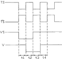
Seeing also Fig. 2, is the working timing figure of this shifting deposit unit 100.In period, the output signal VS of this last shifting deposit unit is a low level by the high level saltus step, the inversion clock signal at t1
 By low transition is high level, and the 3rd transistor P3 and the 4th transistor P4 are ended, and then this first clock
 negative circuit 110 is disconnected.And this clock signal TS is a low level by the high level saltus step, make the 9th transistor P9 and the tenth transistor P10 conducting, and then make this second clock negative circuit 130 conductings, and the high level of this signal output part V original state is through the tenth transistor P10, the 6th transistor P6 is ended, and the low level of the 8th transistor P8 output is via the 9th transistor P9, make the 5th transistor P5 conducting, and then the high level signal VDD that makes its source electrode exports this signal output part V to, thereby this signal output part V keeps high level output.
At t2 in the period, this inversion clock signal
 By the high level saltus step is low level, then makes the 3rd transistor P3 and the 4th transistor P4 conducting, and then makes this first clock negative circuit, 110 conductings.And this clock signal TS is a high level by low transition, and the 9th transistor P9 and the tenth transistor P10 are ended, and then this second clock
 negative circuit 130 is disconnected.This input signal VS is a low level by the high level saltus step, then make this first transistor P1 conducting, the high level VDD of its source electrode ends the 5th transistor P5 through the 3rd transistor P3, and the low level of this input signal VS makes this signal output part V output low level through the 4th transistor P4 conducting the 6th transistor P6.
At t3 in the period, this inversion clock signal
 By low transition is high level, and the 3rd transistor P3 and the 4th transistor P4 are ended, and then this first clock
 negative circuit 110 is disconnected.And this clock signal TS is a low level by the high level saltus step, makes the 9th transistor P9 and the tenth transistor P10 conducting, and then makes this second clock negative circuit 130 conductings.Low level conducting the 7th transistor P7 of this signal output part V, the high level of its source electrode ends the 5th transistor P5 through the 9th transistor P9.Simultaneously, the low level of this signal output part V is also through the tenth transistor P10, conducting the 6th transistor P6, and the drain electrode low level of the 6th transistor P6 makes this signal output part V keep low level output.
At t4 in the period, this inversion clock signal
 By the high level saltus step is low level, then makes the 3rd transistor P3 and the 4th transistor P4 conducting, and then makes this first clock negative circuit, 110 conductings.And this clock signal TS is a high level by low transition, and the 9th transistor P9 and the tenth transistor P10 are ended, and then this second clock
 negative circuit 120 is disconnected.The high level of input signal VS ends the 6th transistor P6 through the 4th transistor P4, and the drain electrode low level of this transistor seconds P2 is through the 3rd transistor P3 conducting the 5th transistor P5, make the high level of its source electrode export this signal output part V to, making the output of this signal output part V is high level by low transition.
From work schedule as seen, the input signal VS of this shifting deposit unit 100 signal that to be last shifting deposit unit export in the period at t1 period and t2, and signal output part V is in t2 period and t3 output signal in the period, input signal VS and output signal are when t2
There is the signal overlap situation in section, and then cause adopting the LCD of this shift register as data drive circuit and scan drive circuit, when carrying out line scanning or column scan, the phenomenon that exists adjacent two row (Row) or row (Column) to scan simultaneously, thereby load signal produces the phase mutual interference, makes picture produce aberration.
Summary of the invention
In order to solve the overlapping problem of above-mentioned shift register output signal, provide the non-overlapping shift register of a kind of output signal real for necessary.
The problem that signal disturbs occurs in order to solve above-mentioned LCD, provide a kind of LCD of avoiding signal to disturb also to be necessity.
A kind of shift register, it comprises a plurality of shifting deposit units, and two clock signals that two adjacent shifting deposit units are received are anti-phase, and each shifting deposit unit includes:
One signal output apparatus, this signal output apparatus receives the clock signal from external circuit, and this signal output apparatus comprises a clock transistor and a level transistor, and this clock transistor is exported this clock signal; The signal of this level transistor output is a permanent low level signal;
One signal input circuit, it receives the output signal of last shifting deposit unit, this clock transistor of conducting, and at this clock transistor conducting one clock after the cycle, the output signal that receives back one shifting deposit unit is with by this clock signal;
One first logical circuit, it receives the signal of this clock signal and the output of this signal input circuit, when this clock transistor conducting, by this level transistor; With
One second logical circuit, it receives the output signal of back one shifting deposit unit, with this level transistor of conducting;
Wherein, export a Continuity signal to this clock transistor and this first logical circuit when this signal input circuit, this first logical circuit is exported a pick-off signal, and by this level transistor, this signal output apparatus is exported this clock signal by this clock transistor; Otherwise, when this signal input circuit output pick-off signal, this clock transistor ends, this second logical circuit is exported a Continuity signal to open this level transistor, this signal output apparatus is output as this perseverance low level signal, and this first logical circuit receives this clock signal to keep this perseverance low level signal output.
A kind of LCD, it comprises: a liquid crystal panel; One data drive circuit, it comprises a shift register; And scan driving circuit, it comprises a shift register; Each shift register comprises: a plurality of shifting deposit units, and two clock signals that two adjacent shifting deposit units are received are anti-phase, and each shifting deposit unit includes:
One signal output apparatus, this signal output apparatus receives the clock signal from external circuit, and this signal output apparatus comprises a clock transistor and a level transistor, and this clock transistor is exported this clock signal; The signal of this level transistor output is a permanent low level signal;
One signal input circuit, it receives the output signal of last shifting deposit unit, this clock transistor of conducting, and at this clock transistor conducting one clock after the cycle, the output signal that receives back one shifting deposit unit is with by this clock signal;
One first logical circuit, it receives the signal of this clock signal and the output of this signal input circuit, when this clock transistor conducting, by this level transistor; With
One second logical circuit, it receives the output signal of back one shifting deposit unit, with this level transistor of conducting;
Wherein, export a Continuity signal to this clock transistor and this first logical circuit when this signal input circuit, this first logical circuit is exported a pick-off signal, and by this level transistor, this signal output apparatus is exported this clock signal by this clock transistor; Otherwise, when this signal input circuit output pick-off signal, this clock transistor ends, this second logical circuit is exported a Continuity signal to open this level transistor, this signal output apparatus is output as this perseverance low level signal, and this first logical circuit receives this clock signal to keep this perseverance low level signal output.
Compared to prior art, during the shifting deposit unit clock signal of shift register of the present invention, can make the opposite clock signal of back one shifting deposit unit output, make this first logical circuit when this clock transistor conducting, by this level transistor, to guarantee that this shifting deposit unit can not export permanent low level signal, then with the output signal zero lap of back one shifting deposit unit.In addition, the input circuit of shifting deposit unit of the present invention links to each other with the output terminal of back one shifting deposit unit, thereby, the signal of shifting deposit unit output is a high level signal after this, can make this shifting deposit unit close this clock transistor, thereby this shifting deposit unit output low level signal is opposite, not overlapping with the signal of this back one shifting deposit unit output.Thereby the LCD that adopts this shift register is when carrying out column scan or line scanning, and its output scanning signal and data-signal can not produce signal and disturb, thereby avoid display frame aberration to occur.
Description of drawings
Fig. 1 is a kind of circuit diagram of shifting deposit unit of prior art shift register.
Fig. 2 is the working timing figure of shifting deposit unit shown in Figure 1.
Fig. 3 is the structural framing figure of shift register one better embodiment of the present invention.
Fig. 4 is the circuit diagram of this first shifting deposit unit and this second shifting deposit unit.
Fig. 5 is the working timing figure of first shifting deposit unit shown in Figure 4 and second shifting deposit unit.
Fig. 6 is a structural representation of using the LCD of shift register shown in Figure 3.
Embodiment
Seeing also Fig. 3, is the structural framing figure of shift register one better embodiment of the present invention.This shift register 20 comprises a plurality of shifting deposit units with same circuits structure, these a plurality of shifting deposit units are connected successively, receive first clock signal clk that external circuit provides and second clock signal CLKB, high level signal VGH and the low level signal VGL anti-phase successively with this first clock signal, and when test acceptance test signal TEST.Each shifting deposit unit is formed by a plurality of nmos type transistors, and each nmos type transistor includes a grid, source electrode and drain electrode.With first shifting deposit unit 21 and second shifting deposit unit 22 that is adjacent is that example illustrates that it is that this first shifting deposit unit 21 comprises an input signal end VIN1, one first output terminal VOUT1 and one second output terminal VOUT2 that being connected of this shift register 20 closes.This second shifting deposit unit 22 comprises a signal input part VIN2, one first output terminal VO1 and one second output terminal VO2.The output signal of the first output terminal VOUT1 of this first shifting deposit unit 21 is as the input signal of the signal input part VIN2 of this second shifting deposit unit 22; Second output terminal VOUT2 of this first shifting deposit unit 21 and this second shifting deposit unit 22 and VO2 are that external circuit (figure does not show) provides signal.
Seeing also Fig. 4, is the circuit diagram that this first shifting deposit unit 21 is connected with this second shifting deposit unit 22.This first shifting deposit unit 21 comprises a signal input circuit 211, one first logical circuit 212, one second logical circuit 213, one the 3rd logical circuit 214, a signal output apparatus 215, a test circuit 216, a first node 1 and a Section Point 2.This first node 1 is the formation that crosses of this signal input circuit 211, this first logical circuit 212, the 3rd logical circuit 214 and this signal output apparatus 215; This Section Point 2 is the formation that crosses of this second logical circuit 213, the 3rd logical circuit 214 and this signal output apparatus 215.
This signal input circuit 211 comprises a first transistor M1 and a transistor seconds M2.The source electrode of this first transistor M1 receives the high level signal VGH from external circuit, and its grid is as the input end VIN1 of this displacement deposit unit 21, and its drain electrode is connected to the source electrode of this transistor seconds M2 and exports this first node 1 in the lump to.The grid of this transistor seconds M2 is connected with the first output terminal VO1 of this second shifting deposit unit 22, and its drain electrode receives the low level signal VGL of external circuit.
This first logical circuit 212 comprises one the 3rd transistor M3, one the 4th transistor M4, one the 5th transistor M5 and one the 6th transistor M6.The grid of the 3rd transistor M3 receives first clock signal clk from external circuit, and its drain electrode receives the high level signal VGH from external circuit, and source electrode is connected with the drain electrode of the 4th transistor M4.The grid of the 4th transistor M4 connects this first node 1, and its source electrode receives the low level signal VGL from external circuit, and its drain electrode is connected to the grid of the 5th transistor M5.The drain electrode of the 5th transistor M5 receives the high level signal VGH from external circuit, and its source electrode is connected to the drain electrode of the 6th transistor M6.The grid of the 6th transistor M6 is connected to the grid of the 4th transistor M4, and its source electrode receives a low level signal VGL from external circuit.
This second logical circuit 213 comprises one the 7th transistor M7.The grid of the 7th transistor M7 is connected with the first output terminal VO1 of this second shifting deposit unit 22, and its drain electrode receives the high level signal VGH from external circuit, and its source electrode is connected to this Section Point 2.
The 3rd logical circuit 214 comprises one the 8th transistor M8 and one the 9th transistor M9.The grid of the 8th transistor M8 is connected to this Section Point 2, and its source electrode links to each other with the drain electrode of the 9th transistor M9, and its drain electrode is connected to this first node 1.The source electrode of the 9th transistor M9 receives outside low level signal VGL.
This signal output apparatus 215 comprises a clock transistor (not indicating), a level transistor (not indicating), one first output terminal VOUT1 and one second output terminal VOUT2.This clock transistor comprises 1 the tenth transistor M10 and 1 the tenth two-transistor M12, and this level transistor comprises 1 the 11 transistor M11 and 1 the 13 transistor M13.The drain electrode of the tenth transistor M10 and the tenth two-transistor M12 all receives first clock signal clk from external circuit, the grid of the two all is connected to this first node 1, the source electrode of the two is connected to the drain electrode of the 11 transistor M11 and the 13 transistor M13 respectively, and respectively as the first output terminal VOUT1 and the second output terminal VOUT2.The grid of the 11 transistor M11 and the 13 transistor M13 all is connected to this Section Point 2, and the source electrode of the two all receives the low level signal VGL that external circuit provides.
This test circuit 216 comprises that the grid of 1 the 14 transistor M14 and a test input 3, the 14 transistor M14 is connected to drain electrode, and should drain electrode as this test input 3, its source electrode is connected to first node 1.
The circuit structure of this second displacement deposit unit 22 is identical with the circuit structure of this first displacement deposit unit 21, and it also comprises 14 transistor T 1~T14, a signal input part VIN2, one first output terminal VO1, one second output terminal VO2.This second displacement deposit unit 22 is with the difference of this first displacement deposit unit 21: the first output terminal VOUT1 that this second shifting deposit unit 22 receives this first shifting deposit unit 21 is as signal input part VIN2, and its first output terminal VO1 is connected with the transistor seconds M2 of this first shifting deposit unit 21 and the grid of the 7th transistor M7; The grid of its 9th transistor T 9 links to each other with the drain electrode of the 7th transistor M7 of this first shifting deposit unit 21; The drain electrode of the grid of its 3rd transistor T 3 and Qi Di ten transistor Ts 10 and the tenth two-transistor T12 all receives the second clock signal CLKB that external circuit provides.
Seeing also Fig. 5, is the working timing figure of this first shifting deposit unit 21 and this second shifting deposit unit 22.Before time period, signal input part VIN1 inserts high level at t1, this first transistor M1 conducting, and then this first node 1 is in high level, thus the tenth transistor M10 and the tenth two-transistor M12 conducting; And make the 6th transistor M6 and the 4th transistor M4 conducting, this low level signal VGL exports the drain electrode of the 3rd transistor M3 to via the 4th transistor M4, and via the 6th transistor M6 output low level signal VGL to this Section Point 2.In time period, this first clock signal clk fades to high level signal VGH by low level signal VGL at t1.The first output terminal VOUT1 of this first shifting deposit unit 21 and the second output terminal VOUT2 all export first clock signal clk that this output circuit 215 receives, promptly export high level signal VGH, this high level signal VGH is sent to the signal receiving end VIN2 of this second shifting deposit unit 22.Simultaneously, this first logical circuit 212 receives this first clock signal clk, opens the 3rd transistor M3, but, the drain electrode of the 3rd transistor M3 receives low level signal VGL, thereby the 5th transistor M5 is ended, and this Section Point 2 keeps low level signal VGL.Thereby, this Section Point 2 output low level signal VGL are to this signal output apparatus 215, the 11 transistor M11 and the 13 transistor M13 end, be not subjected to the source electrode of the 11 transistor M11 and the 13 transistor M13 to connect the influence of low level signal VGL with the signal that guarantees this first output terminal VOUT1 and this second output terminal VOUT2 output, do not produce noise (Ripple).
The second clock signal CLKB that this second shifting deposit unit 22 receives is low level signal VGL; The input end VIN2 of this second shifting deposit unit 22 receives the high level signal VGH of the first output terminal VOUT1 output of this first shifting deposit unit 21, open this first transistor T1, this the first transistor T1 exports this high level signal VGH to open the tenth transistor T 10 and the tenth two-transistor T12, at t1 in the time period, this the first output terminal VO1 and the second output terminal VO2 export this second clock signal CLKB, i.e. low level signal VGL.Simultaneously, CLKB is low level signal VGL because of this second clock signal, so the 3rd transistor T 3 and the 5th transistor T 5 end, the the 4th and the 6th transistor T 4 and T6 open, and output low level signal VGL is by the 11 and the 13 transistor T 11 and T13.The low level signal VGL of these second shift register, 22 outputs is sent to this first shifting deposit unit 21, by its transistor seconds M2, to guarantee that these first shifting deposit unit, 21 first nodes 1 are high level.
In time period, first clock signal clk that this first shifting deposit unit 21 receives is converted to low level signal VGL by high level signal VGH at t2.The signal input part VIN1 of this first shifting deposit unit 21 receives a low level signal VGL, this the first transistor M1 ends, this first node 1 keeps high level, the tenth transistor M10 and the tenth two-transistor M12 are held open state, this the first output terminal VOUT1 and second output terminal VOUT2 clock signal CLK, i.e. the output low level signal VGL.Simultaneously, the 4th transistor M4 and the 6th transistor M6 are held open state, by the 11 and the 13 transistor M11 and M13.
At t2 in the time, the second clock signal CLKB that this second shifting deposit unit 22 receives is converted to high level signal VGH by low level signal VGL, the low level signal VGL of these first shifting deposit unit, 21 outputs imports the signal input part VIN2 of this second shifting deposit unit 22, by this first transistor T1, the maintenance conducting of the tenth transistor T 10 and the tenth two-transistor T12, this first output terminal VO1 and this second output terminal VO2 export this second clock signal CLKB, promptly export high level signal VGH.Simultaneously, this second clock signal CLKB opens the 3rd transistor T 3, because the 4th transistor T 4 and the 6th transistor T 6 keep conducting state, thereby, the signal of importing the 11 transistor T 11 and the 13 transistor T 13 still is low level signal VGL, by the 11 transistor T 11 and the 13 transistor T 13, prevent that the electric signal of this first output terminal VO1 and this second output terminal VO2 output from producing noise, keep output high level signal VGH.
The high level signal VGH of this first output terminal VO1 output feeds back to the grid of the transistor seconds M2 of this first shifting deposit unit 21, so that this signal input circuit 211 output low level signal VGL are to this first node 1, by the tenth transistor M10 and the tenth two-transistor M12.Simultaneously, the high level signal VGH of this first output terminal VO1 output feeds back to the grid of the 7th transistor M7, open the 7th transistor M7, output high level signal VGH is to the 11 transistor M11 and the 13 transistor M13, the 11 transistor M11 and the 13 transistor M13 conducting keep the first output terminal VOUT1 and the second output terminal VOUT2 output low level signal VGL of this first shifting deposit unit 21.
T2 is after the time period, the signal input part VIN1 of this first shifting deposit unit 21 keeps receiving this low level signal VGL, the 4th transistor M4, the 6th transistor M6, the tenth transistor M10 and the tenth two-transistor M12 remain off, the conducting that the clock signal clk that this first logic conversion unit 212 receives keeps the 11 transistor M11 and the 13 transistor M13, this first output terminal VOUT1 and this second output terminal VOUT2 keep output low level signal VGL.In like manner as can be known, t2 is after the time period, and the first output terminal VO1 of this second shifting deposit unit 22 and the second output terminal VO2 keep output low level signal VGL.
The test circuit 216 of this first shifting deposit unit 21 and the test circuit of this second shifting deposit unit 22 be remain off state in normal operation all, work to this shift register 20 does not have influence, after this shift register 20 is applied to drive display panels, when testing this display panels, the conducting just now of the test circuit of this shift register 20.The 3rd logical circuit 214 is as the clear circuit of this first shifting deposit unit 21, before these shift register 20 work, all external reset signal of grid of the 8th transistor M8 of the 3rd logical circuit 214 and the 9th transistor M9 is to these first shifting deposit unit, 21 zero clearings.
From work schedule, because when the clock signal transistor M10 of this first shifting deposit unit 21 and M12 conducting clock signal, the clock signal transistor T 10 of this second shifting deposit unit 22 and T12 conducting, clock signal is because the clock signal that this first shifting deposit unit 21 and second shifting deposit unit 22 receive is opposite, thereby, the signal zero lap of this first shifting deposit unit 21 and 22 outputs of second shifting deposit unit.In addition, the signal of exporting when this second shifting deposit unit 22 is high level signal VGH, the tenth transistor M10 and the tenth two-transistor M12 of this first shifting deposit unit 21 are ended, thereby guarantee this first shifting deposit unit 21 output low level signal VGL, opposite, not overlapping with the signal of these second shifting deposit unit, 22 outputs.
Also have, the tenth transistor M10 of the output circuit 215 of this first shifting deposit unit 21 and the grid of the tenth two-transistor M12 are connected to this first node 1, when first clock signal clk of the tenth transistor M10 and the tenth two-transistor M12 reception fades to high level signal VGH by low level signal VGL, owing to be subjected to the influence of the tenth transistor M10 and the tenth two-transistor M12 endophyte electric capacity, the tenth transistor M10 and the tenth two-transistor M12 grid voltage uprise, and the current potential of this first node 1 is also drawn high.But, the 4th transistor M4 and the 6th transistor M6 of first logical circuit 212 of the present invention are connected in this first node 1, the grid voltage of the 4th transistor M4 and the 6th transistor M6 is also drawn high, the further step-down of drain voltage of the 4th transistor M4 and the 6th transistor M6 then, be subjected to the influence of the 4th transistor M4 and the 6th transistor M6 endophyte electric capacity, its grid voltage is with step-down, feed back to this first node 1, suppressing the threshold voltage shift of the tenth transistor M10 and the tenth two-transistor M12, thereby guarantee that these first shifting deposit unit, 21 outputs are stable.
Seeing also Fig. 6, is the structural representation of using the LCD of shift register 20 shown in Figure 3.This LCD 30 comprises a display panels 31, a data drive circuit 32 and scan driving circuit 33.This display panels 31 comprises that a upper substrate (figure do not show), an infrabasal plate (figure does not show) and are clamped in the liquid crystal layer (figure does not show) between upper substrate and infrabasal plate, and is provided with one in contiguous liquid crystal layer one side of this infrabasal plate and is used to control the thin film transistor (TFT) array (figure does not show) that liquid crystal molecule reverses situation.These scan drive circuit 33 output scanning signals are with the conducting and the cut-off state of the film transistor matrix of controlling this display panels 31, and these data drive circuit 32 outputting data signals are controlled this display panels 31 display variation.This scan drive circuit 33 and this data drive circuit 32 all utilize the output timing of these shift register 20 gated sweep signals and data-signal, thereby control the demonstration of this display panels 31.This shift register 20 can form in same technology with the thin film transistor (TFT) array of this LCD 30.
Because there is not the signal overlap phenomenon in the output of the shifting deposit units at different levels of this shift register 20, thereby make to use this shift register 20 as the LCD 30 of scan drive circuit 32 and data drive circuit 33 when carrying out column scan or line scanning, its output scanning signal and data-signal can not produce signal and disturb, thereby avoid display frame aberration to occur.
Claims (10)
1. shift register, it comprises a plurality of shifting deposit units, it is characterized in that: two clock signals that two adjacent shifting deposit units are received are anti-phase, and each shifting deposit unit includes:
One signal output apparatus, this signal output apparatus receives the clock signal from external circuit, and this signal output apparatus comprises a clock transistor and a level transistor, and this clock transistor is exported this clock signal; The signal of this level transistor output is a permanent low level signal;
One signal input circuit, it receives the output signal of last shifting deposit unit, this clock transistor of conducting, and at this clock transistor conducting one clock after the cycle, the output signal that receives back one shifting deposit unit is with by this clock signal;
One first logical circuit, it receives the signal of this clock signal and the output of this signal input circuit, when this clock transistor conducting, by this level transistor; With
One second logical circuit, it receives the output signal of back one shifting deposit unit, with this level transistor of conducting;
Wherein, export a Continuity signal to this clock transistor and this first logical circuit when this signal input circuit, this first logical circuit is exported a pick-off signal, and by this level transistor, this signal output apparatus is exported this clock signal by this clock transistor; Otherwise, when this signal input circuit output pick-off signal, this clock transistor ends, this second logical circuit is exported a Continuity signal to open this level transistor, this signal output apparatus is output as this perseverance low level signal, and this first logical circuit receives this clock signal to keep this perseverance low level signal output.
2. shift register as claimed in claim 1 is characterized in that: this shifting deposit unit is made up of a plurality of nmos type transistors.
3. shift register as claimed in claim 2 is characterized in that: this signal input circuit, this first logical circuit and this signal output apparatus cross and form a first node; This second logical circuit, the 3rd logical circuit and this signal output apparatus cross and form a Section Point.
4. shift register as claimed in claim 3 is characterized in that: this signal input circuit comprises a first transistor and a transistor seconds; The source electrode of this first transistor receives the high level signal from external circuit, the grid of this first transistor receives last shifting deposit unit output signal, and the drain electrode of this first transistor is connected to the source electrode of this transistor seconds and exports this first node in the lump to; The grid of this transistor seconds receives the output signal of back one shifting deposit unit, and the drain electrode of this transistor seconds receives the low level signal of external circuit.
5. shift register as claimed in claim 3 is characterized in that: this first logical circuit comprises one the 3rd transistor, one the 4th transistor, one the 5th transistor and one the 6th transistor; The 3rd transistorized grid receives the clock signal from external circuit, and the 3rd transistor drain receives the high level signal from external circuit, and the 3rd transistorized source electrode is connected with the 4th transistor drain; The 4th transistorized grid connects this first node, and the 4th transistorized source electrode receives the low level signal from external circuit, and the 4th transistor drain is connected to the 5th transistorized grid; The 5th transistor drain receives the high level signal from external circuit, and the 5th transistorized source electrode is connected to the 6th transistor drain, and receives trigger pip at the corresponding levels; The 6th transistorized grid is connected to the 4th transistorized grid, and the 6th transistorized source electrode receives a low level signal from external circuit.
6. shift register as claimed in claim 3 is characterized in that: this second logical circuit, and this second logical circuit comprises one the 7th transistor; The 7th transistorized grid and back one displacement
 The output terminal of deposit unit connects, and the 7th transistor drain receives the high level signal from external circuit, and the 7th transistorized source electrode receives this trigger pip at the corresponding levels and is connected to this Section Point.
7. shift register as claimed in claim 3 is characterized in that: this shifting deposit unit further comprises one the 3rd logical circuit, and the 3rd logical circuit comprises one the 8th transistor and one the 9th transistor; The 8th transistorized grid is connected to this Section Point, and the 8th transistorized source electrode links to each other with the 9th transistor drain, and the 8th transistor drain is connected to this first node; The 9th transistorized grid receives this higher level's trigger pip, and the 9th transistorized source electrode receives outside low level signal, and the 3rd logical circuit is used for this shift register zero clearing.
8. shift register as claimed in claim 3 is characterized in that: the clock transistor of this signal output apparatus comprises 1 the tenth transistor and 1 the tenth two-transistor, and this level transistor comprises 1 the 11 transistor and 1 the 13 transistor; The drain electrode of the tenth transistor and the tenth two-transistor all receives the clock signal from external circuit, the grid of the two all is connected to this first node, the source electrode of the two is connected to the 11 transistor and the 13 transistor drain respectively, and respectively as one first output terminal and one second output terminal; The 11 transistor and the 13 transistorized grid all are connected to this Section Point, and the source electrode of the two all receives the low level signal that external circuit provides.
9. shift register as claimed in claim 3, it is characterized in that: this shifting deposit unit further comprises a test circuit, this test circuit comprises 1 the 14 transistor, the 14 transistorized grid and the test signal of drain electrode reception from external circuit, the 14 transistorized source electrode is connected to this first node.
10. LCD, it comprises a liquid crystal panel, one data drive circuit, and scan driving circuit, this data drive circuit and this scan drive circuit include a shift register, it is characterized in that: this shift register is any described shift register in the claim 1 to 9.
Priority Applications (2)
| Application Number | Priority Date | Filing Date | Title |
|---|---|---|---|
| CN200710074230A CN100592425C (en) | 2007-04-27 | 2007-04-27 | Shift register and liquid crystal display |
| US12/150,380 US8373637B2 (en) | 2007-04-27 | 2008-04-28 | Shift register and liquid crystal display using same |
Applications Claiming Priority (1)
| Application Number | Priority Date | Filing Date | Title |
|---|---|---|---|
| CN200710074230A CN100592425C (en) | 2007-04-27 | 2007-04-27 | Shift register and liquid crystal display |
Publications (2)
| Publication Number | Publication Date |
|---|---|
| CN101295546A CN101295546A (en) | 2008-10-29 |
| CN100592425C true CN100592425C (en) | 2010-02-24 |
Family
ID=39886349
Family Applications (1)
| Application Number | Title | Priority Date | Filing Date |
|---|---|---|---|
| CN200710074230A Active CN100592425C (en) | 2007-04-27 | 2007-04-27 | Shift register and liquid crystal display |
Country Status (2)
| Country | Link |
|---|---|
| US (1) | US8373637B2 (en) |
| CN (1) | CN100592425C (en) |
Cited By (1)
| Publication number | Priority date | Publication date | Assignee | Title |
|---|---|---|---|---|
| CN102340909A (en) * | 2010-07-23 | 2012-02-01 | 聚积科技股份有限公司 | Serial Controller vs. Serial Bidirectional Controller |
Families Citing this family (18)
| Publication number | Priority date | Publication date | Assignee | Title |
|---|---|---|---|---|
| US8232947B2 (en) * | 2008-11-14 | 2012-07-31 | Semiconductor Energy Laboratory Co., Ltd. | Liquid crystal display device |
| EP2234100B1 (en) | 2009-03-26 | 2016-11-02 | Semiconductor Energy Laboratory Co., Ltd. | Liquid crystal display device |
| KR102071057B1 (en) | 2009-06-25 | 2020-01-29 | 가부시키가이샤 한도오따이 에네루기 켄큐쇼 | Display device |
| CN102097132B (en) * | 2009-12-14 | 2013-11-20 | 群康科技(深圳)有限公司 | Shift register and liquid crystal panel driving circuit |
| WO2011145666A1 (en) * | 2010-05-21 | 2011-11-24 | Semiconductor Energy Laboratory Co., Ltd. | Pulse output circuit, shift register, and display device |
| CN101996605B (en) * | 2010-11-18 | 2013-01-02 | 友达光电股份有限公司 | Gate driving circuit on liquid crystal panel |
| CN102646401B (en) * | 2011-12-30 | 2013-10-16 | 北京京东方光电科技有限公司 | Shift register, global outstanding assessment (GOA) panel and grid electrode driving method |
| CN102651208B (en) | 2012-03-14 | 2014-12-03 | 京东方科技集团股份有限公司 | Grid electrode driving circuit and display |
| KR101394939B1 (en) * | 2012-09-07 | 2014-05-14 | 엘지디스플레이 주식회사 | Shift register |
| TWI473069B (en) * | 2012-12-27 | 2015-02-11 | Innocom Tech Shenzhen Co Ltd | Gate driving device |
| TWI654613B (en) * | 2014-02-21 | 2019-03-21 | 日商半導體能源研究所股份有限公司 | Semiconductor device and electronic device |
| CN104332137B (en) * | 2014-11-28 | 2016-11-16 | 京东方科技集团股份有限公司 | Gate driver circuit and display device |
| CN106601190B (en) * | 2017-03-06 | 2018-12-21 | 京东方科技集团股份有限公司 | Shift register cell and its driving method, gate driving circuit and display device |
| CN107492361B (en) * | 2017-09-26 | 2022-01-11 | 惠科股份有限公司 | Shift register circuit and display panel using same |
| CN108182897B (en) * | 2017-12-28 | 2019-12-31 | 武汉华星光电半导体显示技术有限公司 | Method for testing pixel driving circuit |
| CN109345998B (en) * | 2018-12-20 | 2021-09-03 | Tcl华星光电技术有限公司 | GOA circuit and display panel |
| US11380374B2 (en) * | 2019-07-02 | 2022-07-05 | Boe Technology Group Co., Ltd. | Shift register unit, driving method thereof, and device |
| CN117337457A (en) | 2022-04-28 | 2024-01-02 | 京东方科技集团股份有限公司 | Scanning circuit, display device and method of operating scanning circuit |
Family Cites Families (7)
| Publication number | Priority date | Publication date | Assignee | Title |
|---|---|---|---|---|
| TWI282081B (en) * | 2002-08-13 | 2007-06-01 | Au Optronics Corp | Shift register circuit |
| US7369111B2 (en) * | 2003-04-29 | 2008-05-06 | Samsung Electronics Co., Ltd. | Gate driving circuit and display apparatus having the same |
| US7486269B2 (en) * | 2003-07-09 | 2009-02-03 | Samsung Electronics Co., Ltd. | Shift register, scan driving circuit and display apparatus having the same |
| US6891917B2 (en) * | 2003-08-04 | 2005-05-10 | Atmel Corporation | Shift register with reduced area and power consumption |
| TWI229341B (en) * | 2003-08-13 | 2005-03-11 | Toppoly Optoelectronics Corp | Shift register circuit and a signal-triggered circuit for low temperature poly silicon (LTPS) liquid crystal display |
| US6970530B1 (en) * | 2004-08-24 | 2005-11-29 | Wintek Corporation | High-reliability shift register circuit |
| JP5079301B2 (en) * | 2006-10-26 | 2012-11-21 | 三菱電機株式会社 | Shift register circuit and image display apparatus including the same |
-
2007
- 2007-04-27 CN CN200710074230A patent/CN100592425C/en active Active
-
2008
- 2008-04-28 US US12/150,380 patent/US8373637B2/en not_active Expired - Fee Related
Cited By (2)
| Publication number | Priority date | Publication date | Assignee | Title |
|---|---|---|---|---|
| CN102340909A (en) * | 2010-07-23 | 2012-02-01 | 聚积科技股份有限公司 | Serial Controller vs. Serial Bidirectional Controller |
| CN102340909B (en) * | 2010-07-23 | 2014-01-15 | 聚积科技股份有限公司 | Serial Controller vs. Serial Bidirectional Controller |
Also Published As
| Publication number | Publication date |
|---|---|
| CN101295546A (en) | 2008-10-29 |
| US20080266234A1 (en) | 2008-10-30 |
| US8373637B2 (en) | 2013-02-12 |
Similar Documents
| Publication | Publication Date | Title |
|---|---|---|
| CN100592425C (en) | Shift register and liquid crystal display | |
| CN101388253B (en) | Shifting register and LCD | |
| CN101377956B (en) | Shift register and LCD | |
| CN101359511B (en) | Shift register and liquid crystal display using the shift register | |
| CN101206318B (en) | Shifting register and LCD device | |
| CN104658506B (en) | Shift register, gate driving circuit and its driving method, display panel | |
| JP6114378B2 (en) | Shift register element, driving method thereof, and display device including shift register | |
| CN104078017B (en) | Shift register cell, gate driver circuit and display unit | |
| CN106251804B (en) | Shift register cell, driving method, gate driving circuit and display device | |
| CN107767809B (en) | Drive element of the grid, driving method and gate driving circuit | |
| US20190005866A1 (en) | Shift Register Unit, Driving Method, Gate Driver on Array and Display Device | |
| CN101241765A (en) | Shift register and LCD device | |
| US11410608B2 (en) | Shift register circuitry, gate driving circuit, display device, and driving method thereof | |
| US20140085283A1 (en) | Gate Driving Circuit And Display | |
| CN109935209A (en) | Shift register cell, gate driving circuit, display device and driving method | |
| JP2021534530A (en) | Shift register unit, gate drive circuit, display device and drive method | |
| CN101339810B (en) | Shift register and LCD device using the same | |
| CN105096865A (en) | Shift register output control unit, shift register and drive method thereof and grid drive device | |
| US20210366401A1 (en) | Shift register unit, gate drive circuit and drive method | |
| CN109410810B (en) | Shift register unit and driving method thereof, gate driving circuit and display device | |
| CN101241247A (en) | Shift registers and LCD device | |
| CN105654991A (en) | Shifting register, driving method thereof, GOA circuit and display device | |
| CN103021321A (en) | Shift register and liquid crystal display device | |
| CN101593561B (en) | LCD Monitor | |
| CN108877659B (en) | Gate driving circuit, display device and driving method thereof |
Legal Events
| Date | Code | Title | Description |
|---|---|---|---|
| C06 | Publication | ||
| PB01 | Publication | ||
| C10 | Entry into substantive examination | ||
| SE01 | Entry into force of request for substantive examination | ||
| C14 | Grant of patent or utility model | ||
| GR01 | Patent grant |