CN101005014A - Semiconductor device fabrication equipment and method of using the same - Google Patents
Semiconductor device fabrication equipment and method of using the same Download PDFInfo
- Publication number
- CN101005014A CN101005014A CNA2007100042235A CN200710004223A CN101005014A CN 101005014 A CN101005014 A CN 101005014A CN A2007100042235 A CNA2007100042235 A CN A2007100042235A CN 200710004223 A CN200710004223 A CN 200710004223A CN 101005014 A CN101005014 A CN 101005014A
- Authority
- CN
- China
- Prior art keywords
- duration
- unit
- wafer
- substrate
- speed
- Prior art date
- Legal status (The legal status is an assumption and is not a legal conclusion. Google has not performed a legal analysis and makes no representation as to the accuracy of the status listed.)
- Pending
Links
Images


Classifications
-
- H—ELECTRICITY
- H10—SEMICONDUCTOR DEVICES; ELECTRIC SOLID-STATE DEVICES NOT OTHERWISE PROVIDED FOR
- H10P—GENERIC PROCESSES OR APPARATUS FOR THE MANUFACTURE OR TREATMENT OF DEVICES COVERED BY CLASS H10
- H10P95/00—Generic processes or apparatus for manufacture or treatments not covered by the other groups of this subclass
-
- H—ELECTRICITY
- H10—SEMICONDUCTOR DEVICES; ELECTRIC SOLID-STATE DEVICES NOT OTHERWISE PROVIDED FOR
- H10P—GENERIC PROCESSES OR APPARATUS FOR THE MANUFACTURE OR TREATMENT OF DEVICES COVERED BY CLASS H10
- H10P72/00—Handling or holding of wafers, substrates or devices during manufacture or treatment thereof
- H10P72/04—Apparatus for manufacture or treatment
- H10P72/0451—Apparatus for manufacturing or treating in a plurality of work-stations
- H10P72/0468—Apparatus for manufacturing or treating in a plurality of work-stations comprising a chamber adapted to a particular process
- H10P72/0474—Apparatus for manufacturing or treating in a plurality of work-stations comprising a chamber adapted to a particular process comprising at least one lithography chamber
-
- G—PHYSICS
- G05—CONTROLLING; REGULATING
- G05B—CONTROL OR REGULATING SYSTEMS IN GENERAL; FUNCTIONAL ELEMENTS OF SUCH SYSTEMS; MONITORING OR TESTING ARRANGEMENTS FOR SUCH SYSTEMS OR ELEMENTS
- G05B19/00—Program-control systems
- G05B19/02—Program-control systems electric
- G05B19/418—Total factory control, i.e. centrally controlling a plurality of machines, e.g. direct or distributed numerical control [DNC], flexible manufacturing systems [FMS], integrated manufacturing systems [IMS] or computer integrated manufacturing [CIM]
- G05B19/41865—Total factory control, i.e. centrally controlling a plurality of machines, e.g. direct or distributed numerical control [DNC], flexible manufacturing systems [FMS], integrated manufacturing systems [IMS] or computer integrated manufacturing [CIM] characterised by job scheduling, process planning, material flow
-
- H—ELECTRICITY
- H10—SEMICONDUCTOR DEVICES; ELECTRIC SOLID-STATE DEVICES NOT OTHERWISE PROVIDED FOR
- H10P—GENERIC PROCESSES OR APPARATUS FOR THE MANUFACTURE OR TREATMENT OF DEVICES COVERED BY CLASS H10
- H10P72/00—Handling or holding of wafers, substrates or devices during manufacture or treatment thereof
- H10P72/06—Apparatus for monitoring, sorting, marking, testing or measuring
- H10P72/0612—Production flow monitoring, e.g. for increasing throughput
-
- G—PHYSICS
- G05—CONTROLLING; REGULATING
- G05B—CONTROL OR REGULATING SYSTEMS IN GENERAL; FUNCTIONAL ELEMENTS OF SUCH SYSTEMS; MONITORING OR TESTING ARRANGEMENTS FOR SUCH SYSTEMS OR ELEMENTS
- G05B2219/00—Program-control systems
- G05B2219/30—Nc systems
- G05B2219/32—Operator till task planning
- G05B2219/32247—Real time scheduler
-
- G—PHYSICS
- G05—CONTROLLING; REGULATING
- G05B—CONTROL OR REGULATING SYSTEMS IN GENERAL; FUNCTIONAL ELEMENTS OF SUCH SYSTEMS; MONITORING OR TESTING ARRANGEMENTS FOR SUCH SYSTEMS OR ELEMENTS
- G05B2219/00—Program-control systems
- G05B2219/30—Nc systems
- G05B2219/45—Nc applications
- G05B2219/45031—Manufacturing semiconductor wafers
-
- Y—GENERAL TAGGING OF NEW TECHNOLOGICAL DEVELOPMENTS; GENERAL TAGGING OF CROSS-SECTIONAL TECHNOLOGIES SPANNING OVER SEVERAL SECTIONS OF THE IPC; TECHNICAL SUBJECTS COVERED BY FORMER USPC CROSS-REFERENCE ART COLLECTIONS [XRACs] AND DIGESTS
- Y02—TECHNOLOGIES OR APPLICATIONS FOR MITIGATION OR ADAPTATION AGAINST CLIMATE CHANGE
- Y02P—CLIMATE CHANGE MITIGATION TECHNOLOGIES IN THE PRODUCTION OR PROCESSING OF GOODS
- Y02P90/00—Enabling technologies with a potential contribution to greenhouse gas [GHG] emissions mitigation
- Y02P90/02—Total factory control, e.g. smart factories, flexible manufacturing systems [FMS] or integrated manufacturing systems [IMS]
Landscapes
- Engineering & Computer Science (AREA)
- General Engineering & Computer Science (AREA)
- Manufacturing & Machinery (AREA)
- Quality & Reliability (AREA)
- Physics & Mathematics (AREA)
- General Physics & Mathematics (AREA)
- Automation & Control Theory (AREA)
- Exposure And Positioning Against Photoresist Photosensitive Materials (AREA)
- Exposure Of Semiconductors, Excluding Electron Or Ion Beam Exposure (AREA)
Abstract
本发明提供了半导体器件制造设备和使用该设备的方法,所述设备和方法使晶圆通过所述设备传送所花费的总时间最小化,并使晶圆在设备的各个部分之间传送的次数最小化。半导体器件制造设备包括:第一装置,用于对晶圆执行第一工序;第二装置,与第一装置联机连接,并用于执行相对于由晶圆组成的半导体器件的制造的第一工序后续的第二工序;速度调节器,连接到第一装置和第二装置。速度调节器分别检测第一工序和第二工序的持续时间,比较持续时间,确定第一工序的持续时间是否短于第二工序的持续时间。速度调节器还被构造为当第一工序的持续时间短于第二工序的持续时间时调节执行第一工序的速度。
The present invention provides semiconductor device fabrication equipment and methods of using the same that minimize the total time a wafer takes to transport through the equipment and the number of times a wafer is transported between various parts of the equipment minimize. The semiconductor device manufacturing apparatus includes: a first device for performing a first process on a wafer; a second device connected in-line with the first device and for performing subsequent steps relative to the first process of manufacturing a semiconductor device composed of a wafer. The second process; a speed regulator, connected to the first device and the second device. The speed regulator respectively detects the duration of the first process and the second process, compares the durations, and determines whether the duration of the first process is shorter than the duration of the second process. The speed regulator is also configured to adjust the speed at which the first procedure is performed when the duration of the first procedure is shorter than the duration of the second procedure.
Description
技术领域technical field
本发明涉及制造器件(如半导体器件)的方法和设备。更具体地讲,本发明涉及其中联机(in-line)连接多个装置的制造设备(如照相平板印刷设备)和使用该制造设备处理基板的方法。The present invention relates to methods and apparatus for fabricating devices, such as semiconductor devices. More particularly, the present invention relates to a manufacturing apparatus, such as a photolithography apparatus, in which a plurality of devices are connected in-line and a method of processing a substrate using the manufacturing apparatus.
背景技术Background technique
基本上,通过对晶圆(wafer)重复执行多个单独的工序(如光致抗蚀剂涂覆工序、曝光工序、显影工序、蚀刻工序和沉积工序)来制造半导体器件。因此,制造半导体器件通常需要多个半导体器件制造装置,而每个装置用于执行若干单独的工序。Basically, a semiconductor device is manufactured by repeatedly performing a plurality of individual processes such as a photoresist coating process, an exposure process, a development process, an etching process, and a deposition process on a wafer. Therefore, manufacturing a semiconductor device generally requires a plurality of semiconductor device manufacturing apparatuses, each apparatus for performing several separate processes.
近来,已经提出了各种技术来提高半导体器件的成品率和可靠性。其中一个技术是通过连接多个半导体制造装置来构建自动化的生产线。适于在自动化的生产线中使用的半导体制造设备的一个示例是照相平板印刷设备。照相平板印刷设备用于形成半导体器件的精细图案(如电路图案)。因此,照相平板印刷设备包括:旋涂机(spinner),用光致抗蚀剂层涂覆晶圆,并且一旦晶圆已经曝光,用显影溶液涂覆曝光的晶圆以使光致抗蚀剂显影;曝光装置,与旋涂机联机连接,用于使其上已经形成光致抗蚀剂层的晶圆曝光;传送装置,位于旋涂机和曝光装置之间。传送装置包括缓冲器和用于将晶圆从旋涂机经缓冲器传送到曝光装置的机器人(robot),从而使生产线自动化。Recently, various techniques have been proposed to improve the yield and reliability of semiconductor devices. One of these technologies is to construct an automated production line by connecting multiple semiconductor manufacturing devices. One example of semiconductor manufacturing equipment suitable for use in an automated production line is photolithography equipment. Photolithography apparatuses are used to form fine patterns (such as circuit patterns) of semiconductor devices. Thus, photolithography equipment includes: a spinner, coating the wafer with a layer of photoresist, and once the wafer has been exposed, coating the exposed wafer with a developing solution so that the photoresist developing; an exposure device, connected in-line with the spin coater, for exposing the wafer on which a photoresist layer has been formed; a transfer device, located between the spin coater and the exposure device. The transfer device includes a buffer and a robot for transferring the wafer from the spin coater to the exposure device through the buffer, thereby automating the production line.
然而,在照相平板印刷设备的情况下,完成旋涂机中的工序所需的时间与完成曝光装置中的工序所需的时间可能不同。例如,旋涂机涂覆晶圆所花费的时间可少于曝光装置照射(曝光)晶圆所花费的时间。在这种情况下,在使晶圆曝光的同时,传送装置的机器人连续地将若干已涂覆的晶圆从旋涂机装载到缓冲器。在晶圆被曝光后,传送装置的机器人搜索第一个装载到缓冲器中的晶圆,然后将该晶圆传送到曝光装置。However, in the case of a photolithography apparatus, the time required to complete the process in the spin coater may differ from the time required to complete the process in the exposure apparatus. For example, the time it takes for a spin coater to coat a wafer may be less than the time it takes for an exposure device to irradiate (expose) the wafer. In this case, the robot of the conveyor loads several coated wafers from the spin coater to the buffer in succession while exposing the wafers. After the wafers are exposed, the robot of the transfer unit searches for the first wafer loaded into the buffer and transfers that wafer to the exposure unit.
而且,在半导体器件制造设备(如照相平板印刷设备)中,执行第一工序所花费的时间少于执行后续工序所花费的时间,将晶圆传送到缓冲器和从缓冲器传送晶圆花费大量的设备运行时间。即,这种设备的产量低。此外,晶圆必须通过设备的相对大量的单元。因此,晶圆容易被划伤或损坏。Also, in semiconductor device manufacturing equipment such as photolithography equipment, the time it takes to perform the first process is less than the time it takes to perform subsequent processes, it takes a lot of time to transfer the wafer to and from the buffer. equipment running time. That is, the yield of such an apparatus is low. Furthermore, the wafer must pass through a relatively large number of cells of the device. Therefore, the wafer is easily scratched or damaged.
发明内容Contents of the invention
本发明的目标是提供制造设备和使用该设备的方法,所述设备和方法通过在设备中联机连接的处理装置能够将基板的总传送时间最小化。It is an object of the present invention to provide a manufacturing device and a method of using the same, which are capable of minimizing the total transfer time of substrates by processing means connected in-line in the device.
本发明的另一目标是提供一种制造设备和使用该设备的方法,当所述设备包括联机连接的处理装置时,所述设备和方法能够使基板传送到所述设备的部分和传送出所述设备的部分的次数最小化。Another object of the present invention is to provide a manufacturing apparatus and a method of using the apparatus which, when said apparatus comprises processing means connected in-line, enable the transfer of substrates to and from parts of said apparatus. The number of parts of the device described above is minimized.
根据本发明的第一方面,提供了一种制造设备,该设备包括:第一装置,具有第一工序执行部分,所述第一工序执行部分对基板执行第一工序;第二装置,与所述第一装置联机连接,并包括对所述基板执行后续第二工序的单元;速度调节器,可操作地连接到所述第一装置和所述第二装置。所述速度调节器分别检测所述第一工序和所述第二工序的持续时间,并被构造为将所述持续时间进行比较。所述速度调节器还被构造为当所述第一工序的持续时间短于所述第二工序的持续时间时,对所述第一装置发布控制信号,以调节执行所述第一工序的速度。According to the first aspect of the present invention, there is provided a manufacturing equipment, which includes: a first device having a first process execution part, the first process execution part executes a first process on a substrate; a second device, and the The first device is connected in-line, and includes a unit for performing a subsequent second process on the substrate; a speed regulator, operatively connected to the first device and the second device. The speed regulator detects the duration of the first process and the second process, respectively, and is configured to compare the durations. The speed regulator is further configured to issue a control signal to the first device to adjust the speed at which the first procedure is performed when the duration of the first procedure is shorter than the duration of the second procedure .
所述第一工序执行部分可包括至少两个单元和机器人,所述至少两个单元各执行所述第一工序的执行中的步骤,机器人具有包围至少两个单元的工作包络面(working envelope)。因此,机器人将基板从所述至少两个单元中的一个单元传送到另一单元。在这种情况下,所述速度调节器可操作地连接到所述机器人,以控制所述机器人传送基底的时间。The first process execution part may include at least two units and a robot, the at least two units each perform a step in the execution of the first process, and the robot has a working envelope surrounding the at least two units. ). Thus, the robot transfers the substrate from one of the at least two units to the other unit. In this case, the speed regulator is operatively connected to the robot to control when the robot transfers the substrate.
所述第一装置可以是照相平板印刷设备的旋涂装置,所述第二装置可以是照相平板印刷设备的曝光装置。在这种情况下,所述第一工序执行部分包括具有旋转卡盘、光致抗蚀剂的源、连接到所述光致抗蚀剂的源的供应喷嘴的旋涂单元,所述曝光装置包括曝光单元,所述曝光单元包括光源、用于支撑将被曝光的基板的基板台、用于支撑掩模版的掩模版台。此外,所述旋涂装置还可包括对所述基板执行第三工序的第二工序执行部分。具体地讲,所述第二工艺执行部分执行显影工艺。为此,所述第二工序执行部分包括具有旋转卡盘、显影溶液的源、连接到所述显影溶液的源的供应喷嘴的旋涂单元。The first device may be a spin-coating device of a photolithographic apparatus, and the second apparatus may be an exposure apparatus of a photolithographic apparatus. In this case, the first process performing part includes a spin coating unit having a spin chuck, a source of photoresist, a supply nozzle connected to the source of photoresist, and the exposure device An exposure unit is included, and the exposure unit includes a light source, a substrate stage for supporting a substrate to be exposed, and a reticle stage for supporting a reticle. In addition, the spin coating apparatus may further include a second process performing part performing a third process on the substrate. Specifically, the second process performing part performs a developing process. To this end, the second process performing part includes a spin coating unit having a spin chuck, a source of developing solution, a supply nozzle connected to the source of developing solution.
根据本发明的另一方面,提供了一种制造设备,包括:多个装置,相互联机连接,从形成自动化的生产线;速度调节器,可操作地连接到所述装置。所述装置包括分别对基底执行连续工序的至少三个单元。所述速度调节器可操作为分别检测连续工序的持续时间,并被构造为比较所述持续时间。所述速度调节器还被构造为当所达工序的持续时间短于在所述工序的后续执行的工序的持续时间时,对所述执行所述工序中的一个的装置发布信号,以调节执行所述工序的速度。According to another aspect of the present invention, there is provided a manufacturing facility, comprising: a plurality of devices connected in-line with each other to form an automated production line; a speed regulator operatively connected to the devices. The apparatus includes at least three units respectively performing successive processes on the substrate. The speed regulator is operable to respectively detect the duration of successive processes and is configured to compare said durations. Said speed regulator is further configured to issue a signal to said means performing one of said procedures to adjust the execution of said procedure when the duration of said procedure is shorter than the duration of a procedure performed subsequent to said procedure. the speed of the process.
根据本发明的第三方面,提供了一种制造方法,该方法包括:利用第一工序装置对基板执行第一工序;利用与所述第一工序装置连接的第二工序装置对所述基板执行所述第一工序后续的第二工序;分别检测所述第一工序和所述第二工序的持续时间,并比较所述持续时间;确定第一工序的持续时间是否短于所述第二工序的持续时间。另外,当确定所述第一工序的持续时间短于所述第二工序的持续时间时,调节执行所述第一工序的速度。According to a third aspect of the present invention, there is provided a manufacturing method, the method comprising: using a first process device to perform a first process on a substrate; using a second process device connected to the first process device to perform a process on the substrate A second process following the first process; respectively detecting the duration of the first process and the second process, and comparing the duration; determining whether the duration of the first process is shorter than the second process duration. In addition, when it is determined that the duration of the first procedure is shorter than the duration of the second procedure, the speed at which the first procedure is performed is adjusted.
可以分别在第一工序装置的至少两个单元中执行执行第一工序的各个步骤。在这种情况下,将基板从所述单元中的至少一个传送到所述单元中的其它。另外,通过延迟基板从所述单元中的一个到所述单元中的另一个的传送来对执行第一工序的速度进行调整。可选择地,通过延迟基板从所述第一工序装置的所述单元中的一个到所述第二工序装置的传送来对执行第一工序的速度进行调整。优选地,调整执行第一工序的速度,使得第一工序的持续时间等于第二工序的时序时间。The respective steps of performing the first process may be performed in at least two units of the first process apparatus, respectively. In this case, the substrate is transferred from at least one of the units to the other of the units. In addition, the speed at which the first process is performed is adjusted by delaying the transfer of the substrate from one of the units to the other of the units. Optionally, the speed at which the first process is performed is adjusted by delaying the transfer of a substrate from one of said cells of said first process device to said second process device. Preferably, the speed of executing the first process is adjusted so that the duration of the first process is equal to the sequence time of the second process.
根据本发明的又一方面,第一工序包括用于光致抗蚀剂涂覆晶圆,所述第二工序包括将所述晶圆曝光于通过掩模版引导的光。此外,优选地可使用第一工序装置来执行使曝光的晶圆显影的第三工序。在这种情况下,检测所述第三工序的持续时间,比较所述第二工序和所述第三工序的持续时间,确定所述第二工序的持续时间是否短于所述第三工序的持续时间。另外,当所述第二工序的持续时间短于所述第三工序的持续时间时调节执行所述第二工序的速度。优选地,调节执行所述第二工序的速度,使得所述第二工序的持续时间等于所述第三工序的持续时间。According to yet another aspect of the invention, the first process includes coating a wafer with photoresist, and the second process includes exposing the wafer to light directed through a reticle. Furthermore, the third process of developing the exposed wafer may preferably be performed using the first process equipment. In this case, detecting the duration of the third process, comparing the duration of the second process and the third process, determining whether the duration of the second process is shorter than the duration of the third process duration. In addition, the speed at which the second procedure is performed is adjusted when the duration of the second procedure is shorter than the duration of the third procedure. Preferably, the speed at which said second procedure is performed is adjusted such that the duration of said second procedure is equal to the duration of said third procedure.
附图说明Description of drawings
通过下面对如附图中所示的本发明的优选实施例进行的详细描述,本发明的上述和其他目的、特征和优点将会变得清楚。附图并不一定是按比例的,重点是示出本发明的原理。The above and other objects, features and advantages of the present invention will become apparent from the following detailed description of preferred embodiments of the present invention as shown in the accompanying drawings. The drawings are not necessarily to scale, emphasis instead being placed upon illustrating the principles of the invention.
图1是根据本发明的半导体器件制造设备的实施例的示意图。FIG. 1 is a schematic diagram of an embodiment of a semiconductor device manufacturing apparatus according to the present invention.
图2是图1中示出的半导体器件制造设备的方框图。FIG. 2 is a block diagram of the semiconductor device manufacturing apparatus shown in FIG. 1. Referring to FIG.
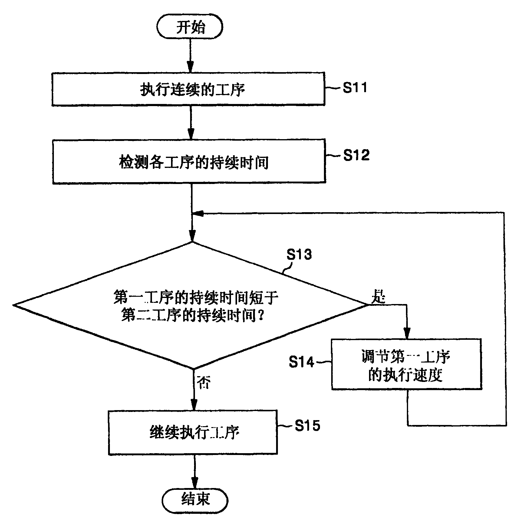
图3是示出根据本发明的制造方法的流程图。FIG. 3 is a flowchart illustrating a manufacturing method according to the present invention.
图4是示出根据本发明的包括照相平板印刷的制造方法的流程图。FIG. 4 is a flowchart illustrating a manufacturing method including photolithography according to the present invention.
具体实施方式Detailed ways
以下,将参照附图更充分地描述本发明。在此,图1和图2中相同的标号表示相同的构件。Hereinafter, the present invention will be more fully described with reference to the accompanying drawings. Here, the same reference numerals in FIG. 1 and FIG. 2 denote the same components.
参照图1和图2,本发明的半导体器件制造设备包括至少两个联机连接的用于执行连续工序的独立(self-contained)装置。例如,半导体器件制造设备可以是照相平板印刷设备100。照相平板印刷设备100包括:旋涂装置110,用光致抗蚀剂涂覆未曝光的晶圆并用显影溶液涂覆已曝光的晶圆;曝光装置150,与旋涂装置110联机连接,用于将已经在旋涂装置110中被涂覆有光致抗蚀剂的晶圆曝光;传送装置130,位于旋涂装置110和曝光装置150之间并连接旋涂装置110和曝光装置150;速度调节器170,用于检测装置110和150执行各自的工序所花费的时间并调节这些时间。更具体地讲,旋涂装置110包括:晶圆装载/卸载部分111;第一工序执行部分117,用光致抗蚀剂涂覆晶圆;第二工序执行部分119,用于使在曝光装置150中曝光的晶圆显影;中央控制单元114,用于控制旋涂装置110的整体操作。Referring to FIGS. 1 and 2, the semiconductor device manufacturing apparatus of the present invention includes at least two self-contained devices connected in-line for performing continuous processes. For example, the semiconductor device manufacturing apparatus may be the
晶圆装载/卸载部分111包括:装载单元112,在装载单元112,将被涂覆、曝光和显影的晶圆被装载到设备100中;卸载单元113,从该卸载单元113将已涂覆、曝光和显影的晶圆从设备100卸载;传送机器人115,将晶圆从装载单元112传送到第一工序执行部分117并将晶圆从第二工序执行部分119传送到卸载单元113,所有这些均受中央控制单元114的控制。装载单元112可包括多个装载台(loading station)。优选地,装载单元112包括第一装载台112a和第二装载台112b。另外,卸载单元113也可包括多个卸载台。优选地,卸载单元113包括第一卸载台113a和第二卸载台113b。在任何情况下,装载单元112和卸载单元113各包括至少一个用于贮存多个晶圆(例如,大约25个晶圆)的晶圆盒和用于晶圆盒的支撑件。The wafer loading/
第一工序执行部分117包括:至少一个旋涂单元117a,用光致抗蚀剂涂覆晶圆;至少一个烘焙单元117b,用于烘焙通过旋涂单元117a在晶圆上形成的光致抗蚀剂的层;传送机器人117e,从装载单元112接收晶圆,将晶圆传送到旋涂单元117a,然后将晶圆从旋涂单元117a传送到烘焙单元117b,所有这些均受中央控制单元114的控制。旋涂单元117a可包括:卡盘,用于将晶圆固定在一定位置并使晶圆旋转;光致抗蚀剂的供应件;喷嘴,用于将光致抗蚀剂供给到旋转的晶圆上。烘焙单元117b可包括在其上安装晶圆的盘和加热该盘的加热器。The first
第一工序执行单元117还可包括:至少一个粘合剂涂覆单元117c,用于在用光致抗蚀剂涂覆晶圆之前将粘合剂涂覆在晶圆上,以提高光致抗蚀剂粘附到晶圆上的能力;至少一个冷却单元117d,用于将加热的晶圆冷却到室温。在这种情况下,粘合剂涂覆单元117c可包括:盘,在该盘上安装晶圆;粘合剂的源;注射喷嘴,用于将粘合剂供给到安装在盘上的晶圆上;加热器,选择性地加热该盘。粘合剂可以是六甲基二硅胺烷(hexamethyldisilazan,HMDS)。冷却单元117d可包括:盘,在该盘上安装晶圆;温度调节器,用于调节盘的温度以降低晶圆的温度并将晶圆保持在室温。因此,由烘焙单元117b加热的晶圆可由冷却单元117d冷却。The first
第二工序执行部分119包括:至少一个显影单元119a,用于将显影溶液供给到曝光的晶圆上以使晶圆显影;至少一个烘焙单元119b,用于烘焙显影的或曝光的晶圆;传送机器人119e,从传送装置130接收晶圆,然后将曝光的或显影的晶圆传送到烘焙单元119b,所有这些均受中央控制单元114的控制。显影单元119a可包括:卡盘,用于固定并旋转晶圆;显影溶液的供应件;喷嘴,用于将显影溶液提供到旋转的晶圆上。烘焙单元119b可包括:盘,在该盘上安装晶圆;加热器,用于加热该盘。因此,可以将在显影单元119a中显影的晶圆或者在曝光装置150中曝光的晶圆传送到烘焙单元119b,然后进行烘焙。The second
第二工序执行部分119还可以包括:至少一个冷却单元119c,用于冷却晶圆;至少一个边缘曝光单元119d,用于使晶圆的边缘曝光。在这种情况下,冷却单元119c可包括:盘,在其上安装晶圆;温度调节器,用于调节盘的温度以将晶圆冷却到室温并使晶圆保持在室温。边缘曝光单元119d可包括:卡盘,用于固定并旋转晶圆;光源,用光源发射的光照射旋转的晶圆的边缘。因此,可以通过边缘曝光单元119d使传送到第二工序执行部分119的晶圆的边缘曝光,并可以通过冷却单元119c将在烘焙单元119b中烘焙的晶圆冷却到室温。The second
除了控制旋涂装置的总体操作之外,中央控制单元114还响应从速度调节器170发送的信号来控制第一工序执行部分117和第二工序执行部分119,以调节第一工序执行部分117执行涂覆工序的速度和第二工序执行部分119执行显影工序的速度。例如,中央控制单元114调节执行涂覆工序的速度,使得第一工序执行部分117执行涂覆工序所花费的时间等于第二工序执行部分119执行后续显影工序所花费的时间。In addition to controlling the overall operation of the spin coating apparatus, the central control unit 114 also controls the first
曝光装置150包括:预对准单元156,用于在曝光之前使晶圆对准;曝光单元154,用于使预对准的晶圆曝光;传送机器人152,从传送装置130接收晶圆,然后将晶圆传送到预对准单元156和曝光单元154;曝光控制单元151,用于控制曝光装置150的总体操作。The
更具体地讲,预对准单元156包括:卡盘,用于将晶圆固定在一定位置并旋转晶圆;光传感器,用于检测基准点(如晶圆中的凹槽(notch)或晶圆中的平坦区(flat zone))。预对准单元156在通过卡盘旋转晶圆的同时检测基准点,然后使卡盘停止,使得基准点面向预定的方向。因此,晶圆与曝光单元154对准。More specifically, the
曝光单元154包括:基板台,在其上安装晶圆;光源,用于发射预定波长的光;掩模版台(reticle stage)和由所述掩模版台支撑的掩模版,位于从光源到基板台延伸的光路上。掩模版具有与将例如形成在晶圆上的电路图案对应的预定图案。曝光单元154引导预定波长的光通过掩模版,并引导至安装在基板台上的晶圆上。结果,掩模版图案的图像被转印到晶圆上的光致抗蚀剂层。即,使晶圆曝光。The
传送机器人152传送曝光装置150中的晶圆。具体地讲,传送机器人152将晶圆从传送装置130传送到预对准单元156,然后将预对准单元156中对准的晶圆传送到曝光单元154。另外,传送机器人152将曝光单元154中曝光的晶圆传送回传送装置130。The
曝光控制单元151与预对准单元156、曝光单元154、传送机器人152连接,并控制曝光装置150的整体操作。另外,曝光控制单元151响应从速度调节器170发送的信号来控制预对准单元156、曝光单元154和传送机器人152,以调节在曝光装置150中执行曝光工序所花费的时间。例如,曝光控制单元151调节执行曝光工序的速度,使得执行曝光工序所花费的时间等于旋涂装置110执行后续的显影工序所花费的时间。The exposure control unit 151 is connected with the
如上所述,传送装置130在旋涂装置110和曝光装置150之间传送晶圆。为此,传送装置130可包括在旋涂装置110和曝光装置150之间往复的传送机器人135和用于控制传送机器人135的操作的接口(interface)控制单元132。As described above, the
可选择地,照相平板印刷设备100可省略传送装置130。即,旋涂装置110和曝光装置150可相互直接连接。在这种情况下,旋涂装置110的第一工序执行部分117的传送机器人117e将晶圆直接传送到曝光装置150的传送机器人152,并且曝光装置150的传送机器人152将晶圆直接传送到旋涂装置110的第二工序执行部分119的传送机器人119e。Alternatively, the
速度调节器170调节照相平板印刷设备100的所有部分的运行时间。为此,速度调节器170可包括:工序持续时间(duration)检测部分172,与装置110和150连接以实时检测装置110和150执行在装置中发生的各工序所花费的时间;速度控制器174,用于响应由工序持续时间检测部分172检测到的信息来控制执行各工序的速度。另外,速度调节器170还可包括工序持续时间存储部分176,用于存储装置110和150执行的各自的工序的持续时间。在这种情况下,在控制随后执行的工序中的任何一个的速度之前,照相平板印刷设备100必须执行所有的工序至少一次。Speed regulator 170 regulates the runtime of all parts of
速度调节器170本质上是本领域普通技术人员利用传统技术可以实现的类型的自动机械控制器。例如,速度调节器170的工序持续时间检测部分172可通过使用由旋涂装置110、传送装置130和曝光装置150的控制单元114、132和151触发的计数器来实现。速度调节器170的工序持续时间存储部分176可被实现为电子存储器器件。速度控制器174可被实现为包含用于比较存储在工序持续时间存储部分176中的数据的比较器的数据处理器。The speed regulator 170 is essentially a robotic controller of the type that can be implemented by one of ordinary skill in the art using conventional techniques. For example, the process duration detection part 172 of the speed regulator 170 may be realized by using counters triggered by the control units 114 , 132 and 151 of the
以下,将参照图3来描述根据本发明的处理基板的一般方法。Hereinafter, a general method of processing a substrate according to the present invention will be described with reference to FIG. 3 .
首先,基板(如半导体晶圆)要经过多个连续的工序(S11)。First, a substrate (such as a semiconductor wafer) is subjected to a plurality of consecutive processes (S11).
这时,监控这些工序,检测并量化这些工序的各自持续时间(S12)。工序的持续时间可被限定为基板在工序发生的装置或单元中所花费的时间量,即,工序的持续时间并不是必须限定为基板在装置中实际经受特定工序的时间。At this time, these processes are monitored, and the respective durations of these processes are detected and quantified (S12). The duration of a process may be defined as the amount of time a substrate spends in the device or unit in which the process occurs, ie, the duration of a process is not necessarily limited to the time a substrate is actually subjected to a particular process in the device.
此外,可将表示工序的各自持续时间的值存储在存储器中。然后,比较各工序的持续时间(S13)。具体地讲,将第一工序的持续时间与紧接着第一工序的工序的持续时间进行比较,以确定第一工序的持续时间是否短于后续工序的持续时间。Furthermore, values representing the respective durations of the procedures may be stored in memory. Then, the duration of each process is compared (S13). Specifically, the duration of the first process is compared with the duration of the process immediately following the first process to determine whether the duration of the first process is shorter than the duration of the subsequent process.
如果第一工序的持续时间不短于后续工序的持续时间,则制造设备继续执行工序(S15)。然而,如果第一工序的持续时间短于后续工序的持续时间,则调节执行第一工序的装置(S14)。优选地,控制执行第一工序的装置,以改变执行第一工序的速度,使得第一工序的持续时间等于后续工序的持续时间。然后,制造设备再次比较这两个工序的持续时间(S13),如果需要,继续调节执行第一工序的装置。If the duration of the first process is not shorter than the duration of the subsequent process, the manufacturing equipment continues to perform the process (S15). However, if the duration of the first process is shorter than the duration of the subsequent process, the device performing the first process is adjusted (S14). Preferably, the means for performing the first process are controlled to vary the speed at which the first process is performed such that the duration of the first process is equal to the duration of the subsequent process. Then, the manufacturing equipment compares the durations of the two processes again (S13), and if necessary, continues to adjust the device for performing the first process.
现在将参照图1、图2和图4来描述根据本发明的制造半导体器件的上述方法的应用。Application of the above-described method of manufacturing a semiconductor device according to the present invention will now be described with reference to FIGS. 1 , 2 and 4 .
首先,在旋涂装置110的第一工序执行部分117中用光致抗蚀剂涂覆已经被装载到半导体器件制造设备(即,照相平板印刷设备100)中的晶圆(涂覆工序S21)。然后,通过第一工序执行部分117的传送机器人117e将涂覆的晶圆传送到曝光装置150。接下来,曝光装置150照射涂覆的晶圆以将掩模版图案的图像转印到光致抗蚀剂层(曝光工序S22)。First, the wafer that has been loaded into the semiconductor device manufacturing apparatus (ie, the photolithography apparatus 100) is coated with a photoresist in the first
同时,与旋涂装置110和曝光装置150连接的速度调节器170检测由装置110和150执行的各自的工序的持续时间(S23)。更具体地讲,工序持续时间检测部分172实时检测涂覆工序的持续时间和曝光工序的持续时间。Meanwhile, the speed regulator 170 connected to the
涂覆工序的持续时间可以是当晶圆被传送到旋涂单元117a时开始到晶圆已经在冷却单元117d中被冷却时(或者当晶圆已经被旋涂装置110的机器人117e传送时)结束所经过的时间量。曝光工序的持续时间可以是当晶圆被传送到预对准单元156时开始到当晶圆在曝光单元154中被曝光时(或已经被曝光装置150的机器人152传送回旋涂装置110时)结束所经过的时间量。另外,可将表示使用装置110和150执行各自的工序的持续时间的值存储在工序持续时间存储部分176中。在这种情况下,在已经至少一次执行完这些工序后,速度调节器170读取存储在工序持续时间存储部分176中的值。The duration of the coating process can be from when the wafer is transferred to the
然后,速度调节器170将涂覆工序的持续时间和曝光工序的持续时间进行比较。具体地讲,速度调节器170确定涂覆工序的持续时间是否短于曝光工序的持续时间(S24)。Then, the speed regulator 170 compares the duration of the coating process and the duration of the exposure process. Specifically, the speed adjuster 170 determines whether the duration of the coating process is shorter than the duration of the exposure process (S24).
如果涂覆工序的持续时间不短于曝光工序的持续时间,则曝光的晶圆被传送到旋涂装置110的第二工序执行部分119,以使曝光的晶圆显影(S26)。另一方面,如果涂覆工序的持续时间短于曝光工序的持续时间,则速度调节器170将预定的信号发送到旋涂装置110,以调节执行涂覆工序的速度(S25)。优选地,调节旋涂装置110,使得涂覆工序的持续时间变得等于曝光工序的持续时间(S25)。If the duration of the coating process is not shorter than the duration of the exposure process, the exposed wafer is transferred to the second
具体地讲,中央控制单元114响应从速度控制器174发送的信号,延迟晶圆从第一工序执行部分117中的一个单元到另一单元的传送,或者延迟晶圆从第一工序执行部分117到传送装置130的传送。换言之,中央控制单元114控制传送机器人117e,以延迟晶圆从旋涂单元117a到烘焙单元117b的传递、从烘焙单元117b到粘合剂涂覆单元117c或冷却单元117d的传递、或从冷却单元117d到传送装置130的传递。Specifically, the central control unit 114 responds to a signal sent from the speed controller 174, delaying the transfer of the wafer from one unit in the first
然后,照相平板印刷设备100再次比较这两个工序的持续时间(S24),因此,照相平板印刷设备100例如认为持续时间相等。结果,照相平板印刷设备100将曝光的晶圆传送到旋涂装置110的第二工序执行部分119,以使曝光的晶圆显影(S26)。同时,照相平板印刷设备100的速度调节器170检测紧接在曝光工序之后正被被执行的显影工序的持续时间(S27)。Then, the
接下来,速度调节器170将曝光工序的持续时间和显影工序的持续时间进行比较,并确定曝光工序的持续时间是否短于显影工序的持续时间(S28)。在这种情况下,显影工序的持续时间可以是晶圆在第二工序执行部分119中被显影所花费的实际时间。如果曝光工序的持续时间不短于显影工序的持续时间,则照相平板印刷设备100将显影的晶圆传送到旋涂装置110的卸载单元113。然后会对该晶圆进行进一步处理,并在旋涂装置中用光致抗蚀剂涂覆另一晶圆(S30)。Next, the speed adjuster 170 compares the duration of the exposure process and the development process, and determines whether the duration of the exposure process is shorter than the duration of the development process (S28). In this case, the duration of the developing process may be the actual time it takes for the wafer to be developed in the second
另一方面,如果曝光工序的持续时间短于显影工序的持续时间,则速度调节器170将预定的信号发送到曝光装置150,以调节曝光工序的执行速度。优选地,速度调节器170控制曝光工序,使得曝光工序的持续时间变得等于紧接在曝光工序之后的显影工序的持续时间(S29)。具体地讲,速度调节器170的速度控制器174将信号发送曝光装置150的曝光控制单元151。结果,曝光控制单元151延迟晶圆从曝光装置150的一个单元到另一单元的传送,或延迟晶圆从曝光装置150到传送装置130的传送。换言之,曝光控制单元151控制传送机器人152以延迟晶圆从预对准单元156到曝光单元154的传送,或延迟晶圆从曝光单元154到传送装置130的传送。On the other hand, if the duration of the exposure process is shorter than that of the development process, the speed adjuster 170 sends a predetermined signal to the
然后,照相平板印刷设备100再次比较这两个工序(曝光工序和显影工序)的持续时间(S28),因此,照相平板印刷设备100例如认为持续时间相等。然后传送晶圆以作进一步处理。即,照相平板印刷设备100将显影的晶圆传送到旋涂装置110的卸载单元113,并且另一晶圆经历涂覆工序(S30)。Then, the
根据本发明,如上所述,可使各个工序(如通过照相平板印刷设备100执行的涂覆、曝光和显影工序)的持续时间相等。因此,经过涂覆工序或曝光工序的晶圆可被立即传送到对晶圆执行后续工序的装置。因此,可以省略在传统技术中出现的若干晶圆传送,例如,可以省略在晶圆被处理后将其装载到缓冲器中并恰好在随后处理晶圆之前将晶圆从缓冲器卸载的过程。因此,根据本发明可以将晶圆在半导体制造设备中传送持续的总时间最小化,从而提高产率。此外,会有更少的机会划伤或破坏晶圆。According to the present invention, as described above, the durations of the respective processes such as the coating, exposure, and development processes performed by the
最后,尽管已经在此参照本发明的优选实施例描述了本发明,但是本发明不限于此。因此,在不脱离在权利要求中提出的本发明的真正的精神和范围的情况下,可以对优选实施例在细节和形式上做出各种修改。Finally, although the invention has been described herein with reference to its preferred embodiments, the invention is not limited thereto. Accordingly, various changes in detail and form may be made to the preferred embodiment without departing from the true spirit and scope of the invention set forth in the claims.
Claims (14)
Applications Claiming Priority (2)
| Application Number | Priority Date | Filing Date | Title |
|---|---|---|---|
| KR1020060005889A KR100675302B1 (en) | 2006-01-19 | 2006-01-19 | Semiconductor manufacturing equipment and semiconductor manufacturing method using the same |
| KR1020060005889 | 2006-01-19 |
Publications (1)
| Publication Number | Publication Date |
|---|---|
| CN101005014A true CN101005014A (en) | 2007-07-25 |
Family
ID=38015060
Family Applications (1)
| Application Number | Title | Priority Date | Filing Date |
|---|---|---|---|
| CNA2007100042235A Pending CN101005014A (en) | 2006-01-19 | 2007-01-18 | Semiconductor device fabrication equipment and method of using the same |
Country Status (3)
| Country | Link |
|---|---|
| US (1) | US20070166030A1 (en) |
| KR (1) | KR100675302B1 (en) |
| CN (1) | CN101005014A (en) |
Cited By (6)
| Publication number | Priority date | Publication date | Assignee | Title |
|---|---|---|---|---|
| CN108139336A (en) * | 2015-12-17 | 2018-06-08 | 日本电气硝子株式会社 | The manufacturing method of glass plate |
| CN109213107A (en) * | 2018-10-24 | 2019-01-15 | 厦门盈趣科技股份有限公司 | A kind of producing line operation management-control method |
| CN110366321A (en) * | 2019-06-28 | 2019-10-22 | 奥士康精密电路(惠州)有限公司 | A method of promoting development etch process production efficiency |
| CN112099317A (en) * | 2019-06-18 | 2020-12-18 | 上海微电子装备(集团)股份有限公司 | A lithography apparatus and its control method, device and storage medium |
| CN112099315A (en) * | 2019-06-17 | 2020-12-18 | 上海微电子装备(集团)股份有限公司 | Photoetching equipment, control method and device thereof and storage medium |
| CN113299587A (en) * | 2021-05-21 | 2021-08-24 | 无锡亚电智能装备有限公司 | Wafer cleaning process task arrangement method and device |
Families Citing this family (5)
| Publication number | Priority date | Publication date | Assignee | Title |
|---|---|---|---|---|
| NL2010166A (en) * | 2012-02-22 | 2013-08-26 | Asml Netherlands Bv | Lithographic apparatus and device manufacturing method. |
| JP6420609B2 (en) * | 2013-11-21 | 2018-11-07 | 株式会社Screenホールディングス | Substrate transport method and substrate processing apparatus |
| JP6217491B2 (en) * | 2014-03-27 | 2017-10-25 | 村田機械株式会社 | Transport control system and data processing apparatus |
| US11883837B2 (en) * | 2020-05-01 | 2024-01-30 | Tokyo Electron Limited | System and method for liquid dispense and coverage control |
| CN113453438B (en) * | 2021-06-11 | 2022-10-25 | 上海美维电子有限公司 | Etching production line speed control method |
Family Cites Families (7)
| Publication number | Priority date | Publication date | Assignee | Title |
|---|---|---|---|---|
| US4895102A (en) * | 1987-10-29 | 1990-01-23 | Techna Vision Incorporated | Spin coater |
| US5436848A (en) * | 1990-09-03 | 1995-07-25 | Dainippon Screen Mfg. Co., Ltd. | Method of and device for transporting semiconductor substrate in semiconductor processing system |
| US5788868A (en) * | 1995-09-04 | 1998-08-04 | Dainippon Screen Mfg. Co., Ltd. | Substrate transfer method and interface apparatus |
| KR100238251B1 (en) * | 1997-08-20 | 2000-01-15 | 윤종용 | Photolithography apparatus in-line a plurality of alignment and exposure apparatus in parallel to the apparatus for performing one application and development |
| TW459266B (en) * | 1997-08-27 | 2001-10-11 | Tokyo Electron Ltd | Substrate processing method |
| JP3513437B2 (en) * | 1999-09-01 | 2004-03-31 | キヤノン株式会社 | Substrate management method and semiconductor exposure apparatus |
| JP4915033B2 (en) * | 2000-06-15 | 2012-04-11 | 株式会社ニコン | Exposure apparatus, substrate processing apparatus, lithography system, and device manufacturing method |
-
2006
- 2006-01-19 KR KR1020060005889A patent/KR100675302B1/en not_active Expired - Fee Related
- 2006-08-29 US US11/511,276 patent/US20070166030A1/en not_active Abandoned
-
2007
- 2007-01-18 CN CNA2007100042235A patent/CN101005014A/en active Pending
Cited By (9)
| Publication number | Priority date | Publication date | Assignee | Title |
|---|---|---|---|---|
| CN108139336A (en) * | 2015-12-17 | 2018-06-08 | 日本电气硝子株式会社 | The manufacturing method of glass plate |
| CN108139336B (en) * | 2015-12-17 | 2021-08-24 | 日本电气硝子株式会社 | Manufacturing method of glass plate |
| CN109213107A (en) * | 2018-10-24 | 2019-01-15 | 厦门盈趣科技股份有限公司 | A kind of producing line operation management-control method |
| CN112099315A (en) * | 2019-06-17 | 2020-12-18 | 上海微电子装备(集团)股份有限公司 | Photoetching equipment, control method and device thereof and storage medium |
| CN112099315B (en) * | 2019-06-17 | 2021-10-22 | 上海微电子装备(集团)股份有限公司 | A lithography apparatus and its control method, device and storage medium |
| CN112099317A (en) * | 2019-06-18 | 2020-12-18 | 上海微电子装备(集团)股份有限公司 | A lithography apparatus and its control method, device and storage medium |
| CN110366321A (en) * | 2019-06-28 | 2019-10-22 | 奥士康精密电路(惠州)有限公司 | A method of promoting development etch process production efficiency |
| CN113299587A (en) * | 2021-05-21 | 2021-08-24 | 无锡亚电智能装备有限公司 | Wafer cleaning process task arrangement method and device |
| CN113299587B (en) * | 2021-05-21 | 2022-04-26 | 无锡亚电智能装备有限公司 | Wafer cleaning process task arrangement method and device |
Also Published As
| Publication number | Publication date |
|---|---|
| US20070166030A1 (en) | 2007-07-19 |
| KR100675302B1 (en) | 2007-01-29 |
Similar Documents
| Publication | Publication Date | Title |
|---|---|---|
| CN101005014A (en) | Semiconductor device fabrication equipment and method of using the same | |
| JP5296022B2 (en) | Heat treatment method, recording medium recording program for executing heat treatment method, and heat treatment apparatus | |
| JP4279102B2 (en) | Substrate processing apparatus and substrate processing method | |
| JP2011253897A (en) | Substrate processing system and substrate processing method | |
| US7364376B2 (en) | Substrate processing apparatus | |
| JP5132920B2 (en) | Coating / developing apparatus, substrate transport method, and computer program | |
| JP7127714B2 (en) | Exposure device and exposure method | |
| US7901149B2 (en) | Substrate processing method, program, computer-readable recording medium, and substrate processing system | |
| JP2005294460A (en) | Coating and developing equipment | |
| JP4654120B2 (en) | Coating, developing apparatus, coating, developing method, and computer program | |
| JP5258082B2 (en) | Substrate processing apparatus and substrate processing method | |
| US6461986B2 (en) | Substrate processing method apparatus and substrate carrying method | |
| JP2002043208A (en) | Coating and developing method | |
| US12315752B2 (en) | Substrate treatment apparatus and transfer schedule creation method | |
| JP3504822B2 (en) | Substrate processing apparatus and substrate processing exposure apparatus | |
| US8587763B2 (en) | Substrate processing method, substrate processing system, and computer-readable recording medium recording program thereon | |
| JP2005317686A (en) | Resist processing method and resist processing apparatus | |
| JP4492875B2 (en) | Substrate processing system and substrate processing method | |
| JP3793063B2 (en) | Processing method and processing apparatus | |
| US10345718B2 (en) | Pattern forming method and apparatus for lithography | |
| JP3556068B2 (en) | Substrate processing equipment | |
| WO2011099221A1 (en) | Substrate processing method | |
| KR20080080793A (en) | Semiconductor spinner equipment and post exposure baking process using the same | |
| JP2010109102A (en) | Method of manufacturing semiconductor device, and substrate processing apparatus |
Legal Events
| Date | Code | Title | Description |
|---|---|---|---|
| C06 | Publication | ||
| PB01 | Publication | ||
| C10 | Entry into substantive examination | ||
| SE01 | Entry into force of request for substantive examination | ||
| C02 | Deemed withdrawal of patent application after publication (patent law 2001) | ||
| WD01 | Invention patent application deemed withdrawn after publication |