CN101038932B - 电致发光装置、电子设备及电致发光装置的制造方法 - Google Patents
电致发光装置、电子设备及电致发光装置的制造方法 Download PDFInfo
- Publication number
- CN101038932B CN101038932B CN2007100885128A CN200710088512A CN101038932B CN 101038932 B CN101038932 B CN 101038932B CN 2007100885128 A CN2007100885128 A CN 2007100885128A CN 200710088512 A CN200710088512 A CN 200710088512A CN 101038932 B CN101038932 B CN 101038932B
- Authority
- CN
- China
- Prior art keywords
- light
- layer
- light emitting
- planarization film
- organic planarization
- Prior art date
- Legal status (The legal status is an assumption and is not a legal conclusion. Google has not performed a legal analysis and makes no representation as to the accuracy of the status listed.)
- Expired - Fee Related
Links
Images


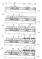
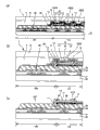


Classifications
-
- H—ELECTRICITY
- H05—ELECTRIC TECHNIQUES NOT OTHERWISE PROVIDED FOR
- H05B—ELECTRIC HEATING; ELECTRIC LIGHT SOURCES NOT OTHERWISE PROVIDED FOR; CIRCUIT ARRANGEMENTS FOR ELECTRIC LIGHT SOURCES, IN GENERAL
- H05B33/00—Electroluminescent light sources
- H05B33/12—Light sources with substantially two-dimensional [2D] radiating surfaces
- H05B33/22—Light sources with substantially two-dimensional [2D] radiating surfaces characterised by the chemical or physical composition or the arrangement of auxiliary dielectric or reflective layers
-
- H—ELECTRICITY
- H10—SEMICONDUCTOR DEVICES; ELECTRIC SOLID-STATE DEVICES NOT OTHERWISE PROVIDED FOR
- H10K—ORGANIC ELECTRIC SOLID-STATE DEVICES
- H10K59/00—Integrated devices, or assemblies of multiple devices, comprising at least one organic light-emitting element covered by group H10K50/00
- H10K59/10—OLED displays
- H10K59/12—Active-matrix OLED [AMOLED] displays
-
- H—ELECTRICITY
- H05—ELECTRIC TECHNIQUES NOT OTHERWISE PROVIDED FOR
- H05B—ELECTRIC HEATING; ELECTRIC LIGHT SOURCES NOT OTHERWISE PROVIDED FOR; CIRCUIT ARRANGEMENTS FOR ELECTRIC LIGHT SOURCES, IN GENERAL
- H05B33/00—Electroluminescent light sources
- H05B33/02—Details
-
- H—ELECTRICITY
- H10—SEMICONDUCTOR DEVICES; ELECTRIC SOLID-STATE DEVICES NOT OTHERWISE PROVIDED FOR
- H10K—ORGANIC ELECTRIC SOLID-STATE DEVICES
- H10K50/00—Organic light-emitting devices
- H10K50/80—Constructional details
- H10K50/85—Arrangements for extracting light from the devices
- H10K50/852—Arrangements for extracting light from the devices comprising a resonant cavity structure, e.g. Bragg reflector pair
-
- H—ELECTRICITY
- H10—SEMICONDUCTOR DEVICES; ELECTRIC SOLID-STATE DEVICES NOT OTHERWISE PROVIDED FOR
- H10K—ORGANIC ELECTRIC SOLID-STATE DEVICES
- H10K50/00—Organic light-emitting devices
- H10K50/80—Constructional details
- H10K50/85—Arrangements for extracting light from the devices
- H10K50/856—Arrangements for extracting light from the devices comprising reflective means
-
- H—ELECTRICITY
- H10—SEMICONDUCTOR DEVICES; ELECTRIC SOLID-STATE DEVICES NOT OTHERWISE PROVIDED FOR
- H10K—ORGANIC ELECTRIC SOLID-STATE DEVICES
- H10K59/00—Integrated devices, or assemblies of multiple devices, comprising at least one organic light-emitting element covered by group H10K50/00
- H10K59/80—Constructional details
- H10K59/875—Arrangements for extracting light from the devices
- H10K59/876—Arrangements for extracting light from the devices comprising a resonant cavity structure, e.g. Bragg reflector pair
-
- H—ELECTRICITY
- H10—SEMICONDUCTOR DEVICES; ELECTRIC SOLID-STATE DEVICES NOT OTHERWISE PROVIDED FOR
- H10K—ORGANIC ELECTRIC SOLID-STATE DEVICES
- H10K59/00—Integrated devices, or assemblies of multiple devices, comprising at least one organic light-emitting element covered by group H10K50/00
- H10K59/80—Constructional details
- H10K59/875—Arrangements for extracting light from the devices
- H10K59/878—Arrangements for extracting light from the devices comprising reflective means
-
- H—ELECTRICITY
- H10—SEMICONDUCTOR DEVICES; ELECTRIC SOLID-STATE DEVICES NOT OTHERWISE PROVIDED FOR
- H10K—ORGANIC ELECTRIC SOLID-STATE DEVICES
- H10K2102/00—Constructional details relating to the organic devices covered by this subclass
- H10K2102/301—Details of OLEDs
- H10K2102/302—Details of OLEDs of OLED structures
- H10K2102/3023—Direction of light emission
- H10K2102/3026—Top emission
-
- H—ELECTRICITY
- H10—SEMICONDUCTOR DEVICES; ELECTRIC SOLID-STATE DEVICES NOT OTHERWISE PROVIDED FOR
- H10K—ORGANIC ELECTRIC SOLID-STATE DEVICES
- H10K50/00—Organic light-emitting devices
- H10K50/80—Constructional details
- H10K50/805—Electrodes
- H10K50/81—Anodes
- H10K50/818—Reflective anodes, e.g. ITO combined with thick metallic layers
-
- H—ELECTRICITY
- H10—SEMICONDUCTOR DEVICES; ELECTRIC SOLID-STATE DEVICES NOT OTHERWISE PROVIDED FOR
- H10K—ORGANIC ELECTRIC SOLID-STATE DEVICES
- H10K50/00—Organic light-emitting devices
- H10K50/80—Constructional details
- H10K50/84—Passivation; Containers; Encapsulations
-
- H—ELECTRICITY
- H10—SEMICONDUCTOR DEVICES; ELECTRIC SOLID-STATE DEVICES NOT OTHERWISE PROVIDED FOR
- H10K—ORGANIC ELECTRIC SOLID-STATE DEVICES
- H10K50/00—Organic light-emitting devices
- H10K50/80—Constructional details
- H10K50/84—Passivation; Containers; Encapsulations
- H10K50/842—Containers
- H10K50/8426—Peripheral sealing arrangements, e.g. adhesives, sealants
-
- H—ELECTRICITY
- H10—SEMICONDUCTOR DEVICES; ELECTRIC SOLID-STATE DEVICES NOT OTHERWISE PROVIDED FOR
- H10K—ORGANIC ELECTRIC SOLID-STATE DEVICES
- H10K50/00—Organic light-emitting devices
- H10K50/80—Constructional details
- H10K50/84—Passivation; Containers; Encapsulations
- H10K50/844—Encapsulations
-
- H—ELECTRICITY
- H10—SEMICONDUCTOR DEVICES; ELECTRIC SOLID-STATE DEVICES NOT OTHERWISE PROVIDED FOR
- H10K—ORGANIC ELECTRIC SOLID-STATE DEVICES
- H10K59/00—Integrated devices, or assemblies of multiple devices, comprising at least one organic light-emitting element covered by group H10K50/00
- H10K59/80—Constructional details
- H10K59/87—Passivation; Containers; Encapsulations
-
- H—ELECTRICITY
- H10—SEMICONDUCTOR DEVICES; ELECTRIC SOLID-STATE DEVICES NOT OTHERWISE PROVIDED FOR
- H10K—ORGANIC ELECTRIC SOLID-STATE DEVICES
- H10K59/00—Integrated devices, or assemblies of multiple devices, comprising at least one organic light-emitting element covered by group H10K50/00
- H10K59/80—Constructional details
- H10K59/87—Passivation; Containers; Encapsulations
- H10K59/873—Encapsulations
Landscapes
- Engineering & Computer Science (AREA)
- Microelectronics & Electronic Packaging (AREA)
- Physics & Mathematics (AREA)
- Optics & Photonics (AREA)
- Electroluminescent Light Sources (AREA)
Applications Claiming Priority (3)
| Application Number | Priority Date | Filing Date | Title |
|---|---|---|---|
| JP2006068831A JP4809087B2 (ja) | 2006-03-14 | 2006-03-14 | エレクトロルミネッセンス装置、電子機器、およびエレクトロルミネッセンス装置の製造方法 |
| JP2006-068831 | 2006-03-14 | ||
| JP2006068831 | 2006-03-14 |
Publications (2)
| Publication Number | Publication Date |
|---|---|
| CN101038932A CN101038932A (zh) | 2007-09-19 |
| CN101038932B true CN101038932B (zh) | 2011-11-02 |
Family
ID=38038940
Family Applications (1)
| Application Number | Title | Priority Date | Filing Date |
|---|---|---|---|
| CN2007100885128A Expired - Fee Related CN101038932B (zh) | 2006-03-14 | 2007-03-14 | 电致发光装置、电子设备及电致发光装置的制造方法 |
Country Status (6)
| Country | Link |
|---|---|
| US (2) | US7796101B2 (de) |
| EP (1) | EP1835540A3 (de) |
| JP (1) | JP4809087B2 (de) |
| KR (1) | KR20070093830A (de) |
| CN (1) | CN101038932B (de) |
| TW (1) | TW200746897A (de) |
Cited By (1)
| Publication number | Priority date | Publication date | Assignee | Title |
|---|---|---|---|---|
| US9298057B2 (en) | 2012-07-20 | 2016-03-29 | Semiconductor Energy Laboratory Co., Ltd. | Display device and electronic device including the display device |
Families Citing this family (20)
| Publication number | Priority date | Publication date | Assignee | Title |
|---|---|---|---|---|
| JP5066836B2 (ja) * | 2005-08-11 | 2012-11-07 | セイコーエプソン株式会社 | 電気光学装置及び電子機器 |
| JP4809087B2 (ja) * | 2006-03-14 | 2011-11-02 | セイコーエプソン株式会社 | エレクトロルミネッセンス装置、電子機器、およびエレクトロルミネッセンス装置の製造方法 |
| KR20100071084A (ko) * | 2007-09-25 | 2010-06-28 | 이 아이 듀폰 디 네모아 앤드 캄파니 | 용액 처리된 전자 소자용 백플레인 구조물 |
| JP4816686B2 (ja) | 2008-06-06 | 2011-11-16 | ソニー株式会社 | 走査駆動回路 |
| KR101499235B1 (ko) | 2008-06-23 | 2015-03-06 | 삼성디스플레이 주식회사 | 유기 발광 표시 장치 및 그 제조 방법 |
| JP5040933B2 (ja) * | 2009-01-21 | 2012-10-03 | セイコーエプソン株式会社 | 有機el装置、有機el装置の製造方法、電子機器 |
| JP5182176B2 (ja) * | 2009-03-18 | 2013-04-10 | セイコーエプソン株式会社 | 表示装置および電子機器 |
| JP2011184738A (ja) * | 2010-03-09 | 2011-09-22 | Fujifilm Corp | ガスバリアフィルムの製造方法 |
| KR101223725B1 (ko) | 2011-01-10 | 2013-01-17 | 삼성디스플레이 주식회사 | 유기발광표시장치 및 그 제조방법 |
| US9153628B2 (en) | 2012-02-08 | 2015-10-06 | Joled Inc. | Display panel having an inter-layer insulation layer with planar and protruding regions |
| US9151061B2 (en) | 2012-10-05 | 2015-10-06 | Fiber Cement Foam Systems Insulation, LLC | Method and a device to attach building trims |
| CN103943785A (zh) * | 2013-06-18 | 2014-07-23 | 厦门天马微电子有限公司 | 光学调节膜及其制造方法 |
| JP2015204237A (ja) * | 2014-04-15 | 2015-11-16 | 株式会社ジャパンディスプレイ | 有機エレクトロルミネッセンス表示装置および有機エレクトロルミネッセンス表示装置の製造方法 |
| CN106816558B (zh) * | 2017-04-14 | 2019-09-03 | 京东方科技集团股份有限公司 | 顶发射有机电致发光显示面板、其制作方法及显示装置 |
| JP2020129617A (ja) * | 2019-02-08 | 2020-08-27 | 株式会社ジャパンディスプレイ | 半導体装置および半導体装置の製造方法 |
| CN110764326A (zh) * | 2019-10-14 | 2020-02-07 | 深圳市华星光电半导体显示技术有限公司 | 液晶显示面板及其制备方法 |
| KR102789961B1 (ko) * | 2019-12-31 | 2025-04-04 | 엘지디스플레이 주식회사 | 표시패널과 이를 이용한 표시장치 |
| WO2021184235A1 (zh) * | 2020-03-18 | 2021-09-23 | 京东方科技集团股份有限公司 | 一种阵列基板及其制备方法和显示面板 |
| KR20210137823A (ko) * | 2020-05-11 | 2021-11-18 | 엘지디스플레이 주식회사 | 표시 장치 |
| JP7693338B2 (ja) | 2021-03-09 | 2025-06-17 | JDI Design and Development 合同会社 | 表示装置 |
Citations (1)
| Publication number | Priority date | Publication date | Assignee | Title |
|---|---|---|---|---|
| US6992439B2 (en) * | 2001-02-22 | 2006-01-31 | Semiconductor Energy Laboratory Co., Ltd. | Display device with sealing structure for protecting organic light emitting element |
Family Cites Families (19)
| Publication number | Priority date | Publication date | Assignee | Title |
|---|---|---|---|---|
| TW493152B (en) * | 1999-12-24 | 2002-07-01 | Semiconductor Energy Lab | Electronic device |
| US7061451B2 (en) * | 2001-02-21 | 2006-06-13 | Semiconductor Energy Laboratory Co., Ltd, | Light emitting device and electronic device |
| JP2003114626A (ja) | 2001-06-18 | 2003-04-18 | Semiconductor Energy Lab Co Ltd | 発光装置及びその作製方法 |
| US7248235B2 (en) * | 2001-09-14 | 2007-07-24 | Sharp Kabushiki Kaisha | Display, method of manufacturing the same, and method of driving the same |
| JP4101511B2 (ja) * | 2001-12-27 | 2008-06-18 | 株式会社半導体エネルギー研究所 | 発光装置及びその作製方法 |
| JP3953320B2 (ja) * | 2001-12-28 | 2007-08-08 | 三洋電機株式会社 | 表示装置及びその製造方法 |
| US7148508B2 (en) | 2002-03-20 | 2006-12-12 | Seiko Epson Corporation | Wiring substrate, electronic device, electro-optical device, and electronic apparatus |
| JP4015045B2 (ja) | 2002-03-20 | 2007-11-28 | セイコーエプソン株式会社 | 配線基板、電子装置及び電子機器 |
| JP4531341B2 (ja) * | 2003-02-28 | 2010-08-25 | 株式会社半導体エネルギー研究所 | 発光装置および電子機器 |
| TWI363574B (en) * | 2003-04-07 | 2012-05-01 | Semiconductor Energy Lab | Electronic apparatus |
| JP2004335207A (ja) * | 2003-05-02 | 2004-11-25 | Fuji Electric Holdings Co Ltd | 有機el素子とその製造方法 |
| JP4608921B2 (ja) * | 2004-03-22 | 2011-01-12 | ソニー株式会社 | 表示装置の製造方法および表示装置 |
| US7423373B2 (en) * | 2004-03-26 | 2008-09-09 | Semiconductor Energy Laboratory Co., Ltd. | Light emitting device and manufacturing method thereof |
| WO2005109964A1 (ja) * | 2004-04-21 | 2005-11-17 | Idemitsu Kosan Co., Ltd. | 有機エレクトロルミネッセンス表示装置 |
| KR20050113045A (ko) * | 2004-05-28 | 2005-12-01 | 삼성에스디아이 주식회사 | 유기 전계 발광 표시 소자 및 그 제조방법 |
| US20060038752A1 (en) * | 2004-08-20 | 2006-02-23 | Eastman Kodak Company | Emission display |
| KR100579198B1 (ko) * | 2004-09-08 | 2006-05-11 | 삼성에스디아이 주식회사 | 유기 전계 발광 표시 소자 및 그 제조방법 |
| JP4582004B2 (ja) * | 2006-01-13 | 2010-11-17 | セイコーエプソン株式会社 | 発光装置および電子機器 |
| JP4809087B2 (ja) * | 2006-03-14 | 2011-11-02 | セイコーエプソン株式会社 | エレクトロルミネッセンス装置、電子機器、およびエレクトロルミネッセンス装置の製造方法 |
-
2006
- 2006-03-14 JP JP2006068831A patent/JP4809087B2/ja not_active Expired - Fee Related
-
2007
- 2007-01-29 US US11/668,129 patent/US7796101B2/en not_active Expired - Fee Related
- 2007-03-12 EP EP07005038A patent/EP1835540A3/de not_active Withdrawn
- 2007-03-12 KR KR1020070024019A patent/KR20070093830A/ko not_active Ceased
- 2007-03-13 TW TW096108620A patent/TW200746897A/zh unknown
- 2007-03-14 CN CN2007100885128A patent/CN101038932B/zh not_active Expired - Fee Related
-
2010
- 2010-08-05 US US12/850,727 patent/US8059067B2/en not_active Expired - Fee Related
Patent Citations (1)
| Publication number | Priority date | Publication date | Assignee | Title |
|---|---|---|---|---|
| US6992439B2 (en) * | 2001-02-22 | 2006-01-31 | Semiconductor Energy Laboratory Co., Ltd. | Display device with sealing structure for protecting organic light emitting element |
Cited By (1)
| Publication number | Priority date | Publication date | Assignee | Title |
|---|---|---|---|---|
| US9298057B2 (en) | 2012-07-20 | 2016-03-29 | Semiconductor Energy Laboratory Co., Ltd. | Display device and electronic device including the display device |
Also Published As
| Publication number | Publication date |
|---|---|
| US20080036705A1 (en) | 2008-02-14 |
| CN101038932A (zh) | 2007-09-19 |
| US8059067B2 (en) | 2011-11-15 |
| EP1835540A3 (de) | 2012-10-17 |
| TW200746897A (en) | 2007-12-16 |
| EP1835540A2 (de) | 2007-09-19 |
| KR20070093830A (ko) | 2007-09-19 |
| JP2007250244A (ja) | 2007-09-27 |
| JP4809087B2 (ja) | 2011-11-02 |
| US20100295831A1 (en) | 2010-11-25 |
| US7796101B2 (en) | 2010-09-14 |
Similar Documents
| Publication | Publication Date | Title |
|---|---|---|
| CN101038932B (zh) | 电致发光装置、电子设备及电致发光装置的制造方法 | |
| KR100838082B1 (ko) | 유기발광 표시장치 및 그 제조방법 | |
| KR101073552B1 (ko) | 유기 발광 표시 장치 및 그 제조 방법 | |
| CN102163613B (zh) | 显示装置和显示装置的制造方法 | |
| US11974467B2 (en) | Semiconductor device | |
| US8242692B2 (en) | Organic light emitting diode display and method for manufacturing the same | |
| JP6584099B2 (ja) | 表示装置およびその製造方法 | |
| US20050253508A1 (en) | Organic electroluminescent display element, display device having the same, and manufacturing method of the same | |
| JP4608921B2 (ja) | 表示装置の製造方法および表示装置 | |
| JP2018200787A (ja) | 表示装置 | |
| TW201839979A (zh) | 有機發光顯示裝置及其製造方法 | |
| KR20040103062A (ko) | 유기전계 발광표시장치 및 그의 제조방법 | |
| JP6223070B2 (ja) | 有機el表示装置及び有機el表示装置の製造方法 | |
| KR20190091395A (ko) | 유기 발광 표시 장치 | |
| KR20190043195A (ko) | 유기 발광 표시 장치 및 이의 제조 방법 | |
| JP2009283242A (ja) | 有機el表示装置 | |
| US12568733B2 (en) | Display device manufacturing method | |
| KR100552959B1 (ko) | 광차단막을 내포하는 기판과 그의 제조 방법 및 그를사용하는 평판 표시 장치 | |
| US20230284482A1 (en) | Display device and method for manufacturing display device | |
| US20230309350A1 (en) | Display device and manufacturing method of the same | |
| US20230269991A1 (en) | Display device | |
| JP2007041203A (ja) | ディスプレイパネル | |
| JP6818590B2 (ja) | 有機el表示装置、及び有機el表示装置の製造方法 | |
| KR20080000475A (ko) | 유기전계 발광 표시소자 및 그 제조방법 |
Legal Events
| Date | Code | Title | Description |
|---|---|---|---|
| C06 | Publication | ||
| PB01 | Publication | ||
| C10 | Entry into substantive examination | ||
| SE01 | Entry into force of request for substantive examination | ||
| C14 | Grant of patent or utility model | ||
| GR01 | Patent grant | ||
| CF01 | Termination of patent right due to non-payment of annual fee |
Granted publication date: 20111102 Termination date: 20160314 |
|
| CF01 | Termination of patent right due to non-payment of annual fee |