CN101299599B - Method, apparatus and system for acquiring calibration capacitance value of transconductance filter - Google Patents
Method, apparatus and system for acquiring calibration capacitance value of transconductance filter Download PDFInfo
- Publication number
- CN101299599B CN101299599B CN2008100288013A CN200810028801A CN101299599B CN 101299599 B CN101299599 B CN 101299599B CN 2008100288013 A CN2008100288013 A CN 2008100288013A CN 200810028801 A CN200810028801 A CN 200810028801A CN 101299599 B CN101299599 B CN 101299599B
- Authority
- CN
- China
- Prior art keywords
- unit
- voltage value
- value
- capacitance
- calibration
- Prior art date
- Legal status (The legal status is an assumption and is not a legal conclusion. Google has not performed a legal analysis and makes no representation as to the accuracy of the status listed.)
- Expired - Fee Related
Links
Images


Classifications
-
- H—ELECTRICITY
- H03—ELECTRONIC CIRCUITRY
- H03H—IMPEDANCE NETWORKS, e.g. RESONANT CIRCUITS; RESONATORS
- H03H11/00—Networks using active elements
- H03H11/02—Multiple-port networks
- H03H11/04—Frequency selective two-port networks
-
- H—ELECTRICITY
- H03—ELECTRONIC CIRCUITRY
- H03H—IMPEDANCE NETWORKS, e.g. RESONANT CIRCUITS; RESONATORS
- H03H11/00—Networks using active elements
- H03H11/02—Multiple-port networks
- H03H11/04—Frequency selective two-port networks
- H03H11/12—Frequency selective two-port networks using amplifiers with feedback
- H03H11/1291—Current or voltage controlled filters
Landscapes
- Networks Using Active Elements (AREA)
Abstract
The inventive embodiment discloses a method for obtaining the transconductance filter calibration capacitance, a device and a system, wherein the method includes generating the current for performing the integral process to the simulation capacitance in a prescribed time, which is used for simulating the capacitance designed to the transconductance filter with even capacitance array; comparing the integral voltage obtained by the integration to the capacitance with the set voltage, through adjusting the control code, successively approximating and looking for the integral voltage and the simulation capacitance equal to the voltage as the calibration capacitance. The inventive embodiment has the advantage of increasing the performance of the transconductance filter without affecting the performance of the transconductance filter.
Description
Technical Field
The embodiment of the invention relates to the technical field of mobile communication, in particular to a method, a device and a system for obtaining a calibration capacitance value of a transconductance filter.
Background
Transconductance-capacitance filters (Gm-C, Gm-C filters) are one of the most common filter structures, and are characterized by low power consumption and high bandwidth, and can be applied to various wireless or wired technical fields.
For the on-chip integrated filter, a most prominent disadvantage is that the integrated capacitance and the resistance have a great process dependency, which often causes a large deviation between the cut-off frequency of the filter and the design value, and affects the performance of the filter, so that a filter calibration circuit becomes indispensable along with the design of the on-chip integrated filter, and in the structure of the transconductance capacitance filter, in order to realize the frequency calibration of the filter (sometimes, the quality factor Q of the filter is also calibrated), the filter is generally realized by using a transconductance calibration (Gm tuning).
Due to the cut-off frequency of the filter Proportional, and therefore often by varying the transconductance (G) when performing filter frequency calibrationm) Of (c), two common types of GmThe cell, MOS transistor input (or bipolar transistor input) and degeneration resistance input stage are shown in fig. 1. The G ismA significant feature of the unit is GmThe magnitude of the value is not absolutely related to the current or resistance, so it is difficult to control the cut-off frequency of the filter with a discrete current, and thus calibration (tuning) of a digital Phase-Locked Loop (PLL) structure becomes very popular.
Filter frequency calibration using PLL for adjusting tail current as shown in fig. 2, a PLL is integrated on a chip, and the PLL uses an Oscillator (VCO) composed of Gm-C cells having the same structure as the filter to implement frequency Control, and determines the frequency Control of the Oscillator by adjusting the tail current of the VCO.
In the process of implementing the invention, the inventor finds that the existing filter frequency calibration technology has the following defects:
the frequency calibration by changing the tail current causes the linearity of the filter to change with the change of the tail current, thereby affecting the performance of the transconductance filter.
Disclosure of Invention
Embodiments of the present invention provide a method, an apparatus, and a system for obtaining a calibration capacitance value of a transconductance filter, which can improve accuracy of calibration of the transconductance filter without affecting performance of the transconductance filter.
To solve the above problem, an embodiment of the present invention provides a method for obtaining a calibration capacitance value of a transconductance filter, including:
generating a current to carry out integration processing on the analog capacitor within a specified time; the analog capacitor is used for simulating the capacitance of a transconductance filter which is arranged into a uniform capacitor array;
and comparing the integral voltage value obtained by integrating the capacitor array with a set voltage value, and gradually approaching and searching the value of the analog capacitor which enables the integral voltage value to be equal to the set voltage value through adjusting the control code to be used as a calibration capacitance value.
Correspondingly, an embodiment of the present invention further provides an apparatus for obtaining a calibration capacitance value of a transconductance filter, including:
the current supply unit is used for generating a current to charge the integrator unit;
an integrator unit for integrating an analog capacitor for simulating a transconductance filter capacitor set as a uniform capacitor array for a prescribed time in a case of charging;
the comparator unit is used for comparing an integral voltage value obtained by integrating the analog capacitor with a set voltage value;
and the controller unit is used for searching the value of the analog capacitor which enables the integral voltage value to be equal to the set voltage value through successive approximation by adjusting the control code to serve as the calibration capacitance value.
Accordingly, an embodiment of the present invention further provides a calibration system for a transconductance filter, including:
a device for obtaining a calibration capacitance value of a transconductance filter, configured to obtain an integral voltage value by integrating an analog capacitor, where the analog capacitor simulates a transconductance filter capacitor set as a uniform capacitor array, and searches for an analog capacitance value, which makes the integral voltage value equal to a set voltage value, as a calibration capacitance value by adjusting successive approximation of a control code, stores the control code corresponding to the calibration capacitance value, and provides the calibration capacitance value to the transconductance filter to calibrate the capacitance value of the transconductance filter;
and the transconductance filter is used for calibrating a capacitor part in the transconductance unit to be a calibration capacitance value corresponding to the control code according to the control code provided by the device for obtaining the calibration capacitance value of the transconductance filter.
The calibration mode provided by the embodiment of the invention is a linear discrete mode, the linearity of the transconductance filter cannot be changed along with the change of the tail current, and the performance of the transconductance filter is improved on the premise of not influencing the performance of the transconductance filter.
Drawings
Fig. 1 is a schematic diagram of two basic prior art transconductance units;
FIG. 2 is a schematic diagram of a prior art filter frequency calibration using a PLL to adjust the tail current;
fig. 3 is a schematic diagram of a calibration system for a transconductance filter according to an embodiment of the present invention;
fig. 4 is a schematic structural diagram of a first embodiment of an apparatus for obtaining a calibration capacitance value of a transconductance filter according to an embodiment of the present invention;
fig. 5 is a schematic structural diagram of an apparatus for obtaining a calibration capacitance value of a transconductance filter according to a second embodiment of the present invention;
fig. 6 is a schematic structural diagram of a controller unit in the apparatus for obtaining a calibration capacitance value of a transconductance filter according to an embodiment of the present invention;
FIG. 7 is a schematic diagram of a 5bit binary control code control calibration process;
fig. 8 is a schematic structural diagram of an integrator unit in the apparatus for obtaining calibration capacitance of a transconductance filter according to the embodiment of the present invention;
FIG. 9 is a schematic diagram of the operation of an integrator unit provided by an embodiment of the present invention;
FIG. 10 is a schematic diagram of an integrator unit auto-zero provided by an embodiment of the present invention;
FIG. 11 is a schematic diagram illustrating an embodiment of a voltage comparator unit for performing accurate voltage subtraction and amplifying;
FIG. 12 is a timing diagram illustrating the control of an apparatus for obtaining calibration capacitance of a transconductance filter according to an embodiment of the present invention;
fig. 13 is a schematic structural diagram of an apparatus for obtaining a calibration capacitance value of a transconductance filter according to a third embodiment of the present invention;
fig. 14 is a flowchart illustrating a first embodiment of a method for obtaining a calibration capacitance value of a transconductance filter according to an embodiment of the present invention;
fig. 15 is a flowchart illustrating a second embodiment of a method for obtaining a calibration capacitance value of a transconductance filter according to an embodiment of the present invention;
fig. 16 is a schematic flowchart of an integrated voltage value obtained by integrating the capacitor array within a predetermined time according to an embodiment of the present invention;
FIG. 17 is a schematic flow chart illustrating a method for finding a calibration capacitance value with an integrated voltage value equal to a predetermined voltage value according to a successive approximation method;
fig. 18 is a flowchart illustrating a third embodiment of a method for obtaining a calibration capacitance value of a transconductance filter according to an embodiment of the present invention.
Detailed Description
The embodiment of the invention provides a method for obtaining a calibration capacitance value of a transconductance filter and a device for obtaining the calibration capacitance value of the transconductance filter, which can improve the calibration accuracy of the transconductance filter on the premise of not influencing the performance of the transconductance filter.
Fig. 3 is a schematic diagram of a calibration system of a transconductance filter according to an embodiment of the present invention.
As shown in fig. 3, the filter calibration system includes:
the device 1 for obtaining the calibration capacitance value of the transconductance filter is used for integrating through an analog capacitor to obtain an integral voltage value, searching for a calibration capacitance value which enables the integral voltage value to be equal to a set voltage value through successive approximation by adjusting a control code, and calibrating the capacitance value of the transconductance filter by using the control code corresponding to the calibration capacitance value; note that the analog capacitance is a capacitance that simulates the transconductance filter 2 arranged as a uniform capacitor array.
And the transconductance filter 2 is used for calibrating a capacitor part in the transconductance unit to be a calibration capacitance value corresponding to the control code according to the control code provided by the device 1 for obtaining the calibration capacitance value of the transconductance filter. The capacitance of the transconductance filter 2 is preset to a uniform array of capacitors.
The calibration mode between the device 1 for obtaining the calibration capacitance value of the transconductance filter and the transconductance filter 2 is a master-slave mode, and the calibration mode is linear discrete capacitance approximation, so that the problem that the linearity of the transconductance filter changes along with tail current to influence the performance of the transconductance filter in the calibration process is avoided, and the calibration accuracy of the transconductance filter is finally improved.
Fig. 4 is a schematic structural diagram of a first embodiment of an apparatus for obtaining a calibration capacitance value of a transconductance filter according to an embodiment of the present invention.
The device for obtaining the calibration capacitance value of the transconductance filter provided by the embodiment of the invention comprises:
a current supply unit 10 for generating a current to charge the integrator unit 11;
an integrator unit 11 for integrating the analog capacitor for a predetermined time in the case of charging; the analog capacitor simulates a capacitance of a transconductance filter preset as a uniform capacitor array;
and a comparator unit 12, configured to compare the integrated voltage value obtained by integrating the analog capacitor with a set voltage value.
The controller unit 13 is configured to adjust the control code, and successively approximate and search a value of the analog capacitor, which makes the integrated voltage value equal to the set voltage value, as a calibration capacitance value;
it should be noted that the current supply unit 10 may be a transconductance unit, and the transconductance unit simulates a structure of a transconductance unit in the calibrated transconductance filter; the current supply unit 10 may also be a differential current source. In the following embodiments, embodiments in which the current supply unit is a transconductance unit and a differential current source will be described, respectively.
Referring to fig. 5, a schematic structural diagram of a second embodiment of the apparatus for obtaining a calibration capacitance value of a transconductance filter according to the embodiment of the present invention is shown.
In the apparatus for obtaining a calibration capacitance value of a transconductance filter according to the embodiment of the present invention, the current supply unit is a transconductance unit 10 when the apparatus is specifically implemented, the transconductance unit 10 is a transconductance unit simulating a transconductance filter to be calibrated with the same structure, and a capacitor of the transconductance filter preset as a uniform capacitor array is simulated by an analog capacitor 115 in the integrator unit 11, so as to avoid an influence of linearity of the transconductance unit of the transconductance filter on calibration accuracy.
It should be noted that, by means of calibrating the frequency cut-off of the transconductance filter through the capacitors, the capacitors of the transconductance filter are first set to some smaller uniform capacitor arrays. For example, a capacitance of 2pF is expressed as the sum of 20 capacitances of 100fF, and the capacitances are set to two parts, a fixed capacitance and a calibration capacitance, and the size of a capacitor array, according to the frequency deviation range caused by the process, where C ═ Cfix+CtuningWherein, CfixA fixed number of unit capacitors; ctuningIs a configurable unit capacitance. Calibrated frequency is represented by CfixAnd CtuningIs determined by the ratio of (a) to (b).
Then, the variable capacitor 115 in the integrator unit 11 is used to simulate the capacitor array of the transconductance filter, the current generated by the transconductance unit 10 is used to integrate the variable capacitor 115 within a predetermined time, and the integrated voltage value is compared with the set voltage value until the optimal simulated capacitance value of the simulated capacitor 115 (i.e., the variable capacitor 115) is found, so that when the integrated voltage value is equal to the set voltage value, the calibration is finished, and at this time, the value of the simulated capacitor is the calibration capacitance value. Specifically, as shown in fig. 5, the apparatus 1 for obtaining the calibration capacitance value of the transconductance filter includes:
a transconductance unit 10, a positive output terminal 100 of which is connected to a positive input terminal 110 of the integrator unit 11, a negative output terminal 101 of which is connected to a negative input terminal 111 of the integrator unit 11, and an input current for charging the integrator unit 11;
an integrator unit 11, connected to the positive output terminal 100 of the transconductance unit 10 through a positive input terminal 110 thereof, and a negative input terminal 111 of the integrator unit 11 is connected to the negative output terminal 101 of the transconductance unit 10, or the positive input terminal 110 is connected to the negative output terminal 101 of the transconductance unit 10, and the negative input terminal 111 of the integrator unit 11 is connected to the positive output terminal 100 of the transconductance unit 10;
whereas one output 112 of integrator unit 11 is connected to positive input 120 of comparator unit 12 and the other output 113 is connected to negative input 121 of comparator unit 12, said inputs 110 and 111 being further connected to respective variable capacitors 115, the output 1150 of variable capacitors 115 being connected to common mode reference level VCM; integrating the variable capacitor 115 by the operational amplifier 114 under the action of the control code of the controller unit 13 for a predetermined time to obtain an integrated voltage value;
the apparatus 1 for obtaining calibration capacitance value of transconductance filter shown in fig. 5 further comprises:
the comparator unit 12 comprises a comparator 123 and a voltage amplifier 124, wherein a positive input end 120 of the comparator unit 12 is connected with an output end 112 of the integrator unit 11, a negative input end 121 of the comparator unit 12 is connected with an output end 113 of the integrator unit 11, an output end 125 and an output end 126 of the comparator unit 12 are connected with the comparator 123, the voltage amplifier 124 realizes voltage amplification and subtraction through two-phase switched capacitors, and the comparator 123 is used for comparing an integrated voltage value obtained by integrating the integrator unit 11 with a set voltage value; the output 122 of the comparator unit 11 is connected to the input 130 of the controller unit 13 to output the comparison result to the controller unit 13;
the apparatus 1 for obtaining calibration capacitance value of transconductance filter shown in fig. 5 further comprises:
a controller unit 13 for providing a control code to said integrator unit 11 via its output 131, controlling said integrator unit 11 to integrate the variable capacitor 115,and gradually adjust the control code according to the comparison result of the comparator unit 12 to find out the capacitance value with the same integral voltage value as the set voltage value as the calibration capacitance value. It should be noted that, in the embodiment of the present invention, the control code output by the controller unit 13 may be Nbit binary control code, and the adjustment range is (0-2)N-1) configurable unit capacitances CtuningWherein N is a natural number. For example, 5-bit binary control code with the adjusting range of (0-31) configurable unit capacitors Ctuning。
Referring to fig. 6, the controller unit 13 includes:
a control code output subunit 130, configured to output a binary control code of Nbit to the integrator unit 11, where N is a natural number;
the controller adjusting subunit 131 is configured to change the binary control code gradually, so as to find out a value of the analog capacitor having an integral voltage value equal to the set voltage value as a calibration capacitance value.
In particular, integrator unit 11 is charged by transconductance unit 10, and integrator unit 11 obtains an integrated voltage value Wherein G ismIs the transconductance value, VrefIs a set voltage value, Δ t is a prescribed integration time, CintIs to calibrate the value of the analog capacitance actually used by the
 integrator unit 11 to obtain an integrated voltage value V under the control of the binary control code output from the control code output subunit 130 of the controller unit 13outThe integrated voltage value V is then compared by comparator unit 12outAnd a set voltage value VrefComparing and judging Until the
 comparator unit 12 compares the integrated voltage value V under the control of the controller unit 13outAnd a set voltage value VrefAre equal, i.e. When the size of (2) is equal to 1, C at that timeintIt is the calibration capacitance value.
Specifically, the controller unit 13 controls the capacitance value by the binary control code of Nbit as follows:
the controller adjusting subunit 131 of the controller unit 13 adjusts the binary control code so that the initial analog capacitance value of the analog capacitance simulation performed by the integrator unit 11 for integration is: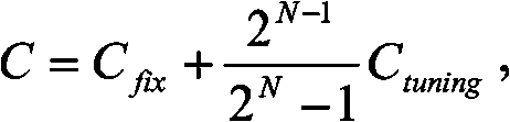
the initial analog capacitance value is measured And integrating to obtain an integral voltage value, and if the integral voltage value is greater than a set voltage value, changing the binary control code to ensure that the analog capacitance value is as follows:
if the integral voltage value is smaller than the set voltage value, the binary control code is changed, so that the analog capacitance value is as follows:
and repeating the steps, and gradually approaching and searching the value of the analog capacitor which enables the integral voltage value Vout to be equal to the set voltage value Vref by changing the binary control code, wherein the value of the analog capacitor is the calibration capacitance value.
The apparatus 1 for obtaining calibration capacitance of a transconductance filter shown in fig. 5 further comprises:
the detection unit 14 starts to search for the calibration capacitance value when detecting that the calibration control signal is valid;
and a memory unit 15, configured to store a control code corresponding to the calibration capacitance value when calibration is completed, and provide the control code to the transconductance filter to calibrate the capacitance value of the transconductance filter.
Referring to fig. 7, a schematic diagram of a 5-bit binary control code controlled calibration process is shown.
Taking a 5-bit binary control code as an example, first, the controller unit 13 automatically sets the 5-bit binary control code to 10000, and then the initial analog capacitance value of the analog capacitance simulation of the corresponding integrator integration is:
the initial analog capacitance value is measured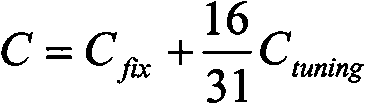 By the formula
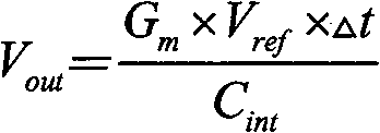 Integrating to obtain an integral voltage value, and if the integral voltage value V isoutGreater than a set voltage value VrefThen the
 controller unit 13 changes the binary control code to 11000, so that the analog capacitance value is: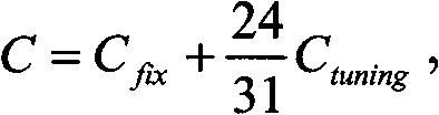
if the integral voltage value VoutLess than a set voltage value VrefThen the controller unit 13 changes the binary control code to 01000, so that the analog capacitance value is: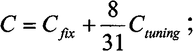
repeating the above steps, and changing the binary control code to search the integral voltage value V by successive approximationoutAnd a set voltage value VrefThe values of the analog capacitors, which are the calibration capacitance values, are equal. The binary control code determined finally is provided for the transconductance filter.
Since the input offset (offset) of the operational amplifier units 114(Op-amp) in the transconductance unit 10 and the integrator unit 11 affects the calibration accuracy, especially in the transconductance unit 10, during the integration process, the transconductance unit 10 needs to operate in a high linear region, the reference voltage of the input of the transconductance unit 10 cannot be very high, usually in tens of millivolts to hundreds of millivolts, because the direct current offset (DC offset) of the transconductance unit 10 of several millivolts or even more greatly affects the current output by the transconductance unit 10, thereby affecting the final output result of the integrator unit 11.
In order to solve the above problem, the integrator unit 11 provided with reference to the embodiment of the present invention, with reference to fig. 8, includes:
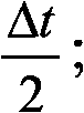
a time halving subunit 110 for dividing the integration time Δ t into two equal times
A first integrator unit 111 for integrating at a first one Within the integration time, carrying out forward integration on the analog capacitor to obtain a first integrated voltage value;
a second integrator sub-unit 112 for integrating at the second Within the integration time, performing reverse integration on the analog capacitor to obtain a second integration voltage value;
an integrated voltage value accumulating unit 113, configured to accumulate the first integrated voltage value and the second integrated voltage value to obtain a final integrated voltage value, so as to eliminate a dc offset generated by the transconductance unit or the differential current source.
The first integrator sub-unit 111 is at the first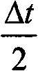 During the integration time, the analog capacitor is integrated in the forward direction, specifically, as shown in part (a) of fig. 9, a forward reference voltage V is first appliedrefInputting the voltage to the
 transconductance unit 10, connecting an anode output end 100 of the transconductance unit 10 with an anode input end 110 of the integrator unit 11, and connecting a cathode output end 101 of the transconductance unit 10 with a cathode input end 11 of the integrator unit 11 to obtain a first integral voltage value;

the integrated voltage value accumulation unit 113 is used for accumulating the first integrated voltage value and the second integrated voltage value to eliminate the DC offset generated by the transconductance unit 10 itself.
For the input DCoffset present in the operational amplifier unit 114(Op-amp) in the integrator unit 11, an embodiment of the present invention provides an auto-zero technique to eliminate the input DC offset present in the operational amplifier 114 (Op-amp).
As shown in fig. 10, the offset of Op-amp114 is eliminated by three periods of the discharging period (a), the self-calibration period (b), and the outputting period (c), so that the integrated voltage value of the final output is obtained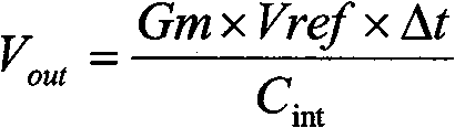 Heel G onlym、CintAnd Δ t.
In (a) a self-calibration period, the output terminals 1150 of the two variable capacitors 115 are respectively connected to the common-mode reference level VCM, the input terminal 110 and the output terminal 112 of the operational amplifier 114 are shorted, and the input terminal 111 and the output terminal 113 are shorted, so as to memorize the inherent DC offset of the operational amplifier 114 itself;
in the (b) charging period, the short-circuit switches of the input terminal 110 and the output terminal 112 of the operational amplifier 114 and the short-circuit switches of the input terminal 111 and the output terminal 113 are opened, the output terminals 1150 of the two variable capacitors 115 are respectively connected to the output terminal 112 and the output terminal 113 of the operational amplifier 114, and the transconductance unit 10 integrates the integrator unit 11 in the period;
in (c) output period: the input terminal 110 and the input terminal 111 of the operational amplifier 114 are short-circuited to output an integrated voltage.
For the voltage comparator 124 in the comparator unit 12, the embodiment of the present invention implements accurate voltage subtraction amplification by using a two-phase switched capacitor technology, as shown in fig. 11.
During (a) the self-calibration charging period, the input terminal 120 and the output terminal 125 of the voltage comparator 124 are shorted, the input terminal 121 and the output terminal 126 are shorted, and the input signal and the reference signal simultaneously charge the variable capacitor 115;
at (b) the input 120 and output 125 of the voltage comparator 124 are disconnected, the input 121 and output 126 are disconnected, and the charged variable capacitor 115 is disconnected from the common-mode level VCM, the output at this time being the comparison result.
Referring to fig. 12, a control timing diagram of an apparatus for obtaining a calibration capacitance value of a transconductance filter according to an embodiment of the present invention is shown.
When the detection module 14 of the apparatus 1 for obtaining the calibration capacitance value of the transconductance filter provided in the embodiment of the present invention detects that the calibration control signal is valid (RST) and the internal calibration valid signal (TUN _ enable) is at a low level, the calibration is started to set TUN _ enable to be valid, after the calibration is completed, the memory unit 15 updates the value of the originally stored control code and turns off the TUN _ enable signal.
The device for obtaining the calibration capacitance value of the transconductance filter, provided by the embodiment of the present invention, simulates the capacitance of the transconductance filter through the analog capacitor, the capacitance of the transconductance filter is preset to be a uniform capacitor array, the device for obtaining the calibration capacitance value of the transconductance filter also simulates the current generated by the transconductance unit of the transconductance filter, the integrated voltage value obtained by integrating the analog capacitor is compared with the set voltage value, successive approximation search is performed to obtain the calibration capacitance value which makes the integrated voltage value equal to the set voltage value, the calibration mode is a linear discrete mode, the linearity of the transconductance filter does not change with the change of the tail current, and the direct current offset generated by the transconductance unit is eliminated by performing forward integration and reverse integration on the capacitor array without affecting the performance of the transconductance filter, the performance of the transconductance filter is improved.
Referring to fig. 13, a schematic structural diagram of a third embodiment of the apparatus for obtaining a calibration capacitance value of a transconductance filter according to the embodiment of the present invention is shown.
The embodiment of the invention passes pair CintThe unit is properly converted to obtain a complete active R, C calibrationElectric circuit, in particular, CintThe structure of the apparatus 1 for obtaining the calibration capacitance of the transconductor filter is shown in fig. 13, and the apparatus is composed of a differential current output unit (or differential current source) 10, an integrator 11, a Comparator 12, a Control unit 14, a detection unit 14 and a memory unit 15, and the connection mode and the internal structure mode thereof are the same as those of the first embodiment, and are not described herein again. The current outputted by the differential current source 10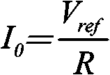 Is inversely proportional to the resistance R and is proportional to the set voltage value VrefIn direct proportion, the control method in the first embodiment of the present invention is utilized to integrate the capacitor array to obtain an integrated voltage value:
wherein, VrefIs a set voltage value, Δ t is a prescribed integration time, CintIs the capacitance value actually used for calibration. First, the voltage comparator 124 of the comparator unit 12 couples V by the two-phase switched capacitor techniqueoutThe voltages are subtracted and amplified, and then V is passed through the comparator 123 of the comparator unit 12outAnd VrefComparing, and searching the control code of the controller unit 13 to obtain the VoutAnd VrefEqual CintAnd the corresponding control code, at this time, CintI.e. the calibration capacitance value, the corresponding control code will be provided to the transconductance filter for use.
The device for obtaining the calibration capacitance value of the transconductance filter, provided by the embodiment of the present invention, simulates the capacitance of the transconductance filter through the analog capacitor, the capacitance of the transconductance filter is preset to be a uniform capacitor array, the device for obtaining the calibration capacitance value of the transconductance filter generates the current through the differential current source, the integrated voltage value obtained by integrating the capacitor array is compared with the set voltage value, the voltage value is compared with the set voltage value, and the calibration capacitance value which enables the integrated voltage value to be equal to the set voltage value is obtained by successive approximation and search, the calibration mode is a linear discrete mode, the linearity of the transconductance filter is not changed along with the change of the tail current, and the direct current offset generated by the transconductance unit is eliminated by performing forward integration and reverse integration on the capacitor array without affecting the performance of the transconductance filter, the performance of the transconductance filter is improved.
Referring to fig. 14, a flowchart of a first embodiment of a method for obtaining a calibration capacitance value of a transconductance filter according to an embodiment of the present invention is shown.
The method for obtaining the calibration capacitance value of the transconductance filter provided by the embodiment of the invention comprises the following steps:
firstly, in step 100, simulating the capacitance of the transconductance filter by using a simulation capacitor; the transconductance filter capacitors are preset into a uniform capacitor array;
in step 101, generating a current to perform an integration process on the analog capacitor within a specified time;
in step 102, comparing the integrated voltage value obtained by integrating the analog capacitor with a set voltage value; judging whether the integral voltage value is equal to the set voltage value or not; if not, the step 103 is executed; if yes, go to step 104;
in step 103, a calibration capacitance value which enables the integral voltage value to be equal to the set voltage value is searched by adjusting the control code successive approximation;
at step 104, a calibration capacitance value and a corresponding control code are obtained.
Referring to fig. 15, a flowchart of a method for obtaining a calibration capacitance value of a transconductance filter according to a second embodiment of the present invention is shown.
First, in step 200, the capacitance of a transconductance filter is modeled with an analog capacitance, the capacitance of the transconductance filter being preset to beA uniform capacitor array and arranged as both a fixed capacitor and a calibration capacitor, i.e. the capacitance size of the capacitor array, C ═ Cfix+CtuningWherein, CfixA fixed number of unit capacitors; ctuningIs a configurable unit capacitance. The calibration frequency range of the transconductance filter capacitor is CfixAnd CtuningThe ratio of (a) to (b) is determined.
In step 201, a transconductance unit of a transconductance filter is simulated to generate a current;
in step 202, the integrator is charged with the current, and the analog capacitor is integrated for a predetermined time to obtain an integrated voltage value:
wherein G ismIs the transconductance value, VrefIs a set voltage value, Δ t is a prescribed integration time, CintIs the value of the analog capacitance actually used for calibration. Said C isintControlled by binary code of Nbit, and the regulation range is (0-2)N-1) configurable unit capacitances CtuningWherein N is a natural number.
In step 202, an integrated voltage value V obtained by integrating the analog capacitor is obtainedoutAnd a set voltage value VrefComparing, and adjusting the control code to perform successive approximation search to obtain an integral voltage value VoutAnd a set voltage value VrefThe value of the equivalent analog capacitance serves as the calibration capacitance value. Specifically, by judging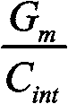 Whether the magnitude of (d) is equal to 1 or not, the integral voltage value V can be obtainedoutAnd a set voltage value VrefWhether or not they are equal, i.e.
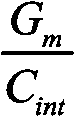 When the size of (2) is equal to 1, C at that timeintThen the calibration capacitance value is two corresponding to itThe binary control code is a binary control code obtained by calibration;
in step 203, the binary control code is saved and provided to the transconductance filter for use.
Specifically, referring to fig. 16, the step 201 of charging the integrator with the current and integrating the analog capacitor within a predetermined time to obtain an integrated voltage value specifically includes:
at step 2010, the integration time Δ t is divided into two equal times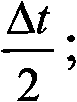
In step 2011, in the first one Within the integration time, carrying out forward integration on the analog capacitor to obtain a first integrated voltage value;
in step 2012, in the secondWithin the integration time, performing reverse integration on the analog capacitor to obtain a second integration voltage value;
in step 2013, the first and second integrated voltage values are added to obtain a final integrated voltage value, so as to eliminate the DC offset (DC offset) generated by the transconductance cell.
Fig. 17 is a schematic flow chart of a successive approximation method for finding a calibration capacitance value that makes the integrated voltage value equal to the set voltage value.
Step 202 of comparing the integrated voltage value obtained by integrating the analog capacitor with the set voltage value, and searching for a calibration capacitance value equal to the set voltage value by adjusting the control code successive approximation, includes:
at step 2020, the binary control code is adjusted such that the starting analog capacitance value of the analog capacitance simulation integrated by the integrator is: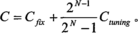
in step 2021, the starting analog capacitance value is determined By the formula
 Integrating to obtain an integral voltage value Vout;
in step 2022, the integral voltage value V is determinedoutWhether it is greater than the set voltage value Vref(ii) a If yes, go to step 2023, otherwise, go to step 2024;
in step 2023, the integrated voltage value VoutGreater than a set voltage value VrefThen, the binary control code is changed so that the analog capacitance value is:
in step 2024, the integrated voltage value VoutLess than a set voltage value VrefThen, the binary control code is changed so that the analog capacitance value is:
repeating the above steps, and changing the binary control code to search the integral voltage value V by successive approximationoutAnd a set voltage value VrefEqual values of analog capacitance Cint;
Finally, in step 2025, the value C of an analog capacitor is foundintSo that the integrated voltage value VrefAnd a set voltage value VrefEqual, the modeValue C of the pseudo-capacitanceintI.e. the calibration capacitance value; the binary control code corresponding to it will be provided to the transconductance filter for use.
In the method for obtaining a calibration capacitance value of a transconductance filter according to the embodiments of the present invention, a filter capacitor preset as a capacitor array is simulated by an analog capacitor, a current is generated by an analog transconductance unit, an integrated voltage value obtained by integrating the analog capacitor is compared with a set voltage value, and a value of the analog capacitor that makes the integrated voltage value equal to the set voltage value is obtained as the calibration capacitance value by successive approximation search.
Referring to fig. 18, a flowchart of a method for obtaining a calibration capacitance value of a transconductance filter according to a third embodiment of the present invention is shown.
First, in step 300, a capacitor is used to simulate the capacitance of the filter, the capacitance of the transconductance filter is preset to be a uniform capacitor array, and is set to be two parts of a fixed capacitor and a calibration capacitor, namely, the capacitance of the capacitor array, where C is equal to Cfix+Ctuning,
Wherein, CintA fixed number of unit capacitors; ctuningIs a configurable unit capacitance. The calibration frequency range of the transconductance filter capacitor is CintAnd CtuningThe ratio of (a) to (b) is determined.
In step 301, a current is generated by a differential current source;
in step 302, the integrator is charged with the current, and the analog capacitor is integrated for a predetermined time to obtain an integrated voltage value: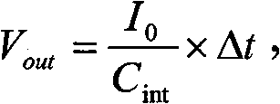
wherein,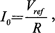 I0is the current value, V, generated by a differential current sourcerefIs a set voltage value, Δ t is a prescribed integration time, CintIs the value of the analog capacitance actually used for calibration. Said C isintControlled by binary code of Nbit, and the regulation range is (0-2)N-1) configurable unit capacitances CtuningWherein N is a natural number.
In step 303, an integral voltage value V obtained by integrating the analog capacitor is obtainedoutAnd a set voltage value VrefComparing, and adjusting the control code to perform successive approximation search to obtain an integral voltage value VoutAnd a set voltage value VrefThe value of the equivalent analog capacitance serves as the calibration capacitance value. Specifically, by judgingWhether the magnitude of (d) is equal to 1 or not, the integral voltage value V can be obtainedoutAnd a set voltage value VrefWhether or not they are equal, i.e. When the magnitude of (1) is equal to 1, the calibration is finished, and C is obtainedintIf the value is the calibration capacitance value, the binary control code corresponding to the calibration capacitance value is the binary control code obtained by calibration;
in step 304, the binary control code is saved and provided to the transconductance filter for use.
The method for obtaining the calibration capacitance value of the transconductance filter provided by the embodiment of the invention uses a capacitor to simulate the capacitor of the transconductance filter, generates current through a differential current source, integrates the analog capacitor to obtain an integral voltage value, compares the voltage value with a set voltage value, and successively approaches and searches to obtain the value of the analog capacitor which enables the integral voltage value to be equal to the set voltage value as the calibration capacitance value.
Through the above description of the embodiments, those skilled in the art will clearly understand that the present invention may be implemented by software plus a necessary hardware platform, and may also be implemented by hardware entirely. With this understanding in mind, all or part of the technical solutions of the present invention that contribute to the background can be embodied in the form of a software product, which can be stored in a storage medium, such as a ROM/RAM, a magnetic disk, an optical disk, etc., and includes instructions for causing a computer device (which can be a personal computer, a server, or a network device, etc.) to execute the methods according to the embodiments or some parts of the embodiments of the present invention.
While the invention has been described with reference to a preferred embodiment, it will be understood by those skilled in the art that various changes in form and details may be made therein without departing from the spirit and scope of the invention as defined by the appended claims.
Claims (22)


Priority Applications (3)
| Application Number | Priority Date | Filing Date | Title |
|---|---|---|---|
| CN2008100288013A CN101299599B (en) | 2008-06-16 | 2008-06-16 | Method, apparatus and system for acquiring calibration capacitance value of transconductance filter |
| PCT/CN2009/072224 WO2009152739A1 (en) | 2008-06-16 | 2009-06-11 | Method, apparatus and system for obtaining the transconductance filter calibration capacitance |
| US12/882,734 US8013670B2 (en) | 2008-06-16 | 2010-09-15 | Method, apparatus, and system for obtaining tuning capacitance for Gm-C filter |
Applications Claiming Priority (1)
| Application Number | Priority Date | Filing Date | Title |
|---|---|---|---|
| CN2008100288013A CN101299599B (en) | 2008-06-16 | 2008-06-16 | Method, apparatus and system for acquiring calibration capacitance value of transconductance filter |
Publications (2)
| Publication Number | Publication Date |
|---|---|
| CN101299599A CN101299599A (en) | 2008-11-05 |
| CN101299599B true CN101299599B (en) | 2011-12-28 |
Family
ID=40079307
Family Applications (1)
| Application Number | Title | Priority Date | Filing Date |
|---|---|---|---|
| CN2008100288013A Expired - Fee Related CN101299599B (en) | 2008-06-16 | 2008-06-16 | Method, apparatus and system for acquiring calibration capacitance value of transconductance filter |
Country Status (3)
| Country | Link |
|---|---|
| US (1) | US8013670B2 (en) |
| CN (1) | CN101299599B (en) |
| WO (1) | WO2009152739A1 (en) |
Families Citing this family (8)
| Publication number | Priority date | Publication date | Assignee | Title |
|---|---|---|---|---|
| CN101299599B (en) | 2008-06-16 | 2011-12-28 | 华为技术有限公司 | Method, apparatus and system for acquiring calibration capacitance value of transconductance filter |
| CN101825694B (en) * | 2010-04-01 | 2013-02-06 | 北京大学 | Offset capacitance automatic calibration circuit and method |
| CN101854151A (en) * | 2010-05-31 | 2010-10-06 | 广州市广晟微电子有限公司 | Frequency tuning method and system for transconductance-capacitance filter |
| CN103607209A (en) * | 2013-11-11 | 2014-02-26 | 清华大学 | DC imbalance calibration system and DC imbalance calibration method |
| CN105450222A (en) * | 2014-08-13 | 2016-03-30 | 南京能瑞自动化设备股份有限公司 | VCO swing automatic calibration circuit and method |
| CN109496273B (en) | 2018-01-24 | 2021-05-11 | 深圳市汇顶科技股份有限公司 | Capacitance detection circuit, touch detection device and terminal equipment |
| CN116264451A (en) * | 2021-12-15 | 2023-06-16 | 中芯国际集成电路制造(上海)有限公司 | How the autotune works |
| CN119892067B (en) * | 2025-01-09 | 2025-11-25 | 慷智集成电路(上海)有限公司 | Voltage-controlled oscillators, phase-locked loops, electronic equipment and vehicles |
Citations (1)
| Publication number | Priority date | Publication date | Assignee | Title |
|---|---|---|---|---|
| WO2007085997A1 (en) * | 2006-01-25 | 2007-08-02 | Nxp B.V. | Continuous-time sigma-delta analog-to-digital converter with capacitor and/or resistance digital self-calibration means for rc spread compensation |
Family Cites Families (9)
| Publication number | Priority date | Publication date | Assignee | Title |
|---|---|---|---|---|
| US6194947B1 (en) * | 1998-07-24 | 2001-02-27 | Global Communication Technology Inc. | VCO-mixer structure |
| KR100283619B1 (en) * | 1998-12-03 | 2001-03-02 | 정선종 | Frequency Tuning Circuit for Continuous-Time Filters |
| US6483380B1 (en) | 2000-09-18 | 2002-11-19 | Conexant Systems, Inc. | GMC filter and method for suppressing unwanted signals introduced by the filter |
| TW541788B (en) * | 2002-06-19 | 2003-07-11 | Ind Tech Res Inst | The frequency-tuning loop used in the transconductor-capacitor filter |
| US6903602B2 (en) * | 2003-09-08 | 2005-06-07 | Texas Instruments Incorporated | Calibrated fully differential RC filter |
| TWI283512B (en) * | 2004-07-08 | 2007-07-01 | Via Tech Inc | Transconductance filtering circuit |
| US7418213B2 (en) * | 2004-08-12 | 2008-08-26 | Finisar Corporation | Transimpedance amplifier with integrated filtering and reduced parasitic capacitance |
| TWI312231B (en) * | 2005-02-17 | 2009-07-11 | Via Tech Inc | Gm-c time constant tuning circuit |
| CN101299599B (en) * | 2008-06-16 | 2011-12-28 | 华为技术有限公司 | Method, apparatus and system for acquiring calibration capacitance value of transconductance filter |
-
2008
- 2008-06-16 CN CN2008100288013A patent/CN101299599B/en not_active Expired - Fee Related
-
2009
- 2009-06-11 WO PCT/CN2009/072224 patent/WO2009152739A1/en not_active Ceased
-
2010
- 2010-09-15 US US12/882,734 patent/US8013670B2/en active Active
Patent Citations (1)
| Publication number | Priority date | Publication date | Assignee | Title |
|---|---|---|---|---|
| WO2007085997A1 (en) * | 2006-01-25 | 2007-08-02 | Nxp B.V. | Continuous-time sigma-delta analog-to-digital converter with capacitor and/or resistance digital self-calibration means for rc spread compensation |
Also Published As
| Publication number | Publication date |
|---|---|
| US8013670B2 (en) | 2011-09-06 |
| WO2009152739A1 (en) | 2009-12-23 |
| CN101299599A (en) | 2008-11-05 |
| US20110050333A1 (en) | 2011-03-03 |
Similar Documents
| Publication | Publication Date | Title |
|---|---|---|
| CN101299599B (en) | Method, apparatus and system for acquiring calibration capacitance value of transconductance filter | |
| Mita et al. | Design guidelines for reversed nested Miller compensation in three-stage amplifiers | |
| KR100393303B1 (en) | Filter circuit | |
| US6737851B1 (en) | Calibration circuit | |
| CN108918980B (en) | A capacitance signal measurement circuit and measurement method | |
| KR100459714B1 (en) | DC offset compensation circuit and method of closed loop operational amplifier | |
| CN108023557B (en) | A Switched Capacitor Common Mode Feedback Structure | |
| Herencsar et al. | New compact VM four-phase oscillator employing only single z-copy VDTA and all grounded passive elements | |
| CN112422106B (en) | Comparator for inhibiting offset voltage and method for inhibiting offset voltage of comparator | |
| US20040041599A1 (en) | Non-linear reference waveform generators for data conversion and other applications | |
| CN108134592A (en) | The RC time constants calibration circuit and method of a kind of active filter | |
| CN110113028B (en) | Voltage divider and integral time constant calibration circuit of on-chip active RC filter | |
| CN103795371B (en) | Signal processing apparatus with low frequency compensating for frequency response circuit | |
| US7078960B2 (en) | Method and system for filter tuning using a digital trim value | |
| US20160042203A1 (en) | Charge measurement | |
| CN112881775B (en) | Low-power-consumption high-resolution capacitance measuring circuit | |
| CN101330284B (en) | Time constant correction device and related method | |
| CN111819790B (en) | Method for operating an optical sensor device with improved offset correction and optical sensor device | |
| CN117353744A (en) | Analog-to-digital conversion circuits and equipment | |
| CN113098402B (en) | Low-power-consumption band-pass amplifying circuit with self-calibration center frequency | |
| CN118138045A (en) | Offset calibration method and circuit for comparator array | |
| WO2014120457A1 (en) | Tuning circuitry and method for active filters | |
| JP2007251942A (en) | Calibration loop capable of automatically calibrating central frequency of filter, filter circuit and associated methods | |
| CN118939065B (en) | Bandgap reference circuit and bandgap reference voltage calibration method | |
| CN108886343B (en) | Negative feedback amplifying circuit |
Legal Events
| Date | Code | Title | Description |
|---|---|---|---|
| C06 | Publication | ||
| PB01 | Publication | ||
| C10 | Entry into substantive examination | ||
| SE01 | Entry into force of request for substantive examination | ||
| C14 | Grant of patent or utility model | ||
| GR01 | Patent grant | ||
| CF01 | Termination of patent right due to non-payment of annual fee |
Granted publication date: 20111228 |
|
| CF01 | Termination of patent right due to non-payment of annual fee |