CN101415519B - Laser processing method and processing apparatus based on conventional laser-induced material changes - Google Patents
Laser processing method and processing apparatus based on conventional laser-induced material changes Download PDFInfo
- Publication number
- CN101415519B CN101415519B CN2006800541650A CN200680054165A CN101415519B CN 101415519 B CN101415519 B CN 101415519B CN 2006800541650 A CN2006800541650 A CN 2006800541650A CN 200680054165 A CN200680054165 A CN 200680054165A CN 101415519 B CN101415519 B CN 101415519B
- Authority
- CN
- China
- Prior art keywords
- laser
- ultrafast
- pulse
- auxiliary
- induced material
- Prior art date
- Legal status (The legal status is an assumption and is not a legal conclusion. Google has not performed a legal analysis and makes no representation as to the accuracy of the status listed.)
- Expired - Fee Related
Links
Images


Classifications
-
- H—ELECTRICITY
- H01—ELECTRIC ELEMENTS
- H01S—DEVICES USING THE PROCESS OF LIGHT AMPLIFICATION BY STIMULATED EMISSION OF RADIATION [LASER] TO AMPLIFY OR GENERATE LIGHT; DEVICES USING STIMULATED EMISSION OF ELECTROMAGNETIC RADIATION IN WAVE RANGES OTHER THAN OPTICAL
- H01S3/00—Lasers, i.e. devices using stimulated emission of electromagnetic radiation in the infrared, visible or ultraviolet wave range
- H01S3/10—Controlling the intensity, frequency, phase, polarisation or direction of the emitted radiation, e.g. switching, gating, modulating or demodulating
-
- B—PERFORMING OPERATIONS; TRANSPORTING
- B23—MACHINE TOOLS; METAL-WORKING NOT OTHERWISE PROVIDED FOR
- B23K—SOLDERING OR UNSOLDERING; WELDING; CLADDING OR PLATING BY SOLDERING OR WELDING; CUTTING BY APPLYING HEAT LOCALLY, e.g. FLAME CUTTING; WORKING BY LASER BEAM
- B23K26/00—Working by laser beam, e.g. welding, cutting or boring
- B23K26/02—Positioning or observing the workpiece, e.g. with respect to the point of impact; Aligning, aiming or focusing the laser beam
- B23K26/06—Shaping the laser beam, e.g. by masks or multi-focusing
- B23K26/0604—Shaping the laser beam, e.g. by masks or multi-focusing by a combination of beams
- B23K26/0613—Shaping the laser beam, e.g. by masks or multi-focusing by a combination of beams having a common axis
-
- B—PERFORMING OPERATIONS; TRANSPORTING
- B23—MACHINE TOOLS; METAL-WORKING NOT OTHERWISE PROVIDED FOR
- B23K—SOLDERING OR UNSOLDERING; WELDING; CLADDING OR PLATING BY SOLDERING OR WELDING; CUTTING BY APPLYING HEAT LOCALLY, e.g. FLAME CUTTING; WORKING BY LASER BEAM
- B23K26/00—Working by laser beam, e.g. welding, cutting or boring
- B23K26/02—Positioning or observing the workpiece, e.g. with respect to the point of impact; Aligning, aiming or focusing the laser beam
- B23K26/06—Shaping the laser beam, e.g. by masks or multi-focusing
- B23K26/062—Shaping the laser beam, e.g. by masks or multi-focusing by direct control of the laser beam
- B23K26/0622—Shaping the laser beam, e.g. by masks or multi-focusing by direct control of the laser beam by shaping pulses
- B23K26/0624—Shaping the laser beam, e.g. by masks or multi-focusing by direct control of the laser beam by shaping pulses using ultrashort pulses, i.e. pulses of 1 ns or less
-
- B—PERFORMING OPERATIONS; TRANSPORTING
- B23—MACHINE TOOLS; METAL-WORKING NOT OTHERWISE PROVIDED FOR
- B23K—SOLDERING OR UNSOLDERING; WELDING; CLADDING OR PLATING BY SOLDERING OR WELDING; CUTTING BY APPLYING HEAT LOCALLY, e.g. FLAME CUTTING; WORKING BY LASER BEAM
- B23K26/00—Working by laser beam, e.g. welding, cutting or boring
- B23K26/34—Laser welding for purposes other than joining
-
- H—ELECTRICITY
- H01—ELECTRIC ELEMENTS
- H01S—DEVICES USING THE PROCESS OF LIGHT AMPLIFICATION BY STIMULATED EMISSION OF RADIATION [LASER] TO AMPLIFY OR GENERATE LIGHT; DEVICES USING STIMULATED EMISSION OF ELECTROMAGNETIC RADIATION IN WAVE RANGES OTHER THAN OPTICAL
- H01S3/00—Lasers, i.e. devices using stimulated emission of electromagnetic radiation in the infrared, visible or ultraviolet wave range
- H01S3/23—Arrangements of two or more lasers not provided for in groups H01S3/02 - H01S3/22, e.g. tandem arrangements of separate active media
- H01S3/2375—Hybrid lasers
Landscapes
- Physics & Mathematics (AREA)
- Optics & Photonics (AREA)
- Engineering & Computer Science (AREA)
- Plasma & Fusion (AREA)
- Mechanical Engineering (AREA)
- Electromagnetism (AREA)
- Laser Beam Processing (AREA)
- Lasers (AREA)
Abstract
本发明涉及一种显著地提高具有很高加工精度的常规超快激光微加工工艺的加工速度的技术。根据本发明,一种基于激光诱导材料瞬态变化的激光加工方法使超快激光的脉冲和至少一个与所述超快激光不同的辅助激光的脉冲耦合,以可逆地改变待加工材料。
This invention relates to a technique for significantly improving the processing speed of conventional ultrafast laser micromachining processes with high processing accuracy. According to the invention, a laser processing method based on laser-induced transient changes in materials couples an ultrafast laser pulse with at least one auxiliary laser pulse different from the ultrafast laser to reversibly alter the material to be processed.
Description
技术领域technical field
本发明涉及基于激光诱导材料状态瞬变的激光加工方法,该方法非线性地提高了具有非常高的加工精度的超快激光微加工工艺的加工速度。The invention relates to a laser processing method based on a laser-induced material state transient, which non-linearly increases the processing speed of an ultrafast laser micro-processing process with very high processing accuracy.
背景技术Background technique
随着电子和器件相关技术的发展,对于微加工工艺的需求日益增加。具体地说,由于大尺寸、小薄膜厚度、高集成度、高机械强度、高功能化组成材料和基板的多层涂覆结构的技术趋势,对于加工中封装和加工后封装的微加工技术的需要不断增加。这种加工技术要求约100微米的加工分辨率,因此通常使用金刚石锯切方法。然而,考虑到当前技术的发展趋势,由于机械和热损坏等的物理损坏,不能再使用金刚石锯切方法。由此,急需新的技术发展以克服诸如由于昂贵的金刚石锯片的磨损引起的成本增加的经济负担。为了克服传统的技术问题,最近提出了高功率的UV激光器。然而,由于对对象材料的冲击波和光化学损坏造成的机械损坏,高功率的UV激光器的使用存在局限性。然而,在生产下一代半导体材料和显示器件的加工工艺中,要求包括切割、钻孔、划线(scribing)和切片(dicing)的各种加工工艺的加工精度应达到数十微米而不造成对象材料的光电特性变化。With the development of electronics and device-related technologies, the demand for microfabrication processes is increasing. Specifically, due to the technical trend of large size, small film thickness, high integration, high mechanical strength, and multilayer coating structure of highly functionalized constituent materials and substrates, the micromachining technology for in-process encapsulation and post-process encapsulation The need is constantly increasing. This machining technique requires a machining resolution of about 100 microns, so diamond sawing is usually used. However, considering the current technological development trend, the diamond sawing method can no longer be used due to physical damage such as mechanical and thermal damage. Thus, new technological developments are urgently needed to overcome economic burdens such as increased costs due to wear of expensive diamond saw blades. To overcome conventional technical problems, high-power UV lasers have recently been proposed. However, there are limitations in the use of high-power UV lasers due to mechanical damage caused by shock waves and photochemical damage to the subject material. However, in the processing technology for producing next-generation semiconductor materials and display devices, it is required that the processing accuracy of various processing processes including dicing, drilling, scribing and dicing should reach tens of microns without causing objects. The optoelectronic properties of the material change.
已知情况是,超快激光技术可非常有效地应用于微加工,因为与利用相对较长激光脉冲的各种传统加工技术相比,它把热—机损坏减到最小。It is known that ultrafast laser technology can be very effectively applied to micromachining because it minimizes thermo-mechanical damage compared to conventional processing techniques using relatively long laser pulses.
此外,基于诸如电子束和等离子体的高能粒子的微加工会使元件的材料产生热损坏,并且根据材料的种类不能加工某些材料。因此,正在积极地进行超短脉冲激光加工技术的开发,以努力解决基于高能粒子的微加工的问题。In addition, micromachining based on high-energy particles such as electron beams and plasma causes thermal damage to materials of components, and some materials cannot be processed depending on the kind of materials. Therefore, the development of ultrashort pulse laser processing technology is being actively carried out in an effort to solve the problems of high-energy particle-based micromachining.
由于超快激光加工技术没有对于利用充足的激光功率提高加工速度不可缺少并很适用的放大技术,并且即使存在具有足够峰值功率的激光脉冲,也由于在加工过程之间在空气中的高阶非线性效应引起激光束特性的变化,无法提高加工速度。Since the ultrafast laser processing technology does not have the indispensable and suitable amplification technology to increase the processing speed with sufficient laser power, and even if there are laser pulses with sufficient peak power, due to the high-order nonlinearity in the air between processing processes The linear effect causes changes in the characteristics of the laser beam, which cannot increase the processing speed.
克服上述问题的新技术的前提条件是保持超快激光加工的特性而免受热和机械损坏。当前的基于超快激光的微加工工艺和加工技术就加工速度而言还很差,为了将该涉及未来的技术应用于产业,急需开发新的加工技术。为了克服基于超快激光的微加工工艺的局限性,需要采用了通常用于传统的相对长脉冲激光加工工艺的自适应光学系统的技术,因为原先的超快激光脉冲宽度和光束特性已经完全改变。当采用了自适应光学系统时,具体地说,由于脉冲宽度增大,在传统的相对长脉冲宽度的激光加工工艺中造成问题的热变形会降低加工质量。A prerequisite for new technologies to overcome the above-mentioned problems is to preserve the properties of ultrafast laser processing against thermal and mechanical damage. The current ultrafast laser-based micromachining process and processing technology are still poor in terms of processing speed, and in order to apply this future-related technology to industry, it is urgent to develop new processing technologies. In order to overcome the limitations of ultrafast laser-based micromachining processes, techniques using adaptive optics systems that are commonly used in conventional relatively long-pulse laser processing processes are required because the original ultrafast laser pulse width and beam characteristics have been completely changed. . When adaptive optics is employed, specifically, thermal distortion, which is problematic in conventional laser processing with relatively long pulse widths, degrades processing quality due to the increased pulse width.
发明内容Contents of the invention
技术问题technical problem
因此,开发了本发明以解决现有技术中出现的上述问题,并且本发明的主要目的是提供一种用于提高基于超快激光的微加工工艺的加工速度的基于激光诱导材料瞬态变化的激光加工方法和加工装置。Therefore, the present invention has been developed to solve the above-mentioned problems occurring in the prior art, and the main purpose of the present invention is to provide a laser-induced material transient change-based Laser processing method and processing device.
本发明的另一目的是提供一种基于激光诱导材料状态瞬态变化的激光加工方法和加工装置,其能够显著减小由大小为数十到数百纳米的微结构造成的表面粗糙度,该微结构形成在通过超快激光工艺加工的材料表面上,能够实现1微米级的加工,当对微光学器件施加所述超快激光加工工艺时产生该微结构。Another object of the present invention is to provide a laser processing method and processing device based on laser-induced transient changes in the state of materials, which can significantly reduce the surface roughness caused by microstructures with a size of tens to hundreds of nanometers, which A microstructure is formed on the surface of a material processed by an ultrafast laser process capable of processing on the order of 1 micron, which is produced when the ultrafast laser process is applied to a micro-optical device.
技术方案Technical solutions
为了实现本发明的目的,提供了一种基于激光诱导材料状态瞬态变化的激光加工方法,所述方法使超快激光的脉冲与不同于该超快激光的至少一个辅助激光的脉冲耦合,以可逆地改变待加工材料。In order to achieve the object of the present invention, a laser processing method based on a laser-induced transient state change of a material is provided, the method couples a pulse of an ultrafast laser with a pulse of at least one auxiliary laser different from the ultrafast laser, so as to Reversibly change the material to be processed.
所述超快激光器振荡出小于1皮秒的激光脉冲。The ultrafast laser oscillates laser pulses less than 1 picosecond.
所述辅助激光束的脉冲被控制为随时间变化。The pulse of the auxiliary laser beam is controlled to vary with time.
所述超快激光器的脉冲和所述至少一个辅助激光器的脉冲之间的耦合是控制所述超快激光脉冲和所述辅助激光脉冲之间的相对时间位置的时间耦合。The coupling between the pulses of the ultrafast laser and the pulses of the at least one auxiliary laser is a temporal coupling that controls the relative temporal position between the ultrafast laser pulses and the auxiliary laser pulses.
所述超快激光器的脉冲和所述至少一种辅助激光器的脉冲之间的耦合包括时间耦合和在空间上使所述超快激光束的焦点与所述辅助激光束的焦点一致的空间耦合。The coupling between the pulses of the ultrafast laser and the pulses of the at least one auxiliary laser includes a temporal coupling and a spatial coupling that spatially aligns the focus of the ultrafast laser beam with the focus of the auxiliary laser beam.
所述辅助激光束的脉冲宽度大于所述超快激光束的脉冲宽度。The pulse width of the auxiliary laser beam is greater than the pulse width of the ultrafast laser beam.
所述激光加工方法用于选自切割、钻孔、划线和切片的半导体加工工艺。The laser processing method is used in a semiconductor processing process selected from cutting, drilling, scribing and slicing.
为了实现本发明的目的,提供了一种基于激光诱导材料状态瞬态变化的激光加工装置,该装置包括:超快激光振荡器;辅助激光振荡器,该辅助激光振荡器包括随时间改变激光束脉冲的耦合电子装置;以及聚焦光学系统,该聚焦光学系统用于在空间上使所述超快激光振荡器生成的超快激光束的焦点与时间耦合的辅助激光束的焦点耦合,并使所述超快激光束和所述辅助激光束聚焦。In order to achieve the purpose of the present invention, a laser processing device based on laser-induced transient state change of materials is provided, the device includes: an ultrafast laser oscillator; an auxiliary laser oscillator, which includes a laser beam that changes with time pulsed coupling electronics; and a focusing optical system for spatially coupling the focal point of the ultrafast laser beam generated by the ultrafast laser oscillator with the focal point of the time-coupled auxiliary laser beam, and making the The ultrafast laser beam and the auxiliary laser beam are focused.
所述聚焦光学系统使所述辅助激光束聚焦在已聚焦的超快激光束之内。The focusing optics focus the auxiliary laser beam within the focused ultrafast laser beam.
所述聚焦光学系统使所述辅助激光束聚焦在已聚焦的超快激光束之外。The focusing optics focus the auxiliary laser beam out of the focused ultrafast laser beam.
基于激光诱导材料状态瞬态变化的激光加工装置还包括在所述超快激光振荡器和所述聚焦光学系统之间设置的偏振控制器,该偏振控制器用于利用步进电机控制半波长片的角度,以均匀地保持各个端口的透过偏振分束器的光功率。The laser processing device based on the transient change of the laser-induced material state also includes a polarization controller arranged between the ultrafast laser oscillator and the focusing optical system, and the polarization controller is used to control the movement of the half-wavelength plate by using a stepping motor Angle, in order to uniformly maintain the optical power of each port through the polarization beam splitter.
有益效果Beneficial effect
本发明提出了第一项超快激光加工技术,其中,通过常规的商用激光(如纳秒激光)与超快激光的时间-空间耦合,利用相对较少的超快激光能量局部并瞬时地改变待加工材料的物理状态(例如内部温度或载流子密度),并可逆地诱导物理状态的瞬态变化,从而能够显著地提高加工速度。更具体地,将诸如具有适当波长的纳秒激光的常规激光照射到待加工材料上,以瞬时地提高材料的内部温度或诸如自由电子的载流子的密度。在此,将激光的能量保持在使材料的状态可逆变化的程度,使得材料的状态没有实质的改变。这种材料状态改变使得能够通过同时照射到同一点上的超快激光来进行加工,在相同的能量状态下显著地提高加工速度。这里,优化辅助激光的波长和脉冲宽度,以考虑超快激光的脉冲烧蚀深度和加工速度而三维地优化材料物理变化(例如内部温度或载流子密度)的深度分布。为此,本发明使不同激光的脉冲在时间和空间上耦合。The present invention proposes the first ultrafast laser processing technology, in which relatively small amounts of ultrafast laser energy are used to locally and instantaneously change the The physical state of the material to be processed (such as internal temperature or carrier density), and reversibly induce transient changes in the physical state, which can significantly increase the processing speed. More specifically, conventional laser light such as nanosecond laser light having an appropriate wavelength is irradiated onto the material to be processed to instantaneously increase the internal temperature of the material or the density of carriers such as free electrons. Here, the energy of the laser light is maintained to such an extent that the state of the material is reversibly changed so that the state of the material is not substantially changed. This material state change enables processing by simultaneously irradiating ultrafast laser light on the same point, significantly increasing the processing speed at the same energy state. Here, the wavelength and pulse width of the auxiliary laser are optimized to three-dimensionally optimize the depth profile of material physical changes (such as internal temperature or carrier density) considering the pulse ablation depth and processing speed of the ultrafast laser. To this end, the invention couples pulses of different lasers temporally and spatially.
此外,本发明可利用耦合纳米激光来减少在超快激光加工中在材料表面上生成的大小为数十到数百微米的微结构的数量,以显著地降低材料的表面粗糙度。In addition, the present invention can use the coupled nano-laser to reduce the number of microstructures with a size of tens to hundreds of microns generated on the material surface during ultrafast laser processing, so as to significantly reduce the surface roughness of the material.
附图说明Description of drawings
根据随后的详细描述结合附图可更全面地理解本发明的其他目的和优点,图中:Other objects and advantages of the present invention can be more fully understood according to the ensuing detailed description in conjunction with the accompanying drawings, in which:
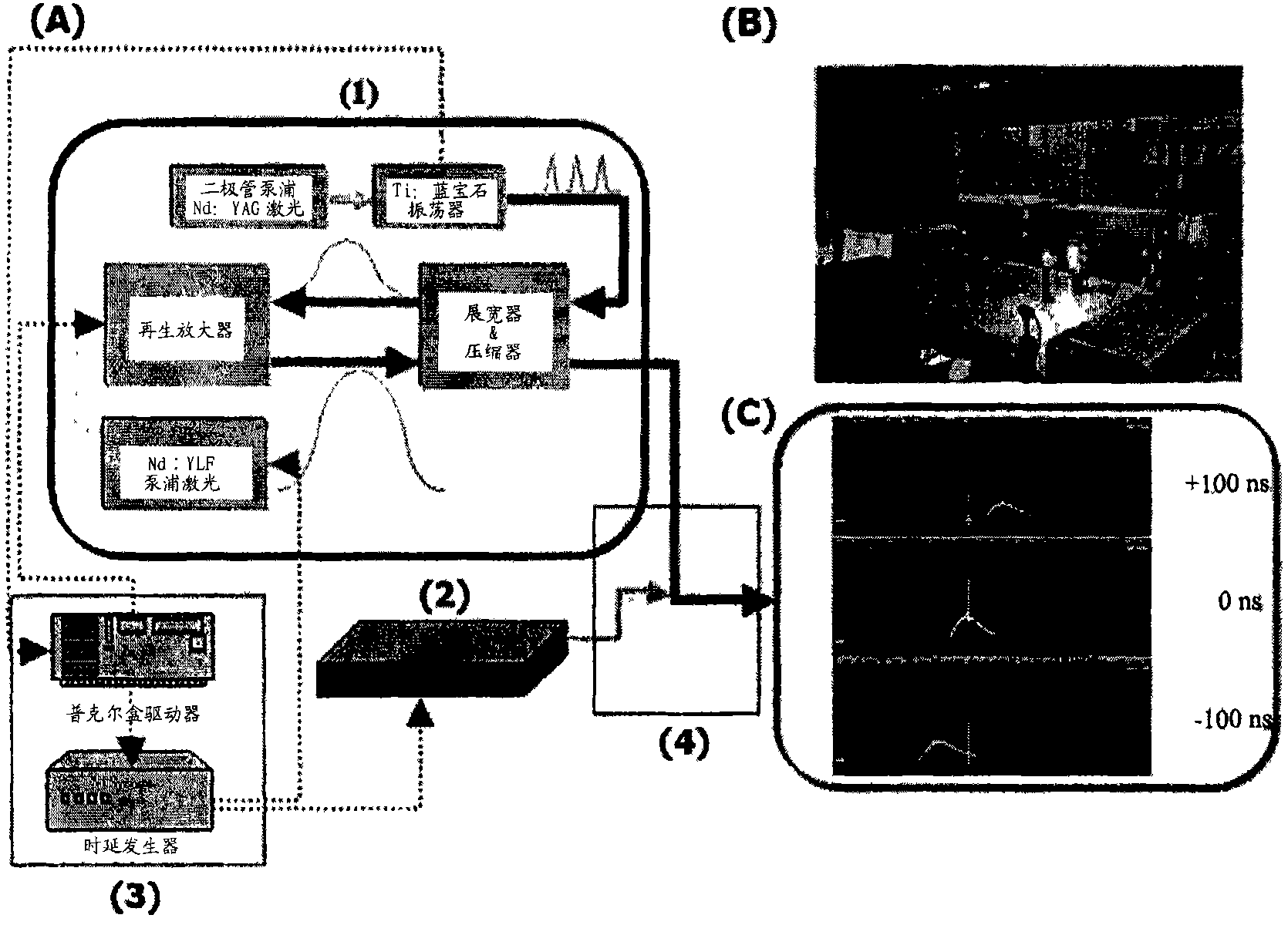
图1A例示了纳秒/超快激光混合加工工艺;Figure 1A illustrates a nanosecond/ultrafast laser hybrid processing process;
图1B是纳秒/超快激光混合加工装置的照片;Figure 1B is a photograph of a nanosecond/ultrafast laser hybrid processing device;
图1C示出了纳秒和超快激光脉冲之间三个不同时间-100ns、0ns和+100ns处的脉冲;Figure 1C shows pulses at three different times - 100 ns, 0 ns and +100 ns between nanosecond and ultrafast laser pulses;
图2例示了纳秒/超快激光混合加工工艺中待加工对象的温度以及载流子密度和光诱导反应的程度的变化;Fig. 2 exemplifies changes in the temperature of the object to be processed and the degree of carrier density and light-induced reaction in the nanosecond/ultrafast laser hybrid processing technology;
图3示出了硅划线加工工艺中纳秒激光和超快激光的脉冲的间隔;Fig. 3 shows the pulse interval of nanosecond laser and ultrafast laser in silicon scribing process;
图4是加工后的硅表面的原子力显微图片;Fig. 4 is the atomic force micrograph of the processed silicon surface;
图5是示出加工后的截面的曲线图;以及FIG. 5 is a graph showing a processed cross-section; and
图6是示出两种不同激光的间隔的变化和加工后的截面面积的的变化之间的关系图。FIG. 6 is a graph showing the relationship between the change in the interval of two different lasers and the change in the processed cross-sectional area.
附图标记的说明Explanation of reference signs
1:超快激光振荡器1: Ultrafast Laser Oscillator
2:辅助激光振荡器2: Auxiliary laser oscillator
3:耦合电子装置3: Coupling electronics
4:聚焦光学系统4: Focusing optical system
具体实施方案specific implementation plan
下面将参考附图结合优选实施方案详细描述本发明。Hereinafter, the present invention will be described in detail in conjunction with preferred embodiments with reference to the accompanying drawings.
图1A例示了纳秒/超快激光混合加工工艺,图1B是纳秒/超快激光混合加工装置的照片,图1C示出纳秒和超快激光脉冲之间在三个不同时间100ns、0ns和+100ns处的脉冲,图2例示了纳秒/超快激光混合加工工艺中待加工的对象的温度以及载流子密度和光诱导反应的程度的变化,以及图3是示出硅划线加工工艺中纳秒激光和超快激光的脉冲的间隔的图。图4是纳秒和超快激光脉冲之间的不同时间间隔下的加工后硅表面的原子力显微图片,图5是示出加工后的截面轮廓的图,以及图6是示出两种不同激光的间隔变化和加工后的截面面积的变化之间的关系图。参考图1,根据本发明的基于激光诱导材料状态瞬态变化的激光加工装置包括超快激光振荡器1,具有用于随时间改变激光束脉冲的耦合电子装置3的辅助激光振荡器2,以及用于将由超快激光振荡器1产生的超快激光束的焦点与时间耦合的辅助激光束的焦点在空间上耦合并使超快激光束和辅助激光束聚焦的聚焦光学系统4。Figure 1A illustrates the nanosecond/ultrafast laser hybrid processing process, Figure 1B is a photo of the nanosecond/ultrafast laser hybrid processing device, and Figure 1C shows three different times between nanosecond and ultrafast laser pulses 100ns, 0ns and Pulse at +100ns, Figure 2 illustrates the temperature of the object to be processed in the nanosecond/ultrafast laser hybrid processing process, as well as the change of the carrier density and the degree of light-induced reaction, and Figure 3 shows the silicon scribing process Diagram of the interval of the pulses of the nanosecond laser and the ultrafast laser. Figure 4 is an atomic force micrograph of a processed silicon surface at different time intervals between nanosecond and ultrafast laser pulses, Figure 5 is a graph showing the processed cross-sectional profile, and Figure 6 is a graph showing two different A graph showing the relationship between changes in laser spacing and changes in cross-sectional area after processing. Referring to FIG. 1 , a laser processing device based on a laser-induced transient change in the state of a material according to the present invention includes an
超快激光器1可使用飞秒激光器或皮秒激光器,而辅助激光器2可使用纳秒激光器。辅助激光束的脉冲宽度比超快激光器的脉冲宽度长。The
在本发明中,飞秒激光器用作超快激光器1,而纳秒激光振荡器用作辅助激光振荡器2。In the present invention, a femtosecond laser is used as the
飞秒激光和纳秒激光的时间耦合是指控制飞秒脉冲和纳秒脉冲的相对时间位置以在对材料进行激光加工时瞬态地改变材料的物理状态,而空间耦合是指飞秒激光束的焦点和纳秒激光束的焦点彼此一致。为了获得混合效应,同时要求时间耦合和空间耦合。飞秒激光器是Ti:蓝宝石放大器系统,其脉冲宽度为150fs,重复频率为1kHz,波长为800nm。纳秒激光器的脉冲宽度为250ns,重复频率为1kHz,波长为532nm。Temporal coupling of femtosecond and nanosecond lasers refers to controlling the relative time positions of femtosecond and nanosecond pulses to transiently change the physical state of materials when laser processing materials, while spatial coupling refers to the femtosecond laser beam The focal point of the nanosecond laser beam coincides with each other. In order to obtain the mixing effect, both temporal coupling and spatial coupling are required. The femtosecond laser is a Ti:sapphire amplifier system with a pulse width of 150 fs, a repetition rate of 1 kHz, and a wavelength of 800 nm. The pulse width of the nanosecond laser is 250ns, the repetition rate is 1kHz, and the wavelength is 532nm.
纳秒激光的稳定在混合激光加工系统的加工质量中起决定作用。本发明构建了纳秒激光的腔外稳定系统(extra-cavity stabilization system)。腔外稳定系统包括偏振分束器和半波长片,并利用步进电机控制半波长片的角度,以在监测最终输出级的测量值的同时接近预定功率值。结果,在通过有源稳定系统后约2%的长期稳定度变为小于0.5%,从而获得满意的稳定效果。可通过使用时延发生器并调节时延而使施加到飞秒激光器和纳秒激光器的电信号耦合,来控制飞秒脉冲和纳秒脉冲的时间耦合。图1B示出了如上构建的激光加工装置的照片。图1C示出了由上述方法控制的飞秒脉冲和纳秒脉冲之间的相对时间位置。通过使施加给飞秒激光的放大级所需的绿激光器的普克尔盒(pockels cell)的触发脉冲与纳秒激光器的触发脉冲耦合,可任意地对飞秒激光和纳秒激光的脉冲给定约-100ns到数十微秒的时间间隔。可以利用计算机进行控制以实现加工速度的优化。The stability of the nanosecond laser plays a decisive role in the processing quality of the hybrid laser processing system. The present invention constructs an extra-cavity stabilization system for nanosecond lasers. The extracavity stabilization system includes a polarizing beam splitter and a half-wavelength plate, and uses a stepper motor to control the angle of the half-wavelength plate to approach a predetermined power value while monitoring the measured value of the final output stage. As a result, the long-term stability of about 2% becomes less than 0.5% after passing through the active stabilization system, thereby obtaining a satisfactory stabilization effect. The temporal coupling of the femtosecond and nanosecond pulses can be controlled by using a time delay generator and adjusting the time delay to couple the electrical signals applied to the femtosecond and nanosecond lasers. Fig. 1B shows a photograph of the laser processing apparatus constructed as above. Figure 1C shows the relative temporal position between femtosecond and nanosecond pulses controlled by the method described above. The pulses of femtosecond laser and nanosecond laser can be arbitrarily given by coupling the trigger pulse of the green laser Pockels cell (pockels cell) required for the amplification stage of the femtosecond laser with the trigger pulse of the nanosecond laser. Contract time intervals from -100ns to tens of microseconds. Computer control can be used to optimize processing speed.
图2解释了当加工样品时,飞秒激光和纳秒激光的时间耦合造成样品的局部温度变化,以降低飞秒激光加工需要的烧蚀阈值能量,并提高加工速度。当提高纳秒激光器的功率时,加工材料的物理状态,例如材料温度或材料中的载流子密度会变化。在此,可以控制能量,使得纳秒激光不能单独诱发不可逆的变化。当耦合的飞秒激光脉冲被导入相同空间时,可用较少的能量进行对材料的大量不可逆烧蚀。因此,可以最大程度地提高飞秒激光加工的加工速度,并且加工阈值能量的降低能够显著地减小飞秒激光在空气中聚焦时伴随的高阶非线性以及由该高阶非线性导致的加工质量劣化。此外,当提高飞秒激光的重复频率的技术改善时,加工速度的提高可获得乘法效应,而不是加法效应。另外,通过优化纳秒激光的聚焦平面的适当空间变化和纳秒激光的脉冲宽度,可进一步提高加工速度。Figure 2 explains that when the sample is processed, the time coupling of the femtosecond laser and the nanosecond laser causes the local temperature change of the sample to reduce the ablation threshold energy required for femtosecond laser processing and increase the processing speed. When increasing the power of a nanosecond laser, the physical state of the processed material, such as the temperature of the material or the carrier density in the material, changes. Here, the energy can be controlled such that the nanosecond laser alone cannot induce irreversible changes. When coupled femtosecond laser pulses are directed into the same space, a large amount of irreversible ablation of the material can be performed with less energy. Therefore, the processing speed of femtosecond laser processing can be improved to the greatest extent, and the reduction of processing threshold energy can significantly reduce the high-order nonlinearity accompanying femtosecond laser focusing in air and the processing caused by this high-order nonlinearity. Deterioration of quality. Furthermore, as the technology to increase the repetition rate of femtosecond lasers improves, the increase in processing speed can have a multiplicative effect rather than an additive effect. In addition, the processing speed can be further increased by optimizing the appropriate spatial variation of the focal plane of the nanosecond laser and the pulse width of the nanosecond laser.
图2示出纳秒激光束聚焦在由聚焦光学系统聚焦的飞秒激光束之内。聚焦光学系统可以使纳秒激光束聚焦在已聚焦的飞秒激光束之外。这对于钻孔是非常有用的。Figure 2 shows that a nanosecond laser beam is focused within a femtosecond laser beam focused by a focusing optics system. Focusing optics can focus the nanosecond laser beam outside the focused femtosecond laser beam. This is very useful for drilling holes.
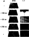
图3示出在混合加工中施加在硅晶片上的脉冲。在本发明中,给出了约800ns的脉冲间隔。利用AFM(原子力显微镜)对施加了激光脉冲的硅晶片的表面进行分析。图4示出了加工部分的测量曲线。参考图4,当纳秒激光和飞秒激光之间的时间间隔变为0时加工部分的变化最大。图5示出测量截面和纳秒激光与飞秒激光之间的时间间隔变化的关系。参考图5,对截面而言加工速度明显提高。图6示出烧蚀面积作为纳秒和飞秒激光脉冲之间的时间间隔(延迟时间)的函数。参考图6,对截面中的烧蚀面积而言加工速度提高了超过10倍。Figure 3 shows pulses applied to a silicon wafer during hybrid processing. In the present invention, a pulse interval of about 800 ns is given. The surface of the silicon wafer to which the laser pulse was applied was analyzed using an AFM (atomic force microscope). Figure 4 shows the measured curves of the machined part. Referring to FIG. 4, the variation of the processed portion is greatest when the time interval between the nanosecond laser and the femtosecond laser becomes 0. FIG. 5 shows the relationship between the measurement cross-section and the change in time interval between nanosecond laser light and femtosecond laser light. Referring to Fig. 5, the processing speed is significantly increased for the section. Figure 6 shows the ablated area as a function of the time interval (delay time) between nanosecond and femtosecond laser pulses. Referring to Figure 6, the processing speed was increased by more than 10 times for the ablated area in cross-section.
将对基板的纳秒激光诱导物理变化对飞秒激光加工工艺的影响的评估和优化加工条件的技术开发的研究应用于硅晶片划线加工中。由于在包括封装工艺的各种工艺中使硅晶片变薄的处理的加速,对于新的下一代加工技术的需求有所增加。因为诸如金刚石锯切的机械加工工艺造成机械损坏并且由于金刚石锯的磨损造成加工成本增加,对非常薄且硬的晶片很难直接应用常规的机械锯切方法,因此急需新的加工技术。因此,本发明提出的技术是非常有意义的。The research on the evaluation of the influence of nanosecond laser-induced physical changes of the substrate on the femtosecond laser processing process and the technical development of optimizing processing conditions is applied to the silicon wafer scribing process. Due to the acceleration of processes for thinning silicon wafers in various processes including packaging processes, demands for new next-generation processing technologies have increased. It is difficult to directly apply conventional mechanical sawing methods to very thin and hard wafers because of mechanical damage caused by mechanical processing processes such as diamond sawing and increased processing costs due to wear of diamond saws, thus new processing technologies are urgently needed. Therefore, the technology proposed by the present invention is very meaningful.
因此,在加工速度上本发明克服了加工技术的局限性,这种局限性是具有高加工精度的传统超快激光微加工工艺的缺点。要求提高加工速度,同时保持飞秒激光加工特性而免受由于飞秒激光放大技术的技术局限性和聚焦过程中的高阶非线性效应引起的热损坏和机械损坏。本发明是能够利用相对少的超快激光能量通过在时间—空间上使常规的商用激光(例如纳秒激光和飞秒激光)耦合并局部瞬时地改变加工材料的物理状态(例如内部温度),显著地提高加工速度的第一项超快激光加工技术。更具体地说,将诸如具有适当波长的纳秒激光的常规激光照射到加工材料上以瞬时地提高材料的内部温度或诸如自由电子的载流子密度。在此,诱导激光的能量保持在使材料的状态可逆地改变的程度,使得材料的状态没有实质性的改变。这种状态改变明显地改善了利用以相同能量照射到同一点的超快激光的加工工艺。优化诱导激光的波长和脉冲宽度,以便考虑超快激光脉冲的烧蚀深度和加工速度三维地优化物理变化(例如材料的内部温度)的深度分布。为了实现此构想,本发明使不同激光的脉冲在时间上或空间上进行耦合。Therefore, in terms of processing speed, the present invention overcomes the limitation of processing technology, which is the shortcoming of traditional ultrafast laser micromachining technology with high processing precision. It is required to increase the processing speed while maintaining femtosecond laser processing characteristics without thermal and mechanical damage due to technical limitations of femtosecond laser amplification technology and high-order nonlinear effects in the focusing process. The present invention is able to use relatively little ultrafast laser energy to couple conventional commercial lasers (such as nanosecond lasers and femtosecond lasers) in time-space and locally and instantaneously change the physical state of the processed material (such as internal temperature), The first ultrafast laser processing technology that significantly increases processing speed. More specifically, conventional laser light such as nanosecond laser light having an appropriate wavelength is irradiated onto the processed material to instantaneously increase the internal temperature of the material or the carrier density such as free electrons. Here, the energy of the induction laser is kept at such a level that the state of the material is reversibly changed so that the state of the material is not substantially changed. This state change significantly improves processing using ultrafast lasers hitting the same spot with the same energy. The wavelength and pulse width of the induction laser are optimized in order to three-dimensionally optimize the depth profile of physical changes such as the internal temperature of the material taking into account the ablation depth and processing speed of the ultrafast laser pulse. In order to realize this idea, the present invention couples the pulses of different lasers temporally or spatially.
工业实用性Industrial Applicability
如上所述,本发明可利用相对少的超快激光能量通过在时间—空间上使常规的商用激光(例如纳秒激光和飞秒激光)耦合并局部瞬时地改变加工材料的物理状态(例如内部温度或载流子密度),克服了常规超快激光微加工工艺的加工速度的局限性,从而显著地提高加工速度。因此,本发明有助于超快激光微加工工艺的工业化。具体地说,本发明使得能够进行不能应用常规加工技术的下一代半导体和显示器加工工艺中必需的多种加工工艺,包括切割、钻孔、划线和切块。此外,本发明可将加工精度提高到数十微米而不造成加工材料的光—电特性的改变。As described above, the present invention can utilize relatively little ultrafast laser energy to locally and instantaneously change the physical state of the processed material (such as internal temperature or carrier density), which overcomes the limitations of the processing speed of the conventional ultrafast laser micromachining process, thereby significantly increasing the processing speed. Therefore, the present invention contributes to the industrialization of the ultrafast laser micromachining process. Specifically, the present invention enables a variety of processing processes, including dicing, drilling, scribing, and dicing, necessary in next-generation semiconductor and display processing where conventional processing techniques cannot be applied. In addition, the present invention can increase the processing accuracy to tens of microns without causing changes in the photo-electric properties of the processed material.
尽管参考具体的示例性实施方式描述了本发明,但本发明不限于这些实施方式而由所附权利要求限定。可理解的是本领域技术人员可在不脱离本发明的范围和精神的情况下改变或修改实施方式。Although the present invention has been described with reference to specific exemplary embodiments, the invention is not limited to these embodiments but only by the appended claims. It is understood that those skilled in the art may change or modify the embodiments without departing from the scope and spirit of the present invention.
Claims (9)
Applications Claiming Priority (4)
| Application Number | Priority Date | Filing Date | Title |
|---|---|---|---|
| KR1020060020143A KR100795526B1 (en) | 2006-03-02 | 2006-03-02 | Laser processing method and processing equipment by causing material state variation |
| KR10-2006-0020143 | 2006-03-02 | ||
| KR1020060020143 | 2006-03-02 | ||
| PCT/KR2006/003051 WO2007100176A1 (en) | 2006-03-02 | 2006-08-03 | Laser processing method and processing apparatus based on conventional laser-induced material changes |
Publications (2)
| Publication Number | Publication Date |
|---|---|
| CN101415519A CN101415519A (en) | 2009-04-22 |
| CN101415519B true CN101415519B (en) | 2011-09-14 |
Family
ID=38459256
Family Applications (1)
| Application Number | Title | Priority Date | Filing Date |
|---|---|---|---|
| CN2006800541650A Expired - Fee Related CN101415519B (en) | 2006-03-02 | 2006-08-03 | Laser processing method and processing apparatus based on conventional laser-induced material changes |
Country Status (7)
| Country | Link |
|---|---|
| US (1) | US20100032416A1 (en) |
| EP (1) | EP1989017A4 (en) |
| JP (1) | JP2009528170A (en) |
| KR (1) | KR100795526B1 (en) |
| CN (1) | CN101415519B (en) |
| RU (1) | RU2401185C2 (en) |
| WO (1) | WO2007100176A1 (en) |
Families Citing this family (17)
| Publication number | Priority date | Publication date | Assignee | Title |
|---|---|---|---|---|
| US8232687B2 (en) | 2006-04-26 | 2012-07-31 | Raydiance, Inc. | Intelligent laser interlock system |
| US9130344B2 (en) | 2006-01-23 | 2015-09-08 | Raydiance, Inc. | Automated laser tuning |
| CN101909808B (en) * | 2008-01-17 | 2014-04-30 | 本田技研工业株式会社 | Laser processing device and laser processing method |
| KR101064352B1 (en) * | 2008-11-27 | 2011-09-14 | 한국표준과학연구원 | Ultrafast laser process speed and process section control method and control device using photo-induced transient absorption |
| CN102741010A (en) * | 2010-02-05 | 2012-10-17 | 株式会社藤仓 | Surface microstructure formation method and substrate having surface microstructure |
| US9120181B2 (en) | 2010-09-16 | 2015-09-01 | Coherent, Inc. | Singulation of layered materials using selectively variable laser output |
| JP5862088B2 (en) * | 2011-07-22 | 2016-02-16 | アイシン精機株式会社 | Laser cleaving method and laser cleaving apparatus |
| US10239160B2 (en) * | 2011-09-21 | 2019-03-26 | Coherent, Inc. | Systems and processes that singulate materials |
| CN102580786A (en) * | 2012-01-18 | 2012-07-18 | 华南理工大学 | Micro-channel sheet used as catalytic reaction carrier, and manufacturing method thereof |
| US9919380B2 (en) | 2013-02-23 | 2018-03-20 | Coherent, Inc. | Shaping of brittle materials with controlled surface and bulk properties |
| KR101483759B1 (en) * | 2013-07-19 | 2015-01-19 | 에이피시스템 주식회사 | Apparatus for processing fragile substrate using multi lasers and method thereof |
| WO2015108991A2 (en) * | 2014-01-17 | 2015-07-23 | Imra America, Inc. | Laser-based modification of transparent materials |
| EP2944413A1 (en) * | 2014-05-12 | 2015-11-18 | Boegli-Gravures S.A. | Device for mask projection of femtosecond and picosecond laser beams with a blade, a mask and lenses' systems |
| JP5841225B1 (en) * | 2014-12-12 | 2016-01-13 | 株式会社ブリヂストン | tire |
| JP2018523291A (en) * | 2015-06-01 | 2018-08-16 | エバナ テクノロジーズ ユーエービー | Method for scribing semiconductor workpiece |
| TWI677395B (en) * | 2018-03-31 | 2019-11-21 | 財團法人工業技術研究院 | Separating brittle material method and device thereof |
| CN109514076B (en) * | 2018-12-18 | 2020-04-14 | 北京工业大学 | A process method for picosecond-nanosecond laser composite asynchronous polishing of ceramics |
Citations (3)
| Publication number | Priority date | Publication date | Assignee | Title |
|---|---|---|---|---|
| DE3203287A1 (en) * | 1981-02-02 | 1982-08-19 | Olympus Optical Co., Ltd., Tokyo | Laser meter |
| US4707584A (en) * | 1985-12-12 | 1987-11-17 | Mitsubishi Denki Kabushiki Kaisha | Dual-polarization, dual-frequency cutting machine |
| CN1617783A (en) * | 2001-12-04 | 2005-05-18 | 通用原子公司 | Method and apparatus for increasing the material removal rate in laser machining |
Family Cites Families (8)
| Publication number | Priority date | Publication date | Assignee | Title |
|---|---|---|---|---|
| RU2116180C1 (en) * | 1997-05-26 | 1998-07-27 | Акционерное общество закрытого типа "Технолазер" | Optical focusing head for laser treatment |
| JP3982136B2 (en) * | 2000-02-04 | 2007-09-26 | セイコーエプソン株式会社 | Laser processing method and apparatus |
| DE10006516C2 (en) * | 2000-02-15 | 2002-01-10 | Datacard Corp | Process for processing workpieces using multiple laser beams |
| US7027155B2 (en) * | 2001-03-29 | 2006-04-11 | Gsi Lumonics Corporation | Methods and systems for precisely relatively positioning a waist of a pulsed laser beam and method and system for controlling energy delivered to a target structure |
| CA2436227A1 (en) * | 2001-12-17 | 2003-06-26 | Electro Scientific Industries, Inc. | Processing a memory link with a set of at least two laser pulses |
| JP4209615B2 (en) * | 2001-12-28 | 2009-01-14 | 株式会社ニデック | Laser processing equipment |
| JP2005305470A (en) * | 2004-04-19 | 2005-11-04 | Hikari Physics Kenkyusho:Kk | Ultraviolet-assisted ultrashort pulse laser processing apparatus and method |
| US8148211B2 (en) * | 2004-06-18 | 2012-04-03 | Electro Scientific Industries, Inc. | Semiconductor structure processing using multiple laser beam spots spaced on-axis delivered simultaneously |
-
2006
- 2006-03-02 KR KR1020060020143A patent/KR100795526B1/en not_active Expired - Lifetime
- 2006-08-03 JP JP2008557197A patent/JP2009528170A/en active Pending
- 2006-08-03 WO PCT/KR2006/003051 patent/WO2007100176A1/en not_active Ceased
- 2006-08-03 US US12/281,385 patent/US20100032416A1/en not_active Abandoned
- 2006-08-03 RU RU2008138865/02A patent/RU2401185C2/en not_active IP Right Cessation
- 2006-08-03 CN CN2006800541650A patent/CN101415519B/en not_active Expired - Fee Related
- 2006-08-03 EP EP06783504A patent/EP1989017A4/en not_active Withdrawn
Patent Citations (3)
| Publication number | Priority date | Publication date | Assignee | Title |
|---|---|---|---|---|
| DE3203287A1 (en) * | 1981-02-02 | 1982-08-19 | Olympus Optical Co., Ltd., Tokyo | Laser meter |
| US4707584A (en) * | 1985-12-12 | 1987-11-17 | Mitsubishi Denki Kabushiki Kaisha | Dual-polarization, dual-frequency cutting machine |
| CN1617783A (en) * | 2001-12-04 | 2005-05-18 | 通用原子公司 | Method and apparatus for increasing the material removal rate in laser machining |
Also Published As
| Publication number | Publication date |
|---|---|
| EP1989017A4 (en) | 2012-08-15 |
| KR20070090434A (en) | 2007-09-06 |
| RU2401185C2 (en) | 2010-10-10 |
| JP2009528170A (en) | 2009-08-06 |
| US20100032416A1 (en) | 2010-02-11 |
| EP1989017A1 (en) | 2008-11-12 |
| WO2007100176A1 (en) | 2007-09-07 |
| CN101415519A (en) | 2009-04-22 |
| KR100795526B1 (en) | 2008-01-16 |
| RU2008138865A (en) | 2010-04-10 |
Similar Documents
| Publication | Publication Date | Title |
|---|---|---|
| CN101415519B (en) | Laser processing method and processing apparatus based on conventional laser-induced material changes | |
| JP6563166B2 (en) | Dual laser beam system for use with FIB and / or electron microscope | |
| JP5496657B2 (en) | Laser machining of workpieces containing low dielectric materials | |
| CN104339088B (en) | For executing the system of laser filament in transparent material | |
| JP4418282B2 (en) | Laser processing method | |
| JP5380986B2 (en) | Laser scribing method and laser scribing apparatus | |
| JP4490883B2 (en) | Laser processing apparatus and laser processing method | |
| CN103477427A (en) | Methods and systems for laser processing a workpiece using a plurality of tailored laser pulse shapes | |
| KR101181719B1 (en) | Substrate Dicing Method by Nano Void Array Formation using Femtosecond Pulse Lasers | |
| WO2003049155A1 (en) | System and method for laser micro- machining | |
| JP2011519175A (en) | Semiconductor wafer dicing | |
| JP4607537B2 (en) | Laser processing method | |
| Jiao et al. | Picosecond laser drilling of silicon with applied voltage | |
| JP2005095952A (en) | Method and apparatus for dividing thin plate workpiece | |
| JP2005101413A (en) | Method and apparatus for dividing thin plate workpiece | |
| Kim et al. | Precision microfabrication of AlN and Al2O3 ceramics by femtosecond laser ablation | |
| Patel et al. | High speed micromachining with high power UV laser | |
| Qiao | Laser annealing on wafer | |
| Mingareev et al. | Laser Dicing of Silicon and Electronics Substrates | |
| Cai et al. | Damage‐Free Full‐Thickness Dicing of Ultra‐Thin GaAs Wafers Using a Femtosecond Laser with Low Residual Stress | |
| CN120862129A (en) | Sapphire laser hidden cutting method and system based on femtosecond laser-induced micro-holes | |
| Tamhankar et al. | Efficient use of short pulse width laser for maximum material removal rate | |
| Alexander et al. | Femtosecond laser drilling of high-aspect-ratio 1-micron holes in silicon | |
| JP2014097508A (en) | Laser processing method and method of manufacturing electronic device | |
| QI et al. | 1207 Mid-ultraviolet pulsed solid-state laser micromachining of SiC single crystal wafer |
Legal Events
| Date | Code | Title | Description |
|---|---|---|---|
| C06 | Publication | ||
| PB01 | Publication | ||
| C10 | Entry into substantive examination | ||
| SE01 | Entry into force of request for substantive examination | ||
| C14 | Grant of patent or utility model | ||
| GR01 | Patent grant | ||
| C17 | Cessation of patent right | ||
| CF01 | Termination of patent right due to non-payment of annual fee |
Granted publication date: 20110914 Termination date: 20130803 |