CN101794792A - Semiconductor device and manufacturing method thereof - Google Patents
Semiconductor device and manufacturing method thereof Download PDFInfo
- Publication number
- CN101794792A CN101794792A CN201010106921.8A CN201010106921A CN101794792A CN 101794792 A CN101794792 A CN 101794792A CN 201010106921 A CN201010106921 A CN 201010106921A CN 101794792 A CN101794792 A CN 101794792A
- Authority
- CN
- China
- Prior art keywords
- film
- semiconductor device
- gate electrode
- layer
- insulating film
- Prior art date
- Legal status (The legal status is an assumption and is not a legal conclusion. Google has not performed a legal analysis and makes no representation as to the accuracy of the status listed.)
- Pending
Links
Images






Classifications
-
- H—ELECTRICITY
- H10—SEMICONDUCTOR DEVICES; ELECTRIC SOLID-STATE DEVICES NOT OTHERWISE PROVIDED FOR
- H10B—ELECTRONIC MEMORY DEVICES
- H10B53/00—Ferroelectric RAM [FeRAM] devices comprising ferroelectric memory capacitors
- H10B53/30—Ferroelectric RAM [FeRAM] devices comprising ferroelectric memory capacitors characterised by the memory core region
-
- H—ELECTRICITY
- H10—SEMICONDUCTOR DEVICES; ELECTRIC SOLID-STATE DEVICES NOT OTHERWISE PROVIDED FOR
- H10B—ELECTRONIC MEMORY DEVICES
- H10B61/00—Magnetic memory devices, e.g. magnetoresistive RAM [MRAM] devices
- H10B61/20—Magnetic memory devices, e.g. magnetoresistive RAM [MRAM] devices comprising components having three or more electrodes, e.g. transistors
- H10B61/22—Magnetic memory devices, e.g. magnetoresistive RAM [MRAM] devices comprising components having three or more electrodes, e.g. transistors of the field-effect transistor [FET] type
-
- H—ELECTRICITY
- H10—SEMICONDUCTOR DEVICES; ELECTRIC SOLID-STATE DEVICES NOT OTHERWISE PROVIDED FOR
- H10B—ELECTRONIC MEMORY DEVICES
- H10B63/00—Resistance change memory devices, e.g. resistive RAM [ReRAM] devices
- H10B63/30—Resistance change memory devices, e.g. resistive RAM [ReRAM] devices comprising selection components having three or more electrodes, e.g. transistors
-
- H—ELECTRICITY
- H10—SEMICONDUCTOR DEVICES; ELECTRIC SOLID-STATE DEVICES NOT OTHERWISE PROVIDED FOR
- H10D—INORGANIC ELECTRIC SEMICONDUCTOR DEVICES
- H10D86/00—Integrated devices formed in or on insulating or conducting substrates, e.g. formed in silicon-on-insulator [SOI] substrates or on stainless steel or glass substrates
- H10D86/201—Integrated devices formed in or on insulating or conducting substrates, e.g. formed in silicon-on-insulator [SOI] substrates or on stainless steel or glass substrates the substrates comprising an insulating layer on a semiconductor body, e.g. SOI
-
- H—ELECTRICITY
- H10—SEMICONDUCTOR DEVICES; ELECTRIC SOLID-STATE DEVICES NOT OTHERWISE PROVIDED FOR
- H10W—GENERIC PACKAGES, INTERCONNECTIONS, CONNECTORS OR OTHER CONSTRUCTIONAL DETAILS OF DEVICES COVERED BY CLASS H10
- H10W15/00—Highly-doped buried regions of integrated devices
-
- H—ELECTRICITY
- H10—SEMICONDUCTOR DEVICES; ELECTRIC SOLID-STATE DEVICES NOT OTHERWISE PROVIDED FOR
- H10W—GENERIC PACKAGES, INTERCONNECTIONS, CONNECTORS OR OTHER CONSTRUCTIONAL DETAILS OF DEVICES COVERED BY CLASS H10
- H10W15/00—Highly-doped buried regions of integrated devices
- H10W15/01—Manufacture or treatment
-
- H—ELECTRICITY
- H10—SEMICONDUCTOR DEVICES; ELECTRIC SOLID-STATE DEVICES NOT OTHERWISE PROVIDED FOR
- H10W—GENERIC PACKAGES, INTERCONNECTIONS, CONNECTORS OR OTHER CONSTRUCTIONAL DETAILS OF DEVICES COVERED BY CLASS H10
- H10W20/00—Interconnections in chips, wafers or substrates
- H10W20/01—Manufacture or treatment
- H10W20/031—Manufacture or treatment of conductive parts of the interconnections
- H10W20/0698—Local interconnections
-
- H—ELECTRICITY
- H10—SEMICONDUCTOR DEVICES; ELECTRIC SOLID-STATE DEVICES NOT OTHERWISE PROVIDED FOR
- H10W—GENERIC PACKAGES, INTERCONNECTIONS, CONNECTORS OR OTHER CONSTRUCTIONAL DETAILS OF DEVICES COVERED BY CLASS H10
- H10W20/00—Interconnections in chips, wafers or substrates
- H10W20/20—Interconnections within wafers or substrates, e.g. through-silicon vias [TSV]
-
- H—ELECTRICITY
- H10—SEMICONDUCTOR DEVICES; ELECTRIC SOLID-STATE DEVICES NOT OTHERWISE PROVIDED FOR
- H10W—GENERIC PACKAGES, INTERCONNECTIONS, CONNECTORS OR OTHER CONSTRUCTIONAL DETAILS OF DEVICES COVERED BY CLASS H10
- H10W20/00—Interconnections in chips, wafers or substrates
- H10W20/20—Interconnections within wafers or substrates, e.g. through-silicon vias [TSV]
- H10W20/211—Through-semiconductor vias, e.g. TSVs
- H10W20/218—Through-semiconductor vias, e.g. TSVs in silicon-on-insulator [SOI] wafers
-
- H—ELECTRICITY
- H10—SEMICONDUCTOR DEVICES; ELECTRIC SOLID-STATE DEVICES NOT OTHERWISE PROVIDED FOR
- H10W—GENERIC PACKAGES, INTERCONNECTIONS, CONNECTORS OR OTHER CONSTRUCTIONAL DETAILS OF DEVICES COVERED BY CLASS H10
- H10W20/00—Interconnections in chips, wafers or substrates
- H10W20/40—Interconnections external to wafers or substrates, e.g. back-end-of-line [BEOL] metallisations or vias connecting to gate electrodes
- H10W20/481—Interconnections external to wafers or substrates, e.g. back-end-of-line [BEOL] metallisations or vias connecting to gate electrodes on the rear surfaces of the wafers or substrates
-
- H—ELECTRICITY
- H10—SEMICONDUCTOR DEVICES; ELECTRIC SOLID-STATE DEVICES NOT OTHERWISE PROVIDED FOR
- H10D—INORGANIC ELECTRIC SEMICONDUCTOR DEVICES
- H10D84/00—Integrated devices formed in or on semiconductor substrates that comprise only semiconducting layers, e.g. on Si wafers or on GaAs-on-Si wafers
- H10D84/01—Manufacture or treatment
- H10D84/0123—Integrating together multiple components covered by H10D12/00 or H10D30/00, e.g. integrating multiple IGBTs
- H10D84/0126—Integrating together multiple components covered by H10D12/00 or H10D30/00, e.g. integrating multiple IGBTs the components including insulated gates, e.g. IGFETs
- H10D84/0165—Integrating together multiple components covered by H10D12/00 or H10D30/00, e.g. integrating multiple IGBTs the components including insulated gates, e.g. IGFETs the components including complementary IGFETs, e.g. CMOS devices
- H10D84/017—Manufacturing their source or drain regions, e.g. silicided source or drain regions
-
- H—ELECTRICITY
- H10—SEMICONDUCTOR DEVICES; ELECTRIC SOLID-STATE DEVICES NOT OTHERWISE PROVIDED FOR
- H10D—INORGANIC ELECTRIC SEMICONDUCTOR DEVICES
- H10D84/00—Integrated devices formed in or on semiconductor substrates that comprise only semiconducting layers, e.g. on Si wafers or on GaAs-on-Si wafers
- H10D84/01—Manufacture or treatment
- H10D84/02—Manufacture or treatment characterised by using material-based technologies
- H10D84/03—Manufacture or treatment characterised by using material-based technologies using Group IV technology, e.g. silicon technology or silicon-carbide [SiC] technology
- H10D84/038—Manufacture or treatment characterised by using material-based technologies using Group IV technology, e.g. silicon technology or silicon-carbide [SiC] technology using silicon technology, e.g. SiGe
-
- H—ELECTRICITY
- H10—SEMICONDUCTOR DEVICES; ELECTRIC SOLID-STATE DEVICES NOT OTHERWISE PROVIDED FOR
- H10N—ELECTRIC SOLID-STATE DEVICES NOT OTHERWISE PROVIDED FOR
- H10N70/00—Solid-state devices having no potential barriers, and specially adapted for rectifying, amplifying, oscillating or switching
- H10N70/20—Multistable switching devices, e.g. memristors
- H10N70/24—Multistable switching devices, e.g. memristors based on migration or redistribution of ionic species, e.g. anions, vacancies
- H10N70/245—Multistable switching devices, e.g. memristors based on migration or redistribution of ionic species, e.g. anions, vacancies the species being metal cations, e.g. programmable metallization cells
-
- H—ELECTRICITY
- H10—SEMICONDUCTOR DEVICES; ELECTRIC SOLID-STATE DEVICES NOT OTHERWISE PROVIDED FOR
- H10N—ELECTRIC SOLID-STATE DEVICES NOT OTHERWISE PROVIDED FOR
- H10N70/00—Solid-state devices having no potential barriers, and specially adapted for rectifying, amplifying, oscillating or switching
- H10N70/801—Constructional details of multistable switching devices
- H10N70/821—Device geometry
- H10N70/826—Device geometry adapted for essentially vertical current flow, e.g. sandwich or pillar type devices
-
- H—ELECTRICITY
- H10—SEMICONDUCTOR DEVICES; ELECTRIC SOLID-STATE DEVICES NOT OTHERWISE PROVIDED FOR
- H10N—ELECTRIC SOLID-STATE DEVICES NOT OTHERWISE PROVIDED FOR
- H10N70/00—Solid-state devices having no potential barriers, and specially adapted for rectifying, amplifying, oscillating or switching
- H10N70/801—Constructional details of multistable switching devices
- H10N70/881—Switching materials
- H10N70/883—Oxides or nitrides
- H10N70/8833—Binary metal oxides, e.g. TaOx
Landscapes
- Internal Circuitry In Semiconductor Integrated Circuit Devices (AREA)
- Semiconductor Memories (AREA)
- Electrodes Of Semiconductors (AREA)
- Mram Or Spin Memory Techniques (AREA)
- Metal-Oxide And Bipolar Metal-Oxide Semiconductor Integrated Circuits (AREA)
- Hall/Mr Elements (AREA)
- Thin Film Transistor (AREA)
Abstract
本发明提供一种半导体器件及其制造方法。该半导体器件包括:扩散层,形成在基板的前表面处;低阻抗部,形成在扩散层的前表面处,并具有低于扩散层的阻抗;以及后接触电极,从基板的后表面贯穿基板以穿过扩散层连接到低阻抗部。

The invention provides a semiconductor device and a manufacturing method thereof. The semiconductor device includes: a diffusion layer formed at the front surface of the substrate; a low-resistance portion formed at the front surface of the diffusion layer and having an impedance lower than that of the diffusion layer; and a rear contact electrode penetrating the substrate from the rear surface of the substrate To connect to the low impedance part through the diffusion layer.
Description
技术领域technical field
本发明涉及一种半导体器件及其制造方法。The invention relates to a semiconductor device and a manufacturing method thereof.
背景技术Background technique
接触电极与栅极电极之间的距离根据缩放比例(scaling)减小,且栅极电极与接触电极之间的寄生电容的显著增加引起栅极电极的寄生电容的显著增加,并且引起电路运行速度的劣化和负载电容的增加,这导致功耗的增加。The distance between the contact electrode and the gate electrode decreases according to scaling, and a significant increase in the parasitic capacitance between the gate electrode and the contact electrode causes a significant increase in the parasitic capacitance of the gate electrode, and causes a circuit operating speed degradation and an increase in load capacitance, which leads to an increase in power dissipation.
作为解决这个问题的手段,栅极电极隔着栅极绝缘膜形成在有源区域层的前表面处,源极和漏极形成在栅极电极两侧的有源区域层处。人们提出了一种器件结构及其制造方法,其中接触电极设置在有源区域层的后表面处以连接到源极/漏极的后表面(例如,见JP-A-2004-079645)。As a means to solve this problem, a gate electrode is formed at the front surface of the active region layer via a gate insulating film, and source and drain electrodes are formed at the active region layer on both sides of the gate electrode. A device structure and its manufacturing method have been proposed in which a contact electrode is provided at the rear surface of an active region layer to be connected to the rear surface of source/drain electrodes (for example, see JP-A-2004-079645).
随着缩放比例以及系统尺寸的增加,互连层的数量迅速增加。因此,良率的劣化或互连延迟变得难以解决。As scaling and system size increase, the number of interconnect layers increases rapidly. Therefore, deterioration of yield or interconnection delay becomes difficult to solve.
作为解决这个问题的手段,所谓的后接触电极和后互连被结合使用,从而改善了互连的效用并实现了互连层数量的减少和集成度的改善(例如,见JP-A-05-267563)。As a means to solve this problem, a so-called rear contact electrode and a rear interconnection are used in combination, thereby improving the utility of the interconnection and achieving a reduction in the number of interconnection layers and an improvement in the degree of integration (for example, see JP-A-05 -267563).
在上述后接触结构中,接触电极直接连接到扩散层。通常,当接触电极从扩散层的前表面连接时,诸如硅化物层的低阻抗层形成在扩散层的前表面处,接触电极连接到该低阻抗层,从而降低了接触阻抗。然而,难以在扩散层的后表面处形成诸如硅化物层的低阻抗层,从而后接触电极不可避免地直接连接到扩散层。这引起接触阻抗的增加及运行速度的劣化。In the above-mentioned back contact structure, the contact electrode is directly connected to the diffusion layer. Generally, when a contact electrode is connected from the front surface of the diffusion layer, a low resistance layer such as a silicide layer is formed at the front surface of the diffusion layer to which the contact electrode is connected, thereby reducing contact resistance. However, it is difficult to form a low-resistance layer such as a silicide layer at the rear surface of the diffusion layer, so that the rear contact electrode is inevitably connected directly to the diffusion layer. This causes an increase in contact resistance and a deterioration in operating speed.
也就是,现有的后接触电极和后互连容许寄生电容的降低,但是增加了后接触电极与扩散层之间的接触阻抗,并使MOSFET性能劣化或者性能改变增加,这导致半导体器件性能的劣化。That is, the existing rear contact electrodes and rear interconnections allow a reduction in parasitic capacitance, but increase the contact resistance between the rear contact electrodes and the diffusion layer, and degrade the performance of the MOSFET or increase the performance change, which leads to a decrease in the performance of the semiconductor device. deteriorating.
这是因为由于通过离子注入从硅层的前表面等引入杂质,在SOI基板的硅层中形成在接触氧化埋层(BOX)的硅层处的扩散层的杂质浓度沿深度方向(后方向)而不是沿前表面降低。This is because the impurity concentration of the diffusion layer formed at the silicon layer contacting the buried oxide layer (BOX) in the silicon layer of the SOI substrate is along the depth direction (rear direction) due to the introduction of impurities from the front surface of the silicon layer or the like by ion implantation. rather than lowering along the front surface.
为了增加氧化埋层的界面处的杂质浓度,必须增加离子注入能或者在离子注入之后进行热处理。然而,当这些发生时,MOSFET特性的短沟道效应增加,且性能劣化和性能改变也增加。In order to increase the impurity concentration at the interface of the buried oxide layer, it is necessary to increase ion implantation energy or perform heat treatment after ion implantation. However, when these occur, short-channel effects of MOSFET characteristics increase, and performance degradation and performance changes also increase.
此外,当采用前互连时,随着微型化的推进,栅极电极和接触电极之间的距离变得更小。因此,栅极电极与接触电极或扩散层之间的寄生电容相对增加,且半导体器件的性能劣化。Furthermore, when the front interconnection is employed, the distance between the gate electrode and the contact electrode becomes smaller as miniaturization advances. Therefore, the parasitic capacitance between the gate electrode and the contact electrode or the diffusion layer is relatively increased, and the performance of the semiconductor device is degraded.
发明内容Contents of the invention
存在问题:后接触电极与扩散层之间的接触阻抗增加,MOSFET的性能劣化或者性能的改变增加,这导致半导体器件性能的劣化。There are problems that the contact resistance between the rear contact electrode and the diffusion layer increases, the performance of MOSFET deteriorates or the change in performance increases, which leads to the deterioration of the performance of the semiconductor device.
因此,期望降低后接触电极与扩散层之间的接触阻抗,从而改善半导体器件的运行速度。Therefore, it is desired to reduce the contact resistance between the rear contact electrode and the diffusion layer, thereby improving the operating speed of the semiconductor device.
本发明的实施例提供一种半导体器件。该半导体器件包括:扩散层,形成在基板的前表面处;低阻抗部,形成在扩散层的前表面处,并具有比扩散层低的阻抗;以及后接触电极,从基板的后表面贯穿基板以穿过扩散层连接到低阻抗部。Embodiments of the present invention provide a semiconductor device. The semiconductor device includes: a diffusion layer formed at the front surface of the substrate; a low-resistance portion formed at the front surface of the diffusion layer and having a lower resistance than the diffusion layer; and a rear contact electrode penetrating the substrate from the rear surface of the substrate To connect to the low impedance part through the diffusion layer.
对于这种半导体器件,后接触电极被设置为从基板的后表面贯穿基板以穿过扩散层连接到低阻抗部。为此,形成在扩散层的后表面处的后接触电极与扩散层之间的接触阻抗降低。也就是,后接触电极与扩散层之间的接触阻抗等于前接触电极与扩散层之间的接触阻抗,该前接触电极从前表面连接到形成在扩散层的前表面处的低阻抗部。With such a semiconductor device, a rear contact electrode is provided penetrating the substrate from the rear surface of the substrate to be connected to the low-resistance portion through the diffusion layer. For this reason, the contact resistance between the rear contact electrode formed at the rear surface of the diffusion layer and the diffusion layer is reduced. That is, the contact resistance between the rear contact electrode and the diffusion layer is equal to the contact resistance between the front contact electrode connected from the front surface to the low impedance portion formed at the front surface of the diffusion layer.
本发明的另一实施例提供一种制造半导体器件的方法。该方法包括步骤:隔着栅极绝缘膜在SOI基板的硅层上形成栅极电极,其中硅层隔着绝缘层形成在第一支撑基板上;在栅极电极两侧的硅层中形成扩散层,从而形成晶体管;在扩散层的前表面处形成阻抗低于扩散层的低阻抗部;隔着覆盖晶体管的绝缘膜在硅层上形成第二支撑基板;去除第一支撑基板和绝缘层;以及在硅层上形成层间绝缘层且在层间绝缘层和硅层中形成后接触电极以连接到低阻抗部。Another embodiment of the present invention provides a method of manufacturing a semiconductor device. The method includes the steps of: forming a gate electrode on a silicon layer of an SOI substrate via a gate insulating film, wherein the silicon layer is formed on a first support substrate via an insulating layer; forming a diffusion layer in the silicon layer on both sides of the gate electrode layer, thereby forming a transistor; forming a low-impedance portion having an impedance lower than that of the diffusion layer at the front surface of the diffusion layer; forming a second supporting substrate on the silicon layer through an insulating film covering the transistor; removing the first supporting substrate and the insulating layer; And an interlayer insulating layer is formed on the silicon layer and a back contact electrode is formed in the interlayer insulating layer and the silicon layer to be connected to the low resistance portion.
对于半导体器件的这种制造方法,后接触电极形成为从基板的后表面贯穿基板以穿过扩散层连接到低阻抗部。为此,形成在扩散层的后表面处的后接触电极与扩散层之间的接触阻抗降低。也就是,后接触电极与扩散层之间的接触阻抗等于前接触电极与扩散层之间的接触阻抗,该前接触电极从前表面连接到形成在扩散层的前表面处的低阻抗部。With this manufacturing method of the semiconductor device, the rear contact electrode is formed penetrating the substrate from the rear surface of the substrate to be connected to the low-resistance portion through the diffusion layer. For this reason, the contact resistance between the rear contact electrode formed at the rear surface of the diffusion layer and the diffusion layer is reduced. That is, the contact resistance between the rear contact electrode and the diffusion layer is equal to the contact resistance between the front contact electrode connected from the front surface to the low impedance portion formed at the front surface of the diffusion layer.
根据本发明实施例的半导体器件,后接触电极与扩散层之间的接触阻抗降低。因此,可以改善半导体器件的运行速度,结果,可以提供高性能的半导体器件。According to the semiconductor device of the embodiment of the present invention, the contact resistance between the rear contact electrode and the diffusion layer is reduced. Therefore, the operating speed of the semiconductor device can be improved, and as a result, a high-performance semiconductor device can be provided.
根据本发明实施例的半导体器件的制造方法,后接触电极与扩散层之间的接触阻抗降低。因此,可以改善半导体器件的运行速度,结果,可以提供高性能的半导体器件。According to the method of manufacturing a semiconductor device according to the embodiment of the present invention, the contact resistance between the rear contact electrode and the diffusion layer is reduced. Therefore, the operating speed of the semiconductor device can be improved, and as a result, a high-performance semiconductor device can be provided.
附图说明Description of drawings
图1是示出根据本发明第一实施例的半导体器件的构造的第一示例的示意性截面图;1 is a schematic sectional view showing a first example of the configuration of a semiconductor device according to a first embodiment of the present invention;
图2是示出根据本发明第一实施例的半导体器件的构造的第二示例的示意性截面图;2 is a schematic cross-sectional view showing a second example of the configuration of the semiconductor device according to the first embodiment of the present invention;
图3是示出根据本发明第一实施例的半导体器件的构造的第三示例的示意性截面图;3 is a schematic cross-sectional view showing a third example of the configuration of the semiconductor device according to the first embodiment of the present invention;
图4是示出根据本发明第一实施例的半导体器件的构造的第五示例的示意性截面图;4 is a schematic cross-sectional view showing a fifth example of the configuration of the semiconductor device according to the first embodiment of the present invention;
图5是示出根据本发明第二实施例的半导体器件的构造的第六示例的示意性截面图;5 is a schematic cross-sectional view showing a sixth example of the configuration of the semiconductor device according to the second embodiment of the present invention;
图6是示出根据本发明第二实施例的半导体器件的构造的第七示例的示意性截面图;6 is a schematic cross-sectional view showing a seventh example of the configuration of the semiconductor device according to the second embodiment of the present invention;
图7是示出根据本发明第二实施例的半导体器件的构造的第八示例的示意性截面图;7 is a schematic cross-sectional view showing an eighth example of the configuration of the semiconductor device according to the second embodiment of the present invention;
图8是示出根据本发明第二实施例的半导体器件的构造的第九示例的示意性截面图;8 is a schematic cross-sectional view showing a ninth example of the configuration of the semiconductor device according to the second embodiment of the present invention;
图9是示出根据本发明第三实施例的半导体器件的制造方法的第一示例的工艺截面图;9 is a process sectional view showing a first example of a method of manufacturing a semiconductor device according to a third embodiment of the present invention;
图10是示出根据本发明第三实施例的半导体器件的制造方法的第一示例的工艺截面图;10 is a process sectional view showing a first example of a method of manufacturing a semiconductor device according to a third embodiment of the present invention;
图11是示出根据本发明第三实施例的半导体器件的制造方法的第一示例的工艺截面图;11 is a process sectional view showing a first example of a method of manufacturing a semiconductor device according to a third embodiment of the present invention;
图12是示出根据本发明第三实施例的半导体器件的制造方法的第二示例的工艺截面图;12 is a process sectional view showing a second example of a method of manufacturing a semiconductor device according to a third embodiment of the present invention;
图13A和图13B是示出根据本发明第三实施例的半导体器件的制造方法的第三示例的工艺截面图;13A and 13B are process sectional views illustrating a third example of a method of manufacturing a semiconductor device according to a third embodiment of the present invention;
图14是示出根据本发明第三实施例的半导体器件的制造方法的第五示例的工艺截面图;14 is a process sectional view showing a fifth example of the method of manufacturing a semiconductor device according to the third embodiment of the present invention;
图15是示出根据本发明第三实施例的半导体器件的制造方法的第五示例的工艺截面图;15 is a process sectional view showing a fifth example of the method of manufacturing a semiconductor device according to the third embodiment of the present invention;
图16是示出根据本发明第三实施例的半导体器件的制造方法的第五示例的工艺截面图。16 is a process sectional view showing a fifth example of the method of manufacturing a semiconductor device according to the third embodiment of the present invention.
具体实施方式Detailed ways
在下文中,将描述用于实施本发明的最佳模式(下文中,被称为实施例)。Hereinafter, the best mode for carrying out the invention (hereinafter, referred to as an embodiment) will be described.
<1.第一实施例><1. First embodiment>
[半导体器件构造的第一示例][First Example of Semiconductor Device Configuration]
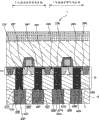
将参考图1的示意性截面图描述根据本发明第一实施例的半导体器件的构造的第一示例。A first example of the configuration of the semiconductor device according to the first embodiment of the present invention will be described with reference to the schematic cross-sectional view of FIG. 1 .
如图1所示,基板10具有形成在第一绝缘膜11上的半导体区域12。第一绝缘膜11由例如硅氮化物(SiN)膜、硅氧化物(SiO2)膜、硅碳氧化物(SiOC)膜、硅碳氧氮化物(SiOCN)膜或者它们的组合膜形成。备选地,第一绝缘膜11由诸如有机绝缘膜或类似物的绝缘膜形成,该绝缘膜由用于典型的半导体器件的层间绝缘层的材料制成。半导体区域12由例如硅层形成。As shown in FIG. 1 , a
半导体区域12具有元件隔离区域13,用于使P沟道晶体管形成区域和N沟道晶体管形成区域彼此分离。The
P沟道晶体管1P形成在PMOS晶体管形成区域的半导体区域12中,N沟道晶体管1N形成在NMOS晶体管形成区域的半导体区域12中。The P-
下文中,将描述细节。Hereinafter, details will be described.
栅极电极22P隔着栅极绝缘膜21P形成在半导体区域12的P沟道晶体管形成区域上。The
栅极绝缘膜21P由例如铪氧化物(HfO2)、硅氧氮化铪(HfSiON)、锆氧化物(ZrO2)、硅氧氮化锆(ZrSiON)或者类似物的所谓的高介电常数(高k)膜形成。备选地,栅极绝缘膜21P由热氧氮化物膜和高介电常数膜的组合膜形成。The
栅极电极22P由例如多晶硅制成。备选地,栅极电极22P由钛氮化物(TiN)、钽碳化物(TaC)、钨(W)或者类似物制成。
侧壁部23P和24P形成在栅极电极22P的侧壁处。侧壁部23P和24P由例如硅氧化物(SiO2)、硅氮化物(SiN)、硅氧氮化物(SiON)或者类似物制成。备选地,侧壁部23P和24P由这些材料的组合膜形成。
扩散层25P和26P形成在栅极电极22P两侧的半导体区域12中。扩散层25P和26P为p型且形成源极区域和漏极区域。扩散层25P和26P之间的半导体区域12形成沟道区域。Diffusion layers 25P and 26P are formed in
低阻抗部27P和28P形成在扩散层25P和26P的前表面处,从而具有低于扩散层25P和26P的阻抗(电阻)。低阻抗部27P和28P由例如硅化物层形成。硅化物层由例如钴(Co)、镍(Ni)、铂(Pt)、钽(Ta)、钛(Ti)或类似物的金属硅化物制成。
当栅极电极22P由多晶硅制成时,低阻抗部29P形成在栅极电极22P的上部处。低阻抗部29P由与以上所描述相同的硅化物层形成。When the
这样,P沟道晶体管1P形成在半导体区域12中。In this way, a P-
栅极电极22N隔着栅极绝缘膜21N形成在半导体区域12的N沟道晶体管形成区域上。The
栅极绝缘膜21N由例如铪氧化物(HfO2)、硅氧氮化铪(HfSiON)、锆氧化物(ZrO2)、硅氧氮化锆(ZrSiON)或者类似物的所谓的高介电常数(高k)膜形成。备选地,栅极绝缘膜21N由热氧氮化物膜和高介电常数膜的组合膜形成。The
栅极电极22N由例如多晶硅制成。备选地,栅极电极22N由钛氮化物(TiN)、钽碳化物(TaC)、钨(W)或者类似物制成。The
侧壁部23N和24N形成在栅极电极22N的侧壁处。侧壁部23N和24N由例如硅氧化物(SiO2)、硅氮化物、硅氧氮化物或者类似物制成。备选地,侧壁部23N和24N由这些材料的组合膜形成。
扩散层25N和26N形成在栅极电极22N两侧的半导体区域12中。扩散层25N和26N为N型且形成源极区域和漏极区域。扩散层25N和26N之间的半导体区域12形成沟道区域。Diffusion layers 25N and 26N are formed in the
低阻抗部27N和28N形成在扩散层25N和26N的前表面处,从而具有低于扩散层25N和26N的阻抗(电阻)。低阻抗部27N和28N由例如硅化物层形成。硅化物层由例如钴(Co)、镍(Ni)、铂(Pt)、钽(Ta)、钛(Ti)或类似物的金属硅化物制成。Low-
当栅极电极22N由多晶硅制成时,低阻抗部29N形成在栅极电极22N的上部处。低阻抗部29N由与如上所述相同的硅化物层形成。When the
这样,N沟道晶体管1N形成在半导体区域12中。In this way, an N-
如上所述,半导体器件1具有P沟道晶体管1P和N沟道晶体管1N。As described above, the
其中形成有P沟道晶体管1P和N沟道晶体管1N的基板10具有作为绝缘层的第一绝缘膜11以及形成在第一绝缘膜11的顶表面处的半导体区域12。因此,半导体区域12实质上相当于SOI基板的SOI层。为此,形成在半导体区域12中的P沟道晶体管1P和N沟道晶体管1N可以是完全耗尽型晶体管。The
半导体器件1可以具有上述晶体管之一。The
层间绝缘层41形成在半导体区域12上,以覆盖半导体器件1。层间绝缘层41由例如硅氮化物(SiN)膜、硅氧化物(SiO2)膜、硅碳氧化物(SiOC)膜、硅碳氧氮化物(SiOCN)膜或者它们的组合膜形成。备选地,层间绝缘层41由诸如有机绝缘膜或类似物的绝缘膜形成,该绝缘膜由用于典型的半导体器件的层间绝缘层的材料制成。层间绝缘层41的表面被平坦化。An interlayer insulating
支撑基板51形成在层间绝缘层41上。支撑基板51的示例包括硅基板、玻璃基板、塑料基板以及类似物。The
接触孔61P和62P形成在第一绝缘膜11中,以分别与扩散层25P和26P相通。接触孔61P和62P分别穿过扩散层25P和26P且到达低阻抗部27P和28P的后表面。后接触电极63P和64P分别形成在接触孔61P和62P中且连接到低阻抗部27P和28P的后表面。后接触电极63P和64P分别通过用金属材料(例如,钛(Ti)、钛氮化物(TiN)、钽(Ta)、钽氮化物(TaN)、钨(W)、铜(Cu)或者类似物)填充接触孔61P和62P而形成。Contact holes 61P and 62P are formed in the first insulating
类似地,接触孔61N和62N形成在第一绝缘膜11中,以分别与扩散层25N和26N相通。接触孔61N和62N分别穿过扩散层25N和26N且到达低阻抗部27N和28N的后表面。后接触电极63N和64N分别形成在接触孔61N和62N中且连接到低阻抗部27N和28N的后表面。后接触电极63N和64N分别通过用金属材料(例如,钛(Ti)、钛氮化物(TiN)、钽(Ta)、钽氮化物(TaN)、钨(W)、铜(Cu)或者类似物)填充接触孔61N和62N而形成。Similarly,
第二绝缘膜14形成在第一绝缘膜11处。第二绝缘膜14由例如硅氮化物(SiN)膜、硅氧化物(SiO2)膜、硅碳氧化物(SiOC)膜、硅碳氧氮化物(SiOCN)膜或者它们的组合膜形成。备选地,第二绝缘膜14由诸如有机绝缘膜或类似物的绝缘膜形成,该绝缘膜由用于典型的半导体器件的层间绝缘层的材料制成。The second insulating
互连槽65P和66P形成在第二绝缘膜14中,以分别与后接触电极63P和64P相通。互连槽65P和66P分别到达后接触电极63P和64P。互连67P和68P分别形成在互连槽65P和66P中且连接到后接触电极63P和64P。互连67P和68P分别通过用金属材料(例如,钛(Ti)、钛氮化物(TiN)、钽(Ta)、钽氮化物(TaN)、钌(Ru)、铜(Cu)或者类似物,或者它们的组合膜)填充互连槽65P和66P而形成。
类似地,互连槽65N和66N形成在第二绝缘膜14中,以分别与后接触电极63N和64N相通。互连槽65N和66N分别到达后接触电极63N和64N。互连67N和68N分别形成在互连槽65N和66N中且连接到后接触电极63N和64N。互连67N和68N分别通过用金属材料(例如,钛(Ti)、钛氮化物(TiN)、钽(Ta)、钽氮化物(TaN)、钌(Ru)、铜(Cu)或者类似物,或者它们的组合膜)填充互连槽65N和66N而形成。Similarly,
尽管未示出,但可以形成第N互连以及连接第N层叠互连与第(N-1)互连的第(N-1)后接触电极(这里,N≥2)。也就是,互连可以以多层互连的形式形成。Although not shown, an Nth interconnection and a (N−1)th rear contact electrode (here, N≧2) connecting the Nth stacked interconnection and the (N−1)th interconnection may be formed. That is, interconnections may be formed in the form of multilayer interconnections.
在半导体器件1中,后接触电极63P、64P、63N和64N分别穿过扩散层25P、26P、25N和26N并直接连接到低阻抗部27P、28P、27N和28N。因此,例如,后接触电极63P与扩散层25P之间的接触阻抗值减小。类似地,后接触电极64P、63N和64N与扩散层26P、25N和26N之间的接触阻抗值减小。也就是,后接触电极63P、64P、63N和64N与扩散层25P、26P、25N和26N之间的接触阻抗值等于前接触电极(未示出)与扩散层25P、26P、25N和26N之间的接触阻抗值,该前接触电极从前表面连接到形成在扩散层25P、26P、25N和26N前表面处的低阻抗部27P、28P、27N和28N。In
因此,将不形成在相关技术中形成在栅极电极22P和22N上的接触电极,从而栅极电极22P和22N与后接触电极63P、64P、63N和64N之间的寄生电容减小。Therefore, the contact electrodes formed on the
即使栅极电极22P和22N与接触电极之间的距离在平面布局方面随着元件的微型化而减小时,栅极电极22P和22N也能够与后接触电极63P、64P、63N和64N可靠地绝缘。Even when the distance between the
接触电极的微型化通过后接触电极63P、64P、63N和64N的小的深宽比而促进。Miniaturization of the contact electrodes is facilitated by the small aspect ratio of the
即使当所谓的应力衬垫膜(stress liner film)(未示出)设置在晶体管上以改善迁移率时,该应力衬垫膜也不被接触电极分开,因此应力衬垫膜的应力效应的损失是小的。应力衬垫膜(CSIL:沟道应力诱生衬垫)典型地由具有拉应力或压应力的硅氮化物膜形成。Even when a so-called stress liner film (not shown) is provided on the transistor to improve mobility, the stress liner film is not separated by the contact electrodes, so the loss of the stress effect of the stress liner film is small. A stress liner film (CSIL: Channel Stress Inducing Liner) is typically formed of a silicon nitride film having tensile stress or compressive stress.
[半导体器件构造的第二示例][Second Example of Semiconductor Device Configuration]
接下来,将参考图2的示意性截面图描述根据本发明第一实施例的半导体器件的构造的第二示例。图2中示出的半导体器件(晶体管)可以是以上所描述的P沟道晶体管1P或N沟道晶体管1N。也就是,提供连接到栅极电极和扩散层的共享接触电极。Next, a second example of the configuration of the semiconductor device according to the first embodiment of the present invention will be described with reference to the schematic cross-sectional view of FIG. 2 . The semiconductor device (transistor) shown in FIG. 2 may be the P-
如图2所示,基板10具有形成在第一绝缘膜11上的半导体区域12。第一绝缘膜11由例如硅氮化物(SiN)膜、硅氧化物(SiO2)膜、硅碳氧化物(SiOC)膜、硅碳氧氮化物(SiOCN)膜或者它们的组合膜形成。备选地,第一绝缘膜11由诸如有机绝缘膜或类似物的绝缘膜形成,该绝缘膜由用于典型的半导体器件的层间绝缘层的材料制成。半导体区域12由例如硅层形成。As shown in FIG. 2 , the
半导体区域12具有元件隔离区域13,用于分离晶体管形成区域。The
第一晶体管101(例如,P沟道晶体管或N沟道晶体管)形成在晶体管形成区域的半导体区域12中。A first transistor 101 (for example, a P-channel transistor or an N-channel transistor) is formed in the
下文中,将描述细节。Hereinafter, details will be described.
栅极电极22隔着栅极绝缘膜21形成在半导体区域12的晶体管形成区域上。The
栅极绝缘膜21由例如铪氧化物(HfO2)、硅氧氮化铪(HfSiON)、锆氧化物(ZrO2)、硅氧氮化锆(ZrSiON)或者类似物的所谓的高介电常数(高k)膜形成。备选地,栅极绝缘膜21由热氧氮化物膜和高介电常数膜的组合膜形成。The
栅极电极22由例如多晶硅制成。
侧壁部23和24形成在栅极电极22的侧壁处。侧壁部23和24由例如硅氧化物(SiO2)、硅氮化物(SiN)、硅氧氮化物(SiON)或者类似物制成。备选地,侧壁部23和24由这些材料的组合膜形成。
扩散层25和26形成在栅极电极22两侧的半导体区域12中。扩散层25和26在P沟道晶体管的情况下为P型或者在N沟道晶体管的情况下为N型,且形成源极区域和漏极区域。扩散层25和26之间的半导体区域12形成沟道区域。Diffusion layers 25 and 26 are formed in the
低阻抗部27和28分别形成在扩散层25和26的前表面处,以具有低于扩散层25和26的阻抗(电阻)。低阻抗部27和28由例如硅化物层形成。硅化物层由例如钴(Co)、镍(Ni)、铂(t)、钽(Ta)、钛(Ti)或类似物的金属硅化物制成。Low-
低阻抗部29形成在栅极电极22的上部处。低阻抗部29由与以上所描述相同的硅化物层形成。
这样,第一晶体管101形成在半导体区域12中。In this way, the
不同于第一晶体管101的第二晶体管102的栅极电极122形成为在元件隔离区域13上延伸。栅极电极122由多晶硅制成,且低阻抗部129形成在栅极电极122上。低阻抗部129由与以上所描述相同的硅化物层形成。The
层间绝缘层41形成在半导体区域12上,以覆盖半导体器件2(第一晶体管101和第二晶体管102)。层间绝缘层41由例如硅氮化物(SiN)膜、硅氧化物(SiO2)膜、硅碳氧化物(SiOC)膜、硅碳氧氮化物(SiOCN)膜或者它们的组合膜形成。备选地,层间绝缘层41由诸如有机绝缘膜或类似物的绝缘膜形成,该绝缘膜由用于典型的半导体器件的层间绝缘层的材料制成。层间绝缘层41的表面被平坦化。An interlayer insulating
支撑基板51形成在层间绝缘层41上。支撑基板51的示例包括硅基板、玻璃基板、塑料基板以及类似物。The
接触孔61和62形成在第一绝缘膜11中,以分别与扩散层25和26相通。接触孔61和62分别穿过扩散层25和26且到达低阻抗部27和28的后表面。其中,接触孔62还到达栅极电极122的低阻抗部129的后表面。后接触电极63和64分别形成在接触孔61和62中且连接到低阻抗部27和28的后表面。其中,后接触电极64连接到栅极电极122的低阻抗部129和扩散层26的低阻抗部28。后接触电极63和64分别通过用金属材料(例如,钛(Ti)、钛氮化物(TiN)、钽(Ta)、钽氮化物(TaN)、钨(W)、铜(Cu)或者类似物)填充接触孔61和62而形成。Contact holes 61 and 62 are formed in the first insulating
第二绝缘膜14形成在第一绝缘膜11处。第二绝缘膜14由例如硅氮化物(SiN)膜、硅氧化物(SiO2)膜、硅碳氧化物(SiOC)膜、硅碳氧氮化物(SiOCN)膜或者它们的组合膜形成。备选地,第二绝缘膜14由诸如有机绝缘膜或类似物的绝缘膜形成,该绝缘膜由用于典型的半导体器件的层间绝缘层的材料制成。The second insulating
互连槽65和66形成在第二绝缘膜14中,以分别与后接触电极63和64相通。互连槽65和66分别到达后接触电极63和64。互连67和68分别形成在互连槽65和66中且连接到后接触电极63和64。互连67和68分别通过用金属材料(例如,钛(Ti)、钛氮化物(TiN)、钽(Ta)、钽氮化物(TaN)、钌(Ru)、铜(Cu)或者类似物,或者它们的组合膜)填充互连槽65和66而形成。
尽管未示出,但可以形成第N互连以及连接第N层叠互连与第(N-1)互连的第(N-1)后接触电极(这里,N≥2)。也就是,互连可以以多层互连的形式形成。Although not shown, an Nth interconnection and a (N−1)th rear contact electrode (here, N≧2) connecting the Nth stacked interconnection and the (N−1)th interconnection may be formed. That is, interconnections may be formed in the form of multilayer interconnections.
半导体器件2应用于所谓的共享接触电极结构。因此,即使在共享接触电极结构中,也获得与半导体器件1相同的优点。与半导体器件1类似,半导体器件2可以具有完全耗尽型晶体管。The semiconductor device 2 is applied to a so-called shared contact electrode structure. Therefore, even in the shared contact electrode structure, the same advantages as those of the
也就是,与半导体器件1类似,在半导体器件2中,后接触电极63和64分别穿过扩散层25和26直接连接到低阻抗部27和28。因此,例如,后接触电极63与扩散层25之间的接触阻抗值减小。类似地,后接触电极64与扩散层26之间的接触阻抗值减小。也就是,后接触电极63和64与扩散层25和26之间的接触阻抗值等于前接触电极(未示出)与扩散层25和26之间的接触阻抗值,该前接触电极从前表面连接到形成在扩散层25和26前表面处的低阻抗部27和28。That is, similarly to
因此,将不形成在相关技术中形成在栅极电极22上的接触电极,从而栅极电极22与后接触电极63和64之间的寄生电容减小。Therefore, the contact electrode formed on the
即使栅极电极22与接触电极之间的距离在平面布局方面随着元件的微型化而减小时,栅极电极22也能够与后接触电极63和64可靠地绝缘。Even when the distance between the
接触电极的微型化通过后接触电极63和64的小的深宽比而促进。The miniaturization of the contact electrodes is facilitated by the small aspect ratio of the
即使当所谓的应力衬垫膜(stress liner film)(未示出)设置在晶体管上以改善迁移率时,该应力衬垫膜也不被接触电极分开,因此应力衬垫膜的应力效应的损失是小的。应力衬垫膜(CSIL:沟道应力诱生衬垫)典型地由具有拉应力或压应力的硅氮化物膜形成。Even when a so-called stress liner film (not shown) is provided on the transistor to improve mobility, the stress liner film is not separated by the contact electrodes, so the loss of the stress effect of the stress liner film is small. A stress liner film (CSIL: Channel Stress Inducing Liner) is typically formed of a silicon nitride film having tensile stress or compressive stress.
[半导体器件构造的第三示例][Third Example of Semiconductor Device Configuration]
接下来,将参考图3的示意性截面图描述根据本发明第一实施例的半导体器件的构造的第三示例。Next, a third example of the configuration of the semiconductor device according to the first embodiment of the present invention will be described with reference to the schematic cross-sectional view of FIG. 3 .
如图3所示,半导体器件3具有形成在半导体区域12中的P沟道晶体管3P和N沟道晶体管3N。半导体器件3与上述半导体器件1的不同之处在于:代替形成在栅极电极22P的侧壁处的侧壁部23P和24P(见图1)而设置空间91P和92P。此外,代替形成在栅极电极22N的侧壁处的侧壁部23N和24N(见图1)而设置空间91N和92N。As shown in FIG. 3 , the
第一层间绝缘层42隔着空间91P和92P形成于栅极电极22P的侧方。第一层间绝缘层42隔着空间91N和92N形成于栅极电极22N的侧方。The first
第二层间绝缘层43形成在第一层间绝缘层42上,使得其不填充空间91P和92P及空间91N和92N。因此,第一层间绝缘层42和第二层间绝缘层43形成层间绝缘层41。The second insulating
其他部件与参考图1所描述的相同。Other components are the same as described with reference to FIG. 1 .
在半导体器件3中,空间91P和92P可以在栅极电极22P的侧方形成,空间91N和92N可以在栅极电极22N的侧方形成,因此寄生电容可以被进一步减小。此外,获得与半导体器件1相同的优点。与半导体器件1类似,半导体器件3可以具有完全耗尽型晶体管。In the
[半导体器件构造的第四示例][Fourth Example of Semiconductor Device Configuration]
接下来,将参考图1的示意性截面图描述根据本发明第一实施例的半导体器件的构造的第四示例。Next, a fourth example of the configuration of the semiconductor device according to the first embodiment of the present invention will be described with reference to the schematic cross-sectional view of FIG. 1 .
如图1所示,半导体器件的构造的第四示例被构造为使得侧壁部23P和24P及侧壁部23N和24N由例如介电常数低于硅氧化物的低介电常数膜形成。低介电常数膜的示例包括有机绝缘膜。As shown in FIG. 1 , a fourth example of the configuration of a semiconductor device is configured such that
这样,侧壁部23P和24P及侧壁部23N和24N由低介电常数膜形成,因此,寄生电容可以被进一步减小。In this way, the
[半导体器件构造的第五示例][Fifth Example of Semiconductor Device Configuration]
接下来,将参考图4的示意性截面图描述根据本发明第一实施例的半导体器件的构造的第五示例。Next, a fifth example of the configuration of the semiconductor device according to the first embodiment of the present invention will be described with reference to the schematic cross-sectional view of FIG. 4 .
如图4所示,基板10具有形成在第一绝缘膜11上的半导体区域12。第一绝缘膜11由例如硅氮化物(SiN)膜、硅氧化物(SiO2)膜、硅碳氧化物(SiOC)膜、硅碳氧氮化物(SiOCN)膜或者它们的组合膜形成。备选地,第一绝缘膜11由诸如有机绝缘膜或类似物的绝缘膜形成,该绝缘膜由用于典型的半导体器件的层间绝缘层的材料制成。半导体区域12由例如硅层形成。As shown in FIG. 4 , the
半导体区域12具有元件隔离区域13,用于使P沟道晶体管形成区域和N沟道晶体管形成区域彼此分离。The
P沟道晶体管5P形成在PMOS晶体管形成区域的半导体区域12中,N沟道晶体管5N形成在NMOS晶体管形成区域的半导体区域12中。The P-
下文中,将描述细节。Hereinafter, details will be described.
栅极电极22P隔着栅极绝缘膜21P形成在半导体区域12的P沟道晶体管形成区域上。The
栅极绝缘膜21P由例如铪氧化物(HfO2)、硅氧氮化铪(HfSiON)、锆氧化物(ZrO2)、硅氧氮化锆(ZrSiON)或者类似物的所谓的高介电常数(高k)膜形成。备选地,栅极绝缘膜21P由热氧氮化物膜和高介电常数膜的组合膜形成。The
栅极电极22P由例如多晶硅制成。备选地,栅极电极22P由钛氮化物(TiN)、钽碳化物(TaC)、钨(W)或者类似物制成。
侧壁部23P和24P形成在栅极电极22P的侧壁处。侧壁部23P和24P由例如硅氧化物(SiO2)、硅氮化物(SiN)、硅氧氮化物(SiON)或者类似物制成。备选地,侧壁部23P和24P由这些材料的组合膜形成。
扩散层25P和26P形成在栅极电极22P两侧的半导体区域12中。扩散层25P和26P为p型且形成源极区域和漏极区域。扩散层25P和26P之间的半导体区域12形成沟道区域。Diffusion layers 25P and 26P are formed in
这样,P沟道晶体管5P形成在半导体区域12中。In this way, P-
栅极电极22N隔着栅极绝缘膜21N形成在半导体区域12的N沟道晶体管形成区域上。The
栅极绝缘膜21N由例如铪氧化物(HfO2)、硅氧氮化铪(HfSiON)、锆氧化物(ZrO2)、硅氧氮化锆(ZrSiON)或者类似物的所谓的高介电常数(高k)膜形成。备选地,栅极绝缘膜21N由热氧氮化物膜和高介电常数膜的组合膜形成。The
栅极电极22N由例如多晶硅制成。备选地,栅极电极22N由钛氮化物(TiN)、钽碳化物(TaC)、钨(W)或者类似物制成。The
侧壁部23N和24N形成在栅极电极22N的侧壁处。侧壁部23N和24N由例如硅氧化物(SiO2)、硅氮化物、硅氧氮化物或者类似物制成。备选地,侧壁部23N和24N由这些材料的组合膜形成。
扩散层25N和26N形成在栅极电极22N两侧的半导体区域12中。扩散层25N和26N为N型且形成源极区域和漏极区域。扩散层25N和26N之间的半导体区域12形成沟道区域。Diffusion layers 25N and 26N are formed in the
这样,N沟道晶体管5N形成在半导体区域12中。In this way, the N-
如上所述,半导体器件5具有P沟道晶体管5P和N沟道晶体管5N。与半导体器件1类似,半导体器件5可以具有完全耗尽型晶体管。半导体器件5可以具有上述晶体管之一。As described above, the
层间绝缘层41形成在半导体区域12上,以覆盖半导体器件5。层间绝缘层41由例如硅氮化物(SiN)膜、硅氧化物(SiO2)膜、硅碳氧化物(SiOC)膜、硅碳氧氮化物(SiOCN)膜或者它们的组合膜形成。备选地,层间绝缘层41由诸如有机绝缘膜或类似物的绝缘膜形成,该绝缘膜由用于典型的半导体器件的层间绝缘层的材料制成。层间绝缘层41的表面被平坦化。An interlayer insulating
电极(接触电极)44P和45P形成在层间绝缘层41中,以分别连接到扩散层25P和26P的前表面。电极44P和45P成为低阻抗部件。此外,电极(接触电极)44N和45N形成为分别连接到扩散层25N和26N。电极44N和45N成为低阻抗部件。Electrodes (contact electrodes) 44P and 45P are formed in the
互连46P和47P形成为分别连接到电极44P和45P。互连46N和47N形成为分别连接到电极44N和45N。
支撑基板51形成在层间绝缘层41上。支撑基板51的示例包括硅基板、玻璃基板、塑料基板以及类似物。The
接触孔61P和62P形成在第一绝缘膜11中,以分别与扩散层25P和26P相通。接触孔61P和62P分别穿过扩散层25P和26P且到达电极44P和45P的后表面。后接触电极63P和64P分别形成在接触孔61P和62P中且连接到电极44P和45P的后表面。后接触电极63P和64P分别通过用金属材料,(例如,钛(Ti)、钛氮化物(TiN)、钽(Ta)、钽氮化物(TaN)、钨(W)、铜(Cu)或者类似物)填充接触孔61P和62P而形成。Contact holes 61P and 62P are formed in the first insulating
类似地,接触孔61N和62N形成在第一绝缘膜11中,以分别与扩散层25N和26N相通。接触孔61N和62N分别穿过扩散层25N和26N且到达电极44N和45N的后表面。后接触电极63N和64N分别形成在接触孔61N和62N中且连接到电极44N和45N的后表面。后接触电极63N和64N分别通过用金属材料(例如,钛(Ti)、钛氮化物(TiN)、钽(Ta)、钽氮化物(TaN)、钨(W)、铜(Cu)或者类似物)填充接触孔61N和62N而形成。Similarly,
第二绝缘膜14形成在第一绝缘膜11处。第二绝缘膜14由例如硅氮化物(SiN)膜、硅氧化物(SiO2)膜、硅碳氧化物(SiOC)膜、硅碳氧氮化物(SiOCN)膜或者它们的组合膜形成。备选地,第二绝缘膜14由诸如有机绝缘膜或类似物的绝缘膜形成,该绝缘膜由用于典型的半导体器件的层间绝缘层的材料制成。The second insulating
互连槽65P和66P形成在第二绝缘膜14中,以分别与后接触电极63P和64P相通。互连槽65P和66P分别到达后接触电极63P和64P。互连67P和68P分别形成在互连槽65P和66P中且连接到后接触电极63P和64P。互连67P和68P分别通过用金属材料(例如,钛(Ti)、钛氮化物(TiN)、钽(Ta)、钽氮化物(TaN)、钌(Ru)、铜(Cu)或者类似物,或者它们的组合膜)填充互连槽65P和66P而形成。
类似地,互连槽65N和66N形成在第二绝缘膜14中,以分别与后接触电极63N和64N相通。互连槽65N和66N分别到达后接触电极63N和64N。互连67N和68N分别形成在互连槽65N和66N中且连接到后接触电极63N和64N。互连67N和68N分别通过用金属材料(例如,钛(Ti)、钛氮化物(TiN)、钽(Ta)、钽氮化物(TaN)、钌(Ru)、铜(Cu)或者类似物,或者它们的组合膜)填充互连槽65N和66N而形成。Similarly,
尽管未示出,但可以形成第N互连以及连接第N层叠互连与第(N-1)互连的第(N-1)后接触电极(这里,N≥2)。也就是,互连可以以多层互连的形式形成。Although not shown, an Nth interconnection and a (N−1)th rear contact electrode (here, N≧2) connecting the Nth stacked interconnection and the (N−1)th interconnection may be formed. That is, interconnections may be formed in the form of multilayer interconnections.
在半导体器件5中,后接触电极63P、64P、63N和64N分别穿过扩散层25P、26P、25N和26N直接连接到电极44P、45P、44N和45N。因此,例如,后接触电极63P与扩散层25P之间的接触阻抗值减小。类似地,后接触电极64P、63N和64N与扩散层26P、25N和26N之间的接触阻抗值减小。也就是,后接触电极63P、64P、63N和64N与扩散层25P、26P、25N和26N之间的接触阻抗值等于前接触电极(未示出)与扩散层25P、26P、25N和26N之间的接触阻抗值,该前接触电极从前表面连接到形成在扩散层25P、26P、25N和26N前表面处的电极44P、45P、44N和45N。In
因此,将不形成在相关技术中形成在栅极电极22P和22N上的接触电极,从而栅极电极22P和22N与后接触电极63P、64P、63N和64N之间的寄生电容减小。Therefore, the contact electrodes formed on the
即使栅极电极22P和22N与接触电极之间的距离在平面布局方面随着元件的微型化而减小时,栅极电极22P和22N也能够与后接触电极63P、64P、63N和64N可靠地绝缘。Even when the distance between the
接触电极的微型化通过后接触电极63P、64P、63N和64N的小的深宽比而促进。Miniaturization of the contact electrodes is facilitated by the small aspect ratio of the
即使当所谓的应力衬垫膜(未示出)设置在晶体管上以改善迁移率时,该应力衬垫膜也不被接触电极分开,因此应力衬垫膜的应力效应的损失是小的。应力衬垫膜(CSIL:沟道应力诱生衬垫)典型地由具有拉应力或压应力的硅氮化物膜形成。Even when a so-called stress liner film (not shown) is provided on the transistor to improve mobility, the stress liner film is not separated by the contact electrodes, so the loss of the stress effect of the stress liner film is small. A stress liner film (CSIL: Channel Stress Inducing Liner) is typically formed of a silicon nitride film having tensile stress or compressive stress.
<2.第二实施例><2. Second Embodiment>
[半导体器件构造的第六示例][Sixth Example of Semiconductor Device Configuration]
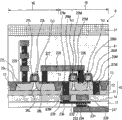
将参考图5的示意性截面图描述根据本发明第二实施例的半导体器件的构造的第六示例。图5示出了其中用作存储元件的电容器形成在基板10的后表面上的示例。A sixth example of the configuration of the semiconductor device according to the second embodiment of the present invention will be described with reference to the schematic cross-sectional view of FIG. 5 . FIG. 5 shows an example in which capacitors serving as storage elements are formed on the rear surface of the
如图5所示,基板10具有形成在第一绝缘膜11上的半导体区域12。第一绝缘膜11由例如硅氮化物(SiN)膜、硅氧化物(SiO2)膜、硅碳氧化物(SiOC)膜、硅碳氧氮化物(SiOCN)膜或者它们的组合膜形成。备选地,第一绝缘膜11由诸如有机绝缘膜或类似物的绝缘膜形成,该绝缘膜由用于典型的半导体器件的层间绝缘层的材料制成。半导体区域12由例如硅层形成。As shown in FIG. 5 , a
半导体区域12具有元件隔离区域13,用于分离存储元件部15和逻辑元件部16。元件隔离区域13具有例如浅沟槽隔离(STI,Shallow TrenchIsolation)结构且通过利用硅氧化物填充形成在半导体区域12中的元件隔离槽而形成。The
第一场效应晶体管Tr1形成在存储元件部15的半导体区域12中,第二场效应晶体管Tr2形成在逻辑元件部16的半导体区域12中。The first field effect transistor Tr1 is formed in the
第一场效应晶体管Tr1具有隔着栅极绝缘膜21M形成在半导体区域12的前表面上的栅极电极22M。成为源极区域和漏极区域的扩散层25M和26M形成在栅极电极22M两侧的半导体区域12中。低阻抗部27M和28M分别形成在扩散层25M和26M的前表面处。在扩散层25M和26M之间的一部分半导体区域12成为第一场效应晶体管Tr1的沟道区域。The first field effect transistor Tr1 has a
栅极绝缘膜21M、栅极电极22M及低阻抗部27M和28M由与半导体器件1的栅极绝缘膜、栅极电极和低阻抗部相同的材料制成。The
第二场效应晶体管Tr2具有隔着栅极绝缘膜21L形成在半导体区域12的前表面上的栅极电极22L。成为源极区域和漏极区域的扩散层25L和26L形成在栅极电极22L两侧的半导体区域12中。在扩散层25L和26L之间的一部分半导体区域12成为第二场效应晶体管Tr2的沟道区域。The second field effect transistor Tr2 has a
栅极绝缘膜21L、栅极电极22L及低阻抗部27L和28L由与半导体器件1的栅极绝缘膜、栅极电极和低阻抗部相同的材料制成。The
层间绝缘层41形成在半导体区域12的前表面上,以覆盖第一场效应晶体管Tr1和第二场效应晶体管Tr2。层间绝缘层41形成为具有例如几百nm或更大的厚度,且层间绝缘层41的表面被平坦化。An interlayer insulating
支撑基板51形成在层间绝缘层41上。The
后接触电极64M形成在第一绝缘膜11中,以连接到扩散层26M。形成例如电容器211作为连接到后接触电极64M的存储元件。A
电容器211具有第一电极212和形成在第一电极212的前表面上的第二电极214,且第一电极212与第二电极214之间插设有电容器绝缘膜213。The capacitor 211 has a
扩散层26M和第一电极212通过后接触电极64M彼此电连接,后接触电极64M穿过第一绝缘膜11和扩散层26M并连接到低阻抗部28M的后表面。The
第二绝缘膜14形成在第一绝缘膜11上以覆盖电容器211。The second insulating
在半导体器件6中,当电容器211安装到逻辑器件上时,在相关技术中形成在前表面上的电容器211可以布置在后表面上。因此,可以应用微型化的规则,从而可以易于形成高容量的存储器。In the semiconductor device 6, when the capacitor 211 is mounted on the logic device, the capacitor 211 formed on the front surface in the related art may be arranged on the rear surface. Therefore, the rule of miniaturization can be applied, so that a high-capacity memory can be easily formed.
电容器211和用作存取晶体管的第一场效应晶体管Tr1可以在浅的后接触电极64M处彼此连接。因此,实现了接触阻抗的降低、MOSFET性能的改善以及接触电极良率的改善。The capacitor 211 and the first field effect transistor Tr1 serving as an access transistor may be connected to each other at the shallow
[半导体器件构造的第七示例][Seventh Example of Semiconductor Device Configuration]
接下来,将参考图6的示意性截面图描述根据本发明第二实施例的半导体器件的构造的第七示例。图6示出了其中用作存储元件的阻变存储元件形成在基板10的后表面上的示例。Next, a seventh example of the configuration of the semiconductor device according to the second embodiment of the present invention will be described with reference to the schematic cross-sectional view of FIG. 6 . FIG. 6 shows an example in which a resistive memory element serving as a memory element is formed on the rear surface of the
如图6所示,基板10具有形成在第一绝缘膜11上的半导体区域12。第一绝缘膜11由例如硅氮化物(SiN)膜、硅氧化物(SiO2)膜、硅碳氧化物(SiOC)膜、硅碳氧氮化物(SiOCN)膜或者它们的组合膜形成。备选地,第一绝缘膜11由诸如有机绝缘膜或类似物的绝缘膜形成,该绝缘膜由用于典型的半导体器件的层间绝缘层的材料制成。半导体区域12由例如硅层形成。As shown in FIG. 6 , a
半导体区域12具有元件隔离区域13,用于分离存储元件部15和逻辑元件部16。元件隔离区域13具有例如浅沟槽隔离(STI)结构且通过利用硅氧化物填充形成在半导体区域12中的元件隔离槽而形成。The
共享单个扩散层的第一场效应晶体管Tr1和第二场效应晶体管Tr2形成为在存储元件部15的半导体区域12中彼此相邻。第三场效应晶体管Tr3形成在逻辑元件部16的半导体区域12中。The first field effect transistor Tr1 and the second field effect transistor Tr2 sharing a single diffusion layer are formed adjacent to each other in the
第一场效应晶体管Tr1和第二场效应晶体管Tr2的每个具有隔着栅极绝缘膜21M形成在半导体区域12的前表面上的栅极电极22M。成为源极区域和漏极区域的扩散层25M和26M形成在栅极电极22M两侧的半导体区域12中。扩散层26M被共享。低阻抗部27M和28M分别形成在扩散层25M和26M的前表面处。在一侧(图中的左侧)的扩散层25M和26M之间的半导体区域12成为第一场效应晶体管Tr1的沟道区域。在另一侧(图中的右侧)的扩散层25M和26M之间的半导体区域12成为第二场效应晶体管Tr2的沟道区域。Each of the first field effect transistor Tr1 and the second field effect transistor Tr2 has a
栅极绝缘膜21M、栅极电极22M及低阻抗部27M和28M由与半导体器件1的栅极绝缘膜、栅极电极和低阻抗部相同的材料制成。The
第三场效应晶体管Tr3具有隔着栅极绝缘膜21L形成在半导体区域12的前表面上的栅极电极22L。成为源极区域和漏极区域的扩散层25L和26L形成在栅极电极22L两侧的半导体区域12中。低阻抗部27L和28L分别形成在扩散层25L和26L的前表面处。在扩散层25L和26L之间的一部分半导体区域12成为第三场效应晶体管Tr3的沟道区域。The third field effect transistor Tr3 has a
栅极绝缘膜21L、栅极电极22L及低阻抗部27L和28L由与半导体器件1的栅极绝缘膜、栅极电极和低阻抗部相同的材料制成。The
层间绝缘层41形成在半导体区域12的前表面上,以覆盖第一场效应晶体管Tr1、第二场效应晶体管Tr2和第三场效应晶体管Tr3等。层间绝缘层41形成为具有例如几百nm或更大的厚度,且层间绝缘层41的表面被平坦化。An interlayer insulating
支撑基板51形成在层间绝缘层41上。The
后接触电极63M形成在第一绝缘膜11中,以连接到扩散层25M。阻变存储元件221形成为连接到后接触电极63M。A
阻变存储元件221通过层叠第一电极222、存储层223、离子源层224和第二电极225而形成。The
第一电极222和第二电极225由例如铂(Pt)、钨(W)、钨氮化物(WN)、铜(Cu)或者类似物制成。The
存储层(阻变膜)223由金属氧化物制成。金属氧化物的示例包括钽氧化物、铌氧化物、铝氧化物、镍氧化物、钴氧化物、钛氧化物、铪氧化物、锆氧化物、镓氧化物或者类似物,或者它们的混合。存储层223优选是薄的,且形成为具有等于或小于2nm(优选等于或小于1nm,更优选等于或小于0.5nm)的厚度。The storage layer (resistive switch film) 223 is made of metal oxide. Examples of metal oxides include tantalum oxides, niobium oxides, aluminum oxides, nickel oxides, cobalt oxides, titanium oxides, hafnium oxides, zirconium oxides, gallium oxides, or the like, or mixtures thereof. The
离子源层224包含例如铜(Cu)、银(Ag)和锌(Zn)的至少之一以及诸如碲(Te)、硒(Se)和硫(S)的硫族化物元素的至少之一。例如,CuTe、GeSbTe、CuGeTe、AgGeTe、AgTe、ZnTe、ZnGeTe、CuS、CuGeS、CuSe、CuGeSe及类似物可以为示例。离子源层224可以包含硼(B)、稀土元素或者硅(Si)。The
因此,离子源层224包含Cu、Ag和Zn的至少之一。也就是,离子源层224是用于向存储层223提供Cu、Ag和Zn的至少之一的离子的层,或者是用于接收提供给存储层223的离子的层。Therefore, the
扩散层25M和第一电极222通过后接触电极63M彼此电连接,后接触电极63M穿过第一绝缘膜11和扩散层25M并连接到低阻抗部27M的后表面。The
在图中,第二电极225用作互连。为此,第二绝缘膜14形成为埋入第一电极222、存储层223和离子源层224,而第二电极225连接到离子源层224且布置在第二绝缘膜14上。In the figure, the
接触电极226连接到第一场效应晶体管Tr1的扩散层26M,接触电极227连接到第三场效应晶体管Tr3的扩散层26L。接触电极226和接触电极227通过互连228彼此连接。从而,第一场效应晶体管Tr1的扩散层26M电连接到第三场效应晶体管Tr3的扩散层26L。通过在多层(图中为三层)中层叠接触电极和互连而形成的多层互连部229连接到第三场效应晶体管Tr3的扩散层25L。The
在半导体器件7中,当阻变存储元件221安装在逻辑器件上时,在相关技术中形成在最上面的互连上的阻变存储元件221可以布置在后表面上。因此,可以应用微型化规则,从而可以易于形成高容量的存储器。In the
阻变存储元件221和用作存取晶体管的第一场效应晶体管Tr1及第二场效应晶体管Tr2可以在浅的后接触电极63M处彼此连接。因此,实现了接触阻抗的降低、MOSFET性能的改善以及接触电极良率的改善。The
[半导体器件构造的第八示例][Eighth Example of Semiconductor Device Configuration]
接下来,将参考图7的示意性截面图描述根据本发明第二实施例的半导体器件的构造的第八示例。图7示出了其中用作存储元件的磁阻存储元件形成在基板10的后表面上的示例。Next, an eighth example of the configuration of the semiconductor device according to the second embodiment of the present invention will be described with reference to the schematic cross-sectional view of FIG. 7 . FIG. 7 shows an example in which a magnetoresistive memory element serving as a memory element is formed on the rear surface of the
如图7所示,基板10具有形成在第一绝缘膜11上的半导体区域12。第一绝缘膜11由例如硅氮化物(SiN)膜、硅氧化物(SiO2)膜、硅碳氧化物(SiOC)膜、硅碳氧氮化物(SiOCN)膜或者它们的组合膜形成。备选地,第一绝缘膜11由诸如有机绝缘膜或类似物的绝缘膜形成,该绝缘膜由用于典型的半导体器件的层间绝缘层的材料制成。半导体区域12由例如硅层形成。As shown in FIG. 7 , a
半导体区域12具有元件隔离区域13,用于分离存储元件部15和逻辑元件部16。元件隔离区域13具有例如浅沟槽隔离(STI)结构且通过利用硅氧化物填充形成在半导体区域12中的元件隔离槽而形成。The
共享单个扩散层的第一场效应晶体管Tr1和第二场效应晶体管Tr2在存储元件部15的半导体区域12中形成为彼此相邻。第三场效应晶体管Tr3形成在逻辑元件部16的半导体区域12中。The first field effect transistor Tr1 and the second field effect transistor Tr2 sharing a single diffusion layer are formed adjacent to each other in the
第一场效应晶体管Tr1和第二场效应晶体管Tr2的每个具有隔着栅极绝缘膜21M形成在半导体区域12的前表面上的栅极电极22M。成为源极区域和漏极区域的扩散层25M和26M形成在栅极电极22M两侧的半导体区域12中。扩散层26M被共享。低阻抗部27M和28M分别形成在扩散层25M和26M的前表面处。在一侧(图中的左侧)的扩散层25M和26M之间的半导体区域12成为第一场效应晶体管Tr1的沟道区域。在另一侧(图中的右侧)的扩散层25M和26M之间的半导体区域12成为第二场效应晶体管Tr2的沟道区域。Each of the first field effect transistor Tr1 and the second field effect transistor Tr2 has a
栅极绝缘膜21M、栅极电极22M及低阻抗部27M和28M由与半导体器件1的栅极绝缘膜、栅极电极和低阻抗部相同的材料制成。The
第三场效应晶体管Tr3具有隔着栅极绝缘膜21L形成在半导体区域12的前表面上的栅极电极22L。成为源极区域和漏极区域的扩散层25L和26L形成在栅极电极22L两侧的半导体区域12中。低阻抗部27L和28L分别形成在扩散层25L和26L的前表面处。在扩散层25L和26L之间的一部分半导体区域12成为第三场效应晶体管Tr3的沟道区域。The third field effect transistor Tr3 has a
栅极绝缘膜21L、栅极电极22L及低阻抗部27L和28L由与半导体器件1的栅极绝缘膜、栅极电极和低阻抗部相同的材料制成。The
层间绝缘层41形成在半导体区域12的前表面上,以覆盖第一场效应晶体管Tr1、第二场效应晶体管Tr2和第三场效应晶体管Tr3等。层间绝缘层41形成为具有例如几百nm或更大的厚度,且层间绝缘层41的表面被平坦化。An interlayer insulating
支撑基板51形成在层间绝缘层41上。The
后接触电极63M形成为穿过第一绝缘膜11和扩散层25M,且连接到低阻抗部27M的后表面。形成连接到后接触电极63M的互连235以及连接到互连235的接触电极236。The
写入线237形成在与互连235相同的层处。当电流在写入线237中流动时写入线237产生磁场且反转以下描述的MTJ膜233的自由层的磁化方向。写入线237由例如铜(Cu)、铝(Al)、钛(Ti)、钽(Ta)、钛氮化物(TiN)、钨(W)、钽氮化物(TaN)或者类似物制成。The
磁阻存储元件231隔着第二绝缘膜14形成在写入线237上。The
磁阻存储元件231通过层叠第一电极232、MTJ膜233和第二电极234而形成。第一电极232连接到接触电极236。The
第一电极232由例如钛氮化物(TiN)、钨(W)、铂(Pt)或者类似物制成。第二电极234由例如铂(Pt)制成。The
术语“MTJ”是磁隧道结的缩写,并表示磁隧道结。MTJ膜233形成为具有钉扎层(pinning layer)、隧道绝缘膜以及自由层的层叠结构。钉扎层由例如钴(Co)、钴铁硼(CoFeB)或者类似物制成。隧道绝缘膜由例如铝氧化物、镁氧化物或者类似物的氧化物膜形成。自由层由例如镍铁(NiFe)、钌(Ru)和镍铁(NiFe)的层叠膜、钴铁(CoFe)或者类似物形成。The term "MTJ" is an abbreviation for Magnetic Tunnel Junction, and means Magnetic Tunnel Junction. The
第三绝缘膜17形成为掩埋磁阻存储元件231。位线(或者电源线)238设置于第三绝缘膜17,以连接到磁阻存储元件231的第二电极234且沿与写入线237正交的方向延伸。The third
接触电极226连接到第一场效应晶体管Tr1的扩散层26M,接触电极227连接到第三场效应晶体管Tr3的扩散层26L。接触电极226和接触电极227通过互连228彼此连接。从而,第一场效应晶体管Tr1的扩散层26M电连接到第三场效应晶体管Tr3的扩散层26L。通过在多层(图中为三层)中层叠接触电极和互连而形成的多层互连部229连接到第三场效应晶体管Tr3的扩散层25L。The
在半导体器件8中,当磁阻存储元件231安装在逻辑器件上时,在相关技术中形成在最上面的互连上的阻变存储元件231可以布置在后表面上。因此,可以应用微型化规则,从而可以易于形成高容量的存储器。In the
磁阻存储元件231和用作存取晶体管的第一场效应晶体管Tr1可以在浅的后接触电极63M处彼此连接。因此,实现了接触阻抗的降低、MOSFET性能的改善以及接触电极良率的改善。The
[半导体器件构造的第九示例][Ninth Example of Semiconductor Device Configuration]
接下来,将参考图8的示意性截面图描述根据本发明第二实施例的半导体器件的构造的第九示例。图8示出了其中用作存储元件的阻变存储元件形成在基板10的后表面上的示例。Next, a ninth example of the configuration of the semiconductor device according to the second embodiment of the present invention will be described with reference to the schematic cross-sectional view of FIG. 8 . FIG. 8 shows an example in which a resistive memory element serving as a memory element is formed on the rear surface of the
如图8所示,基板10具有形成在第一绝缘膜11上的半导体区域12。第一绝缘膜11由例如硅氮化物(SiN)膜、硅氧化物(SiO2)膜、硅碳氧化物(SiOC)膜、硅碳氧氮化物(SiOCN)膜或者它们的组合膜形成。备选地,第一绝缘膜11由诸如有机绝缘膜或类似物的绝缘膜形成,该绝缘膜由用于典型的半导体器件的层间绝缘层的材料制成。半导体区域12由例如硅层形成。As shown in FIG. 8 , a
半导体区域12具有元件隔离区域13,用于分离存储元件部15和逻辑元件部16。元件隔离区域13具有例如浅沟槽隔离(STI)结构且通过利用硅氧化物填充形成在半导体区域12中的元件隔离槽而形成。The
共享单个扩散层的第一场效应晶体管Tr1和第二场效应晶体管Tr2在存储元件部15的半导体区域12中形成为彼此相邻。第三场效应晶体管Tr3形成在逻辑元件部16的半导体区域12中。The first field effect transistor Tr1 and the second field effect transistor Tr2 sharing a single diffusion layer are formed adjacent to each other in the
第一场效应晶体管Tr1和第二场效应晶体管Tr2的每个具有隔着栅极绝缘膜21M形成在半导体区域12的前表面上的栅极电极22M。成为源极区域和漏极区域的扩散层25M和26M形成在栅极电极22M两侧的半导体区域12中。扩散层26M被共享。低阻抗部27M和28M分别形成在扩散层25M和26M的前表面处。在一侧(图中的左侧)的扩散层25M和26M之间的半导体区域12成为第一场效应晶体管Tr1的沟道区域。在另一侧(图中的右侧)的扩散层25M和26M之间的半导体区域12成为第二场效应晶体管Tr2的沟道区域。Each of the first field effect transistor Tr1 and the second field effect transistor Tr2 has a
栅极绝缘膜21M、栅极电极22M及低阻抗部27M和28M由与半导体器件1的栅极绝缘膜、栅极电极和低阻抗部相同的材料制成。The
第三场效应晶体管Tr3具有隔着栅极绝缘膜21L形成在半导体区域12的前表面上的栅极电极22L。成为源极区域和漏极区域的扩散层25L和26L形成在栅极电极22L两侧的半导体区域12中。低阻抗部27L和28L分别形成在扩散层25L和26L的前表面处。在扩散层25L和26L之间的一部分半导体区域12成为第三场效应晶体管Tr3的沟道区域。The third field effect transistor Tr3 has a
栅极绝缘膜21L、栅极电极22L及低阻抗部27L和28L由与半导体器件1的栅极绝缘膜、栅极电极和低阻抗部相同的材料制成。The
层间绝缘层41形成在半导体区域12的前表面上,以覆盖第一场效应晶体管Tr1、第二场效应晶体管Tr2和第三场效应晶体管Tr3等。层间绝缘层41形成为具有例如几百nm或更大的厚度,且层间绝缘层41的表面被平坦化。An interlayer insulating
支撑基板51形成在层间绝缘层41上。The
后接触电极63M形成在第一绝缘膜11中,以连接到扩散层25M。铁电存储元件241形成为连接到后接触电极63M。A
铁电存储元件241通过层叠第一电极242、铁电膜243和第二电极244而形成。The
面对后接触电极63M的第一电极242由例如铂(Pt)制成。The
铁电膜243由锆钛酸铅(PZT:Pb(Zr,Ti)O3)、钽酸锶铋(SBT:SrBi2Ta2O9)、钛酸镧铋(BLT:(Bi,La)4Ti3O12)或者类似物制成。The
第二电极244由例如铱氧化物(IrO2)制成。The
各个材料都是示例并可以被适当地改变。Each material is an example and can be changed appropriately.
扩散层25M和第一电极242通过后接触电极63M彼此电连接,后接触电极63M穿过第一绝缘膜11和扩散层25M并连接到低阻抗部27M的后表面。The
第二绝缘膜14形成为掩埋铁电存储元件241,且第二电极244形成在连接到铁电存储元件241的接触电极245上。互连246形成于第二绝缘膜14,以连接到接触电极245。The second insulating
接触电极226连接到第一场效应晶体管Tr1的扩散层26M,接触电极227连接到第三场效应晶体管Tr3的扩散层26L。接触电极226和接触电极227通过互连228彼此连接。从而,第一场效应晶体管Tr1的扩散层26M电连接到第三场效应晶体管Tr3的扩散层26L。通过在多层(图中为三层)中层叠接触电极和互连而形成的多层互连部229连接到第三场效应晶体管Tr3的扩散层25L。The
在半导体器件9中,当铁电存储元件241安装在逻辑器件上时,在相关技术中形成在最上面的互连上的铁电存储元件241可以布置在后表面上。因此,可以应用微型化规则,从而可以易于形成高容量的存储器。In the semiconductor device 9, when the
铁电存储元件241和用作存取晶体管的第一场效应晶体管Tr1可以在浅的后接触电极63M处彼此连接。因此,实现了接触阻抗的降低、MOSFET性能的改善以及接触电极良率的改善。The
<3.第三实施例><3. Third Embodiment>
[制造半导体器件的方法的第一示例][First example of method of manufacturing semiconductor device]
将参考图9到11的工艺截面图描述根据本发明第三实施例的半导体器件的制造方法的第一示例。该制造方法是关于第一实施例的第一示例的制造方法。A first example of a method of manufacturing a semiconductor device according to a third embodiment of the present invention will be described with reference to process sectional views of FIGS. 9 to 11 . This manufacturing method is the manufacturing method related to the first example of the first embodiment.
如图9所示,采用SOI基板310,在SOI基板310中,硅层313(对应于半导体区域12)隔着绝缘层312形成在第一支撑基板311上。As shown in FIG. 9 , an
P沟道晶体管和N沟道晶体管通过典型的晶体管形成工艺形成。P-channel transistors and N-channel transistors are formed through typical transistor formation processes.
首先,用于使P沟道晶体管形成区域和N沟道晶体管形成区域彼此分离的元件隔离区域13形成在半导体区域12中。First, an
接下来,栅极电极22(22P、22N)隔着栅极绝缘膜21(21P、21N)形成在半导体区域12上。当栅极绝缘膜21P和21N形成为具有变化的厚度时,栅极绝缘膜通过不同的工艺形成。栅极绝缘膜21由例如通过热氧化、等离子体氧化或者等离子体氮化法形成的热氧氮化物膜形成。备选地,作为形成绝缘膜21的方法,可以采用MOCVD法或ALD法。术语“MOCVD”是金属有机化学气相沉积的缩写。术语“ALD”是原子层沉积的缩写。Next, the gate electrodes 22 ( 22P, 22N) are formed on the
栅极绝缘膜21由例如铪氧化物(HfO2)、硅氧氮化铪(HfSiON)、锆氧化物(ZrO2)、硅氧氮化锆(ZrSiON)或者类似物的所谓的高介电常数(高k)膜形成。备选地,栅极绝缘膜21P由热氧氮化物膜和高介电常数膜的组合膜形成。The
栅极电极22由例如多晶硅制成。备选地,栅极电极22由钛氮化物(TiN)、钽碳化物(TaC)、钨(W)或者类似物制成。
接下来,尽管未示出,但可以形成LDD(轻掺杂漏极,Lightly DopedDrain)区域。在这种情况下,当形成P沟道晶体管形成区域的LDD区域时,N沟道晶体管形成区域用抗蚀剂或类似物遮盖,进行离子注入以形成P沟道晶体管的LDD区域。之后,用于离子注入的掩模被去除。接下来,当形成N沟道晶体管形成区域的LDD区域时,P沟道晶体管形成区域用抗蚀剂或类似物遮盖,进行离子注入以形成N沟道晶体管的LDD区域。之后,用于离子注入的掩模被去除。LDD区域的任意之一可以较早地形成。Next, although not shown, an LDD (Lightly Doped Drain) region may be formed. In this case, when forming the LDD region of the P-channel transistor formation region, the N-channel transistor formation region is covered with a resist or the like, and ion implantation is performed to form the LDD region of the P-channel transistor. After that, the mask for ion implantation is removed. Next, when forming the LDD region of the N-channel transistor formation region, the P-channel transistor formation region is masked with a resist or the like, and ion implantation is performed to form the LDD region of the N-channel transistor. After that, the mask for ion implantation is removed. Any one of the LDD regions may be formed earlier.
接下来,侧壁部23(23P、23N)和24(24P、24N)形成在栅极电极22的侧壁处。典型地,侧壁部形成为围绕栅极电极22,使得侧壁部23和24连续地形成。侧壁部23和24由例如硅氧化物(SiO2)、硅氮化物(SiN)、硅氧氮化物(SiON)或者类似物制成。备选地,侧壁部23和24由这些材料的组合膜形成。Next, side wall portions 23 ( 23P, 23N) and 24 ( 24P, 24N) are formed at the side walls of
接下来,N沟道晶体管形成区域用抗蚀剂或类似物遮盖,进行P型杂质的离子注入以形成P沟道晶体管的扩散层25(25P)和26(26P)。之后,用于离子注入的掩模被去除。接下来,P沟道晶体管形成区域用抗蚀剂或类似物遮盖,进行N型杂质的离子注入以形成N沟道晶体管的扩散层25(25N)和26(26N)。之后,用于离子注入的掩模被去除。Next, the N-channel transistor formation region is masked with a resist or the like, and ion implantation of P-type impurities is performed to form diffusion layers 25 (25P) and 26 (26P) of P-channel transistors. After that, the mask for ion implantation is removed. Next, the P-channel transistor formation region is masked with a resist or the like, and ion implantation of N-type impurities is performed to form diffusion layers 25 ( 25N ) and 26 ( 26N) of N-channel transistors. After that, the mask for ion implantation is removed.
接下来,具有低于扩散层25和26的阻抗的低阻抗部27和28分别通过典型的硅化工艺由硅化物层形成在扩散层25和26的前表面处。已知硅化物层具有低于通过在硅层中注入离子而形成的扩散层的阻抗。硅化物层由例如钴(Co)、镍(Ni)、铂(Pt)、钽(Ta)、钛(Ti)或类似物的金属硅化物制成。Next, low-
当栅极电极22由多晶硅制成时,低阻抗部29(29P、29N)与低阻抗部27和28同时地形成在栅极电极22的上部处。When
这样,形成具有P沟道晶体管1P和N沟道晶体管1N的半导体器件1。In this way, the
接下来,如图10所示,层间绝缘层41形成在半导体区域12上,以覆盖半导体器件1。层间绝缘层41由例如硅氮化物(SiN)膜、硅氧化物(SiO2)膜、硅碳氧化物(SiOC)膜、硅碳氧氮化物(SiOCN)膜或者它们的组合膜形成。备选地,层间绝缘层41由诸如有机绝缘膜或类似物的绝缘膜形成,该绝缘膜由用于典型的半导体器件的层间绝缘层的材料制成。之后,层间绝缘层41的表面被平坦化。Next, as shown in FIG. 10 , an
接下来,支撑基板51堆叠在层间绝缘层41上。支撑基板51的示例包括硅基板、玻璃基板、塑料基板以及类似物。Next, the
接下来,如图11所示,第一绝缘膜11形成在半导体区域12的后表面上。从而,形成基板10,在基板10中半导体区域12形成在第一绝缘膜11上。第一绝缘膜11由例如硅氮化物(SiN)膜、硅氧化物(SiO2)膜、硅碳氧化物(SiOC)膜、硅碳氧氮化物(SiOCN)膜或者它们的组合膜形成。备选地,第一绝缘膜11由诸如有机绝缘膜或类似物的绝缘膜形成,该绝缘膜由用于典型的半导体器件的层间绝缘层的材料制成。Next, as shown in FIG. 11 , a first insulating
接下来,接触孔61P和62P通过典型的光刻和蚀刻技术形成在第一绝缘膜11中,以分别与扩散层25P和26P相通。接触孔61P和62P分别穿过扩散层25P和26P并到达低阻抗部27P和28P的后表面。Next,
同时,接触孔61N和62N形成在第一绝缘膜11中,以分别与扩散层25N和26N相通。接触孔61N和62N分别穿过扩散层25N和26N且到达低阻抗部27N和28N的后表面。At the same time,
接下来,后接触电极63P和64P分别形成在接触孔61P和62P中,以连接到低阻抗部27P和28P的后表面。同时,后接触电极63N和64N分别形成在接触孔61N和62N中,以连接到低阻抗部27N和28N的后表面。后接触电极63P和64P及后接触电极63N和64N分别通过用金属材料填充接触孔61P和62P及接触孔61N和62N而形成。金属材料的示例包括钛(Ti)、钛氮化物(TiN)、钽(Ta)、钽氮化物(TaN)、钨(W)、铜(Cu)或者类似物。Next,
接下来,第二绝缘膜14形成在第一绝缘膜11处。第二绝缘膜14由例如硅氮化物(SiN)膜、硅氧化物(SiO2)膜、硅碳氧化物(SiOC)膜、硅碳氧氮化物(SiOCN)膜或者它们的组合膜形成。备选地,第二绝缘膜14由诸如有机绝缘膜或类似物的绝缘膜形成,该绝缘膜由用于典型的半导体器件的层间绝缘层的材料制成。Next, the second insulating
接下来,互连槽65P和66P通过典型的光刻和蚀刻技术形成在第二绝缘膜14中,以分别与后接触电极63P和64P相通。互连槽65P和66P分别到达后接触电极63P和64P。同时,互连槽65N和66N形成在第二绝缘膜14中,以分别与后接触电极63N和64N相通。互连槽65N和66N分别到达后接触电极63N和64N。Next,
接下来,互连67P和68P通过典型的互连形成工艺分别形成在互连槽65P和66P中以连接到后接触电极63P和64P。同时,互连67N和68N分别形成在互连槽65N和66N中,以连接到后接触电极63N和64N。互连67P、68P、67N和68N分别通过用金属材料或它们的组合膜填充互连槽65P、66P、65N和66N而形成。金属材料的示例包括钛(Ti)、钛氮化物(TiN)、钽(Ta)、钽氮化物(TaN)、钌(Ru)、铜(Cu)或者类似物。Next,
尽管未示出,但可以形成第N互连以及连接第N层叠互连与第(N-1)互连的第(N-1)后接触电极(这里,N≥2)。也就是,互连可以以多层互连的形式形成。Although not shown, an Nth interconnection and a (N−1)th rear contact electrode (here, N≧2) connecting the Nth stacked interconnection and the (N−1)th interconnection may be formed. That is, interconnections may be formed in the form of multilayer interconnections.
在半导体器件1的制造方法中,后接触电极63P、64P、63N和64N分别穿过扩散层25P、26P、25N和26N直接连接到低阻抗部27P、28P、27N和28N。因此,后接触电极63P与扩散层25P之间的接触阻抗值减小。类似地,后接触电极64P、63N和64N与扩散层26P、25N和26N之间的接触阻抗值减小。也就是,后接触电极63P、64P、63N和64N与扩散层25P、26P、25N和26N之间的接触阻抗值等于前接触电极(未示出)与扩散层25P、26P、25N和26N之间的接触阻抗值,该前接触电极从前表面连接到形成在扩散层25P、26P、25N和26N前表面处的低阻抗部27P、28P、27N和28N。In the manufacturing method of
因此,将不形成在相关技术中形成在栅极电极22上的接触电极,从而栅极电极22与后接触电极63P、64P、63N和64N之间的寄生电容减小。Therefore, the contact electrodes formed on the
即使栅极电极22与接触电极之间的距离在平面布局方面随着元件的微型化而减小时,栅极电极22也能够与后接触电极63P、64P、63N和64N可靠地绝缘。Even when the distance between the
接触电极的微型化通过后接触电极63P、64P、63N和64N的小的深宽比而促进。Miniaturization of the contact electrodes is facilitated by the small aspect ratio of the
即使当所谓的应力衬垫膜(未示出)设置在晶体管上以改善迁移率时,该应力衬垫膜也不被接触电极分开,因此应力衬垫膜的应力效应的损失是小的。应力衬垫膜(CSIL:沟道应力诱生衬垫)典型地由具有拉应力或压应力的硅氮化物膜形成。Even when a so-called stress liner film (not shown) is provided on the transistor to improve mobility, the stress liner film is not separated by the contact electrodes, so the loss of the stress effect of the stress liner film is small. A stress liner film (CSIL: Channel Stress Inducing Liner) is typically formed of a silicon nitride film having tensile stress or compressive stress.
[制造半导体器件的方法的第二示例][Second example of method of manufacturing semiconductor device]
接下来,将参考图12的工艺截面图描述根据本发明第三实施例的半导体器件的制造方法的第二示例。该第二示例是关于第一实施例的半导体器件的第二示例的制造方法。Next, a second example of the manufacturing method of the semiconductor device according to the third embodiment of the present invention will be described with reference to the process sectional view of FIG. 12 . This second example is a manufacturing method related to the second example of the semiconductor device of the first embodiment.
如图12所示,用于分离半导体区域12中的晶体管形成区域的元件隔离区域13由SOI基板的作为半导体区域12的硅层形成。然后,第一晶体管101(例如,P沟道晶体管或N沟道晶体管)通过典型的晶体管形成工艺形成在半导体区域12的晶体管形成区域中。As shown in FIG. 12 , an
具体地,栅极电极22隔着栅极绝缘膜21形成在半导体区域12的晶体管形成区域上。Specifically, the
栅极绝缘膜21由例如铪氧化物(HfO2)、硅氧氮化铪(HfSiON)、锆氧化物(ZrO2)、硅氧氮化锆(ZrSiON)或者类似物的所谓的高介电常数(高k)膜形成。备选地,栅极绝缘膜21由热氧氮化物膜和高介电常数膜的组合膜形成。The
栅极电极22由例如多晶硅制成。
接下来,侧壁部23和24形成在栅极电极22的侧壁处。侧壁部23和24由例如硅氧化物(SiO2)、硅氮化物(SiN)、硅氧氮化物(SiON)或者类似物制成。备选地,侧壁部23和24由这些材料的组合膜形成。在形成侧壁部23和24之前,LDD(轻掺杂漏极)区域可以形成在栅极电极22两侧的半导体区域12中。Next,
扩散层25和26通过离子注入法形成在栅极电极22两侧的半导体区域12中。在P沟道晶体管的情况下,扩散层25和26通过离子注入P型杂质而形成,在N沟道晶体管的情况下,扩散层25和26通过离子注入N型碳氟化物(CFx)而形成,且形成源极区域和漏极区域。扩散层25和26之间的半导体区域12成为沟道区域。Diffusion layers 25 and 26 are formed in
接下来,具有低于扩散层25和26的阻抗(电阻)的低阻抗部27和28通过典型的硅化工艺由硅化物形成在扩散层25和26的前表面处。硅化物层由例如钴(Co)、镍(Ni)、铂(Pt)、钽(Ta)、钛(Ti)或类似物的金属硅化物制成。Next, low-
同时,低阻抗部29形成在栅极电极22的上部处。Meanwhile, a low-
这样,第一晶体管101形成在半导体区域12中。In this way, the
第二晶体管102通过与第一晶体管101相同的工艺同时形成在元件隔离区域13上,且第二晶体管102的栅极电极122的一部分形成在元件隔离区域13上。栅极电极122由多晶硅制成。低阻抗部129由与以上所描述相同的硅化物层形成在栅极电极122的上部处,且与低阻抗部27和28同时形成。The
这样,形成具有第一晶体管101和第二晶体管102的半导体器件2。In this way, the semiconductor device 2 having the
接下来,层间绝缘层41形成在半导体区域12上,以覆盖半导体器件2。层间绝缘层41由例如硅氮化物(SiN)膜、硅氧化物(SiO2)膜、硅碳氧化物(SiOC)膜、硅碳氧氮化物(SiOCN)膜或者它们的组合膜形成。备选地,层间绝缘层41由诸如有机绝缘膜或类似物的绝缘膜形成,该绝缘膜由用于典型的半导体器件的层间绝缘层的材料制成。之后,层间绝缘层41的表面被平坦化。Next, an
支撑基板51堆叠在层间绝缘层41上。支撑基板51的示例包括硅基板、玻璃基板、塑料基板以及类似物。The
接下来,尽管未示出,但SOI基板的第一支撑基板和绝缘层被去除以暴露半导体区域12的后表面。Next, although not shown, the first supporting substrate and the insulating layer of the SOI substrate are removed to expose the rear surface of the
接下来,第一绝缘膜11形成在半导体区域12的后表面上。从而,形成基板10,在基板10中半导体区域12形成在第一绝缘膜11上。第一绝缘膜11由例如硅氮化物(SiN)膜、硅氧化物(SiO2)膜、硅碳氧化物(SiOC)膜、硅碳氧氮化物(SiOCN)膜或者它们的组合膜形成。备选地,第一绝缘膜11由诸如有机绝缘膜或类似物的绝缘膜形成,该绝缘膜由用于典型的半导体器件的层间绝缘层的材料制成。Next, a first insulating
接下来,接触孔61和62通过典型的光刻和蚀刻技术形成在第一绝缘膜11中,以分别与扩散层25和26相通。接触孔61和62分别穿过扩散层25和26且到达低阻抗部27和28的后表面。其中,接触孔62进一步到达栅极电极122的低阻抗部129的后表面。接下来,后接触电极63和64分别形成在接触孔61和62中,以连接到低阻抗部27和28的后表面。其中,后接触电极64连接到扩散层26的低阻抗部28和栅极电极122的低阻抗部129。后接触电极63和64分别通过用金属材料(例如,钛(Ti)、钛氮化物(TiN)、钽(Ta)、钽氮化物(TaN)、钨(W)、铜(Cu)或者类似物)填充接触孔61和62而形成。Next, contact holes 61 and 62 are formed in the first insulating
接下来,第二绝缘膜14形成在第一绝缘膜11处。第二绝缘膜14由例如硅氮化物(SiN)膜、硅氧化物(SiO2)膜、硅碳氧化物(SiOC)膜、硅碳氧氮化物(SiOCN)膜或者它们的组合膜形成。备选地,第二绝缘膜14由诸如有机绝缘膜或类似物的绝缘膜形成,该绝缘膜由用于典型的半导体器件的层间绝缘层的材料制成。Next, the second insulating
接下来,互连槽65和66通过典型的光刻和蚀刻技术形成在第二绝缘膜14中,以分别达到后接触电极63和64。Next,
接下来,互连67和68通过典型的互连形成工艺分别形成在互连槽65和66中以连接到后接触电极63和64。互连67和68分别通过用金属材料(例如,钛(Ti)、钛氮化物(TiN)、钽(Ta)、钽氮化物(TaN)、钌(Ru)、铜(Cu)或者类似物,或它们的组合膜)填充互连槽65和66而形成。Next,
尽管未示出,但可以形成第N互连以及连接第N层叠互连与第(N-1)互连的第(N-1)后接触电极(这里,N≥2)。也就是,互连可以以多层互连的形式形成。Although not shown, an Nth interconnection and a (N−1)th rear contact electrode (here, N≧2) connecting the Nth stacked interconnection and the (N−1)th interconnection may be formed. That is, interconnections may be formed in the form of multilayer interconnections.
在半导体器件2的制造方法中,可以形成所谓的共享接触电极结构。即使在共享接触电极结构中,也获得与半导体器件1的制造方法相同的优点。In the manufacturing method of the semiconductor device 2, a so-called shared contact electrode structure can be formed. Even in the shared contact electrode structure, the same advantages as the manufacturing method of the
[制造半导体器件的方法的第三示例][Third example of method of manufacturing semiconductor device]
接下来,将参考图13A到13B的工艺截面图描述根据本发明第三实施例的半导体器件的制造方法的第三示例。第三示例是这样的制造方法,其中在半导体器件的制造方法的第一示例中,形成侧壁部,然后去除该侧壁部以形成空间。第三示例是关于第一实施例的半导体器件的第三示例的制造方法。Next, a third example of a method of manufacturing a semiconductor device according to a third embodiment of the present invention will be described with reference to process sectional views of FIGS. 13A to 13B . A third example is a manufacturing method in which, in the first example of the manufacturing method of a semiconductor device, a side wall portion is formed and then removed to form a space. The third example is a manufacturing method of a third example of the semiconductor device of the first embodiment.
如图13A所示,与半导体器件的制造方法的第一示例类似,P沟道晶体管1P和N沟道晶体管1N形成在SOI基板310的半导体区域12中。As shown in FIG. 13A , similarly to the first example of the manufacturing method of the semiconductor device, a P-
也就是,栅极电极22(22P、22N)隔着栅极绝缘膜21(21P、21N)形成在半导体区域12上,且侧壁部23和24形成在栅极电极22的侧壁处。侧壁部23和24由例如硅氧化物(SiO2)、硅氮化物、硅氧氮化物或者类似物制成。侧壁部23和24由这些材料的组合膜形成。成为源极区域和漏极区域的扩散层25(25P、25N)和26(26P、26N)形成在栅极电极22(22P、22N)两侧的半导体区域12中。That is, gate electrodes 22 ( 22P, 22N) are formed on
具有低于扩散层25和26的阻抗的低阻抗部27和28通过典型的硅化工艺由硅化物层形成在扩散层25和26的前表面处。硅化物层由例如钴(Co)、镍(Ni)、铂(Pt)、钽(Ta)、钛(Ti)或类似物的金属硅化物制成。The low-
尽管未示出,但当栅极电极22由多晶硅制成时,低阻抗部(未示出)与低阻抗部27和28同时地形成在栅极电极22的上部处。Although not shown, when the
接下来,第一层间绝缘层42形成在半导体区域12上,以覆盖P沟道晶体管1P和N沟道晶体管1N。之后,第一层间绝缘层42的上部被抛光使得栅极电极22及侧壁部23和24的上部被暴露。抛光通过例如化学机械抛光进行。Next, a first
接下来,如图13B所示,侧壁部23和24(见13A)被去除以形成空间91P和92P及空间91N和92N。当侧壁部23和24由例如硅氧化物膜和硅氮化物膜的层叠膜形成时,这些膜之一可以被去除以形成空间91P和92P及空间91N和92N。Next, as shown in FIG. 13B, the
接下来,第二层间绝缘层43形成在第一层间绝缘层42上,使得其不填充空间91P和92P及空间91N和92N。第二层间绝缘层43由例如硅氮化物、硅氧化物、硅碳氧化物、硅碳氧氮化物或者类似物,或者它们的组合膜制成。Next, the second insulating
这样,第一层间绝缘层42和第二层间绝缘层43形成层间绝缘层41。支撑基板51堆叠在层间绝缘层41上。In this way, the first
后续制造工艺与参考半导体器件的制造方法的第一示例所描述的相同。Subsequent manufacturing processes are the same as those described with reference to the first example of the manufacturing method of the semiconductor device.
在半导体器件3的制造方法中,空间91P和92P相对于栅极电极22P侧向形成,且空间91N和92N相对于栅极电极22N侧向形成。因此,寄生电容可以进一步降低。此外,获得与半导体器件1的制造方法相同的优点。In the manufacturing method of the
[制造半导体器件的方法的第四示例][Fourth example of method of manufacturing semiconductor device]
接下来,将描述根据本发明第三实施例的半导体器件的制造方法的第四示例。Next, a fourth example of the manufacturing method of the semiconductor device according to the third embodiment of the present invention will be described.
在半导体器件的制造方法的第四示例中,如图13A所示,形成空间91P和92P及空间91N和92N,然后,空间91P和92P及空间91N和92N用例如低介电常数膜填充,该低介电常数膜具有低于硅氧化物的介电常数。低介电常数膜的示例包括用于层间绝缘层的聚芳基醚(polyaryl ether)、聚对二甲苯(polyparaxylylene)、聚芳基醚(polyaryl ether)或者氟化聚芳基醚(fluorinated polyaryl ether)的低介电常数有机膜。备选地,可以采用绝缘膜,例如硅碳氧化物(SiOC)膜、甲基倍半硅氧烷(MSQ,methylsilsesquioxane)或者氢化硅倍半氧烷(HSQ,hydrosilsesquioxane)、多孔膜、硅氟氧化物(SiOF)或者类似物。In the fourth example of the manufacturing method of a semiconductor device, as shown in FIG. 13A ,
之后,与半导体器件的制造方法的第三示例类似,可以进行用于形成第二层间绝缘层43的工艺。After that, similarly to the third example of the manufacturing method of the semiconductor device, a process for forming the second
如上所述,如果侧壁部23P和24P及侧壁部23N和24N由低介电常数膜形成,则空间91P和92P及空间91N和92N被填充,从而可以形成刚性结构并可以降低寄生电容。As described above, if
在半导体器件的制造方法的第一示例中,侧壁部23和24可以例如由低介电常数膜形成,该低介电常数膜具有低于硅氧化物的介电常数。在这种情况下,低介电常数膜优选由成为用于离子注入的掩模的材料制成。In the first example of the manufacturing method of the semiconductor device, the
[制造半导体器件的方法的第五示例][Fifth example of method of manufacturing semiconductor device]
接下来,将参考图14到图16的工艺截面图描述根据本发明第三实施例的半导体器件的制造方法的第五示例。Next, a fifth example of the manufacturing method of the semiconductor device according to the third embodiment of the present invention will be described with reference to the process sectional views of FIGS. 14 to 16 .
如图14所示,与半导体器件的制造方法的第一示例类似,用于使P沟道晶体管形成区域和N沟道晶体管形成区域彼此分离的元件隔离区域13形成在SOI基板310的半导体区域12中。之后,P沟道晶体管5P和N沟道晶体管5N分别形成在P沟道晶体管形成区域和N沟道晶体管形成区域中。As shown in FIG. 14, similar to the first example of the manufacturing method of the semiconductor device, an
也就是,栅极电极22(22P、22N)隔着栅极绝缘膜21(21P、21N)形成在半导体区域12上,且侧壁部23和24形成在栅极电极22的侧壁处。侧壁部23和24由例如硅氧化物(SiO2)、硅氮化物、硅氧氮化物或者类似物制成。备选地,侧壁部23和24由这些材料的组合膜形成。成为源极区域和漏极区域的扩散层25(25P、25N)和26(26P、26N)形成在栅极电极22(22P、22N)两侧的半导体区域12中。That is, gate electrodes 22 ( 22P, 22N) are formed on
这样,形成具有P沟道晶体管5P和N沟道晶体管5N的半导体器件5。In this way,
接下来,如图15所示,层间绝缘层41形成在半导体区域12上,以覆盖半导体器件5。同时,形成分别连接到扩散层25P和26P的前表面的电极44P和45P以及分别连接到电极44P和45P的互连46P和47P。同时,形成分别连接到扩散层25N和26N的前表面的电极44N和45N以及分别连接到电极44N和45N的互连46N和47N。Next, as shown in FIG. 15 , an
具体地,例如,第一层间绝缘层形成为覆盖P沟道晶体管5P和N沟道晶体管5N。之后,接触孔分别形成在第一层间绝缘层中,以到达扩散层25P和26P及扩散层25N和26N,且电极44P和45P及电极44N和45N形成在接触孔中。Specifically, for example, a first interlayer insulating layer is formed to cover the P-
接下来,第二层间绝缘层形成在第一层间绝缘层上。接下来,互连槽分别形成在第二层间绝缘层中,以连接到电极44P和45P及电极44N和45N,且互连46P和47P及互连46N和47N形成在互连槽中。第三层间绝缘层形成在第二层间绝缘层上。第三层间绝缘层的表面被平坦化。Next, a second insulating interlayer is formed on the first insulating interlayer. Next, interconnect grooves are respectively formed in the second interlayer insulating layer to connect to the
这样,第一到第三层间绝缘层形成层间绝缘层41。In this way, the first to third interlayer insulating layers form the
层间绝缘层41由例如硅氮化物(SiN)膜、硅氧化物(SiO2)膜、硅碳氧化物(SiOC)膜、硅碳氧氮化物(SiOCN)膜或者它们的组合膜形成。备选地,层间绝缘层41由诸如有机绝缘膜或类似物的绝缘膜形成,该绝缘膜由用于典型的半导体器件的层间绝缘层的材料制成。The interlayer insulating
接下来,支撑基板51堆叠在层间绝缘层41上。支撑基板51的示例包括硅基板、玻璃基板、塑料基板以及类似物。Next, the
之后,SOI基板310的第一支撑基板311和绝缘层312被去除。After that, the first supporting
在图中,示出了去除之前的状态。In the figure, the state before removal is shown.
接下来,如图16所示,第一绝缘膜11形成在半导体区域12的后表面上。从而,形成基板10,在基板10中半导体区域12形成在第一绝缘膜11上。第一绝缘膜11由例如硅氮化物(SiN)膜、硅氧化物(SiO2)膜、硅碳氧化物(SiOC)膜、硅碳氧氮化物(SiOCN)膜或者它们的组合膜形成。备选地,第一绝缘膜11由诸如有机绝缘膜或类似物的绝缘膜形成,该绝缘膜由用于典型的半导体器件的层间绝缘层的材料制成。Next, as shown in FIG. 16 , a first insulating
接下来,接触孔61P和62P通过典型的光刻和蚀刻技术形成在第一绝缘膜11中,以分别与扩散层25P和26P相通。接触孔61P和62P分别穿过扩散层25P和26P且到达成为低阻抗部的电极44P和45P的后表面。Next,
同时,接触孔61N和62N形成在第一绝缘膜11中,以分别与扩散层25N和26N相通。接触孔61N和62N分别穿过扩散层25N和26N且到达成为低阻抗部的电极44N和45N的后表面。At the same time,
接下来,后接触电极63P和64P分别形成在接触孔61P和62P中以连接到电极44P和45P的后表面。同时,后接触电极63N和64N分别形成在接触孔61N和62N中以连接到电极44N和45N的后表面。例如,后接触电极63P和64P及后接触电极63N和64N分别通过用金属材料填充接触孔61P和62P及接触孔61N和62N而形成。金属材料的示例包括钛(Ti)、钛氮化物(TiN)、钽(Ta)、钽氮化物(TaN)、钨(W)、铜(Cu)以及类似物。Next,
接下来,第二绝缘膜14形成在第一绝缘膜11处。第二绝缘膜14由例如硅氮化物(SiN)膜、硅氧化物(SiO2)膜、硅碳氧化物(SiOC)膜、硅碳氧氮化物(SiOCN)膜或者它们的组合膜形成。备选地,第二绝缘膜14由诸如有机绝缘膜或类似物的绝缘膜形成,该绝缘膜由用于典型的半导体器件的层间绝缘层的材料制成。Next, the second insulating
接下来,互连槽65P和66P通过典型的光刻和蚀刻技术形成在第二绝缘膜14中,以分别与后接触电极63P和64P相通。互连槽65P和66P分别到达后接触电极63P和64P。同时,互连槽65N和66N形成在第二绝缘膜14中,以分别与后接触电极63N和64N相通。互连槽65N和66N分别到达后接触电极63N和64N。Next,
接下来,互连67P和68P通过典型的互连形成工艺分别形成在互连槽65P和66P中以连接到后接触电极63P和64P。同时,互连67N和68N分别形成在互连槽65N和66N中,以连接到后接触电极63N和64N。互连67P、68P、67N和68N分别通过用金属材料或它们的组合膜填充互连槽65P、66P、65N和66N而形成。金属材料的示例包括钛(Ti)、钛氮化物(TiN)、钽(Ta)、钽氮化物(TaN)、钌(Ru)、铜(Cu)以及类似物。Next,
尽管未示出,但可以形成第N互连以及连接第N层叠互连与第(N-1)互连的第(N-1)后接触电极(这里,N≥2)。也就是,互连可以以多层互连的形式形成。Although not shown, an Nth interconnection and a (N−1)th rear contact electrode (here, N≧2) connecting the Nth stacked interconnection and the (N−1)th interconnection may be formed. That is, interconnections may be formed in the form of multilayer interconnections.
在前表面上的互连层可以具有单层或多层。The interconnect layer on the front surface may have a single layer or multiple layers.
在半导体器件5的制造方法中,后接触电极63P、64P、63N和64N分别穿过扩散层25P、26P、25N和26N直接连接到电极44P、45P、44N和45N。因此,例如,后接触电极63P与扩散层25P之间的接触阻抗值减小。类似地,后接触电极64P、63N和64N与扩散层26P、25N和26N之间的接触阻抗值减小。也就是,后接触电极63P、64P、63N和64N与扩散层25P、26P、25N和26N之间的接触阻抗值等于前接触电极(未示出)与扩散层25P、26P、25N和26N之间的接触阻抗值,该前接触电极从前表面连接到形成在扩散层25P、26P、25N和26N前表面处的电极45P、46P、45N和46N。In the manufacturing method of
因此,将不形成在相关技术中形成在栅极电极22P和22N上的接触电极,从而栅极电极22P和22N与后接触电极63P、64P、63N和64N之间的寄生电容减小。Therefore, the contact electrodes formed on the
即使栅极电极22P和22N与接触电极之间的距离在平面布局方面随着元件的微型化而减小时,栅极电极22P和22N也能够与后接触电极63P、64P、63N和64N可靠地绝缘。Even when the distance between the
接触电极的微型化通过后接触电极63P、64P、63N和64N的小的深宽比而促进。Miniaturization of the contact electrodes is facilitated by the small aspect ratio of the
即使当所谓的应力衬垫膜(未示出)设置在晶体管上以改善迁移率时,该应力衬垫膜没有被接触电极分开,因此应力衬垫膜的应力效应的损失是小的。应力衬垫膜(CSIL:沟道应力诱生衬垫)典型地由具有拉应力或压应力的硅氮化物膜形成。Even when a so-called stress liner film (not shown) is provided on the transistor to improve mobility, the stress liner film is not separated by the contact electrodes, so the loss of the stress effect of the stress liner film is small. A stress liner film (CSIL: Channel Stress Inducing Liner) is typically formed of a silicon nitride film having tensile stress or compressive stress.
本申请包括于2009年1月22日提交到日本专利局的日本优先权专利申请JP 2009-011691相关的主题,且其全部内容通过引用结合于此。The present application contains subject matter related to Japanese Priority Patent Application JP 2009-011691 filed in the Japan Patent Office on Jan. 22, 2009, the entire content of which is hereby incorporated by reference.
本领域技术人员应当理解,根据设计需要和其他因素,可以在权利要求书或其等同物的范围内进行各种修改、结合、子结合和变更。It should be understood by those skilled in the art that various modifications, combinations, sub-combinations and alterations may be made within the scope of the claims or the equivalents thereof depending on design requirements and other factors.
Claims (19)
Applications Claiming Priority (2)
| Application Number | Priority Date | Filing Date | Title |
|---|---|---|---|
| JP2009011691A JP5487625B2 (en) | 2009-01-22 | 2009-01-22 | Semiconductor device |
| JP011691/09 | 2009-01-22 |
Publications (1)
| Publication Number | Publication Date |
|---|---|
| CN101794792A true CN101794792A (en) | 2010-08-04 |
Family
ID=42336200
Family Applications (1)
| Application Number | Title | Priority Date | Filing Date |
|---|---|---|---|
| CN201010106921.8A Pending CN101794792A (en) | 2009-01-22 | 2010-01-22 | Semiconductor device and manufacturing method thereof |
Country Status (3)
| Country | Link |
|---|---|
| US (2) | US8203175B2 (en) |
| JP (1) | JP5487625B2 (en) |
| CN (1) | CN101794792A (en) |
Cited By (11)
| Publication number | Priority date | Publication date | Assignee | Title |
|---|---|---|---|---|
| CN102891110A (en) * | 2011-07-18 | 2013-01-23 | 中芯国际集成电路制造(上海)有限公司 | Semiconductor integrated device and manufacturing method of semiconductor integrated device |
| CN104143550A (en) * | 2013-05-08 | 2014-11-12 | 索尼公司 | Semiconductor device and method of manufacturing same |
| CN104183613A (en) * | 2013-05-22 | 2014-12-03 | 索尼公司 | Semiconductor device and method of manufacturing the same |
| CN104425439A (en) * | 2013-09-02 | 2015-03-18 | 索尼公司 | Semiconductor device, method of manufacturing same, and semiconductor unit |
| CN104425496A (en) * | 2013-09-02 | 2015-03-18 | 索尼公司 | Semiconductor device and method of manufacturing semiconductor device |
| CN104517987A (en) * | 2013-09-27 | 2015-04-15 | 中芯国际集成电路制造(上海)有限公司 | Semiconductor memory control unit, integrated circuit and manufacturing method of integrated circuit |
| CN105340071A (en) * | 2013-03-27 | 2016-02-17 | 斯兰纳半导体美国股份有限公司 | Semiconductor-on-insulator integrated circuit with interconnect below the insulator |
| CN104051609B (en) * | 2013-03-14 | 2018-08-14 | 三星电子株式会社 | Magnetoresistive random access memory devices and its manufacturing method |
| US10211167B2 (en) | 2013-03-27 | 2019-02-19 | Qualcomm Incorporated | Methods of making integrated circuit assembly with faraday cage and including a conductive ring |
| CN113380795A (en) * | 2020-05-28 | 2021-09-10 | 台湾积体电路制造股份有限公司 | Integrated circuit device, method of manufacturing the same, and integrated circuit manufacturing system |
| JP2024163991A (en) * | 2016-08-26 | 2024-11-26 | インテル・コーポレーション | Device structure and double-sided manufacturing technology for integrated circuits |
Families Citing this family (64)
| Publication number | Priority date | Publication date | Assignee | Title |
|---|---|---|---|---|
| JP2011044488A (en) * | 2009-08-19 | 2011-03-03 | Elpida Memory Inc | Semiconductor device and method of manufacturing the same |
| US9159825B2 (en) | 2010-10-12 | 2015-10-13 | Silanna Semiconductor U.S.A., Inc. | Double-sided vertical semiconductor device with thinned substrate |
| US8426258B2 (en) | 2010-10-12 | 2013-04-23 | Io Semiconductor, Inc. | Vertical semiconductor device with thinned substrate |
| TWI567985B (en) * | 2011-10-21 | 2017-01-21 | 半導體能源研究所股份有限公司 | Semiconductor device and method of manufacturing same |
| KR20130071006A (en) * | 2011-12-20 | 2013-06-28 | 삼성전자주식회사 | Variable resistance memory device and method of forming the same |
| JP6024484B2 (en) * | 2013-01-29 | 2016-11-16 | 東京エレクトロン株式会社 | Film forming method and film forming apparatus |
| US9466536B2 (en) | 2013-03-27 | 2016-10-11 | Qualcomm Incorporated | Semiconductor-on-insulator integrated circuit with back side gate |
| US9093632B2 (en) * | 2013-09-09 | 2015-07-28 | Shuichi TSUBATA | Nonvolatile semiconductor memory device and method of manufacturing the same |
| JP2015082564A (en) * | 2013-10-22 | 2015-04-27 | ソニー株式会社 | Memory cell structure, memory manufacturing method, and memory device |
| US9368552B2 (en) | 2013-11-22 | 2016-06-14 | Taiwan Semiconductor Manufacturing Co., Ltd. | Resistive memory array and fabricating method thereof |
| KR20160102295A (en) * | 2013-12-26 | 2016-08-29 | 가부시키가이샤 한도오따이 에네루기 켄큐쇼 | Semiconductor device |
| KR102320576B1 (en) * | 2013-12-27 | 2021-11-02 | 가부시키가이샤 한도오따이 에네루기 켄큐쇼 | Semiconductor device |
| US10483321B2 (en) * | 2015-06-02 | 2019-11-19 | Intel Corporation | High density memory architecture using back side metal layers |
| WO2017052630A1 (en) * | 2015-09-25 | 2017-03-30 | Intel Corporation | Wrap-around source/drain method of making contacts for backside metals |
| CN108701680B (en) * | 2016-03-31 | 2023-05-30 | 英特尔公司 | Semiconductor package with electromagnetic interference shielding using metal layers and vias |
| US10043752B2 (en) | 2016-08-23 | 2018-08-07 | Qualcomm Incorporated | Substrate contact using dual sided silicidation |
| US9812580B1 (en) * | 2016-09-06 | 2017-11-07 | Qualcomm Incorporated | Deep trench active device with backside body contact |
| CN109690785B (en) * | 2016-09-30 | 2022-08-30 | 英特尔公司 | Backside source/drain replacement for semiconductor devices with two-sided metallization |
| US10916583B2 (en) * | 2016-12-27 | 2021-02-09 | Intel Corporation | Monolithic integrated circuits with multiple types of embedded non-volatile memory devices |
| JP2018117102A (en) * | 2017-01-20 | 2018-07-26 | ソニーセミコンダクタソリューションズ株式会社 | Semiconductor device |
| CN107481751B (en) * | 2017-09-06 | 2020-01-10 | 复旦大学 | Ferroelectric memory integrated circuit |
| CN110164978B (en) * | 2018-02-14 | 2022-06-21 | 联华电子股份有限公司 | Semiconductor device and method for manufacturing the same |
| CN111788672B (en) * | 2018-03-06 | 2025-02-11 | 索尼半导体解决方案公司 | Semiconductor equipment and imaging equipment |
| US10770391B2 (en) * | 2018-03-27 | 2020-09-08 | Qualcomm Incorporated | Transistor with gate extension to limit second gate effect |
| US10522626B2 (en) * | 2018-05-31 | 2019-12-31 | Qualcomm Incorporated | Silicon-on-insulator backside contacts |
| US11011411B2 (en) * | 2019-03-22 | 2021-05-18 | International Business Machines Corporation | Semiconductor wafer having integrated circuits with bottom local interconnects |
| KR102801648B1 (en) * | 2019-05-21 | 2025-05-02 | 삼성전자주식회사 | Semiconductor device |
| EP3823031B1 (en) * | 2019-11-12 | 2025-03-19 | Imec VZW | Bipolar selector device for a memory array |
| US11355601B2 (en) * | 2020-03-31 | 2022-06-07 | Taiwan Semiconductor Manufacturing Co., Ltd. | Semiconductor devices with backside power rail and backside self-aligned via |
| DE102020130150A1 (en) | 2020-03-31 | 2021-09-30 | Taiwan Semiconductor Manufacturing Co., Ltd. | SEMI-CONDUCTOR DEVICES WITH REAR BUSBAR AND REAR SELF-ADJUSTING THROUGH-CONTACT |
| US11342413B2 (en) | 2020-04-24 | 2022-05-24 | Taiwan Semiconductor Manufacturing Co., Ltd. | Selective liner on backside via and method thereof |
| DE102020121223A1 (en) | 2020-04-24 | 2021-10-28 | Taiwan Semiconductor Manufacturing Co., Ltd. | Selective lining on back vias and their processes |
| DE102020122151A1 (en) * | 2020-04-28 | 2021-10-28 | Taiwan Semiconductor Manufacturing Co., Ltd. | SEMICONDUCTOR DEVICE AND METHOD |
| US11251308B2 (en) | 2020-04-28 | 2022-02-15 | Taiwan Semiconductor Manufacturing Co., Ltd. | Semiconductor device and method |
| DE102021102235A1 (en) * | 2020-04-29 | 2021-11-04 | Taiwan Semiconductor Manufacturing Co., Ltd. | INTEGRATED CIRCUIT WITH REAR CONTACT |
| US11676896B2 (en) * | 2020-04-30 | 2023-06-13 | Taiwan Semiconductor Manufacturing Company, Ltd. | Integrated circuit and method for forming the same |
| DE102021103469B4 (en) | 2020-04-30 | 2024-09-26 | Taiwan Semiconductor Manufacturing Co., Ltd. | INTEGRATED CIRCUIT AND METHOD FOR MANUFACTURING THE SAME |
| US11842963B2 (en) | 2020-05-14 | 2023-12-12 | Taiwan Semiconductor Manufacturing Company, Ltd. | Semiconductor device and method |
| DE102021109463B4 (en) * | 2020-05-14 | 2024-01-04 | Taiwan Semiconductor Manufacturing Co., Ltd. | SEMICONDUCTOR COMPONENT AND METHOD |
| DE102020122828B4 (en) | 2020-05-27 | 2022-08-11 | Taiwan Semiconductor Manufacturing Co., Ltd. | SEMICONDUCTOR DEVICES HAVING BACK VIA THRU-PHONES AND METHOD OF FORMING SAME |
| DE102020124124B4 (en) * | 2020-05-28 | 2022-01-27 | Taiwan Semiconductor Manufacturing Co., Ltd. | SELF-ALIGNING SOURCE BACK CONTACT STRUCTURE AND METHOD OF PRODUCTION |
| US11948987B2 (en) | 2020-05-28 | 2024-04-02 | Taiwan Semiconductor Manufacturing Co., Ltd. | Self-aligned backside source contact structure |
| US11676957B2 (en) | 2020-05-28 | 2023-06-13 | Taiwan Semiconductor Manufacturing Company, Ltd. | Integrated circuit device, system and method |
| DE102021103791A1 (en) * | 2020-05-29 | 2021-12-02 | Taiwan Semiconductor Manufacturing Co., Ltd. | SILICIDE-COVERED SOURCE / DRAIN AREA AND ITS MANUFACTURING PROCESS |
| US11563095B2 (en) | 2020-05-29 | 2023-01-24 | Taiwan Semiconductor Manufacturing Company, Ltd. | Silicide-sandwiched source/drain region and method of fabricating same |
| KR102821727B1 (en) | 2020-08-03 | 2025-06-19 | 삼성전자주식회사 | Semiconductor device and semiconductor package |
| US11658119B2 (en) * | 2020-10-27 | 2023-05-23 | Taiwan Semiconductor Manufacturing Company, Ltd. | Backside signal interconnection |
| US11749729B2 (en) * | 2021-03-31 | 2023-09-05 | Taiwan Semiconductor Manufacturing Company, Ltd. | Semiconductor device, integrated circuit component and manufacturing methods thereof |
| US12075614B2 (en) * | 2021-05-13 | 2024-08-27 | Taiwan Semiconductor Manufacturing Company, Ltd. | MIM memory cell with backside interconnect structures |
| US20230046911A1 (en) * | 2021-08-11 | 2023-02-16 | Taiwan Semiconductor Manufacturing Co., Ltd. | Backside interconnect structures in integrated circuit chips |
| US12513912B2 (en) * | 2021-08-30 | 2025-12-30 | Taiwan Semiconductor Manufacturing Company, Ltd. | Method for fabricating an integrated circuit comprising devices on opposing sides of a substrate |
| US11856760B2 (en) * | 2021-08-31 | 2023-12-26 | Taiwan Semiconductor Manufacturing Company, Ltd. | Bit cell with back-side metal line device and method |
| US12604481B2 (en) | 2021-12-21 | 2026-04-14 | Intel Corporation | IC's with multple levels of embedded memory |
| US20230282716A1 (en) * | 2022-03-04 | 2023-09-07 | Qualcomm Incorporated | High performance device with double side contacts |
| US12598979B2 (en) | 2022-03-21 | 2026-04-07 | Apple Inc. | Dual contact and power rail for high performance standard cells |
| WO2023183120A1 (en) * | 2022-03-21 | 2023-09-28 | Apple Inc. | Dual contact and power rail for high performance standard cells |
| US12438085B2 (en) * | 2022-05-11 | 2025-10-07 | International Business Machines Corporation | Via to backside power rail through active region |
| US20240006315A1 (en) * | 2022-06-30 | 2024-01-04 | International Business Machines Corporation | Self-aligned backside gate contact for backside signal line integration |
| US12439608B2 (en) | 2022-08-09 | 2025-10-07 | International Business Machines Corporation | MRAM integration with self-aligned direct back side contact |
| US12511463B2 (en) | 2022-08-31 | 2025-12-30 | Apple Inc. | Backside contacts for signal routing |
| US12588216B2 (en) * | 2022-09-12 | 2026-03-24 | International Business Machines Corporation | Pillar based memory (MRAM) embedded within the buried power rail within a backside power distribution network |
| KR20240149606A (en) * | 2023-04-06 | 2024-10-15 | 삼성전자주식회사 | Semiconductor device |
| KR20250109088A (en) * | 2024-01-09 | 2025-07-16 | 삼성전자주식회사 | Semiconductor memory device including memory cells |
| WO2025263182A1 (en) * | 2024-06-18 | 2025-12-26 | ソニーセミコンダクタソリューションズ株式会社 | Photodetection element |
Family Cites Families (24)
| Publication number | Priority date | Publication date | Assignee | Title |
|---|---|---|---|---|
| US4505799A (en) * | 1983-12-08 | 1985-03-19 | General Signal Corporation | ISFET sensor and method of manufacture |
| JP3092761B2 (en) * | 1991-12-02 | 2000-09-25 | キヤノン株式会社 | Image display device and method of manufacturing the same |
| JP2948018B2 (en) | 1992-03-17 | 1999-09-13 | 三菱電機株式会社 | Semiconductor device and manufacturing method thereof |
| JPH0888332A (en) * | 1994-09-19 | 1996-04-02 | Toshiba Corp | Manufacture of semiconductor memory device |
| US5670812A (en) * | 1995-09-29 | 1997-09-23 | International Business Machines Corporation | Field effect transistor having contact layer of transistor gate electrode material |
| JP4160167B2 (en) * | 1997-06-30 | 2008-10-01 | 株式会社東芝 | Manufacturing method of semiconductor device |
| JP2001007341A (en) * | 1999-06-25 | 2001-01-12 | Sony Corp | Semiconductor device and method of manufacturing the same |
| JP2001111051A (en) * | 1999-10-13 | 2001-04-20 | Sony Corp | Semiconductor device and manufacturing method thereof |
| US6734477B2 (en) * | 2001-08-08 | 2004-05-11 | Agilent Technologies, Inc. | Fabricating an embedded ferroelectric memory cell |
| JP2003085966A (en) * | 2001-09-07 | 2003-03-20 | Canon Inc | Readout circuit of magnetic memory device |
| US7091534B2 (en) * | 2001-11-05 | 2006-08-15 | Zycube Co., Ltd. | Semiconductor device using low dielectric constant material film and method of fabricating the same |
| JP2004079645A (en) | 2002-08-13 | 2004-03-11 | Sony Corp | Semiconductor device and method of manufacturing the same |
| JP4445191B2 (en) * | 2002-10-07 | 2010-04-07 | 株式会社東芝 | Semiconductor device and manufacturing method thereof |
| US6794721B2 (en) * | 2002-12-23 | 2004-09-21 | International Business Machines Corporation | Integration system via metal oxide conversion |
| JP2004342908A (en) * | 2003-05-16 | 2004-12-02 | Toshiba Corp | Semiconductor device manufacturing method and semiconductor device |
| JP4554180B2 (en) * | 2003-09-17 | 2010-09-29 | ソニー株式会社 | Method for manufacturing thin film semiconductor device |
| US7176522B2 (en) * | 2003-11-25 | 2007-02-13 | Taiwan Semiconductor Manufacturing Company, Ltd. | Semiconductor device having high drive current and method of manufacturing thereof |
| JP4940533B2 (en) * | 2003-12-12 | 2012-05-30 | ソニー株式会社 | Manufacturing method of semiconductor integrated circuit device |
| US7285477B1 (en) * | 2006-05-16 | 2007-10-23 | International Business Machines Corporation | Dual wired integrated circuit chips |
| JP2008021750A (en) * | 2006-07-11 | 2008-01-31 | Matsushita Electric Ind Co Ltd | RESISTANCE CHANGE ELEMENT, ITS MANUFACTURING METHOD, AND RESISTANCE CHANGE TYPE MEMORY USING THE SAME |
| JP2008288364A (en) * | 2007-05-17 | 2008-11-27 | Sony Corp | Semiconductor device and manufacturing method of semiconductor device |
| JP5217259B2 (en) * | 2007-06-07 | 2013-06-19 | 富士通株式会社 | Semiconductor device and manufacturing method thereof |
| US7585716B2 (en) * | 2007-06-27 | 2009-09-08 | International Business Machines Corporation | High-k/metal gate MOSFET with reduced parasitic capacitance |
| JP5322408B2 (en) * | 2007-07-17 | 2013-10-23 | 株式会社半導体エネルギー研究所 | Semiconductor device and manufacturing method thereof |
-
2009
- 2009-01-22 JP JP2009011691A patent/JP5487625B2/en not_active Expired - Fee Related
- 2009-12-29 US US12/654,657 patent/US8203175B2/en not_active Expired - Fee Related
-
2010
- 2010-01-22 CN CN201010106921.8A patent/CN101794792A/en active Pending
-
2012
- 2012-05-18 US US13/475,365 patent/US9093316B2/en active Active
Cited By (23)
| Publication number | Priority date | Publication date | Assignee | Title |
|---|---|---|---|---|
| CN102891110B (en) * | 2011-07-18 | 2014-09-24 | 中芯国际集成电路制造(上海)有限公司 | Semiconductor integrated device and manufacturing method of semiconductor integrated device |
| CN102891110A (en) * | 2011-07-18 | 2013-01-23 | 中芯国际集成电路制造(上海)有限公司 | Semiconductor integrated device and manufacturing method of semiconductor integrated device |
| CN104051609B (en) * | 2013-03-14 | 2018-08-14 | 三星电子株式会社 | Magnetoresistive random access memory devices and its manufacturing method |
| US10211167B2 (en) | 2013-03-27 | 2019-02-19 | Qualcomm Incorporated | Methods of making integrated circuit assembly with faraday cage and including a conductive ring |
| CN105340071B (en) * | 2013-03-27 | 2018-10-19 | 高通股份有限公司 | There is the semiconductor on insulator integrated circuit of interconnection below insulator |
| CN105340071A (en) * | 2013-03-27 | 2016-02-17 | 斯兰纳半导体美国股份有限公司 | Semiconductor-on-insulator integrated circuit with interconnect below the insulator |
| TWI603444B (en) * | 2013-03-27 | 2017-10-21 | 高通公司 | Insulator-on-insulator integrated circuit with interconnects under insulator |
| CN104143550A (en) * | 2013-05-08 | 2014-11-12 | 索尼公司 | Semiconductor device and method of manufacturing same |
| CN104143550B (en) * | 2013-05-08 | 2019-07-12 | 索尼公司 | Semiconductor device and its manufacturing method |
| CN104183613B (en) * | 2013-05-22 | 2019-06-07 | 索尼公司 | Semiconductor device and its manufacturing method |
| CN104183613A (en) * | 2013-05-22 | 2014-12-03 | 索尼公司 | Semiconductor device and method of manufacturing the same |
| CN104425439B (en) * | 2013-09-02 | 2018-12-11 | 索尼公司 | Semiconductor device, manufacturing method for semiconductor device and semiconductor unit |
| CN104425496B (en) * | 2013-09-02 | 2018-12-28 | 索尼公司 | Semiconductor device and manufacturing method for semiconductor device |
| US10879299B2 (en) | 2013-09-02 | 2020-12-29 | Sony Corporation | Semiconductor device with transistor in semiconductor substrate and insulated contact plug extending through the substrate |
| CN104425496A (en) * | 2013-09-02 | 2015-03-18 | 索尼公司 | Semiconductor device and method of manufacturing semiconductor device |
| CN104425439A (en) * | 2013-09-02 | 2015-03-18 | 索尼公司 | Semiconductor device, method of manufacturing same, and semiconductor unit |
| CN104517987B (en) * | 2013-09-27 | 2019-01-22 | 中芯国际集成电路制造(上海)有限公司 | Semiconductor storage control unit, integrated circuit, and method of manufacturing the integrated circuit |
| CN104517987A (en) * | 2013-09-27 | 2015-04-15 | 中芯国际集成电路制造(上海)有限公司 | Semiconductor memory control unit, integrated circuit and manufacturing method of integrated circuit |
| JP2024163991A (en) * | 2016-08-26 | 2024-11-26 | インテル・コーポレーション | Device structure and double-sided manufacturing technology for integrated circuits |
| JP7790002B2 (en) | 2016-08-26 | 2025-12-23 | インテル・コーポレーション | Device structure and double-sided manufacturing technology for integrated circuits |
| CN113380795A (en) * | 2020-05-28 | 2021-09-10 | 台湾积体电路制造股份有限公司 | Integrated circuit device, method of manufacturing the same, and integrated circuit manufacturing system |
| US12068306B2 (en) | 2020-05-28 | 2024-08-20 | Taiwan Semiconductor Manufacturing Company, Ltd. | Integrated circuit device |
| CN113380795B (en) * | 2020-05-28 | 2025-06-27 | 台湾积体电路制造股份有限公司 | Integrated circuit device and manufacturing method thereof, and integrated circuit manufacturing system |
Also Published As
| Publication number | Publication date |
|---|---|
| JP2010171166A (en) | 2010-08-05 |
| US9093316B2 (en) | 2015-07-28 |
| US20100181547A1 (en) | 2010-07-22 |
| US20120231620A1 (en) | 2012-09-13 |
| JP5487625B2 (en) | 2014-05-07 |
| US8203175B2 (en) | 2012-06-19 |
Similar Documents
| Publication | Publication Date | Title |
|---|---|---|
| JP5487625B2 (en) | Semiconductor device | |
| TWI667790B (en) | Semiconductor device and manufacturing method thereof | |
| US7932564B2 (en) | Semiconductor device and method of fabricating the same | |
| US8546211B2 (en) | Replacement gate having work function at valence band edge | |
| TWI412070B (en) | Method for forming metal gate stack and integrated circuit with metal gate stack | |
| US9929168B2 (en) | Embedded memory and methods of forming the same | |
| US8969878B2 (en) | Semiconductor device and method for manufacturing the device | |
| US20200402984A1 (en) | Stacked-nanosheet semiconductor structures | |
| JP5550286B2 (en) | Manufacturing method of semiconductor device | |
| CN102169829B (en) | Integrated circuit structure and method for preventing contact hole metal from protruding into gate | |
| US11991872B2 (en) | Semiconductor device with gate recess and methods of forming the same | |
| JP4905442B2 (en) | Semiconductor device and manufacturing method thereof | |
| US10109629B2 (en) | Semiconductor devices including gate structures with oxygen capturing films | |
| US8384166B2 (en) | Method for manufacturing semiconductor device and semiconductor device | |
| US20220190167A1 (en) | Ncfets with complimentary capacitance matching using stacked n-type and p-type nanosheets | |
| US20240145544A1 (en) | Semiconductor device | |
| US10438800B2 (en) | Semiconductor devices and methods of fabricating the same | |
| US11315835B2 (en) | Methods of forming an IC product comprising transistor devices with different threshold voltage levels | |
| US20090289302A1 (en) | Semiconductor device and method of fabricating the same | |
| US20210050425A1 (en) | Semiconductor device with reduced parasitic capacitance | |
| CN121694041A (en) | Stacked field-effect transistors | |
| JP4011014B2 (en) | Semiconductor device and manufacturing method thereof | |
| US12622048B2 (en) | Semiconductor device with multiple sheet patterns | |
| US20230086174A1 (en) | Semiconductor device and method of fabricating the same | |
| US20250142802A1 (en) | Semiconductor device and method for manufacturing the same |
Legal Events
| Date | Code | Title | Description |
|---|---|---|---|
| C06 | Publication | ||
| PB01 | Publication | ||
| C10 | Entry into substantive examination | ||
| SE01 | Entry into force of request for substantive examination | ||
| C12 | Rejection of a patent application after its publication | ||
| RJ01 | Rejection of invention patent application after publication |
Application publication date: 20100804 |