CN102403756A - Charge/discharge control circuit and battery device - Google Patents
Charge/discharge control circuit and battery device Download PDFInfo
- Publication number
- CN102403756A CN102403756A CN2011102635231A CN201110263523A CN102403756A CN 102403756 A CN102403756 A CN 102403756A CN 2011102635231 A CN2011102635231 A CN 2011102635231A CN 201110263523 A CN201110263523 A CN 201110263523A CN 102403756 A CN102403756 A CN 102403756A
- Authority
- CN
- China
- Prior art keywords
- control circuit
- terminal
- charge
- field effect
- effect transistor
- Prior art date
- Legal status (The legal status is an assumption and is not a legal conclusion. Google has not performed a legal analysis and makes no representation as to the accuracy of the status listed.)
- Pending
Links
Images


Classifications
-
- H—ELECTRICITY
- H02—GENERATION; CONVERSION OR DISTRIBUTION OF ELECTRIC POWER
- H02J—ELECTRIC POWER NETWORKS; CIRCUIT ARRANGEMENTS OR SYSTEMS FOR SUPPLYING OR DISTRIBUTING ELECTRIC POWER; SYSTEMS FOR STORING ELECTRIC ENERGY
- H02J7/00—Circuit arrangements for charging or discharging batteries or for supplying loads from batteries
- H02J7/02—Circuit arrangements for charging or discharging batteries or for supplying loads from batteries for charging batteries from AC mains by converters
- H02J7/04—Regulation of charging current or voltage
-
- H—ELECTRICITY
- H02—GENERATION; CONVERSION OR DISTRIBUTION OF ELECTRIC POWER
- H02J—ELECTRIC POWER NETWORKS; CIRCUIT ARRANGEMENTS OR SYSTEMS FOR SUPPLYING OR DISTRIBUTING ELECTRIC POWER; SYSTEMS FOR STORING ELECTRIC ENERGY
- H02J7/00—Circuit arrangements for charging or discharging batteries or for supplying loads from batteries
- H02J7/60—Circuit arrangements for charging or discharging batteries or for supplying loads from batteries including safety or protection arrangements
- H02J7/68—Circuit arrangements for charging or discharging batteries or for supplying loads from batteries including safety or protection arrangements using circuits for correcting or protecting against reverse-polarity
-
- H—ELECTRICITY
- H01—ELECTRIC ELEMENTS
- H01M—PROCESSES OR MEANS, e.g. BATTERIES, FOR THE DIRECT CONVERSION OF CHEMICAL ENERGY INTO ELECTRICAL ENERGY
- H01M10/00—Secondary cells; Manufacture thereof
- H01M10/42—Methods or arrangements for servicing or maintenance of secondary cells or secondary half-cells
- H01M10/44—Methods for charging or discharging
-
- Y—GENERAL TAGGING OF NEW TECHNOLOGICAL DEVELOPMENTS; GENERAL TAGGING OF CROSS-SECTIONAL TECHNOLOGIES SPANNING OVER SEVERAL SECTIONS OF THE IPC; TECHNICAL SUBJECTS COVERED BY FORMER USPC CROSS-REFERENCE ART COLLECTIONS [XRACs] AND DIGESTS
- Y02—TECHNOLOGIES OR APPLICATIONS FOR MITIGATION OR ADAPTATION AGAINST CLIMATE CHANGE
- Y02E—REDUCTION OF GREENHOUSE GAS [GHG] EMISSIONS, RELATED TO ENERGY GENERATION, TRANSMISSION OR DISTRIBUTION
- Y02E60/00—Enabling technologies; Technologies with a potential or indirect contribution to GHG emissions mitigation
- Y02E60/10—Energy storage using batteries
Landscapes
- Engineering & Computer Science (AREA)
- Power Engineering (AREA)
- Manufacturing & Machinery (AREA)
- Chemical & Material Sciences (AREA)
- Chemical Kinetics & Catalysis (AREA)
- Electrochemistry (AREA)
- General Chemical & Material Sciences (AREA)
- Charge And Discharge Circuits For Batteries Or The Like (AREA)
- Secondary Cells (AREA)
Abstract
本发明提供一种充放电控制电路以及电池装置,在用一个双向导通型场效应晶体管控制二次电池的充放电的充放电保护电路中,减小布局面积,减少双向导通型场效应晶体管的漏电流,从而稳定动作。该充放电控制电路具有:开关电路,其通过控制二次电池的充放电的控制电路的输出来控制双向导通型场效应晶体管的栅极;以及两个肖特基势垒二极管,它们防止充电电流和放电电流的逆流。并且具有如下结构:将第一个肖特基势垒二极管的阴极连接到双向导通型场效应晶体管的漏极,将第二个肖特基势垒二极管的阴极连接到双向导通型场效应晶体管的源极。
The invention provides a charging and discharging control circuit and a battery device. In a charging and discharging protection circuit that uses a bidirectional conducting field effect transistor to control the charging and discharging of a secondary battery, the layout area is reduced, and the number of bidirectional conducting field effect transistors is reduced. leakage current, thereby stabilizing the operation. This charge and discharge control circuit has: a switch circuit that controls the gate of the bidirectional conduction type field effect transistor through the output of the control circuit that controls the charge and discharge of the secondary battery; and two Schottky barrier diodes that prevent charging reverse flow of current and discharge current. And it has the following structure: connect the cathode of the first Schottky barrier diode to the drain of the bidirectional conduction field effect transistor, and connect the cathode of the second Schottky barrier diode to the bidirectional conduction field effect transistor. source of the transistor.
Description
技术领域 technical field
本发明涉及检测二次电池的电压和异常的充放电控制电路以及电池装置,尤其涉及能够用一个充放电控制MOSFET进行控制的充放电控制电路以及电池装置。The present invention relates to a charge and discharge control circuit and a battery device for detecting the voltage and abnormality of a secondary battery, in particular to a charge and discharge control circuit and a battery device that can be controlled by one charge and discharge control MOSFET.
背景技术 Background technique
图3示出现有的具有充放电控制电路的电池装置的电路图。现有的具有充放电控制电路的电池装置在二次电池101的负极侧,串联连接可双向导通截止的增强型N沟道MOSFET 306。在端子120、121上连接有充电电路或负载,充放电电流通过该端子被提供或放出到二次电池101。控制电路102对二次电池101和增强型N沟道MOSFET 306的电压进行检测,并根据该电压值控制开关301、304、305的接通、断开。增强型N沟道MOSFET 306可在栅极端子的电位为正的阈值电压以上时,使漏极端子和源极端子之间双向导通,在栅极端子的电位小于阈值电压时,漏极端子和源极端子之间成为截止状态。FIG. 3 shows a circuit diagram of a conventional battery device having a charge and discharge control circuit. In the existing battery device with charge and discharge control circuit, on the negative side of the
说明充电禁止状态。在端子120、121之间连接充电器时,增强型N沟道MOSFET306的漏极端子-源极端子之间的电压Vds为正值。控制电路102检测Vds为正的情况,接通开关301,断开开关305、304。由此,增强型N沟道MOSFET 306的栅极端子成为比源极端子大二次电池101的电压量的高电位,增强型N沟道MOSFET 306成为导通状态。Describes the charging prohibition state. When a charger is connected between the
当二次电池101被充电从而电池电压达到设定上限值时,控制电路102断开开关301,接通开关305、304。于是,增强型N沟道MOSFET 306的栅极端子成为与源极端子相同的电位,增强型N沟道MOSFET 306成为截止状态。结果,充电电流被截断,防止二次电池101被过充电。此外,此时,二极管302为反向偏置,防止通过开关304和开关305流过电流。When the
当截断充电电流时,内部电阻造成的电压降低得到消除,因此二次电池101的电压降低。为了防止由于该电压降低而再次开始充电,可以在成为充电禁止后,二次电池101在被一定程度放电从而电压变为设定值以下之前,保持充电禁止状态。在充电禁止状态下在端子120、121之间连接负载时,Vds从正切换为负。控制电路102只要以在Vds为负的情况下放电,在为正的情况下截断充电电流的方式控制开关301、304、305即可。When the charging current is cut off, the voltage drop caused by the internal resistance is eliminated, so the voltage of the
在上述说明中,在充电停止时开关304、305均设为接通。但是,即使开关304断开也同样能够停止充电。这是因为与开关304的接通、断开无关,开关305一直接通,因此栅极端子成为与源极端子相同的电位,增强型N沟道MOSFET 306成为截止状态。此外,由于二极管302,通过开关304、305而流过的电流也被截断。In the above description, both
但是,在以上说明的充电时和在后叙述的放电时,开关304、305均断开。因此,只要在充电停止时开关304、305均接通,如在后说明的那样在放电停止时开关304、305均接通,则两个开关始终同时接通或断开。因此,能够使控制电路的结构简单而不需要独立控制开关304、305。However, both the
接着说明放电禁止状态。在端子120、121之间连接负载时,增强型N沟道MOSFET 306的漏极端子-源极端子之间的电压Vds为负值。控制电路102检测Vds为负的情况,接通开关301,断开开关304、305。由此,增强型N沟道MOSFET 306的栅极端子成为比漏极端子大二次电池101的电压量的高电位,增强型N沟道MOSFET 306成为导通状态。Next, the discharge prohibition state will be described. When a load is connected between the
当二次电池101进行放电从而电池电压达到设定下限值时,控制电路102断开开关301,接通开关304、305。于是,增强型N沟道MOSFET 306的栅极端子成为与漏极端子相同的电位,增强型N沟道MOSFET 306成为截止状态。结果,放电电流被截断,防止二次电池101被过放电。此外,此时,二极管303为反向偏置,防止通过开关304和开关305流过电流。When the
当截断放电电流时,内部电阻造成的电压降低得到消除,因此二次电池101的电压上升。为了防止由于该电压上升而再次开始放电,可以在成为放电禁止后,二次电池101在被一定程度充电从而电压变为设定值以上之前,保持放电禁止状态。在放电禁止状态下在端子120、121之间连接充电电路时,Vds从负切换为正。控制电路102只要以在Vds为正的情况下充电,在为负的情况下截断放电电流的方式控制开关301、304、305即可。When the discharge current is cut off, the voltage drop due to the internal resistance is eliminated, so the voltage of the
在上述说明中,在放电停止时开关304、305均设为接通。但是,即使开关305断开也同样能够停止放电。这是因为与开关305的接通、断开无关,开关304一直接通,因此栅极端子成为与漏极端子相同的电位,增强型N沟道MOSFET 306成为截止状态。此外,由于二极管303,通过开关305、304而流过的电流也被截断。In the above description, the
但是,只要在放电停止时开关304、305均设为接通,则如在前说明的那样,两个开关始终同时接通或断开。因此,能够使控制电路102的结构简单而不需要独立控制开关304、305。However, as long as both the
在增强型N沟道MOSFET 306中形成有内置的二极管321、322。但是,这些二极管反向串联连接而不导通,不会对以上说明的保护动作产生影响。Built-in
增强型N沟道MOSFET 306可以是横向结构,也可以是纵向结构。如果是横向结构,则容易用一个IC构成增强型N沟道MOSFET 306和控制电路102。因此,能够用一个IC构成以往用一个IC和两个开关构成的过充电/过放电保护电路,因此能够实现小型化、低成本化。另一方面,如果是纵向结构,则与横向结构相比能够实现低损失化(例如,参照专利文献1)。The enhancement mode N-
【专利文献1】日本特开2000-102182号公报(图9)[Patent Document 1] Japanese Unexamined Patent Publication No. 2000-102182 (Fig. 9)
但是,在现有技术中,存在元件数多且布局面积大的课题。并且存在如下课题:增强型N沟道MOSFET 306的栅极电压仅下降至源极或漏极电压+VF(大约0.6V),在增强型N沟道MOSFET 306截止时漏电流大。However, in the prior art, there are problems that the number of elements is large and the layout area is large. In addition, there is a problem that the gate voltage of the enhancement type N-
发明内容 Contents of the invention
本发明正是为了解决上述课题而研究的,提供一种能够减小布局面积,充放电控制电路能够减少截止时的漏电流的充放电控制电路以及电池装置。The present invention has been studied to solve the above problems, and provides a charge and discharge control circuit and a battery device in which the layout area can be reduced, and the charge and discharge control circuit can reduce the leakage current at the time of off.
为了解决现有课题,本发明的具有充放电控制电路的电池装置具有如下结构。In order to solve the conventional problems, a battery device having a charge and discharge control circuit according to the present invention has the following configuration.
一种充放电控制电路,其通过一个双向导通型场效应晶体管来控制二次电池的充放电,其特征在于,该充放电控制电路具有:控制电路,其与所述二次电池的两端连接,监视所述二次电池的电压;开关电路,其具有第一端子和第二端子,通过所述控制电路的输出来控制所述双向导通型场效应晶体管的栅极;第一PN结元件,其与所述开关电路的第一端子和所述双向导通型场效应晶体管的漏极连接;以及第二PN结元件,其与所述开关电路的第一端子和所述双向导通型场效应晶体管的源极连接。A charge and discharge control circuit, which controls the charge and discharge of a secondary battery through a bidirectional conduction field effect transistor, is characterized in that the charge and discharge control circuit has: a control circuit, which is connected to the two ends of the secondary battery connected to monitor the voltage of the secondary battery; a switch circuit, which has a first terminal and a second terminal, and controls the gate of the bidirectional conduction field effect transistor through the output of the control circuit; the first PN junction an element connected to the first terminal of the switch circuit and the drain of the bidirectional conduction field effect transistor; and a second PN junction element connected to the first terminal of the switch circuit and the bidirectional conduction Type field effect transistor source connection.
根据本发明的具有充放电控制电路的电池装置,具有如下的效果:能够通过减少使用的元件缩小布局面积。此外,能够通过在二极管中使用肖特基势垒二极管而减少漏电流。According to the battery device having the charge and discharge control circuit of the present invention, there is an effect that the layout area can be reduced by reducing the number of components used. Furthermore, leakage current can be reduced by using a Schottky barrier diode for the diode.
附图说明 Description of drawings
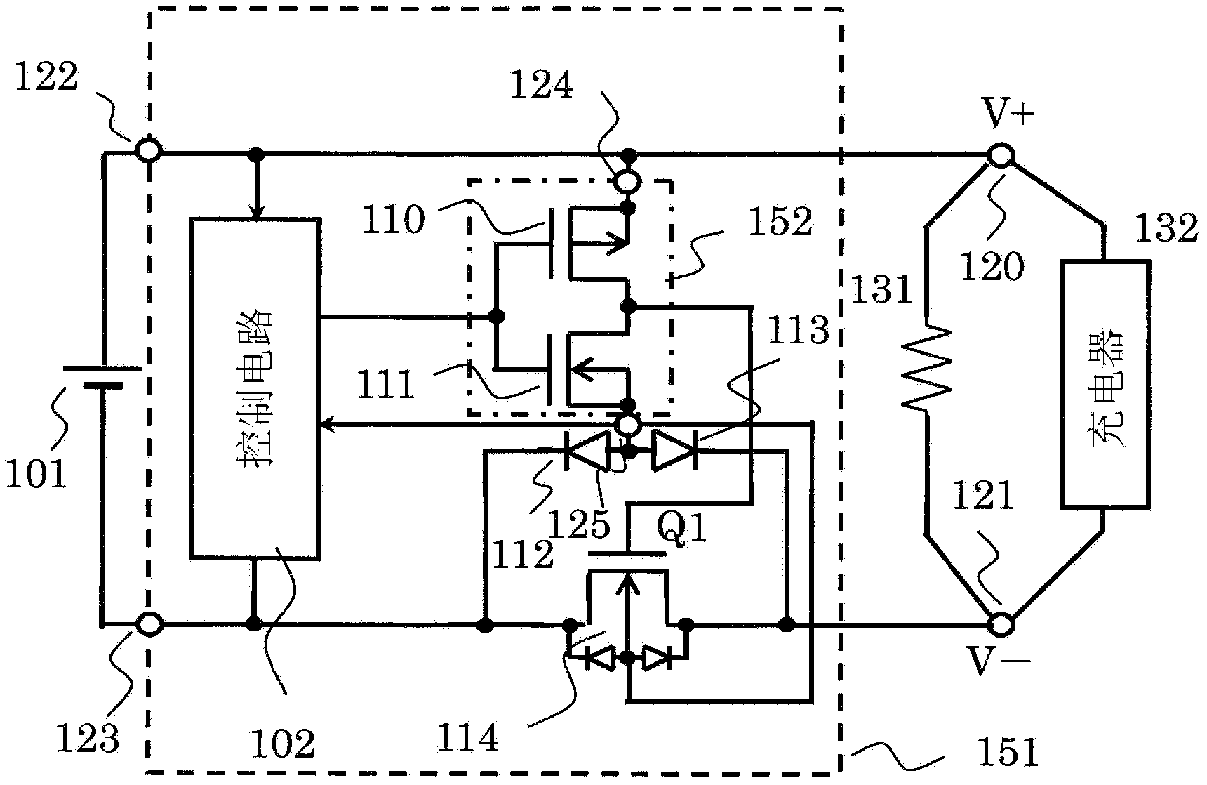
图1是第一实施方式的具有充放电控制电路的电池装置的电路图。FIG. 1 is a circuit diagram of a battery device having a charge and discharge control circuit according to a first embodiment.
图2是第二实施方式的具有充放电控制电路的电池装置的电路图。2 is a circuit diagram of a battery device having a charge and discharge control circuit according to a second embodiment.
图3是现有的具有充放电控制电路的电池装置的电路图。FIG. 3 is a circuit diagram of a conventional battery device having a charge and discharge control circuit.
标号说明Label description
101:二次电池;102:控制电路;151、251:充放电控制电路;152、252:开关电路;112、113、212、213:肖特基势垒二极管;114、214:双向导通型场效应晶体管;131:负载;132:充电器;302、303:二极管。101: secondary battery; 102: control circuit; 151, 251: charge and discharge control circuit; 152, 252: switch circuit; 112, 113, 212, 213: Schottky barrier diode; 114, 214: bidirectional conduction type Field effect transistor; 131: load; 132: charger; 302, 303: diode.
具体实施方式 Detailed ways
参照附图说明用于实施本发明的方式。Embodiments for implementing the present invention will be described with reference to the drawings.
【实施例1】【Example 1】
图1是第一实施方式的具有充放电控制电路151的电池装置的电路图。FIG. 1 is a circuit diagram of a battery device having a charge and
本实施方式的具有充放电控制电路151的电池装置具有二次电池101、控制电路102、双向导通型场效应晶体管114、连接有充电器132或负载131的外部端子120和121、肖特基势垒二极管112和113、PMOS晶体管110以及NMOS晶体管111。由PMOS晶体管110、NMOS晶体管111、端子124(第二端子)和端子125(第一端子)构成开关电路152。The battery device having the charge and
二次电池101的两端与正极电源端子122和负极电源端子123连接。控制电路102与正极电源端子122连接作为正极电源,与端子125连接作为负极电源,输出端与PMOS晶体管110的栅极和NMOS晶体管111的栅极连接。PMOS晶体管110的源极经由端子124与正极电源端子122和外部端子120连接,漏极与NMOS晶体管111的漏极连接。NMOS晶体管111的源极经由端子125与肖特基势垒二极管112的阳极和肖特基势垒二极管113的阳极连接,漏极与双向导通型场效应晶体管114的栅极连接,背栅与肖特基势垒二极管112的阳极和肖特基势垒二极管113的阳极连接。肖特基势垒二极管112的阴极与负极电源端子123连接,肖特基势垒二极管113的阴极与外部端子121连接。双向导通型场效应晶体管114的漏极与负极电源端子123连接,源极与外部端子121连接,背栅与端子125连接。Both ends of the
接着,对本实施方式的具有充放电控制电路151的电池装置的动作进行说明。Next, the operation of the battery device including the charge and
在外部端子120、121上连接有充电器132,通过控制电路102检测到二次电池101为可充放电状态时,控制电路102输出低电平,使PMOS晶体管110导通,使NMOS晶体管111截止。于是,双向导通型场效应晶体管114的栅电极与正极电源端子122连接从而成为导通状态。由此进行充放电。控制电路102的负极电源与端子125连接,因此能够输出负极电源端子123和外部端子121中较低一方的电压作为低电平。A
在外部端子120、121上连接有充电器132,通过控制电路102检测到二次电池变为充电禁止状态时,控制电路102输出高电平,使PMOS晶体管110截止,使NMOS晶体管111导通。于是,双向导通型场效应晶体管114的栅电极经由肖特基势垒二极管113、端子115、NMOS晶体管111被下拉至外部端子121,从而成为截止状态。由此,充电电流被截断,防止二次电池101被过充电。此外,肖特基势垒二极管112为反向偏置,防止电流从负极电源端子123流向外部端子121。在此,在本发明中采用VF电压较小(大约0.3V)的肖特基势垒二极管,因此能够减小双向导通型场效应晶体管114的栅极-源极间电压,能够减少截止漏电流。此外,双向导通型场效应晶体管114的背栅端子也不会浮动,因此能够使充放电控制电路151更稳定地动作。The
在外部端子120、121上连接有负载131,通过控制电路102检测到二次电池变为放电禁止状态时,控制电路102输出高电平,使PMOS晶体管110截止,使NMOS晶体管111导通。于是,双向导通型场效应晶体管114的栅电极经由肖特基势垒二极管112、端子115、NMOS晶体管111被下拉至负极电源端子123,从而成为截止状态。由此,放电电流被截断,防止二次电池101被过放电。此外,肖特基势垒二极管113为反向偏置,防止电流从外部端子121流向负极电源端子123。在此,在本发明中采用VF电压较小(大约0.3V)的肖特基势垒二极管,因此能够减小双向导通型场效应晶体管114的栅极-源极间电压,能够减少截止漏电流。此外,双向导通型场效应晶体管114的背栅端子也不会浮动,因此能够使充放电控制电路151更稳定地动作。A
如以上说明的那样,根据本实施方式的具有充放电控制电路151的电池装置,无论二次电池101变为充电禁止状态还是放电禁止状态,都能够减少流过双向导通型场效应晶体管114的漏电流。并且,能够通过控制双向导通型场效应晶体管114的背栅,使充放电控制电路151稳定地动作。As described above, according to the battery device including the charge-
另外,双向导通型场效应晶体管114也可以外装连接到充放电控制电路151。此外,虽然未图示,但是即使双向导通型场效应晶体管114的背栅端子不与端子125连接,也能够减少流过双向导通型场效应晶体管114的漏电流。In addition, the bidirectional conduction type
【实施例2】[Example 2]
图2是第二实施方式的具有充放电控制电路251的电池装置的电路图。FIG. 2 is a circuit diagram of a battery device having a charge and
第二实施方式的具有充放电控制电路251的电池装置具有二次电池101、控制电路102、双向导通型场效应晶体管214、连接有充电器132或负载131的外部端子120和121、肖特基势垒二极管212和213、PMOS晶体管210以及NMOS晶体管211。由PMOS晶体管210、NMOS晶体管211、端子124(第二端子)以及端子125(第一端子)构成开关电路252。The battery device having the charge and
二次电池101的两端与正极电源端子122和负极电源端子123连接。控制电路102与端子125连接作为正极电源,与负极电源端子123连接作为负极电源,输出端与PMOS晶体管210的栅极和NMOS晶体管211的栅极连接。PMOS晶体管210的源极和背栅经由端子125与肖特基势垒二极管212的阴极和肖特基势垒二极管213的阴极连接,漏极与NMOS晶体管211的漏极连接。NMOS晶体管211的源极经由端子124与负极电源端子123和外部端子121连接,漏极与双向导通型场效应晶体管114的栅极连接。肖特基势垒二极管212的阳极与正极电源端子122连接,肖特基势垒二极管213的阳极与外部端子120连接。双向导通型场效应晶体管214的漏极与正极电源端子122连接,源极与外部端子120连接,背栅与端子125连接。Both ends of the
接着,对第二实施方式的具有充放电控制电路251的电池装置的动作进行说明。Next, the operation of the battery device including the charge and
在外部端子120、121上连接有充电器132,通过控制电路102检测到二次电池101为可充放电状态时,控制电路102输出高电平,使PMOS晶体管210截止,使NMOS晶体管211导通。于是,双向导通型场效应晶体管214的栅电极与负极电源端子123连接从而成为导通状态。由此进行充放电。控制电路102的正极电源与端子125连接,因此能够输出正极电源端子122和外部端子120中较高一方的电压作为高电平。A
在外部端子120、121上连接有充电器132,通过控制电路102检测到二次电池101变为充电禁止状态时,控制电路102输出低电平,使PMOS晶体管210导通,使NMOS晶体管211截止。于是,双向导通型场效应晶体管214的栅电极经由肖特基势垒二极管213、端子115、PMOS晶体管210被上拉至外部端子120,从而成为截止状态。由此,充电电流被截断,防止二次电池101被过充电。此外,肖特基势垒二极管212为反向偏置,防止电流从外部端子120流向正极电源端子122。在此,在本发明中采用VF电压较小(大约0.3V)的肖特基势垒二极管,因此能够减小双向导通型场效应晶体管214的栅极-源极间电压,能够减少截止漏电流。此外,双向导通型场效应晶体管214的背栅端子也不会浮动,因此能够使充放电控制电路251更稳定地动作。A
在外部端子120、121上连接有负载131,通过控制电路102检测到二次电池变为放电禁止状态时,控制电路102输出低电平,使PMOS晶体管210导通,使NMOS晶体管211截止。于是,双向导通型场效应晶体管214的栅电极和背栅经由肖特基势垒二极管212、端子125、PMOS晶体管210被上拉至正极电源端子122,从而成为截止状态。由此,放电电流被截断,防止二次电池101被过放电。此外,肖特基势垒二极管213为反向偏置,防止电流从正极电源端子122流向外部端子120。在此,在本发明中采用VF电压较小(大约0.3V)的肖特基势垒二极管,因此能够减小双向导通型场效应晶体管214的栅极-源极间电压,能够减少截止漏电流。此外,双向导通型场效应晶体管214的背栅端子也不会浮动,因此能够使充放电控制电路251更稳定地动作。The
如以上说明的那样,根据第二实施方式的具有充放电控制电路251的电池装置,无论二次电池101变为充电禁止状态还是放电禁止状态,都能够减少流过双向导通型场效应晶体管214的漏电流。并且,能够通过控制双向导通型场效应晶体管214的背栅,使充放电控制电路251稳定地动作。As described above, according to the battery device having the charge and
另外,双向导通型场效应晶体管214也可以外装连接到充放电控制电路251。此外,虽然未图示,但是即使双向导通型场效应晶体管214的背栅端子不与端子125连接,也能够减少流过双向导通型场效应晶体管214的漏电流。In addition, the bidirectional conduction type
Claims (8)
Applications Claiming Priority (2)
| Application Number | Priority Date | Filing Date | Title |
|---|---|---|---|
| JP2010201122A JP2012060762A (en) | 2010-09-08 | 2010-09-08 | Charge and discharge control circuit, and battery device |
| JP2010-201122 | 2010-09-08 |
Publications (1)
| Publication Number | Publication Date |
|---|---|
| CN102403756A true CN102403756A (en) | 2012-04-04 |
Family
ID=45770222
Family Applications (1)
| Application Number | Title | Priority Date | Filing Date |
|---|---|---|---|
| CN2011102635231A Pending CN102403756A (en) | 2010-09-08 | 2011-09-07 | Charge/discharge control circuit and battery device |
Country Status (5)
| Country | Link |
|---|---|
| US (1) | US20120056593A1 (en) |
| JP (1) | JP2012060762A (en) |
| KR (1) | KR20120025993A (en) |
| CN (1) | CN102403756A (en) |
| TW (1) | TW201240269A (en) |
Cited By (7)
| Publication number | Priority date | Publication date | Assignee | Title |
|---|---|---|---|---|
| CN106026244A (en) * | 2016-06-12 | 2016-10-12 | 深圳市德朗能电子科技有限公司 | Lithium ion battery charge and discharge protective circuit and lithium ion battery system |
| CN106067684A (en) * | 2015-04-21 | 2016-11-02 | 精工半导体有限公司 | Cell apparatus |
| CN106851952A (en) * | 2017-01-04 | 2017-06-13 | 上海奕瑞光电子科技有限公司 | A kind of flat panel detector circuit implementing method for reducing patient leakage current |
| CN107611936A (en) * | 2016-07-11 | 2018-01-19 | 三美电机株式会社 | Secondary battery protection circuit |
| CN107925255A (en) * | 2015-08-20 | 2018-04-17 | Itm半导体有限公司 | Battery protecting circuit module and the battery pack including the module |
| CN114050629A (en) * | 2021-11-30 | 2022-02-15 | 深圳天狼芯半导体有限公司 | Charge-discharge control circuit and battery protection device |
| CN117223189A (en) * | 2021-04-30 | 2023-12-12 | 罗伯特·博世有限公司 | A method and a circuit arrangement for a control device |
Families Citing this family (9)
| Publication number | Priority date | Publication date | Assignee | Title |
|---|---|---|---|---|
| CN104076893A (en) * | 2013-03-27 | 2014-10-01 | 鸿富锦精密电子(天津)有限公司 | Computer and charging circuit of computer |
| CN104076894A (en) * | 2013-03-28 | 2014-10-01 | 鸿富锦精密电子(天津)有限公司 | Computer and charging circuit of computer |
| KR20150008227A (en) * | 2013-07-11 | 2015-01-22 | 주식회사 아이티엠반도체 | Battery protection circuit and IC system using single MOSFET |
| CN104348225B (en) * | 2014-08-12 | 2017-07-11 | 矽力杰半导体技术(杭州)有限公司 | A kind of battery charge-discharge circuit of Single switch and the control method of battery charging and discharging |
| KR101784740B1 (en) | 2016-02-25 | 2017-11-06 | 삼성에스디아이 주식회사 | Battery protection circuit and battery pack including same |
| JP6577916B2 (en) * | 2016-07-11 | 2019-09-18 | ミツミ電機株式会社 | Protection IC |
| CN109995116A (en) * | 2019-04-23 | 2019-07-09 | 北斗航天汽车(北京)有限公司 | Battery inexpensive automatic inflatable electric control circuit and control method |
| US11349316B2 (en) * | 2020-04-20 | 2022-05-31 | The Boeing Company | System and method for controlling a high-voltage battery system |
| CN115811104A (en) * | 2021-09-14 | 2023-03-17 | 艾普凌科株式会社 | Cell balancing circuit and device, charge and discharge control circuit and device and battery device |
Citations (4)
| Publication number | Priority date | Publication date | Assignee | Title |
|---|---|---|---|---|
| CN1327288A (en) * | 2000-06-02 | 2001-12-19 | 精工电子有限公司 | Charging/discharging type power source |
| CN1153325C (en) * | 1997-02-04 | 2004-06-09 | 精工电子有限公司 | Charging and discharging control circuit |
| CN1909325A (en) * | 2005-08-01 | 2007-02-07 | 三洋电机株式会社 | Battery pack with circuit protection function |
| JP2008079354A (en) * | 2006-09-19 | 2008-04-03 | Ricoh Co Ltd | Back gate voltage generation circuit, four-terminal back gate switching FET, charge / discharge protection circuit using the FET, battery pack incorporating the charge / discharge protection circuit, and electronic device using the battery pack |
Family Cites Families (14)
| Publication number | Priority date | Publication date | Assignee | Title |
|---|---|---|---|---|
| JP2000102182A (en) * | 1998-09-29 | 2000-04-07 | Hitachi Ltd | Overcharge / overdischarge prevention circuit for secondary battery |
| EP1320168A1 (en) * | 2001-12-12 | 2003-06-18 | Dialog Semiconductor GmbH | Power switch for battery protection |
| US7528582B1 (en) * | 2003-01-21 | 2009-05-05 | Microsemi Corp. | Battery charging and discharging by using a bi-directional transistor |
| TWM248123U (en) * | 2003-12-02 | 2004-10-21 | Chin Hsen Technology Corp | Improved structure of charging battery circuit |
| KR100568255B1 (en) * | 2004-01-26 | 2006-04-07 | 삼성전자주식회사 | Bidirectional high voltage switching device and energy recovery circuit including the same |
| JP4785411B2 (en) * | 2004-07-16 | 2011-10-05 | セイコーインスツル株式会社 | Charge pump circuit |
| US7154291B2 (en) * | 2004-08-24 | 2006-12-26 | Delphi Technologies, Inc. | Measuring bi-directional current through a field-effect transistor by virtue of drain-to-source voltage measurement |
| JP2006108568A (en) * | 2004-10-08 | 2006-04-20 | Sanyo Electric Co Ltd | Switching element and protection circuit using the same |
| JP4522384B2 (en) * | 2005-08-01 | 2010-08-11 | 三洋電機株式会社 | Battery pack with protection circuit |
| JP5050415B2 (en) * | 2006-06-15 | 2012-10-17 | ミツミ電機株式会社 | Secondary battery charge / discharge circuit and battery pack |
| JP4844468B2 (en) * | 2007-05-08 | 2011-12-28 | 富士電機株式会社 | Secondary battery protection device and semiconductor integrated circuit device |
| KR100938080B1 (en) * | 2007-09-28 | 2010-01-21 | 삼성에스디아이 주식회사 | Safety circuit and battery pack using same |
| JP5439800B2 (en) * | 2008-12-04 | 2014-03-12 | ミツミ電機株式会社 | Secondary battery protection integrated circuit device, secondary battery protection module using the same, and battery pack |
| US7999512B2 (en) * | 2008-12-16 | 2011-08-16 | Hong Kong Applied Science & Technology Research Institute Company, Ltd. | Single-power-transistor battery-charging circuit using voltage-boosted clock |
-
2010
- 2010-09-08 JP JP2010201122A patent/JP2012060762A/en not_active Withdrawn
-
2011
- 2011-08-15 US US13/209,671 patent/US20120056593A1/en not_active Abandoned
- 2011-08-18 TW TW100129531A patent/TW201240269A/en unknown
- 2011-09-06 KR KR1020110090144A patent/KR20120025993A/en not_active Withdrawn
- 2011-09-07 CN CN2011102635231A patent/CN102403756A/en active Pending
Patent Citations (4)
| Publication number | Priority date | Publication date | Assignee | Title |
|---|---|---|---|---|
| CN1153325C (en) * | 1997-02-04 | 2004-06-09 | 精工电子有限公司 | Charging and discharging control circuit |
| CN1327288A (en) * | 2000-06-02 | 2001-12-19 | 精工电子有限公司 | Charging/discharging type power source |
| CN1909325A (en) * | 2005-08-01 | 2007-02-07 | 三洋电机株式会社 | Battery pack with circuit protection function |
| JP2008079354A (en) * | 2006-09-19 | 2008-04-03 | Ricoh Co Ltd | Back gate voltage generation circuit, four-terminal back gate switching FET, charge / discharge protection circuit using the FET, battery pack incorporating the charge / discharge protection circuit, and electronic device using the battery pack |
Cited By (12)
| Publication number | Priority date | Publication date | Assignee | Title |
|---|---|---|---|---|
| CN106067684A (en) * | 2015-04-21 | 2016-11-02 | 精工半导体有限公司 | Cell apparatus |
| CN106067684B (en) * | 2015-04-21 | 2020-01-21 | 艾普凌科有限公司 | battery unit |
| CN107925255A (en) * | 2015-08-20 | 2018-04-17 | Itm半导体有限公司 | Battery protecting circuit module and the battery pack including the module |
| CN107925255B (en) * | 2015-08-20 | 2021-05-25 | Itm半导体有限公司 | Battery protection circuit module and battery pack including the same |
| CN106026244A (en) * | 2016-06-12 | 2016-10-12 | 深圳市德朗能电子科技有限公司 | Lithium ion battery charge and discharge protective circuit and lithium ion battery system |
| CN106026244B (en) * | 2016-06-12 | 2019-03-12 | 深圳市德朗能电子科技有限公司 | Lithium ion battery charge-discharge protection circuit and lithium-ion battery systems |
| CN107611936A (en) * | 2016-07-11 | 2018-01-19 | 三美电机株式会社 | Secondary battery protection circuit |
| CN107611936B (en) * | 2016-07-11 | 2019-06-07 | 三美电机株式会社 | Secondary battery protection circuit |
| CN106851952A (en) * | 2017-01-04 | 2017-06-13 | 上海奕瑞光电子科技有限公司 | A kind of flat panel detector circuit implementing method for reducing patient leakage current |
| CN106851952B (en) * | 2017-01-04 | 2018-09-25 | 上海奕瑞光电子科技股份有限公司 | A kind of flat panel detector circuit implementing method reducing patient leakage current |
| CN117223189A (en) * | 2021-04-30 | 2023-12-12 | 罗伯特·博世有限公司 | A method and a circuit arrangement for a control device |
| CN114050629A (en) * | 2021-11-30 | 2022-02-15 | 深圳天狼芯半导体有限公司 | Charge-discharge control circuit and battery protection device |
Also Published As
| Publication number | Publication date |
|---|---|
| JP2012060762A (en) | 2012-03-22 |
| US20120056593A1 (en) | 2012-03-08 |
| KR20120025993A (en) | 2012-03-16 |
| TW201240269A (en) | 2012-10-01 |
Similar Documents
| Publication | Publication Date | Title |
|---|---|---|
| CN102403757B (en) | Charge-discharge control circuit and cell apparatus | |
| JP6614388B1 (en) | Secondary battery protection circuit, secondary battery protection device, battery pack, and control method of secondary battery protection circuit | |
| US20120056593A1 (en) | Charge/discharge control circuit and battery device | |
| CN101055999B (en) | Charge/discharge protection circuit and power-supply unit | |
| KR102147864B1 (en) | Protection ic and semiconductor integrated circuit | |
| US9214821B2 (en) | Charge/discharge control circuit and battery device | |
| CN102904218B (en) | Battery protection ic and cell apparatus | |
| US10498149B2 (en) | Rechargeable battery protection integrated circuit, rechargeable battery protection device, and battery pack | |
| US9401615B2 (en) | Charging and discharging control circuit and battery device | |
| CN102738775A (en) | Battery protection circuit, battery protection device, and battery pack | |
| CN107611936A (en) | Secondary battery protection circuit | |
| CN102403758B (en) | Charge-discharge control circuit and cell apparatus | |
| TWI287874B (en) | Switching element and protection circuit using the same | |
| KR20050057693A (en) | Charge-discharge protect circuit | |
| CN115800424A (en) | Battery protection chip and system with positive terminal charging and discharging |
Legal Events
| Date | Code | Title | Description |
|---|---|---|---|
| C06 | Publication | ||
| PB01 | Publication | ||
| C10 | Entry into substantive examination | ||
| SE01 | Entry into force of request for substantive examination | ||
| C02 | Deemed withdrawal of patent application after publication (patent law 2001) | ||
| WD01 | Invention patent application deemed withdrawn after publication |
Application publication date: 20120404 |