This application is based on and claims priority from prior japanese patent application No. 2011-.
Detailed Description
Hereinafter, embodiments will be described with reference to the accompanying drawings.
A photoelectric conversion element according to an embodiment will be described with reference to the drawings. Wherever possible, the same reference numbers will be used throughout the drawings to refer to the same or like parts.
First, the principle of long wavelength absorption will be described with reference to fig. 1 and 2. The principle of long-wavelength absorption is due to impurity levels in the band gap of the photoelectric conversion layer of the photoelectric conversion element according to the embodiment. Fig. 1 is a graph showing the solar spectrum (AM1.5, air mass 1.5 as solar spectral irradiance) of the photoelectric conversion element of the background art. Fig. 2 is a graph showing spectral sensitivity characteristics of a single crystalline silicon solar cell of a photoelectric conversion element according to the background art. The horizontal axis and the vertical axis of fig. 1 represent the wavelength and spectral sensitivity characteristics of light, respectively. In addition, the horizontal axis and the vertical axis of fig. 2 represent the wavelength and the quantum efficiency of light, respectively.
As shown in fig. 1, the solar spectrum is based on the black body radiation of the sun. Therefore, the wavelength of the radiated light is in a wide range of 300 nm to 2500 nm, i.e., a long wavelength.
On the other hand, as shown in fig. 2, the light absorption spectrum of single crystal silicon is determined by the band gap of silicon, i.e., 1.12 eV. Thus, it should be noted that light can only be absorbed within a narrow range of 300-. For this reason, the light absorption current is generated from only a part of sunlight in the photoelectric conversion element of the background art. As a result, the photoelectric conversion element of the background art has a low power generation efficiency of 20%.
Here, in general, a semiconductor having a narrow band gap, such as germanium, seems to be advantageous for use in a photoelectric conversion element in a longer wavelength range. However, the narrow band gap expands the wavelength range of light to be absorbed while lowering the open circuit voltage of the photoelectric conversion element, resulting in no increase in the power generation efficiency thereof. In fact, the power generation efficiency is reduced due to the low open circuit voltage.
Therefore, the photoelectric conversion element must absorb light in the long wavelength range while maintaining a specific band gap (1-2 eV).
As a result, the inventors found that the impurity levels formed in the band gap absorb light of a long wavelength. Specifically, light is absorbed by impurity levels in the bandgap to generate electrons and holes. If electrons (holes) are thermally excited to the conduction band (valence band) at room temperature, the electrons (holes) can be taken out as a photocurrent.
Fig. 3 is a schematic diagram showing band gap levels of the photoelectric conversion element according to the embodiment.
Fig. 3 shows that if the band gap difference Δ E between the impurity level and the conduction band (valence band) is 0.1eV, an electron (hole) is taken out to the conduction band (valence band) by thermal excitation, allowing it to absorb light. However, the impurity level having such a difference in band gap of 0.1eV is not necessarily formed. Alternatively, the impurity level may be formed to just generate a band gap difference between the impurity level and the conduction band (valence band) if the band gap difference allows electrons (holes) to be excited from the impurity level to the conduction band (valence band) and taken out.
Fig. 4 is a table showing Δ E and a thermal excitation ratio exp (Δ E/RT) at room temperature of the photoelectric conversion element according to the embodiment.
As shown in fig. 4, a small Δ E increases the thermal excitation ratio exp (Δ E/RT) from the impurity level to the conduction band (valence band), allowing it to extract electrons (holes) as a photocurrent. On the other hand, a large Δ E reduces the thermal excitation ratio, making it difficult to extract electrons (holes) as a photocurrent. Therefore, Δ E is not preferably too large, but Δ E is preferably less than 0.1 eV.
Further, fig. 5 is a graph showing a solar spectrum of the photoelectric conversion element according to the embodiment.
Fig. 5 shows that the light absorption region extends to a long wavelength region of about 100 nm in the solar spectrum if the band gap Eg of silicon is 1.12eV and Δ E is 0.1 eV.
Here, the impurities used for the impurity level of silicon include S, In, Se, and S — O. The impurities used for the impurity level in the compound semiconductor include Be, Cu, Li, Tl, Zn, Cd, O, Zn-O. However, in silicon or a compound semiconductor, impurities are not limited to the above.
In addition, several combinations of dopants for electrons and holes (e.g., Ga, Al, Mg) allow light to be absorbed in the long wavelength range not less than the band gap.
The structure of the photoelectric conversion element according to the embodiment will be described with reference to fig. 6A to 7B. Fig. 6A is a schematic view showing the structure of a photoelectric conversion element of the related art. Fig. 6B is a graph showing the relationship between the wavelength of light and the quantum efficiency of the photoelectric conversion element of the background art. Fig. 7A is a schematic diagram illustrating a structure of a photoelectric conversion element having a long wavelength absorption layer according to the embodiment. Fig. 7B is a graph showing the relationship between the wavelength of light and the quantum efficiency of the structure of the photoelectric conversion element having a long-wavelength absorption layer according to the embodiment.
As shown in fig. 6A, in the photoelectric conversion element of the related art, an n + layer 2 is laminated on a p-type silicon layer 1, and a front electrode 4 (first metal layer) is provided on the surface of the n + layer 2. Further, a rear electrode 3 is provided on the rear surface of the p-type silicon layer 1. In the photoelectric conversion element of the related art, when external light is incident on the p-type silicon layer 1, electrons and holes are separated into a conduction band and a valence band according to an energy level in a band gap, and taken out as a photocurrent to an external power supply Voc.
Fig. 6B shows that light of a long wavelength reduces the quantum efficiency of the photoelectric conversion element of the background art. Therefore, the long-wavelength light lowers the quantum efficiency, making it impossible to take out the photocurrent to the outside.
As shown in fig. 7A, in the photoelectric conversion element having a long wavelength absorption layer according to the embodiment, in the same manner as in fig. 6A, an n + layer 2 is laminated on a p-type silicon layer 1, and a front electrode 4 (first metal layer) is provided on the n + layer 2. Further, a rear electrode 3 is provided on the rear surface of the p-type silicon layer 1. Further, the long wavelength absorption layer 5 is disposed on the rear surface of the p-type silicon layer 1 so as not to contact the rear electrode 3. The long wavelength absorption layer 5 is doped with impurities from the rear surface of the p-type silicon layer 1. Here, the photoelectric conversion element having the long wavelength absorption layer 5 can provide a voltage of 1.12eV corresponding to the band gap.
In this case, as shown in fig. 7B, the photoelectric conversion element according to the embodiment has the long wavelength absorption layer 5 to absorb light longer than the wavelength shown in fig. 6B. Thus, additional absorption regions occur in the longer wavelength range (indicated by the dashed line in fig. 7B).
However, the quantum efficiency of the absorption region is smaller in a longer wavelength range as shown by the dotted line of fig. 7B. This can be understood as follows. The doping concentration in the long wavelength absorption layer 5 is at most from 1 × 10²⁰Centimeter-3To 1X 10²¹Centimeter-3Within the range of (1). As a result, the absorption coefficient of light is large, and the amount of light absorption per unit volume becomes small, thereby lowering the actual spectral sensitivity.
Therefore, a method of increasing the light absorption amount per unit volume is required for the photoelectric conversion element having the long wavelength absorption layer according to the embodiment.
The present inventors have found that the following structure of the photoelectric conversion element contributes to the amount of light absorption. In this structure, an enhanced electric field is generated by plasmon resonance due to the metal nanostructure, thereby increasing carrier excitation. Carrier excitation produces an enhanced electric field several to several hundred times the normal electric field at a depth of several tens of nanometers immediately below the metal nanostructures. With the metal nanostructure having such an electric field enhancement effect, the enhanced electric field contributes to the amount of light absorption. The photoelectric conversion element having the above-described structure enables a significant increase in the light absorption amount of the long wavelength absorption layer 5.
Fig. 8A is a schematic view illustrating a structure of a photoelectric conversion element having a long wavelength absorption layer and a nano mesh electrode according to the embodiment. Fig. 8B is a graph showing a relationship between the wavelength of light and the quantum efficiency of the photoelectric conversion element according to the embodiment having the long wavelength absorption layer and the nano mesh electrode.
As shown in fig. 8A, in the photoelectric conversion element having the long wavelength absorption layer and the nano mesh electrode according to the embodiment, in the same manner as in fig. 7A, the n + layer 2 is laminated on the p-type silicon layer 1, and the front electrode 4 (first metal layer) is provided to the surface of the n + layer 2. Further, a rear electrode 3 is provided to the rear surface of the p-type silicon layer 1. Further, the long wavelength absorption layer 5 is provided to the rear surface of the p-type silicon layer 1 such that the long wavelength absorption layer 5 does not contact the rear electrode 3. The long wavelength absorption layer 5 is doped with impurities from the rear surface of the p-type silicon layer 1. The nano mesh electrode 6 is disposed between the rear electrodes 3 such that the nano mesh electrode 6 contacts the long wavelength absorption layer 5. The nano mesh electrode 6 forms a metal microstructure on the long wavelength absorption layer 5.
Here, as shown in fig. 8A, in the same manner as in fig. 7A, the photoelectric conversion element of this embodiment has the long wavelength absorption layer 5 and the nano mesh electrode 6 so that the long wavelength absorption layer 5 does not contact the rear electrode 3, thereby allowing a voltage corresponding to the band gap of the long wavelength absorption layer 5 to be obtained. The long wavelength absorption layer 5 also adds an additional absorption region (dotted line in fig. 8B) on the long wavelength side of fig. 8B. Further, the long wavelength absorption layer 5 has the nano mesh electrode 6 thereon to increase the light absorption amount due to the enhancement effect of the electric field. As shown by the thick dotted line in fig. 8B, an increase in the amount of light absorption improves the quantum efficiency.
In addition, when the long wavelength absorption layer 5 is doped with an excessive amount of impurities (more than 1 × 10)22Centimeter-3) When the solid state properties (including band gap) of the semiconductor itself, i.e., the substrate, are completely changed. The excessive impurities prevent the formation of a long wavelength absorption region (indicated by a dotted line in fig. 7 and 8B).
And, the intensity of the enhanced electric field generated by the nano mesh electrode 6 is several to several hundred times its normal intensity. In this case, the low doping amount of impurities in the long wavelength absorption layer 5 reduces the absorption amount in the long wavelength region. Therefore, the absorption amount therein is preferably about 1X 10¹⁹Centimeter-3。
Further, the long wavelength absorption layer 5 needs to be disposed in the vicinity of the nano mesh electrode 6. This is because the enhanced electric field due to the nano mesh electrode 6 is generated within a depth of 10 nm immediately below the nano mesh electrode 6, and the enhanced electric field peaks immediately below the nano mesh electrode 6. Therefore, the long wavelength absorption layer 5 is preferably disposed within a depth of 5 nm from the nano mesh electrode 6 so that the long wavelength absorption layer 5 benefits from the enhanced electric field.
The range of electric field enhancement due to the nano-mesh electrode 6 is in the range of several tens of nanometers immediately below the nano-mesh electrode 6 and peaks directly below the nano-mesh electrode 6, allowing the long wavelength absorption layer 5 having a thickness of 10 nanometers to benefit from electric field enhancement.
Further, the long wavelength absorption layer 5 is doped with impurities to allow up to about 1 × 10 at a depth of about 1000 nm from the surface thereof19Centimeter-3High concentration of (2). However, the electric field enhancement is in the range of tens of nanometers immediately below the nano-mesh electrode 6. Thus, 1000 nm is a sufficient thickness for the long wavelength absorbing layer 5.
As described above, the photoelectric conversion element according to the embodiment as shown in fig. 8A is provided with the long-wavelength absorption layer 5 and the nano mesh electrode 6, thereby providing a power generation efficiency higher than that of the photoelectric conversion element of the related art.
Next, a principle of generating an enhanced electric field using plasmon resonance due to the metal nanostructure will be described with reference to fig. 9A and 9B. Fig. 9A and 9B are schematic views respectively showing the movement of free electrons and the generation of a local electric field in the case where a metal nanostructure is irradiated with light.
Fig. 9A shows that the metal nanostructure 10 has a size equivalent to or smaller than the wavelength of the light 12 and is irradiated with the light 12. Such fine metallic nanostructures 10 irradiated with light are known to excite surface plasmons therein. When the metal nanostructure 10 is irradiated by light 12, free electrons 11 vibrate in the metal nanostructure 10 perpendicular to the traveling direction of the light 12. At this time, dense portions and sparse portions are generated on the upper surface (the side irradiated with the light 12) of the metal nanostructure 10 due to the vibration of free electrons. The dense portion includes dense free electrons. The sparse portion includes sparse free electrons.
As shown in fig. 9B, the local electric field 15 is excited in the vicinity of the metal nanostructure 10 to vibrate parallel to the traveling direction of the light 12. The local electric field 15 excited at this time has a strength as high as several hundred times that of the electric field generated by the light 12 to enhance the excitation of electron-hole pairs.
Here, the metal nanostructure including the nano mesh electrode 6 and the dot metal 7 will be described with reference to fig. 10A and 10B. Fig. 10A is a perspective view showing the nano mesh electrode 6. Fig. 10B is a perspective view showing the dot-shaped metal 7.
The porous film may be used as a metal nanostructure, for example, nano-mesh metal 6. In the porous membrane structure, two or more openings (through holes) are provided to the continuous metal membrane, as shown in fig. 10A. The opening has a size comparable to the wavelength of the incident light.
Alternatively, in the porous film structure used as the metal nanostructure, two or more dot-shaped metals 7 are formed on the p-type silicon layer 1, as shown in fig. 10B. The metal dots have a diameter r corresponding to the wavelength of the incident light and are arranged at regular distances l.
Next, the case of a strong local electric field excited by the metal nanostructure will be described with reference to fig. 11A and 11B.
Fig. 11A is a schematic of a metal nanostructure. Fig. 11B is a simulation diagram illustrating a metal nanostructure by a Finite Difference Time Domain (FDTD) method.
As shown in fig. 11A, if the thickness of Al21 is 30 nm and an opening 23 (through-hole) is prepared in Al21, a structure of Si20/Al (aluminum) 21/air 22 is formed. The openings 23 of Al21 have a diameter of 100 nm and a spacing i of 200 nm.
Fig. 11B is a simulation diagram showing an electric field intensity when the incident light 24(λ 1000 nm, traveling direction) is incident on the structure of fig. 11A by a Finite Difference Time Domain (FDTD) method. The simulation shows that the electric field is enhanced near the end of Al21, creating a local electric field 25.
Further, the nano mesh electrode 6, i.e., the relationship between the opening interval of the metal nanostructure and the electric field enhancement, will be described with reference to fig. 12. Fig. 12 is a graph showing the relationship between the opening interval of the nano mesh electrode 6 and the electric field enhancement. The vertical axis and the horizontal axis represent the electric field intensity and the opening interval of the nano-mesh electrode 6, respectively.
As shown in fig. 12, in a region where the wavelength of light is not less than about 1000 nm, the pitch l of the openings (via holes) 23 may be not more than 1 μm in order to generate electric field enhancement for the end of Al 21. When the pitch i is converted into the area of each opening 23, the area may be not more than 0.8 square micrometers. Further, the working accuracy of the pitch l of the openings 23 and the pitch l of the openings 23 may be about several tens of nanometers. When converted to the area of each opening 23, the area may be not less than 80 square nanometers.
Further, the above simulation shows the following. When the film thickness of Al21 is not less than 2 nm, electric field enhancement can be sufficiently generated. In addition, when the film thickness of Al21 is thicker than 200 nm, the electric field enhancement saturates.
Also, simulation has been performed on the dot-like metal 7, i.e., the metal nanostructure, in the same manner as on the nano mesh electrode 6. Fig. 13 is a graph showing the relationship between the radius of the dotted metal 7 and the range of the local electric field. The vertical axis and the horizontal axis represent the range of the local electric field immediately below the dot-shaped metal 7 and the radius of the dot-shaped metal 7, respectively.
As shown in fig. 13, the radius of the dot-shaped metal 7 is in the range of 1 nm to 1000 nm. When the dot-shaped metal 7 assumes a spherical shape, the range corresponds to the dot-shaped metal 7 having a volume of not less than 4 cubic nanometers and not more than 0.52 cubic micrometers. A point-like metal having such a volume can produce a high electric field enhancement effect.
The following situation has been elucidated. When electric field enhancement is being generated in the range of 1000 nm or more, electric energy moves to an excessively narrow space between the dot-like metals 7, thereby reducing the electric field enhancement effect.
As shown in FIG. 13, the small size of the dot-shaped metal 7 will limit the range of the local electric fieldTo about half its size. In particular, a punctiform metal 7 (volume 4 cubic nanometers) with a radius of 1 nanometer provides a local electric field in the range of 1 nanometer (approximately equal to the radius). However, the large size of the dot-shaped metal 7 does not necessarily provide a large range of local electric fields. The dot-shaped metal 7 having a radius larger than a certain length may provide a local electric field of only a range of 100 nm or less. Specifically, a dot-shaped metal 7 (volume 4 × 10) having a radius of 10 nm or more-3Cubic microns) provides a local electric field in the range of about 100 nanometers or less.
Therefore, when the point metal has a size of less than 4 × 10⁻³When the volume is cubic micrometers and the distance between two dot-shaped metals 7 adjacent to each other is 1 nm or more, energy transfer does not occur between the two dot-shaped metals 7.
When the point metal has a size larger than 4 x 10⁻³When the volume is cubic micrometers and the distance between two dot-shaped metals 7 adjacent to each other is 100 nanometers or more, energy transfer does not occur between the two dot-shaped metals 7.
However, when the distance between two dot metals 7 is too long, the occupancy ratio of the dot metals 7 is lowered to weaken the electric field enhancement, resulting in a preferable distance of not more than 1 μm between two dot metals 7 adjacent to each other.
Next, the case of carriers generated from the long wavelength absorption layer 5 will be described below.
As shown in fig. 7A, carriers, i.e., electrons generated from the long wavelength absorption layer 5 diffuse through the P-type layer (P-type silicon substrate) and need to reach a depletion layer (not shown) near the n + layer 2 on the surface of the P-type silicon layer 1. Therefore, the lifetime of carriers must be very long or the p-type silicon layer 1 must be made thin.
Thinning the p-type silicon layer 1 may reduce the quantum efficiency at the absorption wavelength of silicon, producing undesirable results. When the carriers themselves have a long lifetime, the carriers, i.e., generated electrons, completely diffuse through the p-type silicon layer 1 and can reach a depletion layer near the n + layer 2 on the surface of the p-type silicon layer 1. Therefore, such a long lifetime of carriers can maintain quantum efficiency.
In contrast, some difficulties such as short lifetime of carriers prevent carriers from completely diffusing through the p-type silicon layer 1 to reach a depletion layer near the n + layer 2 on the surface of the p-type silicon layer 1, thereby creating a risk of a decrease in quantum efficiency. Therefore, the preferred embodiment employs an n-type layer having a polarity opposite to that of the p-type silicon layer 1 as the long wavelength absorption layer 5.
Such a configuration forms a p-n junction to create a built-in potential between the n-type long wavelength absorbing layer 5 and the p-type silicon layer 1. Minority carriers, i.e., holes, are generated in the long wavelength absorption layer 5 as an n-type layer. When the holes reach the depletion layer at the p-n junction comprising the n-type long wavelength absorption layer 5 and the p-type silicon layer 1, the built-in potential brings the holes into the p-type silicon layer 1 (substrate).
The long wavelength absorption layer 5, i.e., the n-type layer, is as thin as several micrometers or less, thereby allowing holes to easily reach the rear electrode. Therefore, it is not necessary to thin the substrate or care about the lifetime of carriers. This makes it possible to efficiently take out the photocurrent generated in the long wavelength absorption layer 5.
The elements including P, Sb, and B can be used to make the long wavelength absorption layer 5 an n-type layer having a polarity opposite to that of the P-type silicon layer 1 which is the photoelectric conversion layer.
An exemplary manufacturing method of a photoelectric conversion element according to the embodiment will be described with reference to fig. 14A to 16D. Fig. 14A to 16D are sectional views showing manufacturing steps of a photoelectric conversion element according to the embodiment.
In addition, in order to form a metal electrode pattern having an opening of not more than 200 nm to 300 nm, it is necessary to use the latest exposure system and EB lithography system for manufacturing a semiconductor integrated circuit. However, large area and cost reduction cannot be achieved with advanced exposure systems and EB lithography systems. Nanoimprinting is one of the promising methods for achieving large areas and cost reductions. A method of producing the nano net-shaped metal (metal thin film) will be described.
As shown in fig. 14A, having a size of 1 × 10¹⁶Centimeter-3The p-type silicon single crystal substrate 30 of doping concentration is prepared as a substrate, and then a silicon dioxide film 31 having a thickness of 150 nm is formed by thermally oxidizing the surface of the p-type silicon single crystal substrate 30.
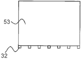
As shown in fig. 14B, the silicon oxide film 31 was patterned into a grid-shaped pattern having a width of 100 μm and a pitch of 1 mm by using a photolithography method.
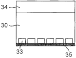
Further, as shown in fig. 14C, using the silicon dioxide mask 32 as a mask, S (sulfur) ions are implanted to form a long wavelength absorption layer 33.
As shown in fig. 14D, the silicon dioxide mask 32 is removed, and then activation annealing is performed on the implanted S to form a long wavelength absorption layer 33. Doping the long wavelength absorbing layer 33 with S to 1 × 10 within 100 nm from the silicon surface20Centimeter-3The concentration of (c).
As shown in fig. 14E, P (phosphorus) ions are implanted at the opposite side to that which has been doped with S. Then, P ions are implanted and activation annealing is performed to provide n + layer 34 with a thickness of 1X 10 nm within 200 nm from the silicon surface20Centimeter-3The concentration of (c).
As shown in fig. 14F, an Ag layer having a thickness of 30 nm was formed on the side that had been doped with S by a deposition method, thereby providing an Ag layer 35.
Further, as shown in fig. 15A, a resist 36 is formed on the Ag layer 35 formed on the rear surface of the p-type silicon single crystal substrate 30.
As shown in fig. 15B, the imprint is performed as follows. The quartz stamper 37 is pressed to the resist 36 with the p-type silicon single crystal substrate 30 heated, so that the surface of the quartz stamper 37 having a convex shape contacts the resist 36. The quartz stamper 37 was provided with a convex shape having a size of 200 nm (the shape was formed to have an area of 9 square centimeters).
As shown in fig. 15C, after the imprinting, the p-type silicon single crystal substrate 30 is cooled and then the quartz stamper 37 is released. As a result, a concave shape having a size of 200 nm is formed on the resist 36.
Further, as shown in fig. 15D, the resist 36 having a concave shape is etched by Reactive Ion Etching (RIE) of CF4, thereby exposing the bottom of the resist 36.
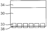
As shown in fig. 15E, after exposing the bottom of the resist 36, the Ag layer 35 is etched by ion milling (ion milling). After the Ag layer 35 is etched, the resist 36 remaining thereon is removed, thereby forming a nano-network metal 38 (metal thin film) having openings (through holes) in the Ag layer 35.
As shown in fig. 16A, a resist 39 is coated on the nano mesh metal 38 (metal thin film) and the p-type silicon single crystal substrate 30. The portion not doped with S, i.e., the long wavelength absorption layer 33, is exposed and developed using a photolithography method, thereby forming a resist pattern.
As shown in fig. 16B, the nano net-shaped metal 38 (metal thin film) is etched by ion milling using the resist pattern as a mask, thereby removing the nano net-shaped metal 38 (metal thin film). Then, the resist left after etching is removed. As a result, any portion of the nano mesh electrode 38 except for the portion just above the long wavelength absorption layer 33 is removed.
Further, as shown in fig. 16C, the rear electrode 40 is formed on a portion where the nano mesh metal 38 (metal thin film) has been removed by the lift-off process.
Finally, as shown in fig. 16D, a comb-shaped electrode 41 (first metal layer) is formed on the n + layer 34, thereby completing the photoelectric conversion element.
As described above, the photoelectric conversion element based on the silicon single crystal substrate has been described. In addition to the above-based photoelectric conversion element, another photoelectric conversion element based on a polycrystalline substrate, an amorphous silicon substrate, or a compound semiconductor substrate, which has the long-wavelength absorption layer 33 and a nano-network formed on the long-wavelength absorption layer 33, may be formed using a method similar to that described aboveMetal 38 (metal film). Further, examples of the material of the compound semiconductor substrate include GaAs, CdTe, and CIS (made of CuInSe)2Manufactured chalcopyrite compound semiconductor).
Examples of the invention
The photoelectric conversion element according to the embodiment will be described in more detail by way of example. The photoelectric conversion elements were formed to have a size of 9 square centimeters to evaluate their characteristics. Further, in the following examples, the manufacturing methods of the nano mesh metal and the dot metal are described for nano imprinting, but other methods (e.g., self-organization) can also be used to manufacture the nano mesh metal and the dot metal.
The profiles of examples 1-17 are listed in table 1.
[ Table 1]
Here, example 14 shows the highest photoelectric conversion efficiency, i.e., 14%, providing the best results in examples 1 to 17.
Example 1 (monocrystalline silicon, S, Ag, nano-mesh electrode)
A method of manufacturing a photoelectric conversion element according to example 1 will be described with reference to fig. 14A to 16D. Fig. 14A to 16D are sectional views showing manufacturing steps of the photoelectric conversion element according to the embodiment.
As shown in FIG. 14A, a p-type silicon single crystal substrate 30 was prepared to have a thickness of 500 μm and a thickness of 1X 10¹⁶A substrate with a doping concentration of cubic centimeters. A silicon dioxide film 31 having a thickness of 150 nm is formed on the p-type silicon single crystal substrate 30 by thermal oxidation.
As shown in fig. 14B, after a resist (THMR IP3250, TOKYO OHKA KOGYO co., Ltd.) solution was coated on the silicon oxide film 31 by spin coating at 2000rpm for 30 seconds, the coated resist was placed on a hot plate to be heatedHeat at 110 ℃ for 90 seconds to evaporate the solvent. The film thickness of the resist was 1 μm. Then, the resist was patterned into a grating shape having a width of 100 micrometers and a spacing of 1 mm by a photolithography method using a mask of a grating shape having a width of 100 micrometers and a spacing of 1 mm. The silicon dioxide film 31 was etched for 10 minutes under the conditions of 30sccm CF4, 10mTorr pressure, and 100WRF energy using the resist as a mask. At CF4After the RIE, the resist left after etching is removed by an organic solvent, thereby forming a grid-shaped silicon dioxide mask 32 having a width of 100 μm and a spacing of 1 mm.
Further, as shown in FIG. 14C, using the silicon dioxide mask 32 as a mask, the energy and 1X 10 are implanted at 20keV15Centimeter-2Implanting S ions under the condition of dosage.
As shown in fig. 14D, after removing the silicon dioxide mask 32 by hydrofluoric acid, activation annealing was performed at 1000 ℃ for 30 minutes to form the long wavelength absorption layer 33. In the long wavelength absorption layer 33, 1 × 10 is obtained within 100 nm from the silicon surface20Centimeter-3The concentration of (c).
As shown in FIG. 14E, the energy and 5X 10 are implanted at 20keV15Centimeter-2Under the condition of dosage, P ions are implanted into the opposite side faces of the S-doped silicon wafer. After ion implantation, an activation anneal is performed at 800 deg.C for 30 minutes to provide n + layer 34 with a 1 × 10 depth within 200 nanometers of the silicon surface20Centimeter-3The concentration of (c).
As shown in fig. 14F, an Ag layer 35 having a thickness of 30 nm was formed on the side surface which had been doped with S by an evaporation method.
Further, as shown in fig. 15A, the resist (THMRIP3250, TOKYO OHKA KOGYO co., Ltd.) was diluted 1: 2 by Ethyl Lactate (EL) to provide a resist solution. The solution was coated on the Ag layer 35 formed on the rear surface of the p-type silicon single crystal substrate 30 by spin coating. The coated resist was heated on a hot plate at 110 ℃ for 90 seconds to evaporate the solvent.
As shown in fig. 15B, with heating the p-type silicon single crystal substrate 30 having the resist 36 thereon, imprint is performed so that the quartz stamper 37 is pressed to the resist 36 under a pressure of 10 MPa. The quartz stamper 37 is provided with a convex shape having a size, a pitch, and a height of 100 nm, 200 nm, and 150 nm, respectively. When the quartz stamper 37 is pressed, its surface having a convex shape contacts the resist 36.
As shown in fig. 15C, after the imprinting, the p-type silicon single crystal substrate 30 is cooled and then the quartz stamper 37 is released. As a result, a concave shape having a size of 100 nm, a pitch of 200 nm, and a depth of 100 nm is formed on the resist 36.
As shown in fig. 15D, the resist 36 having a concave shape was etched by Reactive Ion Etching (RIE) of CF4 for 30 seconds under conditions of 30sccm CF4, 10mTorr pressure, and 100W RF energy, thereby exposing the bottom of the resist 36 to expose the Ag layer 35.
As shown in fig. 15E, the Ag layer 35 was etched by ion milling for 80 seconds under the conditions of an acceleration voltage of 500V and an ion current of 40mA to form a nano mesh electrode 38 having an opening (through hole). The Ag layer 35 was patterned by ion milling with an opening size of 100 nm and an opening pitch of 200 nm. Here, the residue of the resist 36 is removed by an organic solvent.
As shown in fig. 16A, after a solution of a resist (THMR IP3250, TOKYO OHKA KOGYO co., Ltd.) was coated on the nano mesh electrode 38 and the p-type silicon layer 30 by spin coating at 2000rpm for 30 seconds, the coated resist was heated at 110 ℃ for 90 seconds to evaporate the solvent. The film thickness of the resist 39 is 1 μm. The resist 39 is patterned into a grating shape by a photolithography method using a mask having a grating shape with a width of 100 μm and a spacing of 1 mm. The grid shape had a width of 100 microns and a spacing of 1 mm. This patterning exposes the non-S-doped portions instead of the long wavelength absorption layer 33.
Further, as shown in fig. 16B, the nano net-shaped metal electrode 38 was etched by ion milling for 80 seconds under the conditions of an acceleration voltage of 500V and an ion current of 40mA using the resist pattern as a mask to remove the nano net-shaped metal 38 (metal thin film). Then, the residue of the resist 39 is removed. As a result, the nano mesh electrode 38 except on the long wavelength absorption layer 33 is removed.
As shown in fig. 16C, a rear electrode 40 is formed on the portion where the nano mesh metal 38 (metal thin film) has been removed by the lift-off method.
Finally, as shown in fig. 16D, a comb-shaped electrode 41 (first metal layer) is formed on the n + layer 34 by a screen printing technique using Ag paste of thermosetting resin including an epoxy group, thereby realizing a photoelectric conversion element having the long wavelength absorption layer 33 and the nano mesh electrode 38.
(characteristics of solar cell)
The photoelectric conversion element manufactured as described above was irradiated with pseudo sunlight of AM1.5 and evaluated for photoelectric conversion efficiency at room temperature. As a result, the photoelectric conversion efficiency of the silicon single crystal photoelectric conversion element having the S-doped long wavelength absorption layer 33 and the nano mesh electrode 38 showed an excellent value of 12%.
On the other hand, the silicon single crystal photoelectric conversion element of the background art exhibits a photoelectric conversion efficiency of 10.0%. The silicon single crystal photoelectric conversion element of the background art has neither the S-doped long wavelength absorption layer 33 nor the nano mesh electrode 38.
Further, when evaluating the spectral sensitivity characteristics of the background-art silicon single-crystal photoelectric conversion element, light is absorbed in a range up to about 1100 nm. However, the silicon single crystal photoelectric conversion element of the embodiment of example 1 having the S-doped long wavelength absorption layer 33 and the nano mesh electrode 38 also has a light absorption spectrum in the range of 1100 nm to 1500 nm although the absorption intensity thereof is not so high.
The results indicate that the S-doped long wavelength absorption layer 33 and the nano mesh electrode 38 achieve an increase in photoelectric conversion efficiency in the long wavelength region of light due to light absorption in the long wavelength region of light. Example 2 (monocrystalline silicon, S, Au, nano-mesh electrode)
A method of manufacturing a photoelectric conversion element according to example 2 will be described with reference to fig. 17A to 19D. Fig. 17A to 19D are sectional views showing manufacturing steps of a photoelectric conversion element according to example 2.
As shown in FIG. 17A, a film having a thickness of 500 μm and a thickness of 1X 10 was prepared16Centimeter-3The p-type silicon single crystal substrate 30 of doping concentration of (a) is used as a substrate. The surface of the p-type silicon single crystal substrate 30 is thermally oxidized to form a silicon dioxide film 31 having a thickness of 150 nm.
As shown in fig. 17B, after a resist (THMR IP3250, TOKYO OHKA KOGYO co., Ltd.) solution was coated on the silicon oxide film 31 by spin coating at 2000rpm for 30 seconds, the coated resist was heated on a hot plate at 110 ℃ for 90 seconds to evaporate the solvent. The film thickness of the resist was 1 μm. The resist was patterned into a grating shape by a photolithography method using a grating-shaped mask having a width of 100 μm and a spacing of 1 mm. The grid shape had a width of 100 microns and a spacing of 1 mm. The silicon dioxide film 31 was etched for 10 minutes under the conditions of 30-sccm CF4, 10mTorr pressure, and 100W RF energy using the resist as a mask. Subsequently, the residue of the resist was removed by an organic solvent to form a grid-shaped silicon dioxide mask 32 having a width of 100 μm and a spacing of 1 mm.
Furthermore, as shown in FIG. 17C, the implantation energy sum at 20keV was 1X 10¹⁵Centimeter-2Using the silicon dioxide mask 32, S ions are implanted.
As shown in fig. 17D, after removing the silicon dioxide mask 32 with hydrofluoric acid, activation annealing is performed at 1000 ℃ for 30 minutes to form the long wavelength absorption layer 33. In the long wavelength absorption layer 33, 1 × 10 is obtained within a depth of 100 nm from the silicon surface20Centimeter-3The concentration of (c).
As shown in FIG. 17E, the energy and 5X 10 are implanted at 20keV15Centimeter-2Under the condition of dosage, P ions are implanted at the side opposite to the side where S is doped. After ion implantation, activation annealing is performed at 800 deg.C30 minutes, to provide n + layer 34 with a 1 x 10 depth of 200 nanometers from the silicon surface20Centimeter-3The concentration of (c).
As shown in fig. 17F, an Au layer having a thickness of 30 nm is formed on the side surface which has been doped with S by an evaporation method, thereby forming an Au layer 50.
Further, as shown in fig. 18A, after a resist solution was coated on the Au layer 50 formed on the p-type silicon single crystal substrate 30 by spin coating at 2000rpm for 30 seconds, the coated resist was heated at 110 ℃ for 90 seconds on a heating plate to evaporate the solvent. The resist solution was obtained by diluting the resist 36(THMR IP3250, TOKYO OHKA KOGYO co., Ltd.) with Ethyl Lactate (EL) at 1: 2. The film thickness of the resist 36 was 150 nm.
As shown in fig. 18B, the imprint is performed as follows. In the case of heating the p-type silicon single crystal substrate 30 at 120 ℃, the quartz stamper 37 is pressed to the resist 36 at a pressure of 10MPa so that the surface of the quartz stamper 37 having a convex shape contacts the resist 36. The quartz stamper 37 is provided with a convex shape having a size, a pitch, and a height of 300 nm, 150 nm, and 150 nm, respectively (the shape forms an area of 9 square centimeters).
Further, as shown in fig. 18C, after the imprinting, the p-type silicon single crystal substrate 30 was cooled to room temperature, and then the quartz stamper 37 was released. The imprinting forms recessed shapes on resist 36 having a pitch of 300 nanometers, a dimension of 150 nanometers, and a depth of 100 nanometers.
As shown in fig. 18D, the resist pattern on which the recessed pattern has been formed is etched for 30 seconds under the condition of 30sccm CF4, 10mTorr pressure and 100W RF energy. After the CF4RIE, the bottom of the resist 36 is exposed to expose the Au layer 50.
As shown in fig. 18E, the Au layer 50 was etched by ion milling for 90 seconds under the conditions of an acceleration voltage of 500V and an ion current of 40mA to form the nano mesh electrode 38 having an opening (through hole). Ion milling patterns the Au layer 50. The pattern has openings (vias) with a size of 150 nm and a pitch of 300 nm. Further, the residue of the resist 36 is removed by an organic solvent.
As shown in fig. 19A, after a solution of a resist (THMR IP3250, TOKYO OHKA KOGYO co., Ltd.) was coated on the nano mesh electrode 38 and the p-type silicon layer 30 by spin coating at 2000rpm for 30 seconds, the coated resist was heated at 110 ℃ for 90 seconds to evaporate the solvent. The film thickness of the resist 39 is 1 μm. The resist 39 is patterned into a grating shape by a photolithography method using a mask having a grating shape with a width of 100 μm and a spacing of 1 mm. The grid shape had a width of 100 microns and a spacing of 1 mm. The patterning exposes portions other than the long wavelength absorption layer 33 not doped with S.
Further, as shown in fig. 19B, the nano net-shaped metal electrode 38 was etched by ion milling for 90 seconds under the conditions of an acceleration voltage of 500V and an ion current of 40mA using the resist pattern as a mask, thereby removing the nano net-shaped electrode 38. Then, the residue of the resist 39 is removed. As a result, the nano mesh electrode 38 except on the long wavelength absorption layer 33 is removed.
As shown in fig. 19C, the rear electrode 40 is formed on the portion where the nano mesh electrode 38 is not present by the lift-off method.
Finally, as shown in fig. 19D, a comb-shaped electrode 41 (first metal layer) was formed on the n + layer 34 by a screen printing method using Ag paste of thermosetting resin including an epoxy group, thereby realizing a silicon photoelectric conversion element having the long wavelength absorption layer 33 and the nano mesh electrode 38.
(characteristics of solar cell)
The photoelectric conversion element manufactured as described above was irradiated with pseudo sunlight of AM1.5 and evaluated for photoelectric conversion efficiency at room temperature. As a result, the photoelectric conversion efficiency of the silicon single crystal photoelectric conversion element having the S-doped long wavelength absorption layer 33 and the nano mesh electrode 38 exhibited an excellent value of 11.8%.
On the other hand, the silicon single crystal photoelectric conversion element of the background art exhibits a photoelectric conversion efficiency of 10.0% without the S-doped long wavelength absorption layer 33 or the nano mesh electrode 38.
Further, when evaluating the spectral sensitivity characteristics of the background-art silicon single-crystal photoelectric conversion element, light is absorbed in a range up to about 1100 nm. However, the silicon single crystal photoelectric conversion element of the embodiment of example 2 having the S-doped long wavelength absorption layer 33 and the nano mesh electrode 38 also has a light absorption spectrum in the range of 1100 nm to 1500 nm although the absorption intensity thereof is not so high.
The results indicate that the S-doped long wavelength absorption layer 33 and the nano mesh electrode 38 achieve an increase in photoelectric conversion efficiency in the long wavelength region of light due to light absorption in the long wavelength region of light. Example 3 (Single crystal silicon, S-O, Cu, nanometer mesh electrode)
A method of manufacturing a photoelectric conversion element according to example 3 will be described with reference to fig. 20A to 22D. Fig. 20A to 22D are sectional views showing manufacturing steps of a photoelectric conversion element according to example 3.
As shown in FIG. 20A, a film having a thickness of 500 μm and a thickness of 1X 10 was prepared16Centimeter-3The p-type silicon single crystal substrate 30 of doping concentration of (a) is used as a substrate. The surface of the p-type silicon single crystal substrate 30 is thermally oxidized to form a silicon dioxide film 31 having a thickness of 150 nm.
As shown in fig. 20B, after a resist (THMR IP3250, TOKYO OHKA KOGYO co., Ltd.) solution was coated on the silicon dioxide film 31 by spin coating at 2000rpm for 30 seconds, the coated resist was heated on a hot plate at 110 ℃ for 90 seconds to evaporate the solvent. The film thickness of the resist was 1 μm. The resist was patterned into a grating shape by a photolithography method using a grating-shaped mask having a width of 100 μm and a spacing of 1 mm. The grid shape had a width of 100 microns and a spacing of 1 mm. The silicon dioxide film 31 was etched for 10 minutes under conditions of 30-sccm CF4, 10mTorr pressure, and 100WRF energy using the resist as a mask. Subsequently, the residue of the resist was removed by an organic solvent to form a silicon dioxide mask 32 having a grid shape with a width of 100 μm and a spacing of 1 mm.
Furthermore, as shown in FIG. 20C, the implantation energy sum at 20keV was 1X 10¹⁵Centimeter-2Using the silicon dioxide mask 32 as a mask, S and O ions are implanted simultaneously.
As shown in fig. 20D, after removing the silicon dioxide mask 32 with hydrofluoric acid, activation annealing is performed at 1000 ℃ for 30 minutes to form the long wavelength absorption layer 33. In the long wavelength absorption layer 33, 1 × 10 is obtained within a depth of 100 nm from the silicon surface20Centimeter-3The concentration of (c).
As shown in FIG. 20E, the energy and the energy of the implant are 5X 10 at 20keV15Centimeter-2Under the condition of dosage, P ions are implanted at the side opposite to the side where S and O are doped. After ion implantation, an activation anneal is performed at 800 deg.C for 30 minutes to provide n + layer 34 with a 1X 10 depth within 200 nanometers of the silicon surface20Centimeter-3The concentration of (c).
As shown in fig. 20F, a Cu layer having a thickness of 30 nm is formed on the side surface which has been doped with S by an evaporation method, thereby forming a Cu layer 51.
Further, as shown in fig. 21A, after a resist solution was coated on the Cu layer 51 formed on the p-type silicon single crystal substrate 30 by spin coating at 2000rpm for 30 seconds, the coated resist was heated at 110 ℃ for 90 seconds on a heating plate to evaporate the solvent. The resist solution was obtained by diluting the resist 36(THMR IP3250, TOKYO OHKA KOGYO co., Ltd.) with Ethyl Lactate (EL) at 1: 2. The film thickness of the resist 36 was 150 nm.
As shown in fig. 21B, the imprint is performed as follows. In the case of heating the p-type silicon single crystal substrate 30 at 120 ℃, the quartz stamper 37 is pressed to the resist 36 at a pressure of 10MPa so that the surface of the quartz stamper 37 having a convex shape contacts the resist 36. The quartz stamper 37 is provided with a convex shape having a size, a pitch, and a height of 400 nm, 200 nm, and 150 nm, respectively (the shape forms an area of 9 square centimeters).
Further, as shown in fig. 21C, after the imprinting, the p-type silicon single crystal substrate 30 was cooled to room temperature, and then the quartz stamper 37 was released. The imprinting forms recessed shapes on resist 36 having a 400 nanometer pitch, a 150 nanometer dimension, and a depth of 100 nanometers.
As shown in fig. 21D, the resist pattern on which the recessed pattern has been formed is etched for 30 seconds under 30sccm CF4, a pressure of 10mTorr, and 100W RF energy. After the CF4RIE, the bottom of the resist 36 is exposed to expose the Cu layer 51.
As shown in fig. 21E, the Cu layer 51 was etched by ion milling for 90 seconds under the conditions of an acceleration voltage of 500V and an ion current of 40mA to form the nano mesh electrode 38 having an opening (through hole). Ion milling forms a pattern on the Cu layer 51. The pattern has openings (vias) with a size of 150 nm and a pitch of 300 nm. Further, the residue of the resist 36 is removed by an organic solvent.
As shown in fig. 22A, after a solution of a resist 39(THMRIP3250, TOKYO OHKA KOGYO co., Ltd.) was applied onto the nano mesh electrode 38 and the p-type silicon layer 30 by spin coating at 2000rpm for 30 seconds, the applied resist was heated at 110 ℃ for 90 seconds to evaporate the solvent. The film thickness of the resist 39 is 1 μm. The resist 39 is patterned into a grating shape by a photolithography method using a mask having a grating shape with a width of 100 μm and a spacing of 1 mm. The grid shape had a width of 100 microns and a spacing of 1 mm. The patterning exposes portions that are not doped with S.
Further, as shown in fig. 22B, the nano mesh metal electrode 38 was etched by ion milling for 90 seconds under the conditions of an acceleration voltage of 500V and an ion current of 40mA using the resist pattern as a mask, thereby removing the nano mesh electrode 38. Then, the residue of the resist 39 is removed. As a result, the nano mesh electrode 38 except on the long wavelength absorption layer 33 is removed.
As shown in fig. 22C, the rear electrode 40 is formed on a portion where the nano mesh electrode 38 is not present by the lift-off method.
Finally, as shown in fig. 22D, a comb-shaped electrode 41 (first metal layer) was formed on the n + layer 34 by a screen printing method using Ag paste of thermosetting resin including an epoxy group, thereby realizing a silicon photoelectric conversion element having the long wavelength absorption layer 33 and the nano mesh electrode 38.
(characteristics of solar cell)
The photoelectric conversion element manufactured as described above was irradiated with pseudo sunlight of AM1.5 and evaluated for photoelectric conversion efficiency at room temperature. As a result, the photoelectric conversion efficiency of the silicon single crystal photoelectric conversion element having the S and O doped long wavelength absorption layer 33 and the nano mesh electrode 38 showed an excellent value of 12.5%.
On the other hand, the silicon single crystal photoelectric conversion element of the background art exhibits a photoelectric conversion efficiency of 10.0% without the S and O doped long wavelength absorption layer 33 or the nano mesh electrode 38.
Further, when evaluating the spectral sensitivity characteristics of the background-art silicon single-crystal photoelectric conversion element, light is absorbed in a range up to about 1100 nm. However, the silicon single crystal photoelectric conversion element of the embodiment of example 3 having the S-doped long wavelength absorption layer 33 and the nano mesh electrode 38 also has a light absorption spectrum in the range of 1100 nm to 1500 nm although the absorption intensity thereof is not so high. S and O can form an S-O absorption pair, thereby improving the absorption and conversion efficiency compared to single S doping.
The results indicate that the S and O doped long wavelength absorption layer 33 and the nano mesh electrode 38 achieve an increase in photoelectric conversion efficiency in the long wavelength region of light due to light absorption in the long wavelength region of light. Example 4 (Single crystal silicon, Se, Ag, nano-mesh electrode)
A method of manufacturing a photoelectric conversion element according to example 4 will be described with reference to fig. 23A to 25D. Fig. 23A to 25D are sectional views showing manufacturing steps of a photoelectric conversion element according to example 4.
As shown in FIG. 23A, a film having a thickness of 500 μm and a thickness of 1X 10 was prepared16Centimeter-3Doping concentration ofThe p-type silicon single crystal substrate 30 as a substrate. The surface of the p-type silicon single crystal substrate 30 is thermally oxidized to form a silicon dioxide film 31 having a thickness of 150 nm.
As shown in fig. 23B, after a solution of a resist (THMR IP3250, TOKYO OHKA KOGYO co., Ltd.) was coated on the silicon oxide film 31 by spin coating at 2000rpm for 30 seconds, the coated resist was heated at 110 ℃ for 90 seconds on a hot plate to evaporate the solvent. The film thickness of the resist was 1 μm. The resist was patterned into a grating shape by a photolithography method using a grating-shaped mask having a width of 100 μm and a spacing of 1 mm. The grid shape had a width of 100 microns and a spacing of 1 mm. The silicon dioxide film 31 was etched for 10 minutes under the conditions of 30-sccm CF4, 10mTorr pressure, and 100W RF energy using the resist as a mask. Subsequently, the residue of the resist was removed by an organic solvent to form a grid-shaped silicon dioxide mask 32 having a width of 100 μm and a spacing of 1 mm.
Further, as shown in FIG. 23C, using the silicon dioxide mask 32 as a mask, the implantation energy and 1X 10 are applied at 20keV15Centimeter-2Under the dosage of (4), Se ions are implanted using the silicon dioxide mask 32 as a mask.
As shown in fig. 23D, after removing the silicon dioxide mask 32 by hydrofluoric acid, activation annealing was performed at 1000 ℃ for 30 minutes to form the long wavelength absorption layer 33. In the long wavelength absorption layer 33, 1 × 10 is obtained within a depth of 100 nm from the silicon surface20Centimeter-3The concentration of (c).
As shown in FIG. 23E, the implantation energy sum is 5X 10 at 20keV15Centimeter-2P is ion implanted under dose conditions on the opposite side of the already doped Se. After ion implantation, an activation anneal is performed at 800 deg.C for 30 minutes to provide n + layer 34 with a 1 × 10 depth within 200 nanometers of the silicon surface20Centimeter-3The concentration of (c).
As shown in fig. 23F, an Ag layer having a thickness of 30 nm was formed on the side that had been doped with Se by an evaporation method, thereby forming an Ag layer 35.
Further, as shown in fig. 24A, after a resist solution was coated on the Ag layer 35 formed on the p-type silicon single crystal substrate 30 by spin coating at 2000rpm for 30 seconds, the coated resist was heated at 110 ℃ for 90 seconds on a heating plate to evaporate the solvent. The resist solution was obtained by diluting the resist 36(THMR IP3250, TOKYO OHKA KOGYO co., Ltd.) with Ethyl Lactate (EL) at 1: 2. The film thickness of the resist 36 was 150 nm.
As shown in fig. 24B, the imprint is performed as follows. In the case of heating the p-type silicon single crystal substrate 30 at 120 ℃, the quartz stamper 37 is pressed to the resist 36 at a pressure of 10MPa so that the surface of the quartz stamper 37 having a convex shape contacts the resist 36. The quartz stamper 37 is provided with a convex shape having a size, a pitch, and a height of 200 nm, 100 nm, and 150 nm, respectively (the shape forms an area of 9 square centimeters).
Further, as shown in fig. 24C, after the imprint, the p-type silicon single crystal substrate 30 was cooled to room temperature, and then the quartz stamper 37 was released. The imprinting forms recessed shapes on resist 36 having a 400 nanometer pitch, a 150 nanometer dimension, and a depth of 100 nanometers.
As shown in fig. 24D, the resist pattern on which the recessed pattern has been formed is etched for 30 seconds under 30sccm CF4, a pressure of 10mTorr, and 100W RF energy. At CF4After RIE, the bottom of the resist 36 is exposed to expose the Ag layer 35.
As shown in fig. 24E, the Ag layer 35 was etched by ion milling for 90 seconds under the conditions of an acceleration voltage of 500V and an ion current of 40mA to form a nano mesh electrode 38 having an opening (through hole). Ion milling forms a pattern on the Ag layer 35. The pattern has openings (vias) with a size of 150 nm and a pitch of 300 nm. Further, the residue of the resist 36 is removed by an organic solvent.
As shown in fig. 25A, after a solution of a resist 39(THMRIP3250, TOKYO OHKA KOGYO co., Ltd.) was coated on the nano mesh electrode 38 and the p-type silicon layer 30 by spin coating at 2000rpm for 30 seconds, the coated resist was heated at 110 ℃ for 90 seconds to evaporate the solvent. The film thickness of the resist 39 is 1 μm. The resist 39 is patterned into a grating shape by a photolithography method using a mask having a grating shape with a width of 100 μm and a spacing of 1 mm. The grating shape had a width of 100 micrometers and a spacing of 1 mm, thereby exposing a portion not doped with Se.
Further, as shown in fig. 25B, the nano net-shaped metal electrode 38 was etched by ion milling for 90 seconds under the conditions of an acceleration voltage of 500V and an ion current of 40mA using the resist pattern as a mask, thereby removing the nano net-shaped electrode 38. Then, the residue of the resist 39 is removed. As a result, the nano mesh electrode 38 except on the long wavelength absorption layer 33 is removed.
As shown in fig. 25C, the rear electrode 40 is formed on the portion where the nano mesh electrode 38 is not present by the lift-off method.
Finally, as shown in fig. 25D, a comb-shaped electrode 41 (first metal layer) was formed on the n + layer 34 by a screen printing method using Ag paste of thermosetting resin including an epoxy group, thereby realizing a silicon photoelectric conversion element having the long wavelength absorption layer 33 and the nano mesh electrode 38.
(characteristics of solar cell)
The photoelectric conversion element manufactured as described above was irradiated with pseudo sunlight of AM1.5 and evaluated for photoelectric conversion efficiency at room temperature. As a result, the photoelectric conversion efficiency of the silicon single crystal photoelectric conversion element of example 4 having the Se-doped long wavelength absorption layer 33 and the nano mesh electrode 38 exhibited an excellent value of 13%.
On the other hand, the silicon single crystal photoelectric conversion element of the background art exhibits a photoelectric conversion efficiency of 10.0% without the Se-doped long wavelength absorption layer 33 or the nano mesh electrode 38.
Further, when evaluating the spectral sensitivity characteristics of the background-art silicon single-crystal photoelectric conversion element, light is absorbed in a range up to about 1100 nm. However, the silicon single crystal photoelectric conversion element having the Se-doped long-wavelength absorption layer 33 and the nano mesh electrode 38 also has a light absorption spectrum in the range of 1100 nm to 1500 nm, although the absorption intensity thereof is not so high.
The results indicate that the Se-doped long wavelength absorption layer 33 and the nano mesh electrode 38 achieve an increase in photoelectric conversion efficiency in the long wavelength region of light due to light absorption in the long wavelength region of light. Example 5 (Single crystal silicon, In, Au, nano mesh electrode)
A method of manufacturing a photoelectric conversion element according to example 5 will be described with reference to fig. 26A to 28D. Fig. 26A to 28D are sectional views showing manufacturing steps of a photoelectric conversion element according to example 5.
As shown in FIG. 26A, a film having a thickness of 500 μm and a thickness of 1X 10 was prepared16Centimeter-3The p-type silicon single crystal substrate 30 of doping concentration of (a) is used as a substrate. The surface of the p-type silicon single crystal substrate 30 is thermally oxidized to form a silicon dioxide film 31 having a thickness of 150 nm.
As shown in fig. 26B, after a solution of a resist (THMR IP3250, TOKYO OHKA KOGYO co., Ltd.) was coated on the silicon oxide film 31 by spin coating at 2000rpm for 30 seconds, the coated resist was heated at 110 ℃ for 90 seconds on a hot plate to evaporate the solvent. The film thickness of the resist was 1 μm. The resist was patterned into a grating shape by a photolithography method using a grating-shaped mask having a width of 100 μm and a spacing of 1 mm. The grid shape had a width of 100 microns and a spacing of 1 mm. Using the resist as a mask, at 30-sccm CF4The silicon dioxide film 31 was etched for 10 minutes under the conditions of a pressure of 10mTorr and RF energy of 100W. Subsequently, the residue of the resist was removed with an organic solvent to form a grid-shaped silicon dioxide mask 32 having a width of 100 μm and a spacing of 1 mm.
Further, as shown in FIG. 26C, using the silicon dioxide mask 32 as a mask, the implantation energy and 1X 10 are applied at 20keV15Centimeter-2In ion implantation using the silicon dioxide mask 32 as a mask.
As shown in fig. 26D, after removing the silicon dioxide mask 32 with hydrofluoric acid, activation annealing is performed at 1000 ℃ for 30 minutes to form the long wavelength absorption layer 33. In the long wavelength absorption layer 33, 1 × 10 is obtained within a depth of 100 nm from the silicon surface20Centimeter-3The concentration of (c).
As shown in FIG. 26E, the energy and 5X 10 are implanted at 20keV15Centimeter-2Under the condition of dosage, P ions are implanted at the side opposite to the side where the In is doped. After ion implantation, an activation anneal is performed at 800 deg.C for 30 minutes to provide n + layer 34 with a 1 × 10 depth within 200 nanometers of the silicon surface20Centimeter-3The concentration of (c).
As shown In fig. 26F, an Au layer having a thickness of 30 nm was formed on the side surface which had been doped with In by an evaporation method, thereby forming an Au layer 50.
Further, as shown in fig. 27A, after a resist solution was coated on the Au layer 50 formed on the p-type silicon single crystal substrate 30 by spin coating at 2000rpm for 30 seconds, the coated resist was heated at 110 ℃ for 90 seconds on a heating plate to evaporate the solvent. The resist solution was obtained by diluting the resist 36(THMR IP3250, TOKYO OHKA KOGYO co., Ltd.) with Ethyl Lactate (EL) at 1: 2. The film thickness of the resist 36 was 150 nm.
As shown in fig. 27B, the imprint is performed as follows. In the case of heating the p-type silicon single crystal substrate 30 at 120 ℃, the quartz stamper 37 is pressed to the resist 36 at a pressure of 10MPa so that the surface of the quartz stamper 37 having a convex shape contacts the resist 36. The quartz stamper 37 is provided with a convex shape having a size, a pitch, and a height of 300 nm, 150 nm, and 150 nm, respectively (the shape forms an area of 9 square centimeters).
Further, as shown in fig. 27C, after the imprinting, the p-type silicon single crystal substrate 30 was cooled to room temperature, and then the quartz stamper 37 was released. The imprinting forms recessed shapes on resist 36 having a pitch of 300 nanometers, a size of 150 nanometers, and a depth of 100 nanometers.
As shown in fig. 27D, the resist pattern on which the recessed pattern has been formed is etched under 30sccm CF4, a pressure of 10mTorr, and 100W RF energy for 30 seconds. After the CF4RIE, the bottom of resist 36 is exposed to expose Au layer 50.
As shown in fig. 27E, the Au layer 50 was etched by ion milling for 90 seconds under the conditions of an acceleration voltage of 500V and an ion current of 40mA to form the nano mesh electrode 38 having an opening (through hole). The Au layer 50 is patterned by ion milling. The pattern has openings (vias) with a size of 150 nm and a pitch of 300 nm. Further, the residue of the resist 36 is removed by an organic solvent.
As shown in fig. 28A, after a solution of a resist 39(THMRIP3250, TOKYO OHKA KOGYO co., Ltd.) was coated on the nano mesh electrode 38 and the p-type silicon layer 30 by spin coating at 2000rpm for 30 seconds, the coated resist was heated at 110 ℃ for 90 seconds to evaporate the solvent. The film thickness of the resist 39 is 1 μm. The resist 39 is patterned into a grating shape by a photolithography method using a mask having a grating shape with a width of 100 μm and a spacing of 1 mm. The grid shape had a width of 100 microns and a spacing of 1 mm. The patterning exposes portions that are not doped with In.
Further, as shown in fig. 28B, the nano mesh metal electrode 38 was etched by ion milling for 90 seconds under the conditions of an acceleration voltage of 500V and an ion current of 40mA using the resist pattern as a mask, thereby removing the nano mesh electrode 38. Then, the residue of the resist 39 is removed. As a result, the nano mesh electrode 38 except on the long wavelength absorption layer 33 is removed.
As shown in fig. 28C, the rear electrode 40 is formed on the portion where the nano mesh electrode 38 is not present by the lift-off method.
Finally, as shown in fig. 28D, a comb-shaped electrode 41 (first metal layer) was formed on the n + layer 34 by a screen printing method using Ag paste of thermosetting resin including an epoxy group, thereby realizing a silicon photoelectric conversion element having the long wavelength absorption layer 33 and the nano mesh electrode 38.
(characteristics of solar cell)
The photoelectric conversion element manufactured as described above was irradiated with pseudo sunlight of AM1.5 and evaluated for photoelectric conversion efficiency at room temperature. As a result, the photoelectric conversion efficiency of the silicon single crystal photoelectric conversion element of the example 5 embodiment having the Se-doped long wavelength absorption layer 33 and the nano mesh electrode 38 exhibited an excellent value of 11.5%.
On the other hand, the silicon single crystal photoelectric conversion element of the background art exhibits a photoelectric conversion efficiency of 10.0% without the In-doped long wavelength absorption layer 33 or the nano mesh electrode 38.
Further, when evaluating the spectral sensitivity characteristics of the background-art silicon single-crystal photoelectric conversion element, light is absorbed in a range up to about 1100 nm. However, the silicon single crystal photoelectric conversion element having the In-doped long wavelength absorption layer 33 and the nano mesh electrode 38 also has a light absorption spectrum In the range of 1100 nm to 1500 nm, although the absorption intensity thereof is not so high.
The results indicate that the In-doped long wavelength absorption layer 33 and the nano mesh electrode 38 achieve an increase In photoelectric conversion efficiency In the long wavelength region of light due to light absorption In the long wavelength region of light. Example 6 (Single crystal silicon, In, Au, nano mesh electrode)
A method of manufacturing a photoelectric conversion element according to example 6 will be described with reference to fig. 29A to 31D. Fig. 29A to 31D are sectional views showing manufacturing steps of a photoelectric conversion element according to example 6.
As shown in FIG. 29A, a film having a thickness of 500 μm and a thickness of 1X 10 was prepared16Centimeter-3The p-type silicon single crystal substrate 30 of doping concentration of (a) is used as a substrate. The surface of the p-type silicon single crystal substrate 30 is thermally oxidized to form a silicon dioxide film 31 having a thickness of 150 nm.
As shown in fig. 29B, after a solution of a resist (THMR IP3250, TOKYO OHKA KOGYO co., Ltd.) was coated on the silicon oxide film 31 by spin coating at 2000rpm for 30 seconds, the coated resist was heated at 110 ℃ for 90 seconds on a hot plate to evaporate the solvent. The film thickness of the resist was 1 μm. The resist was patterned into a grating shape by a photolithography method using a grating-shaped mask having a width of 100 μm and a spacing of 1 mm. The grid shape had a width of 100 microns and a spacing of 1 mm. The silicon dioxide film 31 was etched for 10 minutes under the conditions of 30-sccm CF4, 10mTorr pressure, and 100W RF energy using the resist as a mask. Subsequently, the residue of the resist was removed by an organic solvent to form a grid-shaped silicon dioxide mask 32 having a width of 100 μm and a spacing of 1 mm.
Furthermore, as shown in FIG. 29C, the implantation energy sum at 20keV was 1X 10¹⁵Centimeter-2Using the silicon dioxide mask 32 as a mask, Mg and Ga ions are implanted simultaneously.
As shown in fig. 29D, after the silicon dioxide mask 32 is removed by hydrofluoric acid, activation annealing is performed at 1000 ℃ for 30 minutes to form the long wavelength absorption layer 33. In the long wavelength absorption layer 33, 1 × 10 is obtained within a depth of 100 nm from the silicon surface20Centimeter-3The concentration of (c).
As shown in FIG. 29E, the energy and 5X 10 are implanted at 20keV15Centimeter-2Under the condition of dosage, P ions are implanted at the side opposite to the side which is doped with Mg and Ga. After ion implantation, an activation anneal is performed at 800 deg.C for 30 minutes to provide n + layer 34 with a 1 × 10 depth within 200 nanometers of the silicon surface20Centimeter-3The concentration of (c).
As shown in fig. 29F, a Cu layer having a thickness of 30 nm was formed on the side that had been doped with Mg and Ga by an evaporation method, thereby forming a Cu layer 51.
Further, as shown in fig. 30A, after a resist solution was coated on the Cu layer 51 formed on the p-type silicon single crystal substrate 30 by spin coating at 2000rpm for 30 seconds, the coated resist was heated at 110 ℃ for 90 seconds on a heating plate to evaporate the solvent. The resist solution was obtained by diluting the resist 36(THMR IP3250, TOKYO OHKA KOGYO co., Ltd.) with Ethyl Lactate (EL) at 1: 2. The film thickness of the resist 36 was 150 nm.
As shown in fig. 30B, the imprint is performed as follows. In the case of heating the p-type silicon single crystal substrate 30 at 120 ℃, the quartz stamper 37 is pressed to the resist 36 at a pressure of 10MPa so that the surface of the quartz stamper 37 having a convex shape contacts the resist 36. The quartz stamper 37 is provided with a convex shape having a size, a pitch, and a height of 300 nm, 150 nm, and 150 nm, respectively (the shape forms an area of 9 square centimeters).
Further, as shown in fig. 30C, after the imprinting, the p-type silicon single crystal substrate 30 was cooled to room temperature, and then the quartz stamper 37 was released. The imprinting forms recesses in resist 36 having a 400 nanometer pitch, 200 nanometer size, and a depth of 100 nanometers.
As shown in fig. 30D, the resist pattern on which the recessed pattern has been formed is etched under 30sccm CF4, a pressure of 10mTorr, and 100W RF energy for 30 seconds. After the CF4RIE, the bottom of the resist 36 is exposed to expose the Cu layer 51.
As shown in fig. 30E, the Cu layer 51 was etched by ion milling for 90 seconds under the conditions of an acceleration voltage of 500V and an ion current of 40mA to form the nano mesh electrode 38 having an opening (through hole). Ion milling forms a pattern on the Cu layer 51. The pattern has openings (vias) with a size of 200 nm and a pitch of 400 nm. Further, the residue of the resist 36 is removed by an organic solvent.
As shown in fig. 31A, after a solution of a resist 39(THMRIP3250, TOKYO OHKA KOGYO co., Ltd.) was coated on the nano mesh electrode 38 and the p-type silicon layer 30 by spin coating at 2000rpm for 30 seconds, the coated resist was heated at 110 ℃ for 90 seconds to evaporate the solvent. The film thickness of the resist 39 is 1 μm. The resist 39 is patterned into a grating shape by a photolithography method using a mask having a grating shape with a width of 100 μm and a spacing of 1 mm. The grid shape had a width of 100 microns and a spacing of 1 mm. The patterning exposes portions that are not doped with Mg and Ga.
Further, as shown in fig. 31B, the nano net-shaped metal electrode 38 was etched by ion milling for 90 seconds under the conditions of an acceleration voltage of 500V and an ion current of 40mA using the resist pattern as a mask, thereby removing the nano net-shaped electrode 38. Then, the residue of the resist 39 is removed. As a result, the nano mesh electrode 38 except on the long wavelength absorption layer 33 is removed.
As shown in fig. 31C, the rear electrode 40 is formed on the portion where the nano mesh electrode 38 is not present by the lift-off method.
Finally, as shown in fig. 31D, a comb-shaped electrode 41 (first metal layer) was formed on the n + layer 34 by a screen printing method using Ag paste of thermosetting resin including an epoxy group, thereby realizing a silicon photoelectric conversion element having the long wavelength absorption layer 33 and the nano mesh electrode 38.
(characteristics of solar cell)
The photoelectric conversion element manufactured as described above was irradiated with pseudo sunlight of AM1.5 and evaluated for photoelectric conversion efficiency at room temperature. As a result, the photoelectric conversion efficiency of the silicon single crystal photoelectric conversion element of the example 6 having the Mg and Ga doped long wavelength absorption layer 33 and the nano mesh electrode 38 exhibited an excellent value of 11.5%.
On the other hand, the silicon single crystal photoelectric conversion element of the background art exhibits a photoelectric conversion efficiency of 10.0% without the Mg and Ga doped long wavelength absorption layer 33 or the nano mesh electrode 38.
Further, when evaluating the spectral sensitivity characteristics of the background-art silicon single-crystal photoelectric conversion element, light is absorbed in a range up to about 1100 nm. However, the silicon single crystal photoelectric conversion element having the Mg and Ga doped long wavelength absorption layer 33 and the nano mesh electrode 38 also has a light absorption spectrum in the range of 1100 nm to 1400 nm although the absorption intensity thereof is not so high.
The results indicate that the Mg and Ga doped long wavelength absorption layer 33 and the nano mesh electrode 38 achieve an increase in photoelectric conversion efficiency in the long wavelength region of light due to light absorption in the long wavelength region of light.
Further, Mg has an energy level on one side of the conduction band, and Ga has an energy level on one side of the valence band. The absorption band of light is generated in a long wavelength region of light by absorption between two energy levels. As described above, the absorption band of light is rarely generated in the long wavelength region of light by one impurity level. Light absorption in the long wavelength region of such light is achieved using two or more impurity levels. Example 7 (thin single crystal silicon, S, Ag, nano-mesh electrode)
A method of manufacturing a photoelectric conversion element according to example 7 will be described with reference to fig. 14A to 16D. Fig. 14A to 16D are sectional views showing manufacturing steps of a photoelectric conversion element according to example 7.
As shown in FIG. 14A, a film having a thickness of 100 μm and a thickness of 1X 10 was prepared16Centimeter-3The p-type silicon single crystal substrate 30 of doping concentration of (a) is used as a substrate. The surface of the p-type silicon single crystal substrate 30 is thermally oxidized to form a silicon dioxide film 31 having a thickness of 150 nm.
As shown in fig. 14B, after a solution of a resist (THMR IP3250, TOKYO OHKA KOGYO co., Ltd.) was coated on the silicon oxide film 31 by spin coating at 2000rpm for 30 seconds, the coated resist was heated at 110 ℃ for 90 seconds on a hot plate to evaporate the solvent. The film thickness of the resist was 1 μm. The resist was patterned into a grating shape by a photolithography method using a grating-shaped mask having a width of 100 μm and a spacing of 1 mm. The grid shape had a width of 100 microns and a spacing of 1 mm. The silicon dioxide film 31 was etched for 10 minutes under the conditions of 30-sccm CF4, 10mTorr pressure, and 100W RF energy using the resist as a mask. Subsequently, the residue of the resist was removed by an organic solvent to form a grid-shaped silicon dioxide mask 32 having a width of 100 μm and a spacing of 1 mm.
Furthermore, as shown in FIG. 14C, the implantation energy sum at 20keV was 1X 10¹⁵Centimeter-2Using the silicon dioxide mask 32 as a mask, S ions are implanted under the dosage conditions of (a).
As shown in FIG. 14D, the silicon dioxide mask is removed by hydrofluoric acidAfter 32, activation annealing is performed at 1000 ℃ for 30 minutes to form the long wavelength absorption layer 33. In the long wavelength absorption layer 33, 1 × 10 is obtained within a depth of 100 nm from the silicon surface20Centimeter-3The concentration of (c).
As shown in FIG. 14E, the energy and 5X 10 are implanted at 20keV15Centimeter-2Under the condition of dosage, P ions are implanted at the side opposite to the side where S is doped. After ion implantation, an activation anneal is performed at 800 deg.C for 30 minutes to provide n + layer 34 with a 1 × 10 depth within 200 nanometers of the silicon surface20Centimeter-3The concentration of (c).
As shown in fig. 14F, an Ag layer having a thickness of 30 nm was formed on the side that had been doped with Mg and Ga by an evaporation method, thereby forming an Ag layer 35.
Further, as shown in fig. 15A, after a resist solution was coated on the Ag layer 35 formed on the p-type silicon single crystal substrate 30 by spin coating at 2000rpm for 30 seconds, the coated resist was heated at 110 ℃ for 90 seconds on a heating plate to evaporate the solvent. The resist solution was obtained by diluting the resist 36(THMR IP3250, TOKYO OHKA KOGYO co., Ltd.) with Ethyl Lactate (EL) at 1: 2. The film thickness of the resist 36 was 150 nm.
As shown in fig. 15B, the imprint is performed as follows. In the case of heating the p-type silicon single crystal substrate 30 at 120 ℃, the quartz stamper 37 is pressed to the resist 36 at a pressure of 10MPa so that the surface of the quartz stamper 37 having a convex shape contacts the resist 36. The quartz stamper 37 is provided with a convex shape having a size, a pitch, and a height of 300 nm, 150 nm, and 150 nm, respectively (the shape forms an area of 9 square centimeters).
Further, as shown in fig. 15C, after the imprinting, the p-type silicon single crystal substrate 30 was cooled to room temperature, and then the quartz stamper 37 was released. The imprinting forms recesses in resist 36 having a 400 nanometer pitch, 200 nanometer size, and a depth of 100 nanometers.
As shown in fig. 15D, the resist pattern on which the recessed pattern has been formed is etched under 30sccm CF4, a pressure of 10mTorr, and 100W RF energy for 30 seconds. After the CF4RIE, the bottom of resist 36 is exposed to expose Ag layer 35.
As shown in fig. 15E, the Ag layer 35 was etched by ion milling for 90 seconds under the conditions of an acceleration voltage of 500V and an ion current of 40mA to form a nano mesh electrode 38 having an opening (through hole). Ion milling forms a pattern on the Ag layer 35. The pattern has openings (vias) with a size of 200 nm and a pitch of 400 nm. Further, the residue of the resist 36 is removed by an organic solvent.
As shown in fig. 16A, after a solution of a resist 39(THMRIP3250, TOKYO OHKA KOGYO co., Ltd.) was coated on the nano mesh electrode 38 and the p-type silicon layer 30 by spin coating at 2000rpm for 30 seconds, the coated resist was heated at 110 ℃ for 90 seconds to evaporate the solvent. The film thickness of the resist 39 is 1 μm. The resist 39 is patterned into a grating shape by a photolithography method using a mask having a grating shape with a width of 100 μm and a spacing of 1 mm. The grid shape had a width of 100 microns and a spacing of 1 mm. The patterning exposes portions that are not doped with S.
Further, as shown in fig. 16B, the nano mesh metal electrode 38 was etched by ion milling for 80 seconds under the conditions of an acceleration voltage of 500V and an ion current of 40mA using the resist pattern as a mask, thereby removing the nano mesh electrode 38. Then, the residue of the resist 39 is removed. As a result, the nano mesh electrode 38 except on the long wavelength absorption layer 33 is removed.
As shown in fig. 16C, the rear electrode 40 is formed on the portion where the nano mesh electrode 38 is not present by the lift-off method.
Finally, as shown in fig. 16D, a comb-shaped electrode 41 (first metal layer) was formed on the n + layer 34 by a screen printing method using Ag paste of thermosetting resin including an epoxy group, thereby realizing a silicon photoelectric conversion element having the long wavelength absorption layer 33 and the nano mesh electrode 38.
(characteristics of solar cell)
The photoelectric conversion element manufactured as described above was irradiated with pseudo sunlight of AM1.5 and evaluated for photoelectric conversion efficiency at room temperature. As a result, the photoelectric conversion efficiency of the silicon single crystal photoelectric conversion element of the example 7 embodiment having the Mg and Ga doped long wavelength absorption layer 33 and the nano mesh electrode 38 exhibited an excellent value of 13.6%.
On the other hand, the silicon single crystal photoelectric conversion element of the background art exhibits a photoelectric conversion efficiency of 10.0% without the S-doped long wavelength absorption layer 33 or the nano mesh electrode 38.
Further, when evaluating the spectral sensitivity characteristics of the background-art silicon single-crystal photoelectric conversion element, light is absorbed in a range up to about 1100 nm. However, the silicon single crystal photoelectric conversion element having the Mg and Ga doped long wavelength absorption layer 33 and the nano mesh electrode 38 also has a light absorption spectrum in the range of 1100 nm to 1500 nm although the absorption intensity thereof is not so high.
The results indicate that the S-doped long wavelength absorption layer 33 and the nano mesh electrode 38 achieve an increase in photoelectric conversion efficiency in the long wavelength region of light due to light absorption in the long wavelength region of light.
Further, example 7 differs from example 1 in the thickness of the silicon substrate. Thinning the silicon substrate increases the rate at which carriers generated in the S-doped long wavelength absorption layer 33 reach the depletion layer, thereby improving the photoelectric conversion efficiency. Therefore, it should be noted that thinning the silicon substrate is also effective for improving the photoelectric conversion efficiency.
Example 8 (Single crystal silicon, S, Ag, nano-mesh electrode)
A method of manufacturing a photoelectric conversion element according to example 8 will be described with reference to fig. 32A to 34D. Fig. 32A to 34D are sectional views showing manufacturing steps of a photoelectric conversion element according to example 8.
As shown in FIG. 32A, a film having a thickness of 500 μm and a thickness of 1X 10 was prepared16Centimeter-3P-type silicon single crystal substrate 30 of doping concentrationIs a substrate. The surface of the p-type silicon single crystal substrate 30 is thermally oxidized to form a silicon dioxide film 31 having a thickness of 150 nm.
As shown in fig. 32B, after a solution of a resist (THMR IP3250, TOKYO OHKA KOGYO co., Ltd.) was coated on the silicon oxide film 31 by spin coating at 2000rpm for 30 seconds, the coated resist was heated at 110 ℃ for 90 seconds on a hot plate to evaporate the solvent. The film thickness of the resist was 1 μm. The resist was patterned into a grating shape by a photolithography method using a grating-shaped mask having a width of 100 μm and a spacing of 1 mm. The grid shape had a width of 100 microns and a spacing of 1 mm. The silicon dioxide film 31 was etched for 10 minutes under the conditions of 30-sccm CF4, 10mTorr pressure, and 100W RF energy using the resist as a mask. After the CF4RIE, the residues of the resist were removed by an organic solvent to form a grid-shaped silicon dioxide mask 32 having a width of 100 micrometers and a spacing of 1 mm.
Furthermore, as shown in FIG. 32C, the implantation energy sum at 20keV was 1X 10¹⁵Centimeter-2Using the silicon dioxide mask 32 as a mask, S ions are implanted under the dosage conditions of (a).
As shown in fig. 32D, after the silicon dioxide mask 32 is removed by hydrofluoric acid, activation annealing is performed at 1000 ℃ for 30 minutes to form the long wavelength absorption layer 33. In the long wavelength absorption layer 33, 1 × 10 is obtained within a depth of 100 nm from the silicon surface20Centimeter-3The concentration of (c).
As shown in FIG. 32E, the energy and 5X 10 are implanted at 20keV15Centimeter-2Under the condition of dosage, P ions are implanted at the side opposite to the side where S is doped. After ion implantation, an activation anneal is performed at 800 deg.C for 30 minutes to provide n + layer 34 with a 1 × 10 depth within 200 nanometers of the silicon surface20Centimeter-3The concentration of (c).
As shown in fig. 32F, an Ag layer having a thickness of 30 nm was formed on the side surface which had been doped with S by an evaporation method, thereby forming an Ag layer 35.
Further, as shown in fig. 33A, after a resist solution was coated on the Ag layer 35 formed on the rear surface of the p-type silicon single crystal substrate 30 by spin coating at 2000rpm for 30 seconds, the coated resist was heated at 110 ℃ for 90 seconds on a heating plate to evaporate the solvent. The resist solution was obtained by diluting the resist 36(THMR IP3250, TOKYO OHKA KOGYO co., Ltd.) with Ethyl Lactate (EL) at 1: 2. The film thickness of the resist 36 was 150 nm.
As shown in fig. 33B, the imprint is performed as follows. In the case of heating the p-type silicon single crystal substrate 30 at 120 ℃, the quartz stamper 37 is pressed to the resist 36 at a pressure of 10MPa so that the surface of the quartz stamper 37 having a convex shape contacts the resist 36. The quartz stamper 37 is provided with a convex shape having a size and a height of 150 nm and 100 nm, respectively (the shape forms an area of 9 square centimeters).
Further, as shown in fig. 33C, after the imprinting, the p-type silicon single crystal substrate 30 was cooled to room temperature, and then the quartz stamper 37 was released. The imprinting provides a recessed shape on resist 36 having a dimension of 150 nanometers and a depth of 80 nanometers.
As shown in fig. 33D, the resist pattern on which the recessed pattern has been formed is etched under 30sccm CF4, a pressure of 10mTorr, and 100W RF energy for 30 seconds. After the CF4RIE, the bottom of resist 36 is exposed to expose Ag layer 35.
As shown in fig. 33E, the Ag layer 35 was etched by ion milling for 90 seconds under the conditions of an acceleration voltage of 500V and an ion current of 40mA to form the nano mesh electrode 38. Ion milling forms a dotted metal 52 on the p-type silicon layer 30. The dot-shaped metal forms a dot pattern having a size of 150 nm. Further, the residue of the resist 36 is removed by an organic solvent.
As shown in fig. 34A, after a solution of a resist 39(THMRIP3250, TOKYO OHKA KOGYO co., Ltd.) was coated on the dot-shaped metal 52 and the p-type silicon layer 1 by spin coating at 2000rpm for 30 seconds, the coated resist was heated at 110 ℃ for 90 seconds to evaporate the solvent. The film thickness of the resist 39 is 1 μm. The resist 39 is patterned into a grating shape by a photolithography method using a mask having a grating shape with a width of 100 μm and a spacing of 1 mm. The grid shape had a width of 100 microns and a spacing of 1 mm. The patterning exposes portions that are not doped with S.
Further, as shown in fig. 34B, the dot-shaped metal 52 was etched by ion milling for 80 seconds under the conditions of an acceleration voltage of 500V and an ion current of 40mA using the resist pattern as a mask, thereby removing the dot-shaped metal 52. Then, the residue of the resist 39 is removed. As a result, the dot-shaped metals 52 except on the long wavelength absorption layer 33 are removed.
As shown in fig. 34C, the rear electrode 40 is formed on a portion where the dot-shaped metal 52 is absent by a lift-off method.
Finally, as shown in fig. 34D, a comb electrode 41 (metal layer) is formed on the n + layer 34 by a screen printing method using Ag paste of thermosetting resin including an epoxy group, thereby realizing a silicon photoelectric conversion element having the long wavelength absorption layer 33 and the dot metal 52.
(characteristics of solar cell)
The photoelectric conversion element manufactured as described above was irradiated with pseudo sunlight of AM1.5 and evaluated for photoelectric conversion efficiency at room temperature. As a result, the photoelectric conversion efficiency of the silicon single crystal photoelectric conversion element of example 8 having the S-doped long wavelength absorption layer 33 and the dot metal 52 showed an excellent value of 11%. On the other hand, the silicon single crystal photoelectric conversion element of the background art without the S-doped long wavelength absorption layer 33 or the dot metal 52 exhibits a photoelectric conversion efficiency of 10.0%.
Further, when evaluating the spectral sensitivity characteristics of the background-art silicon single-crystal photoelectric conversion element, light is absorbed in a range up to about 1100 nm. However, the silicon single crystal photoelectric conversion element having the S-doped long wavelength absorption layer 33 and the dot metal 52 also has a light absorption spectrum in the range of 1100 nm to 1500 nm although the absorption intensity thereof is not so high.
The results indicate that the S-doped long wavelength absorption layer 33 and the dot metal 52 achieve an increase in photoelectric conversion efficiency in the long wavelength region of light due to light absorption in the long wavelength region of light.
Example 9 (Single crystal silicon, Se, Au, dotted metal)
A method of manufacturing a photoelectric conversion element according to example 9 will be described with reference to fig. 35A to 37D. Fig. 35A to 37D are sectional views showing manufacturing steps of a photoelectric conversion element according to example 9.
As shown in FIG. 35A, a film having a thickness of 500 μm and a thickness of 1X 10 was prepared16Centimeter-3The p-type silicon single crystal substrate 30 of doping concentration of (a) is used as a substrate. The surface of the p-type silicon single crystal substrate 30 is thermally oxidized to form a silicon dioxide film 31 having a thickness of 150 nm.
As shown in fig. 35B, after a solution of a resist (THMRIP3250, TOKYO OHKA KOGYO co., Ltd.) was coated on the silicon oxide film 31 by spin coating at 2000rpm for 30 seconds, the coated resist was heated at 110 ℃ for 90 seconds on a heating plate to evaporate the solvent. The film thickness of the resist was 1 μm. The resist was patterned into a grating shape by a photolithography method using a grating-shaped mask having a width of 100 μm and a spacing of 1 mm. The grid shape had a width of 100 microns and a spacing of 1 mm. The silicon dioxide film 31 was etched for 10 minutes under the conditions of 30-sccm CF4, 10mTorr pressure, and 100W RF energy using the resist as a mask. After the CF4RIE, the residues of the resist were removed by an organic solvent to form a grid-shaped silicon dioxide mask 32 having a width of 100 micrometers and a spacing of 1 mm.
Furthermore, as shown in FIG. 35C, the implantation energy sum at 20keV was 1X 10¹⁵Centimeter-2Under the dosage of (4), Se ions are implanted using the silicon dioxide mask 32 as a mask.
As shown in fig. 35D, after the silicon dioxide mask 32 is removed by hydrofluoric acid, activation annealing is performed at 1000 ℃ for 30 minutes to form the long wavelength absorption layer 33. In the long wavelength absorption layer 33, 1 × 10 is obtained within a depth of 100 nm from the silicon surface20Centimeter-3The concentration of (c).
As shown in FIG. 35E, the energy and 5X 10 are implanted at 20keV15Centimeter-2Under the condition of dosage, P ions are implanted at the side opposite to the side where Se is doped. After ion implantation, an activation anneal is performed at 800 deg.C for 30 minutes to provide n + layer 34 with a 1 × 10 depth within 200 nanometers of the silicon surface20Centimeter-3The concentration of (c).
As shown in fig. 35F, an Au layer having a thickness of 30 nm was formed on the side surface of the already doped Se by an evaporation method, thereby forming an Au layer 50.
Further, as shown in fig. 36A, after a resist solution obtained by diluting a resist 36(THMR IP3250, TOKYO OHKA KOGYO co., Ltd.) at 1: 2 using Ethyl Lactate (EL) was coated on the rear surface formed on the p-type silicon single crystal substrate 30 by spin coating at 2000rpm for 30 seconds, the coated resist was heated at 110 ℃ for 90 seconds on a hot plate to evaporate the solvent. The film thickness of the resist 36 was 150 nm.
As shown in fig. 36B, the imprint is performed as follows. In the case of heating the p-type silicon single crystal substrate 30 at 120 ℃, the quartz stamper 37 is pressed to the resist 36 at a pressure of 10MPa so that the surface of the quartz stamper 37 having a convex shape contacts the resist 36. The quartz stamper 37 is provided with a convex shape having a size and a height of 200 nm and 100 nm, respectively (the shape forms an area of 9 square centimeters).
Further, as shown in fig. 36C, after the imprinting, the p-type silicon single crystal substrate 30 was cooled to room temperature, and then the quartz stamper 37 was released. The imprinting forms a concave shape having a size of 200 nm and a depth of 80 nm on the resist 36.
As shown in fig. 36D, the resist pattern on which the recessed pattern has been formed is etched under 30sccm CF4, a pressure of 10mTorr, and 100W RF energy for 30 seconds. After the CF4RIE, the bottom of resist 36 is exposed to expose Au layer 50.
As shown in fig. 36E, the Au layer 50 was etched by ion milling for 90 seconds under the acceleration voltage of 500V and the ion current of 40mA to form the nano mesh electrode 38. Ion milling forms a dotted metal 52 on the p-type silicon layer 30. The dot-shaped metal forms a dot pattern having a size of 200 nm. Further, the residue of the resist 36 is removed by an organic solvent.
As shown in fig. 37A, after a solution of a resist 39(THMRIP3250, TOKYO OHKA KOGYO co., Ltd.) is coated on the dot-shaped metal 52 and the p-type silicon layer 30 by spin coating at 2000rpm for 30 seconds, the coated resist is heated at 110 ℃ for 90 seconds to evaporate the solvent. The film thickness of the resist 39 is 1 μm. The resist 39 is patterned into a grating shape by a photolithography method using a mask having a grating shape with a width of 100 μm and a spacing of 1 mm. The grid shape had a width of 100 microns and a spacing of 1 mm. This patterning exposes portions that are not doped with Se.
Further, as shown in fig. 37B, the dot-shaped metal 52 was etched by ion milling for 80 seconds under the conditions of an acceleration voltage of 500V and an ion current of 40mA using the resist pattern as a mask, thereby removing the dot-shaped metal 52. Then, the residue of the resist 39 is removed. As a result, the dot-shaped metals 52 except on the long wavelength absorption layer 33 are removed.
As shown in fig. 37C, the rear electrode 40 is formed on a portion where the dot-shaped metal 52 is absent by a lift-off method.
Finally, as shown in fig. 37D, a comb-shaped electrode 41 (metal layer) is formed on the n + layer 34 by a screen printing method using Ag paste of thermosetting resin including an epoxy group, thereby realizing a silicon photoelectric conversion element having the long wavelength absorption layer 33 and the dot-shaped metal 52.
(characteristics of solar cell)
The photoelectric conversion element manufactured as described above was irradiated with pseudo sunlight of AM1.5 and evaluated for photoelectric conversion efficiency at room temperature. As a result, the photoelectric conversion efficiency of the silicon single crystal photoelectric conversion element of example 9 having the Se-doped long wavelength absorption layer 33 and the dot metal 52 exhibited an excellent value of 11.2%.
On the other hand, the silicon single crystal photoelectric conversion element of the background art without the Se-doped long wavelength absorption layer 33 or the dot-shaped metal 52 exhibited a photoelectric conversion efficiency of 10.0%.
Further, when evaluating the spectral sensitivity characteristics of the background-art silicon single-crystal photoelectric conversion element, light is absorbed in a range up to about 1100 nm. However, the silicon single crystal photoelectric conversion element having the Se-doped long wavelength absorption layer 33 and the dot metal 52 also has a light absorption spectrum in the range of 1100 nm to 1500 nm although the absorption intensity thereof is not so high.
The results indicate that the Se-doped long-wavelength absorption layer 33 and the dot metal 52 achieve an increase in photoelectric conversion efficiency in the long-wavelength region of light due to light absorption in the long-wavelength region of light.
Example 10 (Single crystal silicon, In, Cu, Point-shaped Metal)
A method of manufacturing a photoelectric conversion element according to example 10 will be described with reference to fig. 38A to 40D. Fig. 38A to 40D are sectional views showing manufacturing steps of a photoelectric conversion element according to example 10.
As shown in FIG. 38A, a film having a thickness of 500 μm and a thickness of 1X 10 was prepared16Centimeter-3The p-type silicon single crystal substrate 30 of doping concentration of (a) is used as a substrate. The surface of the p-type silicon single crystal substrate 30 is thermally oxidized to form a silicon dioxide film 31 having a thickness of 150 nm.
As shown in fig. 38B, after a solution of a resist (THMR IP3250, TOKYO OHKA KOGYO co., Ltd.) was coated on the silicon oxide film 31 by spin coating at 2000rpm for 30 seconds, the coated resist was heated at 110 ℃ for 90 seconds on a hot plate to evaporate the solvent. The film thickness of the resist was 1 μm. The resist was patterned into a grating shape by a photolithography method using a grating-shaped mask having a width of 100 μm and a spacing of 1 mm. The grid shape had a width of 100 microns and a spacing of 1 mm. The silicon dioxide film 31 was etched for 10 minutes under the conditions of 30-sccm CF4, 10mTorr pressure, and 100W RF energy using the resist as a mask. After the CF4RIE, the residues of the resist were removed by an organic solvent to form a grid-shaped silicon dioxide mask 32 having a width of 100 micrometers and a spacing of 1 mm.
Furthermore, as shown in FIG. 38C, the implantation energy sum at 20keV was 1X 10¹⁵Centimeter-2In ion implantation using the silicon dioxide mask 32 as a mask.
As shown in fig. 38D, after the silicon dioxide mask 32 is removed by hydrofluoric acid, activation annealing is performed at 1000 ℃ for 30 minutes to form the long wavelength absorption layer 33. In the long wavelength absorption layer 33, 1 × 10 is obtained within a depth of 100 nm from the silicon surface20Centimeter-3The concentration of (c).
As shown in FIG. 38E, the energy and 5X 10 are implanted at 20keV15Centimeter-2Under the condition of dosage, P ions are implanted at the side opposite to the side where the In is doped. After ion implantation, an activation anneal is performed at 800 deg.C for 30 minutes to provide n + layer 34 with a 1 × 10 depth within 200 nanometers of the silicon surface20Centimeter-3The concentration of (c).
As shown In fig. 38F, a Cu layer having a thickness of 30 nm was formed on the side surface which had been doped with In by an evaporation method, thereby forming a Cu layer 51.
Further, as shown in fig. 39A, after a resist solution was coated on the Cu layer 51 formed on the rear surface of the p-type silicon single crystal substrate 30 by spin coating at 2000rpm for 30 seconds, the coated resist was heated at 110 ℃ for 90 seconds on a heating plate to evaporate the solvent. The resist solution was obtained by diluting the resist 36(THMR IP3250, TOKYO OHKA KOGYO co., Ltd.) with Ethyl Lactate (EL) at 1: 2. The film thickness of the resist 36 was 150 nm.
As shown in fig. 39B, the imprint is performed as follows. In the case of heating the p-type silicon single crystal substrate 30 at 120 ℃, the quartz stamper 37 is pressed to the resist 36 at a pressure of 10MPa so that the surface of the quartz stamper 37 having a convex shape contacts the resist 36. The quartz stamper 37 is provided with a convex shape having a size and a height of 100 nm and 100 nm, respectively (the shape forms an area of 9 square centimeters).
Further, as shown in fig. 39C, after the imprinting, the p-type silicon single crystal substrate 30 was cooled to room temperature, and then the quartz stamper 37 was released. The imprinting forms a concave shape having a size of 100 nm and a depth of 80 nm on the resist 36.
As shown in FIG. 39D, CF at 30sccm4The resist pattern on which the recessed pattern has been formed is etched under conditions of 10mTorr pressure and 100W RF energy for 30 seconds. At CF4After RIE, the bottom of the resist 36 is exposed to expose the Cu layer 51.
As shown in fig. 39E, the Cu layer 51 was etched by ion milling for 90 seconds under the conditions of an acceleration voltage of 500V and an ion current of 40mA to form a dot-shaped metal 52. Ion milling forms a dotted metal 52 on the p-type silicon layer 30. The dot-shaped metal forms a dot pattern having a size of 200 nm. Further, the residue of the resist 36 is removed by an organic solvent.
As shown in fig. 40A, after a solution of a resist 39(THMRIP3250, TOKYO OHKA KOGYO co., Ltd.) was coated on the dot-shaped metal 52 and the p-type silicon layer 30 by spin coating at 2000rpm for 30 seconds, the coated resist was heated at 110 ℃ for 90 seconds to evaporate the solvent. The film thickness of the resist 39 is 1 μm. The resist 39 is patterned into a grating shape by a photolithography method using a mask having a grating shape with a width of 100 μm and a spacing of 1 mm. The grid shape had a width of 100 microns and a spacing of 1 mm. The patterning exposes portions that are not doped with In.
Further, as shown in fig. 40B, the dot-shaped metal 52 was etched by ion milling for 80 seconds under the conditions of an acceleration voltage of 500V and an ion current of 40mA using the resist pattern as a mask, thereby removing the dot-shaped metal 52. Then, the residue of the resist 39 is removed. As a result, the dot-shaped metals 52 except on the long wavelength absorption layer 33 are removed.
As shown in fig. 40C, the rear electrode 40 is formed on a portion where the dot-shaped metal 52 is absent by a lift-off method.
Finally, as shown in fig. 40D, a comb electrode 41 (first metal layer) is formed on the n + layer 34 by a screen printing method using Ag paste of thermosetting resin including an epoxy group, thereby realizing a silicon photoelectric conversion element having the long wavelength absorption layer 33 and the dot-shaped metal 52.
(characteristics of solar cell)
The photoelectric conversion element manufactured as described above was irradiated with pseudo sunlight of AM1.5 and evaluated for photoelectric conversion efficiency at room temperature. As a result, the photoelectric conversion efficiency of the silicon single crystal photoelectric conversion element of example 10 having the In-doped long wavelength absorption layer 33 and the dot metal 52 exhibited an excellent value of 11.2%.
On the other hand, the silicon single crystal photoelectric conversion element of the background art without the In-doped long wavelength absorption layer 33 or the dot-shaped metal 52 exhibited a photoelectric conversion efficiency of 10.0%.
Further, when evaluating the spectral sensitivity characteristics of the background-art silicon single-crystal photoelectric conversion element, light is absorbed in a range up to about 1100 nm. However, the silicon single crystal photoelectric conversion element having the In-doped long wavelength absorption layer 33 and the dot metal 52 also has a light absorption spectrum In the range of 1100 nm to 1500 nm although the absorption intensity thereof is not so high.
The results indicate that the In-doped long wavelength absorption layer 33 and the dot metal 52 achieve an increase In photoelectric conversion efficiency In the long wavelength region of light due to light absorption In the long wavelength region of light.
Example 11 (polysilicon, S, Ag, nano-mesh electrode)
A method of manufacturing a photoelectric conversion element according to example 11 will be described with reference to fig. 41A to 43D. Fig. 41A to 43D are sectional views showing manufacturing steps of a photoelectric conversion element according to example 11.
As shown in FIG. 41A, a film having a thickness of 400 μm and a thickness of 1X 10 was prepared17Centimeter-3The p-type silicon single crystal substrate 30 of doping concentration of (a) is used as a substrate. The surface of the p-type silicon polycrystalline substrate 53 is thermally oxidized to form a silicon dioxide film 31 having a thickness of 150 nm.
As shown in fig. 41B, after a solution of a resist (THMR IP3250, TOKYO OHKA KOGYO co., Ltd.) was coated on the silicon oxide film 31 by spin coating at 2000rpm for 30 seconds, the coated resist was heated at 110 ℃ for 90 seconds on a hot plate to evaporate the solvent. The film thickness of the resist was 1 μm. The resist was patterned into a grating shape by a photolithography method using a grating-shaped mask having a width of 100 μm and a spacing of 1 mm. The grid shape had a width of 100 microns and a spacing of 1 mm. The silicon dioxide film 31 was etched for 10 minutes under the conditions of 30-sccm CF4, 10mTorr pressure, and 100W RF energy using the resist as a mask. After the CF4RIE, the residues of the resist were removed by an organic solvent to form a grid-shaped silicon dioxide mask 32 having a width of 100 micrometers and a spacing of 1 mm.
Furthermore, as shown in FIG. 41C, the implantation energy sum at 20keV was 1X 10¹⁵Centimeter-2Using the silicon dioxide mask 32 as a mask, S ions are implanted under the dosage conditions of (a).
As shown in fig. 41D, after the silicon dioxide mask 32 is removed by hydrofluoric acid, activation annealing is performed at 1000 ℃ for 30 minutes to form the long wavelength absorption layer 33. In the long wavelength absorption layer 33, 1 × 10 is obtained within a depth of 100 nm from the silicon surface20Centimeter-3The concentration of (c).
As shown in FIG. 41E, the energy and 5X 10 are implanted at 20keV15Centimeter-2Under the condition of dosage, P ions are implanted at the side opposite to the side where the In is doped. After ion implantation, an activation anneal is performed at 800 deg.C for 30 minutes to provide n + layer 34 with a 1 × 10 depth within 200 nanometers of the silicon surface20Centimeter-3The concentration of (c).
As shown in fig. 41F, an Ag layer having a thickness of 30 nm was formed on the side surface which had been doped with S by an evaporation method, thereby forming an Ag layer 35.
Further, as shown in fig. 42A, after a resist solution was coated on the Ag layer 35 on the rear surface of the p-type silicon single crystal substrate 53 by spin coating at 2000rpm for 30 seconds, the coated resist was heated at 110 ℃ for 90 seconds on a heating plate to evaporate the solvent. The resist solution was obtained by diluting the resist 36(THMR IP3250, TOKYO OHKA KOGYO co., Ltd.) with Ethyl Lactate (EL) at 1: 2. The film thickness of the resist 36 was 150 nm.
As shown in fig. 42B, the imprint is performed as follows. In the case of heating the p-type silicon single crystal substrate 30 at 120 ℃, the quartz stamper 37 is pressed to the resist 36 at a pressure of 10MPa so that the surface of the quartz stamper 37 having a convex shape contacts the resist 36. The quartz stamper 37 is provided with a convex shape having a small size, a pitch and a height of 200 nm, 100 nm and 150 nm, respectively (the shape forms an area of 9 square centimeters).
Further, as shown in fig. 42C, after the imprint, the p-type silicon polycrystalline substrate 53 is cooled to room temperature, and then the quartz stamper 37 is released. The imprinting forms recessed shapes on resist 36 having a pitch of 200 nanometers, a dimension of 100 nanometers, and a depth of 80 nanometers.
As shown in fig. 42D, the resist pattern on which the recessed pattern has been formed is etched for 30 seconds under 30sccm CF4, a pressure of 10mTorr, and 100W RF energy. After the CF4RIE, the bottom of resist 36 is exposed to expose Ag layer 35.
As shown in fig. 42E, the Ag layer 35 was etched by ion milling for 80 seconds at an acceleration voltage of 500V and an ion current of 40mA to form the nano mesh electrode 38 on the p-type silicon layer 53. The Ag layer 35 is processed into a nano-mesh electrode 38 having openings (through holes) with a 200 nm pitch and a 100 nm size by ion milling. Further, the residue of the resist 36 is removed by an organic solvent.
As shown in fig. 43A, after a solution of a resist 39(THMRIP3250, TOKYO OHKA KOGYO co., Ltd.) was coated on the nano mesh electrode 38 and the p-type silicon layer 53 by spin coating at 2000rpm for 30 seconds, the coated resist was heated at 110 ℃ for 90 seconds to evaporate the solvent. The film thickness of the resist 39 is 1 μm. The resist 39 is patterned into a grating shape by a photolithography method using a mask having a grating shape with a width of 100 μm and a spacing of 1 mm. The grid shape had a width of 100 microns and a spacing of 1 mm. The patterning exposes portions that are not doped with S.
Further, as shown in fig. 43B, the nano net-shaped metal electrode 38 was etched by ion milling for 80 seconds under the conditions of an acceleration voltage of 500V and an ion current of 40mA using the resist pattern as a mask, thereby removing the nano net-shaped electrode 38. Then, the residue of the resist 39 is removed. As a result, the nano mesh electrode 38 except on the long wavelength absorption layer 33 is removed.
As shown in fig. 43C, the rear electrode 40 is formed on the portion where the nano mesh electrode 38 is not present by the lift-off method.
Finally, as shown in fig. 43D, a comb-shaped electrode 41 (first metal layer) was formed on the n + layer 34 by a screen printing method using Ag paste of thermosetting resin including an epoxy group, thereby realizing a silicon photoelectric conversion element having the long wavelength absorption layer 33 and the nano mesh electrode 38.
(characteristics of solar cell)
The photoelectric conversion element manufactured as described above was irradiated with pseudo sunlight of AM1.5 and evaluated for photoelectric conversion efficiency at room temperature. As a result, the photoelectric conversion efficiency of the silicon single crystal photoelectric conversion element of example 11 having the S-doped long wavelength absorption layer 33 and the dot metal 52 exhibited an excellent value of 10.5%.
On the other hand, the silicon single crystal photoelectric conversion element of the background art without the S-doped long wavelength absorption layer 33 or the dot metal 52 exhibits a photoelectric conversion efficiency of 10.0%.
Further, when the spectral sensitivity characteristics of the silicon polycrystal photoelectric conversion element of the background art are evaluated, light is absorbed in a range up to about 1100 nm. However, the silicon polycrystalline photoelectric conversion element having the S-doped long wavelength absorption layer 33 and the dot metal 52 also has a light absorption spectrum in the range of 1100 nm to 1500 nm although the absorption intensity thereof is not so high.
The results indicate that the In-doped long wavelength absorption layer 33 and the nano mesh electrode 38 achieve an increase In photoelectric conversion efficiency In the long wavelength region of light due to light absorption In the long wavelength region of light.
Example 12 (polysilicon, S, Ag, dot metal)
A method of manufacturing a photoelectric conversion element according to example 12 will be described with reference to fig. 44A to 46D. Fig. 44A to 46D are sectional views showing manufacturing steps of a photoelectric conversion element according to example 12.
As shown in FIG. 44A, a film having a thickness of 500 μm and a thickness of 1X 10 was prepared17Centimeter-3P-type silicon polycrystalline substrate 53 of doping concentration of (a) serves as a substrate. The surface of the p-type silicon polycrystalline substrate 53 is thermally oxidized to provide the silicon dioxide film 31 having a thickness of 150 nm.
As shown in fig. 44B, after a solution of a resist (THMR IP3250, TOKYO OHKA KOGYO co., Ltd.) was coated on the silicon oxide film 31 by spin coating at 2000rpm for 30 seconds, the coated resist was heated on a hot plate at 110 ℃ for 90 seconds to evaporate the solvent. The film thickness of the resist was 1 μm. The resist was patterned into a grating shape by a photolithography method using a grating-shaped mask having a width of 100 μm and a spacing of 1 mm. The grid shape had a width of 100 microns and a spacing of 1 mm. The silicon dioxide film 31 was etched for 10 minutes under the conditions of 30-sccm CF4, 10mTorr pressure, and 100W RF energy using the resist as a mask. After the CF4RIE, the residues of the resist were removed by an organic solvent to form a grid-shaped silicon dioxide mask 32 having a width of 100 micrometers and a spacing of 1 mm.
Furthermore, as shown in FIG. 44C, the implantation energy sum at 20keV was 1X 10¹⁵Centimeter-2Using the silicon dioxide mask 32 as a mask, S ions are implanted under the dosage conditions of (a).
As shown in fig. 44D, after the silicon dioxide mask 32 is removed by hydrofluoric acid, activation annealing is performed at 1000 ℃ for 30 minutes to form the long wavelength absorption layer 33. In the long wavelength absorption layer 33, 1 × 10 is obtained within a depth of 100 nm from the silicon surface20Centimeter-3The concentration of (c).
As shown in FIG. 44E, the energy and 5X 10 are implanted at 20keV15Centimeter-2P ions are implanted under dose conditions on opposite sides of the already doped S. After ion implantation, an activation anneal is performed at 800 deg.C for 30 minutes to provide n + layer 34 with a 1 × 10 depth within 200 nanometers of the silicon surface20Centimeter-3The concentration of (c).
As shown in fig. 44F, an Ag layer having a thickness of 30 nm was formed on the side that had been doped with S by an evaporation method, thereby forming an Ag layer 35.
Further, as shown in fig. 45A, after a resist solution was coated on the Ag layer 35 formed on the rear surface of the p-type silicon single crystal substrate 30 by spin coating at 2000rpm for 30 seconds, the coated resist was heated at 110 ℃ for 90 seconds on a heating plate to evaporate the solvent. The resist solution was obtained by diluting the resist 36(THMR IP3250, TOKYO OHKA KOGYO co., Ltd.) with Ethyl Lactate (EL) at 1: 2. The film thickness of the resist 36 was 150 nm.
As shown in fig. 45B, the imprint is performed as follows. In the case of heating the p-type silicon single crystal substrate 30 at 120 ℃, the quartz stamper 37 is pressed to the resist 36 at a pressure of 10MPa so that the surface of the quartz stamper 37 having a convex shape contacts the resist 36. The quartz stamper 37 is provided with a convex shape having a size and a height of 100 nm and 150 nm, respectively (the shape forms an area of 9 square centimeters).
Further, as shown in fig. 45C, after the imprint, the p-type silicon polycrystalline substrate 53 is cooled to room temperature, and then the quartz stamper 37 is released. The imprinting forms a concave shape having a size of 150 nm and a depth of 80 nm on the resist 36.
As shown in fig. 45D, the resist pattern on which the recessed pattern has been formed is etched under 30sccm CF4, a pressure of 10mTorr, and 100W RF energy for 30 seconds. After the CF4RIE, the bottom of the resist 36 is exposed to expose the Ag layer 35.
As shown in fig. 45E, the Ag layer 35 was etched by ion milling for 80 seconds under the conditions of an acceleration voltage of 500V and an ion current of 40mA to form a dot-shaped metal 52 on the p-type silicon layer 53. The Ag layer 35 is processed into a dot-shaped metal 52 having a size of 150 nm by ion milling. Further, the residue of the resist 36 is removed by an organic solvent.
As shown in fig. 46A, after a solution of a resist 39(THMRIP3250, TOKYO OHKA KOGYO co., Ltd.) was coated on the dot-shaped metal 52 and the p-type silicon layer 53 by spin coating at 2000rpm for 30 seconds, the coated resist was heated at 110 ℃ for 90 seconds to evaporate the solvent. The film thickness of the resist 39 is 1 μm. The resist 39 is patterned into a grating shape by a photolithography method using a mask having a grating shape with a width of 100 μm and a spacing of 1 mm. The grid shape had a width of 100 microns and a spacing of 1 mm. The patterning exposes portions that are not doped with S.
Further, as shown in fig. 46B, the dot-shaped metal 52 was etched by ion milling for 80 seconds under the conditions of an acceleration voltage of 500V and an ion current of 40mA using the resist pattern as a mask, thereby removing the dot-shaped metal 52. Then, the residue of the resist 39 is removed. As a result, the dot-shaped metals 52 except on the long wavelength absorption layer 33 are removed.
As shown in fig. 46C, the rear electrode 40 is formed on a portion where the dot metal 38 is not present by a lift-off method.
Finally, as shown in fig. 46D, a comb electrode 41 (first metal layer) is formed on the n + layer 34 by a screen printing method using Ag paste including an epoxy-based thermosetting resin, thereby realizing a silicon photoelectric conversion element having the long wavelength absorption layer 33 and the dot metal 52.
(characteristics of solar cell)
The photoelectric conversion element manufactured as described above was irradiated with pseudo sunlight of AM1.5 and evaluated for photoelectric conversion efficiency at room temperature. As a result, the photoelectric conversion efficiency of the silicon polycrystalline photoelectric conversion element of the example 12 embodiment having the S-doped long wavelength absorption layer 33 and the dot metal 52 exhibited an excellent value of 9.5%.
On the other hand, the silicon polycrystalline photoelectric conversion element of the background art without the S-doped long wavelength absorption layer 33 or the dot metal 52 exhibits a photoelectric conversion efficiency of 8.0%.
Further, when the spectral sensitivity characteristics of the silicon polycrystal photoelectric conversion element of the background art are evaluated, light is absorbed in a range up to about 1100 nm. However, the silicon polycrystalline photoelectric conversion element having the S-doped long wavelength absorption layer 33 and the dot metal 52 also has a light absorption spectrum in the range of 1100 nm to 1500 nm although the absorption intensity thereof is not so high.
The results indicate that the In-doped long wavelength absorption layer 33 and the dot metal 52 achieve an increase In photoelectric conversion efficiency In the long wavelength region of light due to light absorption In the long wavelength region of light.
The photoelectric conversion element according to at least one of the above-described embodiments employs a metal nanostructure on a photoelectric conversion layer of the photoelectric conversion element, and introduces an impurity level within a band gap of the photoelectric conversion layer by doping the photoelectric conversion layer with an impurity. Such a photoelectric conversion element can provide high conversion efficiency.
Example 13 (Single crystal silicon, S, P, Ag, nano-mesh electrode)
Except for the implantation energy at 20keV and 1X 10¹⁵Centimeter-2A silicon photoelectric conversion element was fabricated as example 13 in the same manner as in fig. 14C of example 1, except that S and P ions were implanted using the silicon dioxide mask 32 as a mask under the condition of the dose of (a).
(characteristics of solar cell)
The photoelectric conversion element manufactured as described above was irradiated with pseudo sunlight of AM1.5 and evaluated for photoelectric conversion efficiency at room temperature. As a result, the photoelectric conversion efficiency of the silicon single crystal photoelectric conversion element having the S and P doped long wavelength absorption layer 33 and the nano mesh electrode 38 showed an excellent value of 13.5%.
On the other hand, the silicon single crystal photoelectric conversion element of the background art without the S-doped long wavelength absorption layer 33 or the nano mesh electrode 38 as described in example 1 exhibited a photoelectric conversion efficiency of 10.0%.
When the spectral sensitivity characteristics of the silicon single crystal photoelectric conversion element of the background art were evaluated, light was absorbed in a range up to about 1100 nm. However, the silicon single crystal photoelectric conversion element having the S and P doped long wavelength absorption layer 33 and the nano mesh electrode 38 exhibits higher absorption than when the long wavelength absorption layer is doped with only S. Further, the silicon single crystal photoelectric conversion element having the S-and P-doped long wavelength absorption layer 33 and the nano mesh electrode 38 exhibits a light absorption spectrum also in the range of 1100 nm to 1500 nm.
The results indicate that the S and P doped long wavelength absorption layer 33 and the nano mesh electrode 38 achieve an increase in photoelectric conversion efficiency in the long wavelength region of light due to light absorption in the long wavelength region of light.
Example 14 (Single crystal silicon, S-O, P, Cu, Nanomegare electrode)
Except for the implantation energy at 20keV and 1X 10¹⁵Centimeter-2A silicon photoelectric conversion element was fabricated as example 14 in the same manner as in fig. 20C of example 3, except that S, O and P ions were implanted using the silicon dioxide mask 32 as a mask under the condition of the dose of (a).
(characteristics of solar cell)
The photoelectric conversion element manufactured as described above was irradiated with pseudo sunlight of AM1.5 and evaluated for photoelectric conversion efficiency at room temperature. As a result, the photoelectric conversion efficiency of the silicon single crystal photoelectric conversion element having S, O and the P-doped long wavelength absorption layer 33 and the nano mesh electrode 38 showed an excellent value of 14%.
On the other hand, the silicon single crystal photoelectric conversion element of the background art without the S-doped long wavelength absorption layer 33 or the nano mesh electrode 38 as described in example 3 exhibited a photoelectric conversion efficiency of 10.0%.
When the spectral sensitivity characteristics of the silicon single crystal photoelectric conversion element of the background art were evaluated, light was absorbed in a range up to about 1100 nm. However, the silicon single crystal photoelectric conversion element having S, O and the P-doped long wavelength absorption layer 33 and the nano mesh electrode 38 exhibits higher absorption than when the long wavelength absorption layer is doped with only S and O. Further, the silicon single crystal photoelectric conversion element having S, O and the P-doped long wavelength absorption layer 33 and the nano mesh electrode 38 exhibited a light absorption spectrum also in the range of 1100 nm to 1500 nm. S and O may form an absorption pair S-O. This absorption pair provides a higher absorption than S alone.
The results indicate that S, O and the P-doped long wavelength absorption layer 33 and the nano mesh electrode 38 achieve an increase in photoelectric conversion efficiency in the long wavelength region of light due to light absorption in the long wavelength region of light.
Example 15 (Single Crystal silicon, Mg, Ga, P, Cu, NanoNet electrode)
Except for the implantation energy at 20keV and 1X 10¹⁵Centimeter-2A silicon photoelectric conversion element was manufactured as example 15 in the same manner as in fig. 29C of example 6, except that Mg, Ga, and P ions were implanted using the silicon dioxide mask 32 as a mask under the condition of the dose of (a).
(characteristics of solar cell)
The photoelectric conversion element manufactured as described above was irradiated with pseudo sunlight of AM1.5 and evaluated for photoelectric conversion efficiency at room temperature. As a result, the photoelectric conversion efficiency of the silicon single crystal photoelectric conversion element having the Mg, Ga, and P-doped long wavelength absorption layer 33 and the nano mesh electrode 38 exhibited an excellent value of 13%.
On the other hand, the silicon single crystal photoelectric conversion element of the background art without the Mg, Ga and P doped long wavelength absorption layer 33 or the nano mesh electrode 38 as described in example 6 exhibited a photoelectric conversion efficiency of 10.0%.
When the spectral sensitivity characteristics of the silicon single crystal photoelectric conversion element of the background art were evaluated, light was absorbed in a range up to about 1100 nm. However, the silicon single crystal photoelectric conversion element having the long wavelength absorption layer 33 doped with Mg, Ga and P and the nano mesh electrode 38 exhibits higher absorption than when the long wavelength absorption layer is doped with only Mg and Ga. Further, the silicon single crystal photoelectric conversion element having the Mg, Ga and P doped long wavelength absorption layer 33 and the nano mesh electrode 38 exhibited a light absorption spectrum also in the range of 1100 nm to 1400 nm.
The results show that: the Mg, Ga, and P doped long wavelength absorption layer 33 and the nano mesh electrode 38 achieve an increase in photoelectric conversion efficiency in a long wavelength region of light due to light absorption in the long wavelength region of light. Further, Mg and Ga have energy levels near the conduction band and the valence band, respectively. Absorption due to electron transition generates an absorption band in a long wavelength region of light.
As described above, a single impurity level provides few absorption bands in a long wavelength region of light. However, two or more impurity levels can significantly provide an absorption band in a long wavelength region of light.
Example 16 (Single crystal silicon, Se, P, Au, dot metal)
Except for the implantation energy at 20keV and 1X 10¹⁵Centimeter-2A silicon photoelectric conversion element was fabricated as example 16 in the same manner as in fig. 35C of example 9, except that Se and P ions were implanted using the silicon dioxide mask 32 as a mask under the conditions of the dose of (a).
(characteristics of solar cell)
The photoelectric conversion element manufactured as described above was irradiated with pseudo sunlight of AM1.5 and evaluated for photoelectric conversion efficiency at room temperature. As a result, the photoelectric conversion efficiency of the silicon single crystal photoelectric conversion element having the Se and P doped long wavelength absorption layer 33 and the dot metal 52 showed an excellent value of 13%.
On the other hand, the silicon single crystal photoelectric conversion element of the background art without the Se and P doped long wavelength absorption layer 33 or the dot-shaped metal 52 as described in example 9 exhibited a photoelectric conversion efficiency of 10.0%.
When the spectral sensitivity characteristics of the silicon single crystal photoelectric conversion element of the background art were evaluated, light was absorbed in a range up to about 1100 nm. However, the silicon single crystal photoelectric conversion element having the long wavelength absorption layer 33 doped with Se and P and the nano mesh electrode 38 exhibits higher absorption than when the long wavelength absorption layer is doped with only Se. Further, the silicon single crystal photoelectric conversion element having the long wavelength absorption layer 33 doped with Mg, Ga and P and the dot metal 52 exhibits a light absorption spectrum also in the range of 1100 nm to 1400 nm.
The results indicate that the Se and P doped long wavelength absorption layer 33 and the nano mesh electrode 38 achieve an increase in photoelectric conversion efficiency in the long wavelength region of light due to light absorption in the long wavelength region of light.
Example 17 (polysilicon, S, P, Ag, nano-mesh electrode)
Except for the implantation energy at 20keV and 1X 10¹⁵Centimeter-2A silicon photoelectric conversion element was manufactured as example 17 in the same manner as in fig. 41C of example 11, except that S ions were implanted using the silicon dioxide mask 32 as a mask under the condition of the dose of (a).
(characteristics of solar cell)
The photoelectric conversion element manufactured as described above was irradiated with pseudo sunlight of AM1.5 and evaluated for photoelectric conversion efficiency at room temperature. As a result, the photoelectric conversion efficiency of the silicon single crystal photoelectric conversion element having the S and P doped long wavelength absorption layer 33 and the nano mesh electrode 38 showed an excellent value of 12%.
On the other hand, the silicon polycrystalline photoelectric conversion element of the background art without the S and P doped long wavelength absorption layer 33 or the nano mesh electrode 38 as described in example 11 exhibited a photoelectric conversion efficiency of 8.0%.
When the spectral sensitivity characteristics of the silicon polycrystal photoelectric conversion element of the background art were evaluated, light was absorbed in a range up to about 1100 nm. However, the silicon polycrystalline photoelectric conversion element having the S and P doped long wavelength absorption layer 33 and the nano mesh electrode 38 exhibits higher absorption than when the long wavelength absorption layer is doped with only S. Further, the silicon polycrystalline photoelectric conversion element having the S-and P-doped long wavelength absorption layer 33 and the nano mesh electrode 38 exhibits a light absorption spectrum also in the range of 1100 nm to 1400 nm.
The results indicate that the S and P doped long wavelength absorption layer 33 and the nano mesh electrode 38 achieve an increase in photoelectric conversion efficiency in the long wavelength region of light due to light absorption in the long wavelength region of light.
While specific embodiments have been described, these embodiments have been presented by way of example only, and are not intended to limit the scope of the invention. Indeed, the novel embodiments described herein may be embodied in various other forms; also, omissions, substitutions and changes in the form of the embodiments described herein may be made without departing from the spirit of the inventions. The accompanying claims and their equivalents are intended to cover such forms or modifications as would fall within the scope and spirit of the inventions.