CN102749731A - Liquid crystal display and manufacturing method thereof - Google Patents

Liquid crystal display and manufacturing method thereof Download PDF

Info

Publication number
CN102749731A
CN102749731A CN201210117299XA CN201210117299A CN102749731A CN 102749731 A CN102749731 A CN 102749731A CN 201210117299X A CN201210117299X A CN 201210117299XA CN 201210117299 A CN201210117299 A CN 201210117299A CN 102749731 A CN102749731 A CN 102749731A
Authority
CN
China
Prior art keywords
substrate
liquid crystal
mother
substrates
sealant
Prior art date
Legal status (The legal status is an assumption and is not a legal conclusion. Google has not performed a legal analysis and makes no representation as to the accuracy of the status listed.)
Granted
Application number
CN201210117299XA
Other languages
Chinese (zh)
Other versions
CN102749731B (en
Inventor
千田和也
Current Assignee (The listed assignees may be inaccurate. Google has not performed a legal analysis and makes no representation or warranty as to the accuracy of the list.)
Mitsubishi Electric Corp
Original Assignee
Mitsubishi Electric Corp
Priority date (The priority date is an assumption and is not a legal conclusion. Google has not performed a legal analysis and makes no representation as to the accuracy of the date listed.)
Filing date
Publication date
Application filed by Mitsubishi Electric Corp filed Critical Mitsubishi Electric Corp
Publication of CN102749731A publication Critical patent/CN102749731A/en
Application granted granted Critical
Publication of CN102749731B publication Critical patent/CN102749731B/en
Active legal-status Critical Current
Anticipated expiration legal-status Critical

Links

Images

Classifications

    • GPHYSICS
    • G02OPTICS
    • G02FOPTICAL DEVICES OR ARRANGEMENTS FOR THE CONTROL OF LIGHT BY MODIFICATION OF THE OPTICAL PROPERTIES OF THE MEDIA OF THE ELEMENTS INVOLVED THEREIN; NON-LINEAR OPTICS; FREQUENCY-CHANGING OF LIGHT; OPTICAL LOGIC ELEMENTS; OPTICAL ANALOGUE/DIGITAL CONVERTERS
    • G02F1/00Devices or arrangements for the control of the intensity, colour, phase, polarisation or direction of light arriving from an independent light source, e.g. switching, gating or modulating; Non-linear optics
    • G02F1/01Devices or arrangements for the control of the intensity, colour, phase, polarisation or direction of light arriving from an independent light source, e.g. switching, gating or modulating; Non-linear optics for the control of the intensity, phase, polarisation or colour 
    • G02F1/13Devices or arrangements for the control of the intensity, colour, phase, polarisation or direction of light arriving from an independent light source, e.g. switching, gating or modulating; Non-linear optics for the control of the intensity, phase, polarisation or colour  based on liquid crystals, e.g. single liquid crystal display cells
    • G02F1/133Constructional arrangements; Operation of liquid crystal cells; Circuit arrangements
    • G02F1/1333Constructional arrangements; Manufacturing methods
    • G02F1/133351Manufacturing of individual cells out of a plurality of cells, e.g. by dicing
    • GPHYSICS
    • G02OPTICS
    • G02FOPTICAL DEVICES OR ARRANGEMENTS FOR THE CONTROL OF LIGHT BY MODIFICATION OF THE OPTICAL PROPERTIES OF THE MEDIA OF THE ELEMENTS INVOLVED THEREIN; NON-LINEAR OPTICS; FREQUENCY-CHANGING OF LIGHT; OPTICAL LOGIC ELEMENTS; OPTICAL ANALOGUE/DIGITAL CONVERTERS
    • G02F1/00Devices or arrangements for the control of the intensity, colour, phase, polarisation or direction of light arriving from an independent light source, e.g. switching, gating or modulating; Non-linear optics
    • G02F1/01Devices or arrangements for the control of the intensity, colour, phase, polarisation or direction of light arriving from an independent light source, e.g. switching, gating or modulating; Non-linear optics for the control of the intensity, phase, polarisation or colour 
    • G02F1/13Devices or arrangements for the control of the intensity, colour, phase, polarisation or direction of light arriving from an independent light source, e.g. switching, gating or modulating; Non-linear optics for the control of the intensity, phase, polarisation or colour  based on liquid crystals, e.g. single liquid crystal display cells
    • G02F1/133Constructional arrangements; Operation of liquid crystal cells; Circuit arrangements
    • G02F1/1333Constructional arrangements; Manufacturing methods
    • G02F1/1339Gaskets; Spacers; Sealing of cells
    • GPHYSICS
    • G02OPTICS
    • G02FOPTICAL DEVICES OR ARRANGEMENTS FOR THE CONTROL OF LIGHT BY MODIFICATION OF THE OPTICAL PROPERTIES OF THE MEDIA OF THE ELEMENTS INVOLVED THEREIN; NON-LINEAR OPTICS; FREQUENCY-CHANGING OF LIGHT; OPTICAL LOGIC ELEMENTS; OPTICAL ANALOGUE/DIGITAL CONVERTERS
    • G02F1/00Devices or arrangements for the control of the intensity, colour, phase, polarisation or direction of light arriving from an independent light source, e.g. switching, gating or modulating; Non-linear optics
    • G02F1/01Devices or arrangements for the control of the intensity, colour, phase, polarisation or direction of light arriving from an independent light source, e.g. switching, gating or modulating; Non-linear optics for the control of the intensity, phase, polarisation or colour 
    • G02F1/13Devices or arrangements for the control of the intensity, colour, phase, polarisation or direction of light arriving from an independent light source, e.g. switching, gating or modulating; Non-linear optics for the control of the intensity, phase, polarisation or colour  based on liquid crystals, e.g. single liquid crystal display cells
    • G02F1/133Constructional arrangements; Operation of liquid crystal cells; Circuit arrangements
    • G02F1/1333Constructional arrangements; Manufacturing methods
    • G02F1/1339Gaskets; Spacers; Sealing of cells
    • G02F1/13392Gaskets; Spacers; Sealing of cells spacers dispersed on the cell substrate, e.g. spherical particles, microfibres
    • GPHYSICS
    • G02OPTICS
    • G02FOPTICAL DEVICES OR ARRANGEMENTS FOR THE CONTROL OF LIGHT BY MODIFICATION OF THE OPTICAL PROPERTIES OF THE MEDIA OF THE ELEMENTS INVOLVED THEREIN; NON-LINEAR OPTICS; FREQUENCY-CHANGING OF LIGHT; OPTICAL LOGIC ELEMENTS; OPTICAL ANALOGUE/DIGITAL CONVERTERS
    • G02F1/00Devices or arrangements for the control of the intensity, colour, phase, polarisation or direction of light arriving from an independent light source, e.g. switching, gating or modulating; Non-linear optics
    • G02F1/01Devices or arrangements for the control of the intensity, colour, phase, polarisation or direction of light arriving from an independent light source, e.g. switching, gating or modulating; Non-linear optics for the control of the intensity, phase, polarisation or colour 
    • G02F1/13Devices or arrangements for the control of the intensity, colour, phase, polarisation or direction of light arriving from an independent light source, e.g. switching, gating or modulating; Non-linear optics for the control of the intensity, phase, polarisation or colour  based on liquid crystals, e.g. single liquid crystal display cells
    • G02F1/133Constructional arrangements; Operation of liquid crystal cells; Circuit arrangements
    • G02F1/1333Constructional arrangements; Manufacturing methods
    • G02F1/133305Flexible substrates, e.g. plastics, organic film
    • GPHYSICS
    • G02OPTICS
    • G02FOPTICAL DEVICES OR ARRANGEMENTS FOR THE CONTROL OF LIGHT BY MODIFICATION OF THE OPTICAL PROPERTIES OF THE MEDIA OF THE ELEMENTS INVOLVED THEREIN; NON-LINEAR OPTICS; FREQUENCY-CHANGING OF LIGHT; OPTICAL LOGIC ELEMENTS; OPTICAL ANALOGUE/DIGITAL CONVERTERS
    • G02F1/00Devices or arrangements for the control of the intensity, colour, phase, polarisation or direction of light arriving from an independent light source, e.g. switching, gating or modulating; Non-linear optics
    • G02F1/01Devices or arrangements for the control of the intensity, colour, phase, polarisation or direction of light arriving from an independent light source, e.g. switching, gating or modulating; Non-linear optics for the control of the intensity, phase, polarisation or colour 
    • G02F1/13Devices or arrangements for the control of the intensity, colour, phase, polarisation or direction of light arriving from an independent light source, e.g. switching, gating or modulating; Non-linear optics for the control of the intensity, phase, polarisation or colour  based on liquid crystals, e.g. single liquid crystal display cells
    • G02F1/133Constructional arrangements; Operation of liquid crystal cells; Circuit arrangements
    • G02F1/1333Constructional arrangements; Manufacturing methods
    • G02F1/133368Cells having two substrates with different characteristics, e.g. different thickness or material
    • GPHYSICS
    • G02OPTICS
    • G02FOPTICAL DEVICES OR ARRANGEMENTS FOR THE CONTROL OF LIGHT BY MODIFICATION OF THE OPTICAL PROPERTIES OF THE MEDIA OF THE ELEMENTS INVOLVED THEREIN; NON-LINEAR OPTICS; FREQUENCY-CHANGING OF LIGHT; OPTICAL LOGIC ELEMENTS; OPTICAL ANALOGUE/DIGITAL CONVERTERS
    • G02F1/00Devices or arrangements for the control of the intensity, colour, phase, polarisation or direction of light arriving from an independent light source, e.g. switching, gating or modulating; Non-linear optics
    • G02F1/01Devices or arrangements for the control of the intensity, colour, phase, polarisation or direction of light arriving from an independent light source, e.g. switching, gating or modulating; Non-linear optics for the control of the intensity, phase, polarisation or colour 
    • G02F1/13Devices or arrangements for the control of the intensity, colour, phase, polarisation or direction of light arriving from an independent light source, e.g. switching, gating or modulating; Non-linear optics for the control of the intensity, phase, polarisation or colour  based on liquid crystals, e.g. single liquid crystal display cells
    • G02F1/133Constructional arrangements; Operation of liquid crystal cells; Circuit arrangements
    • G02F1/1333Constructional arrangements; Manufacturing methods
    • G02F1/1341Filling or closing of cells
    • G02F1/13415Drop filling process

Landscapes

  • Physics & Mathematics (AREA)
  • Nonlinear Science (AREA)
  • Mathematical Physics (AREA)
  • Chemical & Material Sciences (AREA)
  • Crystallography & Structural Chemistry (AREA)
  • General Physics & Mathematics (AREA)
  • Optics & Photonics (AREA)
  • Engineering & Computer Science (AREA)
  • Manufacturing & Machinery (AREA)
  • Liquid Crystal (AREA)

Abstract

本发明提供一种使用了超薄玻璃的液晶显示装置,在制造时能够形成稳定的刻划线,并且,能够将液晶面板的超薄玻璃端面附近加强。在本发明的液晶显示装置(100)中,具有:TFT基板(110)以及由超薄玻璃构成的CF基板(120),它们对置配置;液晶层(140),配置在这些基板间;主密封图案(130),将这些基板贴合,并且,包围密封液晶材料;间隙保持件(131),在利用CF基板(120)的切断而形成的基板端附近,至少架设配置至基板端,将这些基板间的距离保持为一定范围。

Figure 201210117299

The present invention provides a liquid crystal display device using ultra-thin glass, which can form stable scribe lines during manufacture, and can strengthen the vicinity of the end face of the ultra-thin glass of the liquid crystal panel. In the liquid crystal display device (100) of the present invention, it has: a TFT substrate (110) and a CF substrate (120) made of ultra-thin glass, which are arranged oppositely; a liquid crystal layer (140) is arranged between these substrates; The sealing pattern (130) is used to bond these substrates together and surround the sealed liquid crystal material; the gap holder (131) is arranged to be erected at least to the substrate end near the substrate end formed by cutting the CF substrate (120), and the The distance between these substrates is kept within a certain range.

Figure 201210117299

Description

液晶显示装置及其制造方法Liquid crystal display device and manufacturing method thereof

技术领域 technical field

本发明涉及使用了超薄玻璃的液晶显示装置及其制造方法。 The present invention relates to a liquid crystal display device using ultra-thin glass and a manufacturing method thereof.

背景技术 Background technique

近年来,提出了弯曲用途的液晶显示装置(弯曲显示器)或通过在液晶面板的显示面配置视差屏障从而能够进行双画面显示的液晶显示装置(双画面显示器)。作为在这些液晶显示装置中共同的结构,使用了超薄玻璃。例如,在专利文献1中,存在关于如下液晶面板的记载:为了实现也能够转用于弯曲显示器并能够柔软地弯折的液晶面板,作为超薄玻璃,使用了具有约0.01~0.15mm的超薄的基板厚度的玻璃基板。另外,在专利文献2中,存在关于如下液晶面板及其切断方法等的技术的记载:作为反射型液晶显示装置的用途,同样地,仅一个基板侧使用了作为超薄玻璃的具有0.1mm~0.2mm的超薄的基板厚度的玻璃基板。 In recent years, liquid crystal display devices for curved applications (curved displays) and liquid crystal display devices capable of dual-screen display by arranging a parallax barrier on the display surface of a liquid crystal panel (dual-screen displays) have been proposed. As a common structure in these liquid crystal display devices, ultra-thin glass is used. For example, in Patent Document 1, there is a description about a liquid crystal panel that uses an ultra-thin glass with a thickness of about 0.01 to 0.15 mm in order to realize a liquid crystal panel that can also be transferred to a curved display and can be flexibly bent. Glass substrate with thin substrate thickness. In addition, in Patent Document 2, there are descriptions about technologies such as a liquid crystal panel and a cutting method thereof: as an application of a reflective liquid crystal display device, similarly, only one substrate side uses ultra-thin glass having a thickness of 0.1 mm to A glass substrate with an ultra-thin substrate thickness of 0.2mm.

专利文献1:日本特开2003-337550号公报。 Patent Document 1: Japanese Unexamined Patent Publication No. 2003-337550.

专利文献2:日本特开平5-249422号公报。 Patent Document 2: Japanese Patent Application Laid-Open No. 5-249422.

在双画面显示器或弯曲显示器、或者反射型显示器等这样的使用了基板厚度为0.1mm左右的超薄玻璃的液晶显示装置中,如也在专利文献2中记载的那样,在母基板(mother board)尺寸的单元基板的状态下,在至少使一个玻璃基板薄型化而做成超薄玻璃之后,分割成各个液晶面板的尺寸。在该分割用的玻璃的切断时,在玻璃表面形成成为切断的起点的切痕即刻划线(scribe line)。具体地说,利用划线刀(或者划线刀轮)在相邻的面板的密封图案间的超薄玻璃表面形成刻划线。在该划线刀(或者划线刀轮)抵接于超薄玻璃表面并施加负荷时,超薄玻璃产生大的挠曲。由于挠曲量因刻划线和密封的间隔的不同而发生变化,所以,回弹应力不稳定,难以良好地形成刻划线。另外,即使在同一刻划线上,也由于密封位置、宽度、刻划线精度的偏差的影响而不能保持均匀的间隔,划线条件也发生变动。其结果是,产生在切断面残存微小裂纹等切断损伤及切断时发生裂开等的不良,成品率降低。另外,在这些使用了超薄玻璃的液晶显示装置中,就结构上而言,在通常难以抵抗外部应力的施加、发生由超薄玻璃的损伤所引起的液晶泄漏等的液晶显示装置本身的耐久性方面残留问题。 In a liquid crystal display device using ultra-thin glass with a substrate thickness of about 0.1 mm, such as a dual-screen display, a curved display, or a reflective display, as also described in Patent Document 2, the mother board (mother board ) size cell substrate, at least one glass substrate is thinned to make ultra-thin glass, and then divided into the size of each liquid crystal panel. When the glass for dividing is cut, a scribe line (scribe line) which is an incision which is a starting point of cutting is formed on the surface of the glass. Specifically, a scribing knife (or a scribing knife wheel) is used to form a scribing line on the ultra-thin glass surface between the sealing patterns of adjacent panels. When the scribing knife (or scribing knife wheel) abuts against the surface of the ultra-thin glass and a load is applied, the ultra-thin glass is greatly deflected. Since the amount of deflection varies depending on the distance between the scribe line and the seal, the springback stress is unstable and it is difficult to form the scribe line satisfactorily. In addition, even on the same scribe line, due to the influence of variations in seal position, width, and scribe line accuracy, uniform intervals cannot be maintained, and scribe line conditions vary. As a result, defects such as cutting damage such as microcracks remaining on the cut surface and cracks during cutting occur, and the yield decreases. In addition, in these liquid crystal display devices using ultra-thin glass, in terms of structure, it is generally difficult to resist the application of external stress, and the durability of the liquid crystal display device itself due to the occurrence of liquid crystal leakage caused by damage to the ultra-thin glass. Sexual residual issues.

发明内容 Contents of the invention

本发明是为了解决上述这样的问题而提出的,其目的在于得到一种使用了超薄玻璃的液晶显示装置,能够提高耐久性及可靠性并且能够通过高成品率以低成本制造。 The present invention was made to solve the above-mentioned problems, and an object of the present invention is to obtain a liquid crystal display device using ultra-thin glass that can improve durability and reliability and can be manufactured at low cost with high yield.

本发明提供一种液晶显示装置,具有:对置配置并且至少一个由超薄玻璃构成的一对基板;配置在这一对基板间的液晶材料;主密封图案,将这一对基板贴合,并且,包围密封液晶材料;间隙保持件,在切断由超薄玻璃构成的一个基板而形成的基板端附近,至少架设配置至基板端,将一对基板间的距离保持为一定范围。 The invention provides a liquid crystal display device, which has: a pair of substrates arranged oppositely and at least one of which is made of ultra-thin glass; a liquid crystal material arranged between the pair of substrates; a main seal pattern, which is bonded to the pair of substrates, In addition, the surrounding and sealing liquid crystal material; the spacer, near the end of the substrate formed by cutting one substrate made of ultra-thin glass, is erected at least to the end of the substrate to keep the distance between the pair of substrates within a certain range.

在使用了超薄玻璃的液晶面板以及液晶显示装置中,在制造时能够形成稳定的刻划线,并且,能够将液晶面板的超薄玻璃端面附近加强。 In a liquid crystal panel and a liquid crystal display device using ultra-thin glass, stable scribe lines can be formed during manufacture, and the vicinity of the end face of the ultra-thin glass of the liquid crystal panel can be reinforced.

附图说明 Description of drawings

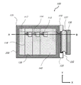
图1是本发明的实施方式1的液晶显示装置中的液晶面板的平面图。 1 is a plan view of a liquid crystal panel in a liquid crystal display device according to Embodiment 1 of the present invention.

图2是本发明的实施方式1的液晶显示装置中的液晶面板的剖视图。 2 is a cross-sectional view of a liquid crystal panel in the liquid crystal display device according to Embodiment 1 of the present invention.

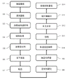
图3是表示本发明的实施方式1中的液晶面板的制造方法中的组装工序的流程图。 3 is a flowchart showing an assembly process in the method of manufacturing a liquid crystal panel in Embodiment 1 of the present invention.

图4是表示本发明的实施方式1的液晶面板制造工序中的母TFT基板以及母CF基板的平面图。 4 is a plan view showing a mother TFT substrate and a mother CF substrate in a liquid crystal panel manufacturing process according to Embodiment 1 of the present invention.

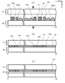
图5是表示本发明的实施方式1的液晶面板制造工序中的母TFT基板以及母CF基板的剖视图。 5 is a cross-sectional view showing a mother TFT substrate and a mother CF substrate in a liquid crystal panel manufacturing process according to Embodiment 1 of the present invention.

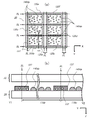
图6是表示本发明的实施方式1的液晶面板制造工序中的划线工序的母TFT基板以及母CF基板的平面图以及剖视图。 6 is a plan view and a cross-sectional view of a mother TFT substrate and a mother CF substrate showing a scribing step in the liquid crystal panel manufacturing process according to Embodiment 1 of the present invention.

图7是表示本发明的实施方式1的液晶面板制造工序中的划线工序以及单元分割工序的信号端子附近的剖视图。 7 is a cross-sectional view showing the vicinity of signal terminals in a scribing step and a cell division step in the liquid crystal panel manufacturing step according to Embodiment 1 of the present invention.

图8是表示本发明的实施方式1变形例的液晶面板制造工序中的母TFT基板以及母CF基板的剖视图。 8 is a cross-sectional view showing a mother TFT substrate and a mother CF substrate in a liquid crystal panel manufacturing process according to a modified example of Embodiment 1 of the present invention.

图9是表示本发明的实施方式1变形例的液晶面板制造工序中的划线工序的母TFT基板以及母CF基板的剖视图。 9 is a cross-sectional view of a mother TFT substrate and a mother CF substrate showing a scribing step in a liquid crystal panel manufacturing process according to a modified example of Embodiment 1 of the present invention.

图10是表示本发明的实施方式1变形例的液晶面板制造工序中的母TFT基板以及母CF基板的平面图以及剖视图。 10 is a plan view and a cross-sectional view showing a mother TFT substrate and a mother CF substrate in a liquid crystal panel manufacturing process according to a modified example of Embodiment 1 of the present invention.

图11是表示本发明的实施方式1变形例的液晶面板制造工序中的划线工序的母TFT基板以及母CF基板的平面图以及剖视图。 11 is a plan view and a cross-sectional view of a mother TFT substrate and a mother CF substrate showing a scribing step in a liquid crystal panel manufacturing process according to a modified example of Embodiment 1 of the present invention.

图12是本发明的实施方式2的液晶显示装置中的液晶面板的平面图。 12 is a plan view of a liquid crystal panel in a liquid crystal display device according to Embodiment 2 of the present invention.

图13是本发明的实施方式2的液晶显示装置中的液晶面板的剖视图。 13 is a cross-sectional view of a liquid crystal panel in a liquid crystal display device according to Embodiment 2 of the present invention.

图14是表示本发明的实施方式2的液晶面板制造工序中的母TFT基板以及母CF基板的剖视图。 14 is a cross-sectional view showing a mother TFT substrate and a mother CF substrate in a liquid crystal panel manufacturing process according to Embodiment 2 of the present invention.

图15是表示本发明的实施方式2变形例的液晶面板制造工序中的划线工序的母TFT基板以及母CF基板的剖视图。 15 is a cross-sectional view of a mother TFT substrate and a mother CF substrate showing a scribing step in a liquid crystal panel manufacturing process according to a modified example of Embodiment 2 of the present invention.

其中,附图标记说明如下: Wherein, the reference signs are explained as follows:

100、101 液晶面板、110、110a~110f TFT基板、120、120a~120f CF基板、10 母TFT基板、20 母CF基板、30 母单元基板、111、121 玻璃基板、112、122 取向膜、113 像素电极、114 TFT、115 绝缘膜、116 栅极布线、117 源极布线、118 信号端子、123 共同电极、124滤色片、125 BM、126 视差屏障、130、130a~130f 主密封图案、131、131ps、 132、 132ps 间隙保持件、132o 开口部、133 柱状隔离件、134、135 偏振片、136 控制基板、137 FFC 、140 液晶层、140dp 液晶材料、150a~150f、157 主密封剂、151、153 辅助密封剂、152 隔离件、154、156 密封剥离辅助层、155 不要部切断片、200、200a~200f 显示区域  SL 刻划线、WH 刀轮。 100, 101 LCD panel, 110, 110a~110f TFT substrate, 120, 120a~120f CF substrate, 10 mother TFT substrate, 20 mother CF substrate, 30 mother unit substrate, 111, 121 glass substrate, 112, 122 alignment film, 113 Pixel electrode, 114 TFT, 115 insulating film, 116 gate wiring, 117 source wiring, 118 signal terminal, 123 common electrode, 124 color filter, 125 BM, 126 parallax barrier, 130, 130a-130f main seal pattern, 131 . , 153 Auxiliary sealant, 152 Spacer, 154, 156 Sealing and peeling auxiliary layer, 155 Unnecessary cut-off piece, 200, 200a~200f Display area SL Score line, WH Cutter wheel.

具体实施方式 Detailed ways

实施方式1 Embodiment 1

使用图1以及图2的示意图,对本实施方式1的液晶显示装置中所使用的液晶面板100的结构进行说明。图1表示液晶面板整体的结构的平面图,图2表示图1中的A-B剖视线的剖视图。此外,此处,作为一例,对TFT(Thin Film Transistor:薄膜晶体管)方式的双画面显示器液晶面板进行说明。如图所示,该液晶面板100具有:开关元件基板(以下称为TFT基板110),将作为开关元件的TFT配置成阵列状;滤色片基板(以下称为CF基板120),形成有滤色片等;主密封图案130,相对于显示区域200在TFT基板110和CF基板120之间以至少包围显示区域200的方式配置且将CF基板120和TFT基板110之间的间隙密封,该显示区域200是与在液晶面板100动作时显示图像的显示面对应的区域。进而,在TFT基板110和CF基板120之间,在显示区域200内配置有很多使基板间形成并保持预定的一定范围的间隙的柱状隔离件133,换言之,在显示区域200内配置有很多使基板间的距离保持为一定范围的柱状隔离件133。在由该主密封图案130密封并且由柱状隔离件保持的CF基板120和TFT基板110之间的间隙的至少与显示区域200对应的区域夹持有液晶材料,从而配置有液晶层140。换言之,液晶材料被主密封图案130包围并密封。此处,作为液晶材料,采用一般的TN(Twisted Nematic:扭曲向列)型的液晶材料。此外,关于此处所使用的显示区域200,在液晶面板100的TFT基板110上、CF基板120上或者在两基板间夹持的区域都使用,在本说明书中,都以同样的意思来使用。 The structure of the liquid crystal panel 100 used in the liquid crystal display device of Embodiment 1 will be described with reference to the schematic diagrams of FIGS. 1 and 2 . FIG. 1 is a plan view showing the overall structure of a liquid crystal panel, and FIG. 2 is a cross-sectional view taken along the line A-B in FIG. 1 . In addition, here, as an example, a TFT (Thin Film Transistor: Thin Film Transistor) liquid crystal panel for a dual-screen display will be described. As shown in the figure, the liquid crystal panel 100 has: a switching element substrate (hereinafter referred to as TFT substrate 110 ), in which TFTs serving as switching elements are arranged in an array; a color filter substrate (hereinafter referred to as CF substrate 120 ), formed with filter Color chips and the like; the main seal pattern 130 is disposed between the TFT substrate 110 and the CF substrate 120 in the display region 200 so as to at least surround the display region 200 and seal the gap between the CF substrate 120 and the TFT substrate 110. The area 200 is an area corresponding to the display surface on which an image is displayed when the liquid crystal panel 100 is operating. Furthermore, between the TFT substrate 110 and the CF substrate 120, a large number of columnar spacers 133 are arranged in the display area 200 to form and maintain a predetermined gap between the substrates. The distance between the substrates is maintained as a certain range of columnar spacers 133 . A liquid crystal material is sandwiched between CF substrate 120 and TFT substrate 110 sealed by main seal pattern 130 and held by columnar spacers at least in a region corresponding to display region 200 , and liquid crystal layer 140 is disposed. In other words, the liquid crystal material is surrounded and sealed by the main seal pattern 130 . Here, as the liquid crystal material, a general TN (Twisted Nematic: twisted nematic) type liquid crystal material is used. In addition, the display region 200 used here is used on the TFT substrate 110 of the liquid crystal panel 100, on the CF substrate 120, or a region sandwiched between the two substrates, and they are used in the same meaning in this specification.

上述的TFT基板110具有如下等构件:取向膜112,在透明基板即由厚度为0.7mm左右的一般的玻璃构成的玻璃基板111的一个面使液晶取向;像素电极113,设置在取向膜112的下部,施加对液晶进行驱动的电压;作为向像素电极113供给电压的开关元件的TFTl14;绝缘膜115,覆盖TFTl14;作为向TFT114供给信号的布线的多个栅极布线116以及源极布线117;信号端子118,从外部接收向TFT114供给的信号;转移电极(transfer electrode)(省略图示),用于将从信号端子118输入的信号向对置电极123传递。另外,在玻璃基板111的另一个面具有偏振片134。 The above-mentioned TFT substrate 110 has the following components: an alignment film 112 for aligning liquid crystals on one surface of a transparent substrate, that is, a glass substrate 111 made of general glass with a thickness of about 0.7 mm; In the lower part, a voltage for driving the liquid crystal is applied; a TFT114 as a switching element supplying a voltage to the pixel electrode 113; an insulating film 115 covering the TFT114; a plurality of gate wirings 116 and source wirings 117 as wirings for supplying signals to the TFT114; The signal terminal 118 receives a signal supplied to the TFT 114 from the outside; a transfer electrode (not shown in the figure) is used to transmit the signal input from the signal terminal 118 to the counter electrode 123 . In addition, a polarizing plate 134 is provided on the other surface of the glass substrate 111 .

另一方面,上述的CF基板120具有如下等构件:取向膜122,在透明基板即由厚度为0.1mm左右的超薄玻璃构成的玻璃基板121的一个面使液晶取向;共同电极(common electrode)123,配置在取向膜122的下部,在与TFT基板110上的像素电极113之间产生电场,对液晶进行驱动;滤色片124,设置在共同电极123下部;黑矩阵(Black Matrix:BM)125,该黑矩阵是为了对滤色片124间进行遮光或对在与显示区域200对应的区域外侧所配置的边缘区域进行遮光而设置的遮光层。另外,在玻璃基板121的另一个面,作为双画面显示器,在与在像素内所配置的BM125错开的位置形成有将视野方向分离为二个方向的遮光层即视差屏障126。进而,在视差屏障126的外侧具有偏振片135。作为滤色片124,能够选择在树脂中分散了顔料等的色料(coloring material)层,起到有选择地使红、绿、蓝等特定波长范围的光透过的滤光片的功能,以这些不同颜色的色料层有规则地排列的方式构成。在滤色片124间以外,BM125还配置在显示区域200外侧的边缘区域,在CF基板120的边缘区域的大致整个区域形成,对在显示中不需要的边缘区域的CF基板120中的光的透过进行遮光。作为构成BM125以及视差屏障126的遮光层,能够选择使用了铬和氧化铬的层叠膜等的金属类的材料或在树脂中分散了黑色粒子的树脂类的材料等。此外,也可以做成如下结构:在取向膜的下层,以覆盖滤色片124和BM125的方式设置由透明树脂膜构成的覆盖层。 On the other hand, the above-mentioned CF substrate 120 has the following components: an alignment film 122 for aligning liquid crystals on one surface of a transparent substrate, that is, a glass substrate 121 made of ultra-thin glass with a thickness of about 0.1 mm; a common electrode (common electrode) 123, arranged at the lower part of the alignment film 122, generates an electric field between the pixel electrode 113 on the TFT substrate 110, and drives the liquid crystal; the color filter 124 is arranged at the lower part of the common electrode 123; black matrix (Black Matrix: BM) 125 , the black matrix is a light shielding layer provided for shielding between the color filters 124 or for shielding an edge region arranged outside the region corresponding to the display region 200 . In addition, on the other surface of the glass substrate 121, a parallax barrier 126, which is a light-shielding layer that separates the viewing direction into two directions, is formed at a position shifted from the BM 125 arranged in the pixel as a dual-screen display. Furthermore, a polarizing plate 135 is provided outside the parallax barrier 126 . As the color filter 124, a coloring material (coloring material) layer in which a pigment or the like is dispersed in the resin can be selected to function as a filter that selectively transmits light in a specific wavelength range such as red, green, and blue. It is formed in such a way that these colorant layers of different colors are regularly arranged. In addition to between the color filters 124, the BM 125 is also arranged in the edge area outside the display area 200, and is formed in substantially the entire area of the edge area of the CF substrate 120. Shade through. As the light-shielding layer constituting the BM 125 and the parallax barrier 126 , a metal-based material such as a laminate film using chromium and chromium oxide, a resin-based material in which black particles are dispersed in resin, or the like can be selected. In addition, a structure may be adopted in which a cover layer made of a transparent resin film is provided on the lower layer of the alignment film so as to cover the color filter 124 and the BM 125 .

另外,TFT基板110和CF基板120经由主密封图案130贴合在一起,由在显示区域200配置的柱状隔离件133保持为预定的基板间隔。进而,转移电极与共同电极123利用转移件而电连接在一起,从信号端子118输入的信号传递至共同电极123。关于转移件,也能够通过在主密封图案130中混合导电性的粒子等来代用而省略,在本实施方式中,使用混合了导电性的粒子等的主密封图案130,从图1可知,主密封图案130和共同电极123接触,所以,将转移电极以在俯视下与主密封图案130重叠的方式配置并且与主密封图案130接触而设置,由此,转移电极与共同电极123经由主密封图案130电连接在一起。除此之外,液晶面板100具有产生驱动信号的控制基板136、将控制基板136电连接于信号端子118的FFC(Flexible Flat Cable:软性扁平电缆)137、成为光源的背光单元(通常,与TFT基板110的外侧对置配置,TFT基板110的外侧是与成为显示面的CF基板120侧相反的一侧,但在此未图示)等,成为显示面的显示区域200的CF基板120的外侧的部分与这些构件一起容纳在开放的框体(未图示)中,构成本实施方式1的液晶显示装置。 In addition, the TFT substrate 110 and the CF substrate 120 are bonded together via the main seal pattern 130 , and a predetermined substrate spacing is maintained by the columnar spacers 133 arranged in the display region 200 . Furthermore, the transfer electrode and the common electrode 123 are electrically connected together by a transfer member, and the signal input from the signal terminal 118 is transmitted to the common electrode 123 . The transfer material can also be omitted by mixing conductive particles in the main seal pattern 130 instead. In this embodiment, the main seal pattern 130 mixed with conductive particles and the like is used. As can be seen from FIG. The seal pattern 130 is in contact with the common electrode 123, so the transfer electrode is arranged so as to overlap the main seal pattern 130 in plan view and is provided in contact with the main seal pattern 130, whereby the transfer electrode and the common electrode 123 pass through the main seal pattern. 130 are electrically connected together. In addition, the liquid crystal panel 100 has a control substrate 136 for generating drive signals, an FFC (Flexible Flat Cable) 137 for electrically connecting the control substrate 136 to the signal terminal 118, and a backlight unit (usually, The outer sides of the TFT substrate 110 are arranged facing each other, and the outer side of the TFT substrate 110 is the side opposite to the side of the CF substrate 120 that becomes the display surface, but not shown here), etc., and the CF substrate 120 that becomes the display area 200 of the display surface The outer part is housed in an open housing (not shown) together with these members, and constitutes the liquid crystal display device of the first embodiment.

接着,对本实施方式1的液晶面板100的特征部分即成为面板周边部的边缘区域的结构进行补充说明。在本实施方式1的液晶面板100中,如图1所示,在边缘区域的主密封图案130的外侧,设置有保持基板切断时的基板间距离(基板间间隙)的间隙保持件131。在本实施方式1中,如图1以及图2所示,以将面板间完全填埋的方式设置有间隙保持件131,利用与主密封图案130相同的树脂材料形成为一体。如图1所示,在所完成的液晶面板100中,间隙保持件131设置至CF基板120的基板端。 Next, a supplementary description will be given of the structure of the edge region that is the characteristic portion of the liquid crystal panel 100 of the first embodiment, which is the panel peripheral portion. In the liquid crystal panel 100 of Embodiment 1, as shown in FIG. 1 , a gap holder 131 is provided outside the main seal pattern 130 in the edge region to maintain the inter-substrate distance (inter-substrate gap) when the substrates are cut. In Embodiment 1, as shown in FIGS. 1 and 2 , gap holders 131 are provided so as to completely fill between the panels, and are formed integrally with the same resin material as the main seal pattern 130 . As shown in FIG. 1 , in the completed liquid crystal panel 100 , the gap holder 131 is provided to the substrate end of the CF substrate 120 .

如上述那样对结构进行了说明的本实施方式1的液晶显示装置以及液晶面板100如下那样动作。例如,当从控制基板136输入电信号时,对像素电极113以及共同电极123施加驱动电压,液晶层140中的液晶分子的方向与驱动电压匹配地发生变化。并且,背光单元发出的光经由TFT基板110、液晶层140以及CF基板120透过至观察者侧或者被遮挡,由此,在液晶面板100的显示区域200显示影像等。此外,本实施方式1的液晶显示装置是双画面显示器液晶面板,所以,经由CF基板120而透过的光被视察屏障126限制在两个方向的预定的角度方向的视角范围。具体地说,在显示面上,在图中的+X方向和-X方向这两个方向具有视角范围来显示影像等。另外,设定与两个方向的视角范围对应的显示像素,进行各自不同的影像显示,由此,对于两个方向的视角范围分别显示不同的影像,作为双画面显示器液晶面板发挥功能。另外,本实施方式1的液晶显示装置如上述那样在边缘区域具有特征结构,所以,尽管是对于外部应力的施加而在耐久性方面有问题的使用了超薄玻璃的双画面显示器液晶面板,也能够得到具有高的耐久性的双画面显示器液晶面板。 The liquid crystal display device and liquid crystal panel 100 of Embodiment 1, whose configurations have been described above, operate as follows. For example, when an electrical signal is input from the control substrate 136 , a driving voltage is applied to the pixel electrode 113 and the common electrode 123 , and the orientation of the liquid crystal molecules in the liquid crystal layer 140 changes in accordance with the driving voltage. In addition, the light emitted by the backlight unit is transmitted to the viewer's side through the TFT substrate 110 , the liquid crystal layer 140 , and the CF substrate 120 or is blocked, thereby displaying images and the like on the display area 200 of the liquid crystal panel 100 . In addition, since the liquid crystal display device of Embodiment 1 is a dual-screen display liquid crystal panel, the light transmitted through the CF substrate 120 is limited by the viewing barrier 126 to a range of viewing angles in predetermined angular directions in two directions. Specifically, on the display surface, images and the like are displayed in two directions, the +X direction and the −X direction in the figure, having viewing angle ranges. In addition, display pixels corresponding to viewing angle ranges in two directions are set to display different images, thereby displaying different images for the viewing angle ranges in two directions, and functioning as a dual-screen display liquid crystal panel. In addition, since the liquid crystal display device according to Embodiment 1 has the characteristic structure in the edge region as described above, even though it is a dual-screen display liquid crystal panel using ultra-thin glass that has problems in durability against the application of external stress, A dual-screen display liquid crystal panel having high durability can be obtained.

接着,对本实施方式1的液晶显示装置以及液晶面板100的制造方法进行说明。通常,液晶面板是从比最终形状大的母基板截取一个或多个液晶面板进行制造(多面取出)的。此处,在本发明中以特征的组装工序为中心进行说明,作为一例,对从母基板截取6个液晶面板的情况进行说明。下面,根据图3所示的流程图对本实施方式1的液晶面板100的组装工序进行说明,并且,适当使用图4~图7的详细说明附图对特征工序进行说明。 Next, a method of manufacturing the liquid crystal display device and the liquid crystal panel 100 of the first embodiment will be described. Usually, a liquid crystal panel is manufactured by cutting out one or more liquid crystal panels from a mother substrate larger than the final shape (multi-sided extraction). Here, the present invention will be described centering on the characteristic assembling process, and a case where six liquid crystal panels are cut out from a mother substrate will be described as an example. Next, the assembly process of the liquid crystal panel 100 according to Embodiment 1 will be described based on the flowchart shown in FIG. 3 , and the characteristic steps will be described using the detailed description drawings of FIGS. 4 to 7 as appropriate.

首先,在基板准备工序中,准备彼此贴合前的截取TFT基板110的母TFT基板10和截取CF基板120的母CF基板20(S1)。关于母TFT基板10和母CF基板20,CF基板120最终因对玻璃进行薄型化加工而形成为超薄玻璃,但是,为了以后的工序的实施变得容易,直到中途为止,利用由厚度为0.5~1.5mm左右的玻璃构成的母TFT基板10和母CF基板20制造。此处,母TFT基板10和母CF基板20这两者都作为由厚度0.7mm的玻璃构成的基板来准备。图4(a)以及图4(b)分别表示在以后说明的贴合工序(S7)之前的阶段的母TFT基板10和母CF基板20,该贴合工序(S7)是将母TFT基板10和母CF基板20贴合的工序。 First, in the substrate preparation process, the mother TFT substrate 10 , which cuts out the TFT substrate 110 , and the mother CF substrate 20 , which cuts out the CF substrate 120 , are prepared before they are bonded together ( S1 ). Regarding the mother TFT substrate 10 and the mother CF substrate 20, the CF substrate 120 is finally formed into an ultra-thin glass by thinning the glass. The mother TFT substrate 10 and the mother CF substrate 20 made of glass with a diameter of about 1.5 mm are manufactured. Here, both the mother TFT substrate 10 and the mother CF substrate 20 were prepared as substrates made of glass with a thickness of 0.7 mm. 4( a ) and FIG. 4( b ) respectively show the mother TFT substrate 10 and the mother CF substrate 20 at the stage before the bonding process ( S7 ) described later. The bonding process ( S7 ) is to bond the mother TFT substrate 10 A step of bonding to the mother CF substrate 20 .

首先,如图4(a)所示,在母TFT基板10上制作6个TFT基板110a~110f,在以后进行的工序中,TFT基板110a~110f从母TFT基板10截取。进而,例如,在TFT基板110a上,如在结构的说明中所说明的那样,制作从外部接收信号的信号端子118、位于与液晶面板完成时的显示面对应的区域即显示区域200a的驱动液晶的像素电极113、TFT114、栅极布线116以及源极布线117等(在图4(a)中都省略图示)。另外,作为特征结构,在显示区域200a和信号端子118之间的区域的TFT基板110a表面,配置有密封剥离辅助层154。该密封剥离辅助层154设置在与沿着图4(b)中的CF基板120a的切断端部的位置对应的TFT基板110a表面,在切断CF基板120a时发挥效果,但是,关于密封剥离辅助层154的作用,在以后的制造方法的说明详细地说明,故在此省略说明。另外,关于TFT基板110b~110f,也省略图示以及说明,但是,制作与开关元件基板110a同样的结构。此外,这些信号端子118以及TFT114等的制作与一般的液晶面板中的TFT基板的制造方法同样即可,故省略关于详细的制造方法的说明。 First, as shown in FIG. 4( a ), six TFT substrates 110 a to 110 f are produced on the mother TFT substrate 10 , and the TFT substrates 110 a to 110 f are cut from the mother TFT substrate 10 in subsequent steps. Furthermore, for example, on the TFT substrate 110a, as described in the description of the structure, the signal terminal 118 for receiving a signal from the outside, and the driver of the display area 200a, which is an area corresponding to the display surface when the liquid crystal panel is completed, are formed. The pixel electrode 113 of the liquid crystal, the TFT 114 , the gate wiring 116 , the source wiring 117 , and the like (all are omitted in FIG. 4( a )). In addition, as a characteristic structure, on the surface of the TFT substrate 110 a in the region between the display region 200 a and the signal terminal 118 , the sealing and peeling auxiliary layer 154 is disposed. The sealing and peeling auxiliary layer 154 is provided on the surface of the TFT substrate 110a corresponding to the position along the cut end of the CF substrate 120a in FIG. The function of 154 will be described in detail in the description of the manufacturing method later, so the description is omitted here. In addition, although illustration and description are abbreviate|omitted about TFT substrate 110b-110f, the same structure as the switching element substrate 110a is produced. In addition, since the manufacturing method of these signal terminals 118, TFT 114, etc. is the same as the manufacturing method of the TFT substrate in a general liquid crystal panel, description about a detailed manufacturing method is abbreviate|omitted.

另一方面,如图4(b)所示,在母CF基板20上制作6个CF基板120a~120f,在以后进行的工序中,CF基板120a~120f从母CF基板20截取。进而,例如,在CF基板120a上,如在结构的说明中所说明的那样,在与液晶面板100完成时的显示面对应的区域即显示区域200,制作驱动液晶的共同电极123、滤色片124、BM125、柱状隔离件133(都省略图示)等。此外,这些共同电极123、滤色片124、BM125以及柱状隔离件133等的制作与一般的液晶面板中的滤色片基板的制造方法同样即可,故省略关于详细的制造方法的说明。 On the other hand, as shown in FIG. 4( b ), six CF substrates 120 a to 120 f are fabricated on the mother CF substrate 20 , and the CF substrates 120 a to 120 f are cut from the mother CF substrate 20 in subsequent steps. Furthermore, for example, on the CF substrate 120a, as described in the description of the structure, in the display area 200, which is an area corresponding to the display surface of the liquid crystal panel 100 when it is completed, a common electrode 123 for driving liquid crystals, a color filter, etc. are formed. Sheet 124 , BM 125 , columnar spacer 133 (both are not shown in the figure), and the like. The common electrode 123 , color filter 124 , BM 125 , columnar spacer 133 , and the like can be fabricated in the same way as the color filter substrate in a general liquid crystal panel, and thus detailed description of the fabrication method is omitted.

接着,在基板清洗工序中,对上述说明的那样准备的形成有TFT基板110a~110f的母TFT基板10进行清洗(S2)。接着,在取向膜材料涂敷工序中,在母TFT基板10的一个面涂敷形成取向膜材料(S3)。在该工序中,例如利用印刷法涂敷由有机膜构成的取向膜材料,利用加热板等进行烧结处理并使其干燥。然后,在摩擦研磨(rubbing)工序中对取向膜材料进行摩擦研磨,对取向膜材料表面进行取向处理,做成取向膜112(S4)。 Next, in the substrate cleaning step, the mother TFT substrate 10 on which the TFT substrates 110 a to 110 f are formed prepared as described above is cleaned ( S2 ). Next, in the alignment film material application step, an alignment film material is applied on one surface of the mother TFT substrate 10 ( S3 ). In this step, for example, an alignment film material made of an organic film is applied by a printing method, followed by firing treatment on a hot plate or the like and drying. Then, in a rubbing process, the alignment film material is rubbed and polished, and the surface of the alignment film material is subjected to an alignment treatment to form an alignment film 112 ( S4 ).

另外,与S2~S4同样地,对形成有CF基板120a~120f的母CF基板20也进行清洗、取向膜材料的涂敷、摩擦研磨,由此,形成取向膜122。接着,在密封剂涂敷工序中,将密封剂作为印刷膏利用丝网印刷装置在母TFT基板10或母CF基板20的一个面涂敷密封剂,最终形成包围显示区域200的形状的主密封图案130a~130f和在主密封图案130a~130f的外侧配置的成为间隙保持件131的密封剂(S5)。 Also, in the same manner as in S2 to S4 , the mother CF substrate 20 on which the CF substrates 120 a to 120 f are formed is also cleaned, coated with an alignment film material, and rubbed, thereby forming the alignment film 122 . Next, in the sealant application process, the sealant is applied as a printing paste on one surface of the mother TFT substrate 10 or the mother CF substrate 20 by a screen printing device, and finally a main seal having a shape surrounding the display area 200 is formed. The patterns 130 a to 130 f and the sealant to be the gap holder 131 arranged outside the main seal patterns 130 a to 130 f ( S5 ).

 具体地说,例如,如图4(b)所示,在形成于母CF基板20的CF基板120a~120f上形成有:主密封剂150a~150f,形成为包围各显示区域200a~200f的形状,具有之后包围密封液晶材料的多个密封区域;辅助密封剂(dummy sealant)151,沿着主密封剂150a~150f的外侧的各边配置。另外,关于辅助密封剂151,与CF基板120a~120f的外形一致地配置,即,与在将CF基板120a~120f从母CF基板20切出时的切断线上一致地配置。另外,这些主密封图案130a~130f和间隙保持件131由相同的密封剂形成,将该共同的密封剂作为印刷膏利用丝网印刷装置同时涂敷形成。此外,使构成主密封图案130a~130f和间隙保持件131的密封剂共同化,利用丝网印刷装置同时形成,由此,在不特别增加制造工序的情况下就能够配置间隙保持件131,因此,在本实施方式1中采用了丝网印刷。但是,在使用了利用喷嘴进行的涂敷(分配器法)的情况下,因耗费了用于涂敷形成间隙保持件131的喷嘴的移动时间也会导致增加一些处理时间,但是,通过使密封剂共同化而不会增加密封剂更换时间等这样长的处理时间,就能够配置间隙保持件131。 Specifically, for example, as shown in FIG. 4( b ), on the CF substrates 120 a to 120 f formed on the mother CF substrate 20 , main sealants 150 a to 150 f are formed in a shape surrounding each display area 200 a to 200 f , having a plurality of sealing regions surrounding and sealing the liquid crystal material; the auxiliary sealant (dummy sealant) 151 is arranged along each side of the outer sides of the main sealants 150a-150f. In addition, the auxiliary sealant 151 is arranged to match the outer shapes of the CF substrates 120 a to 120 f , that is, to match the cutting line when the CF substrates 120 a to 120 f are cut out from the mother CF substrate 20 . In addition, these main seal patterns 130a to 130f and the gap holder 131 are formed of the same sealant, and the common sealant is applied and formed simultaneously as a printing paste by a screen printing device. In addition, the sealants constituting the main seal patterns 130a to 130f and the gap holder 131 are made common and formed simultaneously by a screen printing device, so that the gap holder 131 can be arranged without particularly increasing the manufacturing process. , in the first embodiment, screen printing is used. However, in the case of using nozzle coating (dispenser method), the time spent moving the nozzle for coating to form the gap holder 131 also increases the processing time. However, by making the seal The gap holder 131 can be arranged without increasing the processing time such as the replacement time of the sealant by commonizing the agent.

接着,在液晶滴下工序中,在母TFT基板10或者母CF基板20的一个面,在由主密封剂150a~150f包围的区域内滴下很多液滴状的液晶材料140dp(S6)。具体地说,例如,如图4(b)所示,在母CF基板20的各CF基板120a~120f上,在由主密封剂150a~150f包围并密封液晶材料的密封区域内,以整体形成预定量的液晶层140的方式滴下很多液滴状的液晶材料140dp。另外,此处,将使用所谓的滴下注入(ODF:One Drop Filling)法填充液晶来形成液晶层140的方法作为一例,所以这样形成,但是,在使用所谓的真空注入法的情况下,主密封剂150a~150f不是完全封闭的形状,形成有一部分开口的液晶注入口。进而,关于沿着主密封剂150a~150f的外侧的各边配置的辅助密封剂151,沿着除了液晶注入口之外的主密封剂150a~150f的外侧形成。此外,在使用真空注入法的情况下,理所当然,由于在贴合后从所述液晶注入口注入液晶材料,所以,省略上述说明的液滴状的液晶材料140dp的形成处理。 Next, in the liquid crystal dropping step, a large number of droplet-shaped liquid crystal material 140dp is dropped on one surface of the mother TFT substrate 10 or the mother CF substrate 20 in a region surrounded by the main sealants 150a to 150f ( S6 ). Specifically, for example, as shown in FIG. 4( b ), on each of the CF substrates 120 a to 120 f of the mother CF substrate 20 , in the sealing region surrounded and sealed with the liquid crystal material by the main sealant 150 a to 150 f , integrally formed A predetermined amount of liquid crystal material 140dp is dropped in the form of liquid crystal layer 140 . In addition, here, a so-called drop filling (ODF: One Drop Filling) method is used to fill the liquid crystal to form the liquid crystal layer 140 as an example, so it is formed in this way, but in the case of using the so-called vacuum filling method, the main seal The agents 150a to 150f are not in a completely closed shape, but form a partially opened liquid crystal injection port. Furthermore, the auxiliary sealant 151 arranged along each outer side of the main sealant 150a to 150f is formed along the outer side of the main sealant 150a to 150f except for the liquid crystal injection port. In the case of using the vacuum injection method, of course, the liquid crystal material is injected from the liquid crystal injection port after bonding, so the above-described formation process of the liquid crystal material 140dp in the form of droplets is omitted.

接着,在贴合工序中,将母TFT基板10与母CF基板20贴合,形成单元基板(S7)。具体地说,将如图4(a)以及图4(b)那样准备的母TFT基板10和母CF基板20以TFT基板110a~110f和CF基板120a~120f分别对应的方式对置配置,在真空中使两者接近并贴合。图5是表示S7以后的制造工序的剖视图,示出图4(b)的母CF基板20的剖视线YI-Y2的剖面,表示S7以后的制造工序中的CF基板120a和TFT基板110a的边缘区域的状况。如图5(a)那样,在母TFT基板10和母CF基板20贴合前的状态下,在相邻配置的CF基板120a和CF基板120c之间(相当于CF基板120a和CF基板120c被分离切断时的切断线上),在主密封剂150a和主密封剂150c之间形成有辅助密封剂151,在CF基板120a的与CF基板120c相邻的一侧相反的一侧的端部,在主密封剂150a的外侧仅配置有辅助密封剂151(相当于CF基板120a和母CF基板20的周边不要部玻璃被分离切断时的切断线上)。 Next, in the bonding step, the mother TFT substrate 10 and the mother CF substrate 20 are bonded to form a unit substrate ( S7 ). Specifically, mother TFT substrate 10 and mother CF substrate 20 prepared as shown in FIG. 4( a ) and FIG. The two are brought close and bonded in a vacuum. 5 is a cross-sectional view showing the manufacturing process after S7, showing the cross-sectional line YI-Y2 of the mother CF substrate 20 in FIG. The condition of the area. As shown in FIG. 5( a ), in the state before the mother TFT substrate 10 and the mother CF substrate 20 are bonded, between the CF substrate 120a and the CF substrate 120c arranged adjacently (equivalent to the CF substrate 120a and the CF substrate 120c being Cutting line at the time of separation and cutting), the auxiliary sealant 151 is formed between the main sealant 150a and the main sealant 150c, and at the end of the CF substrate 120a opposite to the side adjacent to the CF substrate 120c, Only the auxiliary sealant 151 is disposed outside the main sealant 150 a (corresponding to a cutting line when the unnecessary peripheral glass of the CF substrate 120 a and the mother CF substrate 20 is separated and cut).

这样对置配置的母TFT基板10和母CF基板20在图5(a)中的箭头方向上接近,如图5(b)那样贴合。其结果是,主密封剂150a、150c和辅助密封剂151被母TFT基板10和母CF基板20夹压变形而扩展,在主密封剂150a和主密封剂150c的相邻部分,主密封剂150a、主密封剂150c以及辅助密封剂151被一体化,形成主密封图案130a、主密封图案130c以及间隙保持件131。另外,在与相邻的一侧相反的一侧的端部,主密封剂150a和辅助密封剂151被一体化,形成主密封图案130a和间隙保持件131。另外,在辅助密封剂151中混入的隔离件152优选使用例如玻璃的圆柱状的隔离件(称为微细杆(micro-rod)等),但是,在辅助密封剂151被按压变形时,由该隔离件152保持母TFT基板10和母CF基板20间的基板间隔,将辅助密封剂151按压变形而形成的间隙保持件131有助于保持母TFT基板10和母CF基板20间的基板间隔。此外,关于在辅助密封剂151中混入的隔离件152,只要是将基板间的距离(基板间间隙)保持为一定范围的隔离件,就能够得到同样的效果,不限于圆柱状玻璃,也可以是球状的隔离件。关于材质,也不限于玻璃这样的变形少的硬质的材质,即使是比较硬的弹性体(例如,丙烯酸树脂)等的在预定的压力范围内伴有一定范围内的变形的材质,也能够具有将基板间隔(基板间距离)保持为一定范围的功能,因而能够进行置换。 Mother TFT substrate 10 and mother CF substrate 20 arranged so as to face each other approach in the direction of the arrow in FIG. 5( a ), and are bonded together as shown in FIG. 5( b ). As a result, the main sealant 150a, 150c and the auxiliary sealant 151 are expanded by being pinched and deformed by the mother TFT substrate 10 and the mother CF substrate 20, and in the adjacent part of the main sealant 150a and the main sealant 150c, the main sealant 150a , the main sealant 150c and the auxiliary sealant 151 are integrated to form the main seal pattern 130a, the main seal pattern 130c and the gap holder 131. In addition, at the end portion on the side opposite to the adjacent side, the main sealant 150 a and the auxiliary sealant 151 are integrated to form the main seal pattern 130 a and the gap holder 131 . In addition, as the spacer 152 mixed in the auxiliary sealant 151, it is preferable to use, for example, a cylindrical spacer of glass (called a micro-rod (micro-rod) or the like), but when the auxiliary sealant 151 is pressed and deformed, due to this The spacer 152 maintains the substrate gap between the mother TFT substrate 10 and the mother CF substrate 20 , and the gap holder 131 formed by pressing and deforming the auxiliary sealant 151 helps maintain the substrate gap between the mother TFT substrate 10 and the mother CF substrate 20 . In addition, the same effect can be obtained as long as the spacer 152 mixed in the auxiliary sealant 151 maintains the distance between the substrates (inter-substrate gap) within a certain range, and it is not limited to cylindrical glass. It is a spherical spacer. Regarding the material, it is not limited to a hard material with little deformation such as glass, even a material that is accompanied by a certain range of deformation within a predetermined pressure range such as a relatively hard elastic body (for example, acrylic resin). It has the function of keeping the board spacing (distance between boards) within a certain range, so it can be replaced.

接着,在密封剂硬化工序中,在将母TFT基板10和母CF基板20贴合的状态下,使主密封剂150a~150f或者辅助密封剂151等的在母TFT基板10和母CF基板20间形成的密封剂完全硬化(S8)。例如,与密封剂的材质相匹配地进行加热或照射紫外线来进行该工序。在本实施方式1中,利用与滴下注入法相配性好的照射紫外线的方法进行硬化。利用该工序,母TFT基板10和母CF基板20在保持对位的位置关系不变的状态下被固定。 Next, in the sealant hardening step, in the state where the mother TFT substrate 10 and the mother CF substrate 20 are bonded together, the main sealants 150a to 150f or the auxiliary sealant 151 are placed on the mother TFT substrate 10 and the mother CF substrate 20. The sealant formed in between hardens completely (S8). For example, this step is performed by heating or irradiating ultraviolet rays according to the material of the sealant. In Embodiment 1, curing is performed by irradiating ultraviolet rays, which is compatible with the drop injection method. Through this process, the mother TFT substrate 10 and the mother CF substrate 20 are fixed while maintaining the positional relationship of the alignment.

另外,为了使液晶面板100轻量化或如本实施方式那样形成双画面显示器液晶面板而将构成TFT基板10和CF基板20的玻璃基板的至少一个薄型化加工为超薄玻璃的情况下,在该贴合的状态下实施即可,在本实施方式1中实施薄型化研磨工序(S9)。具体地说,能够选择利用药液或机械研磨进行的薄型化处理,但是,在使用由在基板厚度控制性方面适合超薄玻璃加工的药液进行的薄型化处理的情况下,在使TFT基板10和CF基板20这两者薄型化时,在对母TFT基板10和母CF基板20的周边部实施防止药液进入基板间的周边密封后,将贴合的母TFT基板10和母CF基板20整体浸渍在药液中,对母TFT基板10和母CF基板20的表面进行切削薄型化。另外,若仅使TFT基板10和CF基板20中的一个、如本实施方式1那样仅使CF基板20薄型化,则除了周边密封之外,在母TFT基板10表面利用抗蚀剂等形成保护层的状态下,仅对母CF基板20的表面进行切削薄型化即可。其结果是,如图5(c)那样,能够得到仅将母CF基板20薄型化加工为0.1mm左右的超薄玻璃的单元基板。 In addition, when at least one of the glass substrates constituting the TFT substrate 10 and the CF substrate 20 is thinned and processed into ultra-thin glass in order to reduce the weight of the liquid crystal panel 100 or to form a dual-screen display liquid crystal panel as in this embodiment, the What is necessary is just to implement in the bonded state, and in this Embodiment 1, implement a thinning grinding process (S9). Specifically, it is possible to select a thinning treatment using a chemical solution or mechanical polishing. However, in the case of using a thinning treatment performed by a chemical solution suitable for ultra-thin glass processing in terms of substrate thickness controllability, the TFT substrate 10 and the CF substrate 20 are both thinned, after the periphery of the mother TFT substrate 10 and the mother CF substrate 20 is sealed to prevent the chemical solution from entering between the substrates, the bonded mother TFT substrate 10 and mother CF substrate 20 is immersed in the chemical solution as a whole, and the surfaces of the mother TFT substrate 10 and the mother CF substrate 20 are cut and thinned. In addition, if only one of the TFT substrate 10 and the CF substrate 20 is made thinner as in the first embodiment, only the CF substrate 20 is thinned. In addition to peripheral sealing, the surface of the mother TFT substrate 10 is protected by a resist or the like. In the state of layers, only the surface of the mother CF substrate 20 may be thinned by cutting. As a result, as shown in FIG. 5( c ), it is possible to obtain an ultrathin glass cell substrate by processing only the mother CF substrate 20 to a thickness of about 0.1 mm.

进而,进行如下的视差屏障形成工序:在该被薄型化的母CF基板20侧的表面形成作为双画面显示器液晶面板而发挥功能的结构即由遮光层构成的视差屏障126(S10)。具体地说,根据构成视差屏障126的材料,将使用了铬和氧化铬的层叠膜等的金属类的材料或在树脂中分散了黑色粒子的树脂类的材料进行成膜,对用于起到视差屏障126功能的预定的位置具有开口部的形状实施与构成各个视差屏障126的材料对应的图案加工。如以上那样,形成母单元基板30。 Furthermore, a parallax barrier forming step of forming a parallax barrier 126 made of a light-shielding layer that functions as a dual-screen display liquid crystal panel is performed on the surface of the thinned mother CF substrate 20 ( S10 ). Specifically, depending on the material constituting the parallax barrier 126, a metal-based material such as a laminated film using chromium and chromium oxide, or a resin-based material in which black particles are dispersed in a resin is formed into a film to provide a The predetermined position of the parallax barrier 126 function has a shape of an opening, and pattern processing is performed corresponding to the material constituting each parallax barrier 126 . As above, the mother unit substrate 30 is formed.

接着,在划线工序中,对如上那样形成的母单元基板30,在母TFT基板10和母CF基板20各自的表面形成成为切断的起点的线形状的切痕(称为刻划线)(S11)。通常,就玻璃基板的切断而言,在玻璃基板的表面形成成为切断的起点的刻划线之后,在刻划线的附近施加应力,从而进行分割。 Next, in the scribing step, on the mother unit substrate 30 formed as described above, a line-shaped cut (referred to as a scribe line) to be a starting point of cutting is formed on the respective surfaces of the mother TFT substrate 10 and the mother CF substrate 20 ( S11). Usually, in cutting a glass substrate, after forming a scribe line which becomes a cutting start point on the surface of a glass substrate, stress is applied to the vicinity of a scribe line, and division|segmentation is performed.

对本实施方式1中的能够得到特征效果的划线工序,使用图6详细地进行说明。图6(a)是母单元基板30的平面图,图6(b)是表示图6(a)中的剖视线Y1-Y2(与图4(b)的剖视线Y1-Y2位置一致)的剖面。刻划线对应于母TFT基板10和母CF基板20各自的切断线而形成,在图6(a)中,图示了在由在本实施方式1中成为问题的超薄玻璃构成的母CF基板20上所形成的刻划线SL的位置。此外,在图6(a)以及图6(b)中,关于已经在母CF基板20表面形成的视差屏障26,是具有相对于由超薄玻璃构成的母CF基板20的厚度能够忽略程度的厚度、并且对基板强度的帮助也是几乎能够忽略的结构,故省略图示以及视差屏障26对切断的帮助等的说明。 The scribing step for obtaining the characteristic effect in Embodiment 1 will be described in detail with reference to FIG. 6 . 6( a ) is a plan view of the mother unit substrate 30 , and FIG. 6( b ) is a cross section showing the cross-sectional line Y1-Y2 in FIG. 6( a ) (the position coincides with the cross-sectional line Y1-Y2 in FIG. 4( b ). . Scribe lines are formed corresponding to the cutting lines of the mother TFT substrate 10 and the mother CF substrate 20, and FIG. The position of the scribe line SL formed on the substrate 20 . In addition, in FIG. 6( a ) and FIG. 6( b ), the parallax barrier 26 already formed on the surface of the mother CF substrate 20 is negligible with respect to the thickness of the mother CF substrate 20 made of ultra-thin glass. The thickness and the contribution to the strength of the substrate are also almost negligible structures, so illustrations and descriptions of the contribution of the parallax barrier 26 to cutting and the like are omitted.

 如图6(b)所示,利用划线刀的刀轮WH形成刻划线SL,但是,在由特别成为问题的超薄玻璃构成的母CF基板20的刻划线SL形成部分,在刻划线SL上,在母CF基板20下层,配置有将母CF基板20和母TFT基板10的基板间距离保持为一定范围的间隙保持件131。因此,在为了形成切痕而将刀轮WH按压在母CF基板20表面时,由0.1mm左右的超薄玻璃构成的母CF基板20也由间隙保持件131保持而不会挠曲,针对刀轮WH的按压的回弹力也稳定。其结果是,刀轮WH在母CF基板20表面的旋转和利用旋转而被推进的刀轮WH扫掠(scanning)稳定,能够形成稳定的刻划线SL。进而,由于能够形成稳定的刻划线SL,所以,能够对在以后说明的单元分割工序中通过切断而得到的超薄玻璃端面残存微小裂纹等的切断损伤以及在切断时产生裂开等的不良进行抑制。另外,在本实施方式1中,在刀轮WH被按压的刻划线SL附近,在刻划线SL正下方配置的间隙保持件131填埋直到形成有在刻划线SL的两侧配置的主密封图案130a或主密封图案130c的区域而形成,换言之,得到间隙保持件131与在刻划线SL的两侧配置的主密封图案130a或者主密封图案130c形成为一体的结构,所以,在刻划线SL附近,利用这些一体化的结构整体保持母CF基板20,能够最大地发挥保持母CF基板20的作用,关于上述说明的保持母CF基板20发挥作用而得到的几个效果,也能够最大限度地得到。另外,在不存在相邻的面板的基板端的例如图6(b)的左侧的刻划线SL的下部,间隙保持件131和主密封图案130a也一体化配置,当然,也能够得到由间隙保持件131保持母CF基板20的作用,并且,也能够得到利用使间隙保持件131和主密封图案130a一体化后的结构而得到的作用以及附加效果。 As shown in FIG. 6( b ), the scribe line SL is formed by the cutter wheel WH of the scribe blade. On the scribe line SL, on the lower layer of the mother CF substrate 20, a gap holder 131 is arranged to keep the inter-substrate distance between the mother CF substrate 20 and the mother TFT substrate 10 within a certain range. Therefore, when the cutter wheel WH is pressed against the surface of the mother CF substrate 20 to form a cut, the mother CF substrate 20 made of ultra-thin glass of about 0.1 mm is also held by the gap holder 131 without bending. The repulsion force of the pressing of the wheel WH is also stable. As a result, the rotation of the cutter wheel WH on the surface of the mother CF substrate 20 and the scanning of the cutter wheel WH propelled by the rotation are stabilized, and stable scribe lines SL can be formed. Furthermore, since a stable scribe line SL can be formed, cutting damage such as microcracks remains on the end surface of the ultra-thin glass obtained by cutting in the unit division step described later, and defects such as cracks can occur during cutting. to suppress. In addition, in the first embodiment, near the scribe line SL on which the cutter wheel WH is pressed, the gap holders 131 arranged directly below the scribe line SL are buried until the gap holders 131 arranged on both sides of the scribe line SL are formed. The main seal pattern 130a or the main seal pattern 130c is formed in the area of the main seal pattern 130c. In other words, the structure in which the gap holder 131 is integrally formed with the main seal pattern 130a or the main seal pattern 130c arranged on both sides of the scribe line SL is obtained. In the vicinity of the scribe line SL, these integrated structures are used to hold the mother CF substrate 20 as a whole, so that the function of holding the mother CF substrate 20 can be maximized. Regarding the effects obtained by holding the mother CF substrate 20 described above, there are also be able to get as much as possible. In addition, the gap holder 131 and the main seal pattern 130a are also integrally arranged at the lower part of the substrate end where there is no adjacent panel, for example, the scribe line SL on the left side of FIG. 6( b ). The holder 131 has the function of holding the mother CF board 20 , and the function and additional effect obtained by the structure in which the gap holder 131 and the main seal pattern 130 a are integrated can also be obtained.

接着,在单元分割工序中,将单元基板分割为很多独立单元基板(S12)。在该工序中,在先前说明的划线工序S11中形成的刻划线SL附近施加应力,由此,按各个独立单元基板的TFT基板110a~110f和CF基板120a~120f的形状进行分割,从母单元基板30被分割为独立单元基板。如先前说明的那样,就在划线工序S11中形成的刻划线SL而言,能够形成稳定的刻划线SL,由此,在刻划线SL附近,很少会发生微小裂纹,刻划线SL的直线性也良好,所以,能够抑制在该单元分割工序中通过切断而得到的CF基板120a~120f的超薄玻璃端面残存微小裂纹等的切断损伤以及在切断时发生裂开等的不良。 Next, in the unit dividing step, the unit substrate is divided into a plurality of independent unit substrates ( S12 ). In this step, stress is applied near the scribe line SL formed in the scribing step S11 described above, whereby the TFT substrates 110a to 110f and the CF substrates 120a to 120f of the individual unit substrates are divided according to the shapes of the individual unit substrates. The mother unit substrate 30 is divided into individual unit substrates. As described above, with regard to the scribe line SL formed in the scribing step S11, a stable scribe line SL can be formed, whereby microcracks rarely occur in the vicinity of the scribe line SL, and the scribe line SL is seldom generated. The linearity of the line SL is also good, so that the CF substrates 120a to 120f obtained by cutting in the unit division step can be suppressed from cutting damage such as microcracks remaining on the end faces of the ultra-thin glass and from causing defects such as cracks during cutting. .

此处,关于先前使用图4(a)所说明的在母TFT基板10表面形成的密封剥离辅助层154的作用,适当地使用图7详细地进行说明。密封剥离辅助层154在该单元分割工序S12中起到重要的作用。由于TFT基板110a~110f的信号端子118需要被露出,所以,与信号端子118对置的部分的母CF基板20在该分割工序中作为不要部而被除去。但是,在本实施方式1中,如在图6中所说明的那样,在与各CF基板120a~120f的基板端对应地形成的划刻线SL的下部,配置有间隙保持件131。 Here, the function of the sealing and peeling auxiliary layer 154 formed on the surface of the mother TFT substrate 10 described above using FIG. 4( a ) will be described in detail using FIG. 7 as appropriate. The sealing and peeling auxiliary layer 154 plays an important role in this unit dividing step S12. Since the signal terminals 118 of the TFT substrates 110 a to 110 f need to be exposed, portions of the mother CF substrate 20 facing the signal terminals 118 are removed as unnecessary portions in this dividing step. However, in Embodiment 1, as described in FIG. 6 , gap holders 131 are disposed below the scribe lines SL formed corresponding to the substrate ends of the CF substrates 120a to 120f.

在图7中,作为一例,示出TFT基板110a的信号端子118附近,与图6(a)中的剖视线X1-X2的剖面对应。如图7(a)所示,特别是在配置信号端子118的一侧的基板端所形成的刻划线SL的下部,也横跨刻划线SL的两侧而配置有间隙保持件131。间隙保持件131在本实施方式1中由密封剂形成,粘接在母TFT基板10和母CF基板20这两者的表面而形成。因此,与信号端子118对置的母CF基板20的不要部(在图7(a)中,作为不要部切断片155而示出。)也经由间隙保持件131固定于母TFT基板10。因此,即使该不要部切断片155从CF基板120a被分割,仍与母TFT基板10(或者各个TFT基板110a等)固定,不能够分离除去。在假设由外力等强制分离的情况下,TFT基板110a表面的膜固定在不要部切断片155上而被剥离。例如,向信号端子118的引出布线等与不要部切断片155一起被剥离。但是,在本实施方式1中,在经由间隙保持件131固定有该母CF基板20的不要部切断片155的TFT基板110a等的表面,配置有密封剥离辅助层154。该密封剥离辅助层154具有帮助构成间隙保持件131的密封剂从TFT基板110a~110f剥离的作用,例如,由彼此紧贴力小的二层膜或包含该二层膜的多层膜等构成。更具体地说,能够使用在a-Si膜上形成了硅氮化膜的二层膜等。在这样的层结构的情况下,在密封剥离辅助层154的形成区域那样的1边由以毫米为单位的比较大的连续图案构成时,彼此的层间的紧贴力变小,能够容易在层间进行剥离。因此,在单元分割工序S12中作为密封剥离辅助层154发挥功能的情况下,如图7(b)所示,密封剥离辅助层154的上层膜(作为密封剥离辅助层154而示出)保持与间隙保持件131固定的状态从TFT基板110a分离,密封剥离辅助层154的下层膜(作为密封剥离辅助层156而示出。)残留在TFT基板110a~110f上,能够防止其他结构被剥离等的对TFT基板110a~110f造成损伤。 In FIG. 7 , as an example, the vicinity of the signal terminal 118 of the TFT substrate 110 a is shown, which corresponds to the cross-section taken along the cross-sectional line X1 - X2 in FIG. 6( a ). As shown in FIG. 7( a ), especially at the lower part of the scribe line SL formed at the substrate end on the side where the signal terminals 118 are arranged, gap holders 131 are arranged across both sides of the scribe line SL. The spacer 131 is formed of a sealant in Embodiment 1, and is formed by bonding to the surfaces of both the mother TFT substrate 10 and the mother CF substrate 20 . Therefore, an unnecessary portion of the mother CF substrate 20 facing the signal terminals 118 (shown as an unnecessary portion cut-out piece 155 in FIG. Therefore, even if the unnecessary portion cut piece 155 is divided from the CF substrate 120a, it is still fixed to the mother TFT substrate 10 (or each TFT substrate 110a, etc.), and cannot be separated and removed. In the case of forcible separation by external force or the like, the film on the surface of the TFT substrate 110 a is fixed to the unnecessary part cut sheet 155 and peeled off. For example, lead-out wiring to the signal terminal 118 and the like are peeled off together with the unnecessary part cut piece 155 . However, in Embodiment 1, the sealing and peeling auxiliary layer 154 is arranged on the surface of the TFT substrate 110a and the like to which the unnecessary part cut piece 155 of the mother CF substrate 20 is fixed via the gap holder 131 . The sealing and peeling auxiliary layer 154 has the function of helping the sealant constituting the gap holder 131 to be peeled off from the TFT substrates 110a to 110f, and is composed of, for example, a two-layer film with a small adhesion force or a multilayer film including the two-layer film. . More specifically, a two-layer film in which a silicon nitride film is formed on an a-Si film or the like can be used. In the case of such a layer structure, when one side, such as the formation region of the sealing and peeling auxiliary layer 154, is composed of a relatively large continuous pattern in millimeters, the adhesion between the layers becomes small, and it can be easily placed on the surface. The layers are peeled off. Therefore, when functioning as the sealing and peeling auxiliary layer 154 in the unit division step S12, as shown in FIG. The gap holder 131 is separated from the TFT substrate 110a in a fixed state, and the lower film of the sealing and peeling auxiliary layer 154 (shown as the sealing and peeling auxiliary layer 156.) remains on the TFT substrates 110a to 110f, which can prevent other structures from being peeled off. Damage is caused to the TFT substrates 110a to 110f.

此外,作为密封剥离辅助层154的其他方式,密封剥离辅助层154可以由与相接形成的TFT基板110a~110f的表面(例如,绝缘膜115)的紧贴力小的材料构成。在该情况下,在单元分割工序S12中,密封剥离辅助层154保持着完全与间隙保持件131固定的状态从TFT基板110a~110f分离,不残存在TFT基板110a~110f上。若用图7(b)进行说明,则省略残存在TFT基板110a上的密封剥离辅助层156。在该情况下,仅密封剥离辅助层154与间隙保持件131固定而从TFT基板110a~110f分离,TFT基板110a~110f的其他结构保持与间隙保持件131固定的状态而不被剥离。因此,与使用二层膜的情况同样地,能够防止对TFT基板110a~110f造成损伤。 In addition, as another form of the sealing and peeling auxiliary layer 154 , the sealing and peeling auxiliary layer 154 may be made of a material with low adhesion to the surfaces of the TFT substrates 110 a to 110 f formed in contact (for example, the insulating film 115 ). In this case, in the unit division step S12 , the sealing and peeling auxiliary layer 154 is separated from the TFT substrates 110 a to 110 f while being completely fixed to the gap holder 131 , and does not remain on the TFT substrates 110 a to 110 f. In the description with reference to FIG. 7( b ), the sealing and peeling auxiliary layer 156 remaining on the TFT substrate 110 a is omitted. In this case, only the sealing and peeling auxiliary layer 154 is fixed to the gap holder 131 and separated from the TFT substrates 110a to 110f, and other structures of the TFT substrates 110a to 110f remain fixed to the gap holder 131 without being peeled off. Therefore, damage to the TFT substrates 110a to 110f can be prevented similarly to the case of using a two-layer film.

此外,在使用所谓的真空注入法的情况下,如先前所说明的那样,在密封件130形成一部分开口的液晶注入口,在上述的单元分割工序之后进行的液晶注入工序中,从液晶注入口对各个独立单元基板注入液晶材料,形成液晶层140。该工序例如利用真空注入从液晶注入口填充液晶材料来进行。进而,在密封工序中,将液晶注入口密封。通过例如用光硬化型树脂进行密封并照射光来进行该工序。 In addition, in the case of using the so-called vacuum injection method, as described above, a partially opened liquid crystal injection port is formed in the sealing member 130, and the liquid crystal injection port is formed in the liquid crystal injection process performed after the above-mentioned cell division process. A liquid crystal material is injected into each independent unit substrate to form a liquid crystal layer 140 . This step is performed by filling a liquid crystal material from a liquid crystal injection port, for example, by vacuum injection. Furthermore, in the sealing step, the liquid crystal injection port is sealed. This step is performed, for example, by sealing with a photocurable resin and irradiating light.

这样被分割为各个液晶面板的形状后,在偏振片贴附工序中,在单元基板的外侧的TFT基板110以及CF基板120的各个表面贴附偏振片134以及偏振片135(S13),在控制基板安装工序中,安装控制基板136(S14),从而完成液晶面板100。进而,在成为液晶面板100的可视侧的相反侧的TFT基板110的背面侧,经由相位差板等光学薄膜配设背光单元,在由树脂或金属等构成的框架内,适当容纳液晶面板100以及这些周边构件,完成本实施方式1的液晶显示装置。 After being divided into the shape of each liquid crystal panel in this way, in the polarizing plate attaching process, the polarizing plate 134 and the polarizing plate 135 are attached to the surfaces of the TFT substrate 110 and the CF substrate 120 outside the cell substrate (S13), In the board mounting process, the control board 136 is mounted ( S14 ), and the liquid crystal panel 100 is completed. Furthermore, on the back side of the TFT substrate 110, which is the opposite side to the visible side of the liquid crystal panel 100, a backlight unit is arranged through an optical film such as a phase difference plate, and the liquid crystal panel 100 is suitably accommodated in a frame made of resin or metal. And these peripheral members complete the liquid crystal display device of the first embodiment.

在构成以上说明的实施方式1的液晶显示装置的液晶面板100中,如上所述,在与由超薄玻璃构成的CF基板120的切断位置相当的基板端附近,具有将与对置配置的TFT基板110的基板间的距离保持为一定范围的间隙保持件131,该间隙保持件131架设配置至与切断位置下部相当的至少CF基板120的基板端,所以,能够得到以下的效果。具体地说,能够得到如下等效果:在为了在截取CF基板120的母CF基板20的表面形成切痕而将划线用的刀轮WH按压在由超薄玻璃构成的母CF基板20表面时,母CF基板20也由间隙保持件131从下部保持而不会挠曲;针对刀轮WH的按压的回弹力稳定、或者刀轮WH在母CF基板20表面的旋转和由旋转推进的刀轮WH扫掠稳定;能够形成稳定的刻划线SL;能够形成稳定的刻划线SL,由此,在刻划线SL附近,很少发生微小裂纹;刻划线SL的直线性变好;进而,实施以这样形成的刻划线SL为基础的单元分割工序,由此,在由切断而得到的CF基板120a~120f的超薄玻璃端面残存微小裂纹等的切断损伤被抑制;在切断时发生裂开等的不良被抑制。进而,该间隙保持件131架设配置至由超薄玻璃基板构成的CF基板120的基板端,所以,能够将液晶面板100的超薄玻璃端面附近加强,由此,能够提高液晶显示装置的耐久性以及可靠性。 In the liquid crystal panel 100 constituting the liquid crystal display device of Embodiment 1 described above, as described above, there are TFTs arranged to face each other near the end of the substrate corresponding to the cutting position of the CF substrate 120 made of ultra-thin glass. Since the spacer 131 for keeping the distance between the substrates of the substrate 110 within a certain range is spanned to at least the substrate end of the CF substrate 120 corresponding to the lower part of the cutting position, the following effects can be obtained. Specifically, the following effects can be obtained: when the cutter wheel WH for scribing is pressed against the surface of the mother CF substrate 20 made of ultra-thin glass in order to form a notch on the surface of the mother CF substrate 20 from which the CF substrate 120 is cut. , the mother CF substrate 20 is also held by the gap holder 131 from below without bending; the resilience against the pressing of the cutter wheel WH is stable, or the rotation of the cutter wheel WH on the surface of the mother CF substrate 20 and the cutter wheel propelled by the rotation The WH sweep is stable; a stable scribe line SL can be formed; a stable scribe line SL can be formed, thus, micro cracks rarely occur near the scribe line SL; the linearity of the scribe line SL becomes better; and , performing a unit division process based on the scribe line SL formed in this way, whereby cutting damage such as remaining micro cracks on the end faces of the ultra-thin glass of the CF substrates 120a to 120f obtained by cutting is suppressed; Defects such as cracking are suppressed. Furthermore, since the spacer 131 is straddled to the substrate end of the CF substrate 120 made of an ultra-thin glass substrate, the vicinity of the ultra-thin glass end surface of the liquid crystal panel 100 can be reinforced, thereby improving the durability of the liquid crystal display device. and reliability.

进而,在构成以上说明的实施方式1的液晶显示装置的液晶面板100中,间隙保持件131从成为基板端的刻划线SL填埋至形成有在刻划线SL的两侧或者单侧所配置的主密封图案的区域而形成,取得间隙保持件131和主密封图案形成为一体的结构,所以,在刻划线SL附近,利用这些一体化的结构整体来保持母CF基板20,能够最大限度发挥保持母CF基板20的作用,关于上述说明的保持母CF基板20进行作用所得到的几个效果,也能够最大限度地得到。另外,在这样由超薄玻璃构成的CF基板120的下部,间隙保持件131从CF基板120的基板端填埋至形成主密封图案的区域而被一体化,从而能够将超薄玻璃端面附近加强,最大限度地得到提高液晶面板100的耐久性以及可靠性的效果。进而,使用这样一体化的结构,由此,在不特别考虑间隙保持件131的形成精度(形成宽度精度、形成位置精度)或者刻划线SL向CF基板120的形成精度(位置精度)的情况下,能够在刻划线SL下部必定配置间隙保持件131的至少一部分,能够比较容易得到上述说明的效果。另外,间隙保持件131由与主密封图案相同的材料形成,构成主密封图案以及间隙保持件131的材料由混入了将基板间的距离保持为一定范围的隔离件152的密封剂构成,因此,在密封剂涂敷工序中,与主密封图案同时形成或者连续形成,所以,不特别增加制造工序,就能够配置能够利用混入在密封剂中的隔离件152将基板间的距离保持为一定范围的间隙保持件131。另外,在本实施方式1中,在固定有与信号端子118对置的母CF基板20的不要部切断片155的间隙保持件131部分,间隙保持件131经由起到帮助构成间隙保持件131的密封剂从母TFT基板10表面剥离的作用的密封剥离辅助层154而固定在母TFT基板10上进行制造,因此,即使在将间隙保持件131架设配置于不要部切断片155的情况下,也能够防止发生针对TFT基板110的损伤来进行制造。 Furthermore, in the liquid crystal panel 100 constituting the liquid crystal display device of Embodiment 1 described above, the spacer 131 is filled from the scribed line SL serving as the substrate end to the spacer 131 formed on both sides or one side of the scribed line SL. The region of the main seal pattern is formed to obtain a structure in which the gap holder 131 and the main seal pattern are integrated. Therefore, in the vicinity of the scribe line SL, these integrated structures are used to hold the mother CF substrate 20 as a whole, which can maximize The function of holding the mother CF substrate 20 is exerted, and several effects obtained by the above-described function of holding the mother CF substrate 20 can also be obtained to the maximum extent. In addition, in the lower part of the CF substrate 120 made of such ultra-thin glass, the spacer 131 is embedded from the substrate end of the CF substrate 120 to the region where the main seal pattern is formed, and integrated, so that the vicinity of the end surface of the ultra-thin glass can be reinforced. , to maximize the effect of improving the durability and reliability of the liquid crystal panel 100 . Furthermore, by using such an integrated structure, when the formation accuracy (formation width accuracy, formation position accuracy) of the gap holder 131 or the formation accuracy (positional accuracy) of the scribe line SL to the CF substrate 120 is not particularly considered, In this case, at least a part of the spacer 131 can be necessarily arranged below the scribed line SL, and the effect described above can be relatively easily obtained. In addition, the gap holder 131 is formed of the same material as the main seal pattern, and the material constituting the main seal pattern and the gap holder 131 is composed of a sealant mixed with the spacer 152 that keeps the distance between the substrates within a certain range. Therefore, In the encapsulant coating process, the main seal pattern is formed simultaneously or continuously, so that the spacer 152 mixed in the encapsulant can be used to maintain the distance between the substrates within a certain range. Gap holder 131 . In addition, in the first embodiment, the gap holder 131 serves to assist in forming the gap holder 131 at the part of the gap holder 131 where the cut-out piece 155 of the unnecessary part of the mother CF board 20 facing the signal terminal 118 is fixed. Sealing of the action of peeling the sealant from the surface of the mother TFT substrate 10 is performed by peeling off the auxiliary layer 154 and fixing it on the mother TFT substrate 10. TFT substrate 110 can be manufactured while preventing damage to TFT substrate 110 .

此外,在上述的实施方式1中,分别形成了具有包围密封液晶材料的多个密封区域的主密封剂150a~150f和沿着主密封剂150a~150f的外侧的各边配置的辅助密封剂151之后,将母TFT基板10和母CF基板20贴合,利用母TFT基板10和母CF基板20夹压变形,由此,一体化形成主密封图案130a~130f和间隙保持件131。主密封剂150a~150f和辅助密封剂151由共同材料构成,并且,一体化形成,因此主密封图案130a~130f和间隙保持件131在不被明确地区别的情况下一体化形成。因此,不需要如实施方式1那样分别形成主密封剂150a~150f和辅助密封剂151。即,能够省略辅助密封剂151的涂敷形成。以下,适当使用图8以及图9对省略了该辅助密封剂151的涂敷形成的实施方式1的变形例进行说明。 In addition, in Embodiment 1 described above, the main sealants 150a to 150f having a plurality of sealing regions surrounding the liquid crystal material and the auxiliary sealants 151 arranged along the outer sides of the main sealants 150a to 150f are respectively formed. Thereafter, the mother TFT substrate 10 and the mother CF substrate 20 are bonded together, and the mother TFT substrate 10 and the mother CF substrate 20 are pressed and deformed, whereby the main seal patterns 130 a to 130 f and the gap holder 131 are integrally formed. The main sealants 150a to 150f and the auxiliary sealant 151 are made of a common material and formed integrally, so the main seal patterns 130a to 130f and the gap holder 131 are integrally formed without being clearly distinguished. Therefore, it is not necessary to separately form the main sealants 150 a to 150 f and the auxiliary sealant 151 as in the first embodiment. That is, the application and formation of the auxiliary sealant 151 can be omitted. Hereinafter, a modified example of Embodiment 1 in which the application and formation of the auxiliary sealant 151 is omitted will be described with reference to FIGS. 8 and 9 as appropriate.

首先,图8(a)是说明该变形例的密封剂涂敷工序S5的图,与液晶滴下工序S6完成并且母TFT基板10和母CF基板20被贴合之前的状态、即实施方式1中的图5(a)的状态对应。此处,主要说明从实施方式1变更的部分,对于重复的部分适当省略说明。如图8(a)所示,在本变形例中,在相邻配置的CF基板120a和CF基板120c之间,仅主密封剂150a和主密封剂150c相邻配置在CF基板120a和CF基板120c被分离切断时的形成刻划线SL的位置(在图中,为便于说明,示出之后形成刻划线SL的位置。),在实施方式1中形成的辅助密封剂151被省略。该主密封剂150a和主密封剂150c与实施方式1的情况相比较,接近刻划线SL而配置,进而,较多地形成所涂敷的密封剂的涂敷量。为了使涂敷量增多,具体地说,在利用丝网印刷装置进行涂敷形成的情况下,使印刷丝网的开口图案的图案宽度变粗,形成线宽大的密封图案,从而能够增多密封剂的涂敷量。在利用分配器法进行涂敷形成的情况下,将喷出压设定得大,从而能够增多涂敷量。另外,在CF基板120a的与CF基板120c相邻的一侧相反的一侧的端部,在主密封剂150a的外侧,在相对于刻划线SL大致对称的位置,配置有由与主密封剂150a相同的密封剂构成的辅助密封剂153。该辅助密封剂153和主密封剂150a的相对于刻划线SL的位置关系和涂敷量,与在主密封剂150a和主密封剂150c相邻的部分的主密封剂150a、主密封剂150c、刻划线SL的位置关系、主密封剂150a和主密封剂150c的涂敷量同等即可。 First, FIG. 8( a ) is a diagram for explaining the sealant coating step S5 of this modified example, which is the state before the liquid crystal dropping step S6 is completed and the mother TFT substrate 10 and the mother CF substrate 20 are bonded together, that is, in Embodiment 1. The state of Figure 5(a) corresponds. Here, the part changed from Embodiment 1 will be mainly described, and the description of the overlapping part will be appropriately omitted. As shown in FIG. 8( a ), in this modified example, only the main sealant 150 a and the main sealant 150 c are adjacently arranged between the CF substrate 120 a and the CF substrate 120 c. The position where the scribe line SL is formed when the 120c is separated and cut (for convenience of explanation, the figure shows the position where the scribe line SL is formed later.), the auxiliary sealant 151 formed in Embodiment 1 is omitted. The main sealant 150a and the main sealant 150c are arranged closer to the scribe line SL than in the case of the first embodiment, and further, the applied amount of the applied sealant is larger. In order to increase the amount of coating, specifically, in the case of coating and forming with a screen printing device, the pattern width of the opening pattern of the printing screen is increased to form a seal pattern with a large line width, thereby increasing the amount of sealant. coating amount. In the case of coating formation by the dispenser method, setting the discharge pressure high can increase the coating amount. In addition, at the end of the CF substrate 120a on the side opposite to the side adjacent to the CF substrate 120c, on the outside of the main sealant 150a, at a position approximately symmetrical with respect to the scribe line SL, there are arranged sealants made of the main sealant 150a. Auxiliary sealant 153 composed of the same sealant as agent 150a. The positional relationship and application amount of the auxiliary sealant 153 and the main sealant 150a with respect to the scribed line SL, and the main sealant 150a and the main sealant 150c at the portion adjacent to the main sealant 150a and the main sealant 150c , the positional relationship of the scribe line SL, and the application amounts of the main sealant 150a and the main sealant 150c may be the same.

这样对置配置的母TFT基板10和母CF基板20与实施方式1同样地在图8(a)中的箭头方向上接近,如图8(b)那样贴合。其结果是,分别具有包围密封液晶材料的密封区域而形成的主密封剂150a、150c被母TFT基板10和母CF基板20夹压变形而扩展,在主密封剂150a和主密封剂150c的相邻部分,主密封剂150a和主密封剂150c被一体化。另外,在与相邻的一侧相反的一侧的端部,主密封剂150a与辅助密封剂153也被一体化。另外,主密封剂150a、主密封剂150c以及辅助密封剂153由共同的密封剂构成,与实施方式1同样地,在密封剂中混入有隔离件152。在主密封剂150a、主密封剂150c以及辅助密封剂153被夹压变形时,利用该隔离件152保持母TFT基板10和母CF基板20间的基板间隔。之后,与实施方式1同样地依次进行密封剂硬化工序S8、如图8(c)那样的薄型化研磨工序S9、视差屏障形成工序S10,形成母单元基板30,但是,在这些工序中,没有特别地与实施方式1不同之处,故省略详细说明。 Mother TFT substrate 10 and mother CF substrate 20 arranged so as to face each other approach in the direction of the arrow in FIG. 8( a ) as in Embodiment 1, and are bonded together as in FIG. 8( b ). As a result, the main sealants 150a and 150c formed respectively to surround the sealing regions sealing the liquid crystal material are deformed and spread by the mother TFT substrate 10 and the mother CF substrate 20, and the main sealant 150a and the main sealant 150c are separated. Adjacent parts, the main sealant 150a and the main sealant 150c are integrated. In addition, the main sealant 150a and the auxiliary sealant 153 are also integrated at the end portion on the opposite side to the adjacent side. In addition, the main sealant 150 a , the main sealant 150 c , and the auxiliary sealant 153 are composed of a common sealant, and the spacer 152 is mixed in the sealant as in the first embodiment. When the main sealant 150 a , the main sealant 150 c , and the auxiliary sealant 153 are crimped and deformed, the spacer 152 maintains a substrate gap between the mother TFT substrate 10 and the mother CF substrate 20 . Thereafter, the sealant hardening step S8, the thinning polishing step S9 as shown in FIG. In particular, since it differs from Embodiment 1, detailed description thereof will be omitted.

接着,对在本变形例中成为要点的划线工序S11进行说明。图9示出了本变形例中的划线工序S11时的CF基板120a和TFT基板110a的边缘区域处的状况,与对实施方式1的划线工序S11进行说明时的图6(b)对应。对于到视差屏障形成工序S10为止所形成的母单元基板30,如图9所示,在母TFT基板10和母CF基板20的各自的表面形成刻划线SL。与实施方式1相比较,在密封剂涂敷工序S5中在刻划线SL附近下部配置的密封剂的形成的方法不同,但是,其结果是,如下方面为相同的结构:在刻划线SL下部,具有将母CF基板20和母TFT基板10的基板间距离保持为一定范围的功能的密封剂和具有以包围显示区域200的方式配置的在CF基板120和TFT基板110之间的间隙密封液晶层140的主密封图案的功能的密封剂一体化形成。具体地说,如图9所示,在刻划线SL附近下部配置的密封剂中的配置在液晶层140的周围的密封剂成为主密封图案130a以及主密封图案130c,配置在刻划线SL的正下方并且混入了将基板间距离保持为一定范围的隔离件152而具有将基板间距离保持为一定范围的功能的密封剂成为间隙保持件131。因此,其结果是,与实施方式1同样地,在与由超薄玻璃构成的CF基板120的切断位置相当的基板端附近,具有将与对置配置的TFT基板110的基板间的距离保持为一定范围的间隙保持件131,该间隙保持件131架设配置至与切断位置下部相当的至少CF基板120的基板端,所以,得到与实施方式1同样的效果。另外,在本变形例中,能够省略在相邻配置的CF基板间涂敷形成辅助密封剂151的工序。因此,在利用丝网印刷装置实施密封剂涂敷工序的情况下,仅变更印刷丝网的开口图案设计,所以,得不到工序的增减效果,但是,在使用了分配器法的情况下,由于喷嘴进行动作的距离变短,所以,削减了若干处理时间,有助于制造时的低成本化。 Next, the scribing step S11 which is the main point in this modified example will be described. FIG. 9 shows the state of the edge region between the CF substrate 120 a and the TFT substrate 110 a during the scribing step S11 in this modified example, and corresponds to FIG. 6( b ) when describing the scribing step S11 of Embodiment 1. . For the mother unit substrate 30 formed up to the parallax barrier forming step S10 , as shown in FIG. 9 , scribe lines SL are formed on the respective surfaces of the mother TFT substrate 10 and the mother CF substrate 20 . Compared with Embodiment 1, the method of forming the sealant arranged below the vicinity of the scribe line SL in the sealant coating step S5 is different, but as a result, the structure is the same in that: In the lower part, there is a sealant having a function of maintaining the distance between the mother CF substrate 20 and the mother TFT substrate 10 within a certain range, and a gap seal between the CF substrate 120 and the TFT substrate 110 arranged so as to surround the display area 200 A sealant that functions as a main seal pattern of the liquid crystal layer 140 is integrally formed. Specifically, as shown in FIG. 9, among the sealants arranged below the vicinity of the scribe line SL, the sealant arranged around the liquid crystal layer 140 becomes the main seal pattern 130a and the main seal pattern 130c, and is arranged on the scribe line SL. The spacer 152 that keeps the distance between the substrates in a certain range is mixed with the sealant that has the function of keeping the distance between the substrates in a certain range and becomes the gap holder 131 . Therefore, as a result, similarly to Embodiment 1, there is a possibility of keeping the distance between the substrates of the facing TFT substrate 110 as A certain range of gap holders 131 is arranged to span at least the substrate end of the CF substrate 120 corresponding to the lower part of the cutting position, so that the same effect as that of the first embodiment can be obtained. In addition, in this modified example, the step of applying and forming the auxiliary sealant 151 between adjacently arranged CF substrates can be omitted. Therefore, when the sealant coating process is performed using a screen printing device, only the opening pattern design of the printing screen is changed, so the effect of increasing or decreasing the process cannot be obtained. However, in the case of using the dispenser method , Since the distance over which the nozzle operates is shortened, a certain amount of processing time is reduced, which contributes to cost reduction during manufacturing.

另外,从以上的变形例的说明可知,若最终在刻划线SL下部,具有将母CF基板20与母TFT基板10的基板间距离保持为一定范围的功能的密封剂和具有以包围显示区域200的方式所配置的在CF基板120和TFT基板110之间的间隙密封液晶层140的主密封图案的功能的密封剂一体化形成,则得到与实施方式1同样的效果。因此,不限于使在刻划线SL的两侧形成的两条主密封剂150a、主密封剂150c的图案一体化形成的方法,也可以从最初在刻划线SL上涂敷形成与使主密封剂150a和主密封剂150c的图案一体化的情况下的密封剂的涂敷量相当的一条密封剂,在刻划线SL附近扩展形成。以下,对使用了在该刻划线SL附近仅形成一条密封剂的方法的实施方式1的第二变形例,适当使用图10、图11进行说明。 In addition, as can be seen from the description of the above modified examples, if finally at the lower part of the scribe line SL, the sealant having the function of maintaining the inter-substrate distance between the mother CF substrate 20 and the mother TFT substrate 10 within a certain range and having the function of enclosing the display area 200, the sealant that seals the gap between the CF substrate 120 and the TFT substrate 110 and functions as the main seal pattern of the liquid crystal layer 140 is integrally formed to obtain the same effect as the first embodiment. Therefore, the method is not limited to the method of integrally forming the two patterns of the main sealant 150a and the main sealant 150c formed on both sides of the scribe line SL, and it is also possible to apply and form the main sealant 150c on the scribe line SL first. When the patterns of the sealant 150a and the main sealant 150c are integrated, one line of the sealant having an equivalent application amount of the sealant is spread and formed near the scribe line SL. Hereinafter, a second modified example of Embodiment 1 using a method of forming only one sealant near the scribe line SL will be described with reference to FIGS. 10 and 11 as appropriate.

首先,图10(a)是说明该第二变形例的密封剂涂敷工序S5以及液晶滴下工序S6后的母CF基板20的状态的图,与实施方式1中的图4(b)的状态对应。另外,图10(b)与母TFT基板10和母CF基板20被贴合之前的对置配置的状态即实施方式1中的图5(a)的状态对应。此处,主要说明从实施方式1变更的部分,对重复的部分适当省略说明。如图10(b)的剖视图所示,在本第二变形例中,在相邻配置的CF基板120a和CF基板120c之间,形成有由一条密封剂构成的主密封剂157,该一条密封剂沿着在将CF基板120a和CF基板120c分离切断时的形成刻划线SL的位置(在图中,为了便于说明,示出在之后形成刻划线SL的位置)上形成。另外,如图10(a)的平面图所示,在成为CF基板120a~120f全部的外形端部的位置的刻划线SL形成的位置,也与CF基板120a和CF基板120c间同样地,沿着刻划线SL形成由一条密封剂构成的主密封剂157。另外,为了这样形成主密封剂157变得高效,在本第二变形例中,全部CF基板120a~120f都紧贴无间隙地排列在母CF基板20上,如图10(a)所示,该主密封剂157形成为包围各液晶面板的显示区域200a~200f的每一个的形状,具有之后包围密封液晶材料的多个密封区域而形成,对于各密封区域,使用滴下液滴状的液晶材料140dp的滴下注入法形成液晶层140。 First, FIG. 10( a ) is a diagram illustrating the state of the mother CF substrate 20 after the sealant coating step S5 and the liquid crystal dropping step S6 of the second modified example, which is the same as the state of FIG. 4( b ) in Embodiment 1. correspond. 10( b ) corresponds to the state of FIG. 5( a ) in Embodiment 1, which is a state in which the mother TFT substrate 10 and the mother CF substrate 20 are facing each other before bonding. Here, the part changed from Embodiment 1 will be mainly described, and the description of the overlapping part will be appropriately omitted. As shown in the cross-sectional view of FIG. 10( b ), in this second modified example, a main sealant 157 composed of a strip of sealant is formed between the CF substrate 120 a and the CF substrate 120 c arranged adjacently. The agent is formed along the position where the scribe line SL is formed when the CF substrate 120 a and the CF substrate 120 c are separated and cut (in the figure, for convenience of explanation, the position where the scribe line SL is formed later is shown). In addition, as shown in the plan view of FIG. 10( a ), the position where the scribe line SL is formed at the position of all the outer shape ends of the CF substrates 120 a to 120 f is also along the same line as between the CF substrate 120 a and the CF substrate 120 c. A main sealant 157 consisting of a strip of sealant is formed along the scribe line SL. In addition, in order to efficiently form the main sealant 157 in this way, in this second modified example, all the CF substrates 120a to 120f are arranged on the mother CF substrate 20 in close contact with no gap, as shown in FIG. 10( a ), This main sealant 157 is formed in a shape surrounding each of the display regions 200a to 200f of each liquid crystal panel, and is formed by having a plurality of sealing regions surrounding and sealing a liquid crystal material, and a droplet-shaped liquid crystal material is used for each sealing region. The liquid crystal layer 140 was formed by a 140 dp drop injection method.

这样,在本第二变形例中,在各CF基板120a~120f间或者之后包围密封液晶材料的多个密封区域间,形成由一体化的一条密封剂构成的主密封剂157,所以,无需如实施方式1以及变形例那样以包围各CF基板120a~120f的显示区域200a~200f的方式分别形成主密封剂150a~150f,如图10(a)的平面图所示,在母CF基板20上,在纵向和横向平行地、即在图中X方向、Y方向上根据刻划线SL条数形成平行的主密封剂157即可。与实施方式1同样地,以仅在液晶面板100的一边形成有信号端子118的情况为例,因此,在相邻面板间配置有信号端子118的形成区域的与信号端子118的形成区域平行的方向(图中Y方向)上,在相邻面板间形成二条主密封剂157,在相邻面板间未配置信号端子118的形成区域的与信号端子118的形成区域垂直的方向(图中X方向),形成一条主密封剂157。此外,如先前说明的那样,由该一条主密封剂157形成实施方式1中的刻划线SL两侧的主密封图案130和间隙保持件131,所以,以比在实施方式1中所涂敷的主密封剂150粗的宽度、更具体地说以2倍至3倍的宽度左右形成即可。另外,在本第二变形例中,在利用分配器方式涂敷形成密封剂时,与实施方式1相比较,喷嘴进行动作的距离显著变短(至少在相邻的CF基板120a~120f间,两条或三条密封剂的形成变为由一条密封剂形成即可,喷嘴的动作简单地变为1/2至1/3左右。),因此削减处理时间,有助于制造时的低成本化。 In this way, in this second modified example, the main sealant 157 composed of an integrated strip of sealant is formed between the CF substrates 120a to 120f or between a plurality of sealing regions enclosing the liquid crystal material thereafter, so that there is no need for such a method. The main sealants 150a to 150f are respectively formed so as to surround the display regions 200a to 200f of the CF substrates 120a to 120f as in the first embodiment and the modified example. As shown in the plan view of FIG. 10(a), on the mother CF substrate 20, It is sufficient to form parallel main sealant 157 according to the number of scribed lines SL in the longitudinal and transverse directions, that is, in the X direction and Y direction in the figure. As in Embodiment 1, the case where the signal terminal 118 is formed only on one side of the liquid crystal panel 100 is taken as an example. Therefore, the area parallel to the formation area of the signal terminal 118 is arranged between adjacent panels. In the direction (Y direction in the figure), two main sealants 157 are formed between adjacent panels, and the formation area of the signal terminal 118 is not arranged between adjacent panels in the direction perpendicular to the formation area of the signal terminal 118 (X direction in the figure). ), forming a strip of primary sealant 157. In addition, since the main seal pattern 130 and the spacer 131 on both sides of the scribe line SL in the first embodiment are formed by the one main sealant 157 as described above, the main sealant pattern 130 and the spacer 131 are formed in a different manner than that applied in the first embodiment. The width of the main sealant 150 is as large as that, more specifically, it is sufficient to form about 2 times to 3 times the width. In addition, in this second modified example, when the sealant is applied and formed by the dispenser method, compared with Embodiment 1, the distance over which the nozzle operates is significantly shortened (at least between the adjacent CF substrates 120a to 120f, The formation of two or three sealants can be formed by one sealant, and the movement of the nozzle is easily changed to about 1/2 to 1/3.), so reducing processing time and contributing to cost reduction during manufacturing .

就如图10(b)那样对置配置的母TFT基板10和母CF基板20而言,与实施方式1的变形例同样地,在贴合工序S7中,母TFT基板10和母CF基板20接近并贴合。其结果是,沿着形成有刻划线SL的位置上形成的主密封剂157被母TFT基板10和母CF基板20夹压变形而扩展,横跨形成刻划线SL的位置的两侧而扩展。另外,在本第二变形例的主密封剂157中,也与实施方式1的主密封剂150等同样地,在密封剂中混入了隔离件152。在主密封剂157被按压变形时,由该隔离件152保持母TFT基板10和母CF基板20间的基板间隔。然后,与实施方式1同样地,依次进行密封剂硬化工序S8、薄型化研磨工序S9以及视差屏障形成工序S10,形成母单元基板30,但是,在这些工序中,由于没有与实施方式1特别不同之处,故省略详细说明。 As for the mother TFT substrate 10 and the mother CF substrate 20 arranged to face each other as shown in FIG. Get close and fit. As a result, the main sealant 157 formed along the position where the scribe line SL is formed is pinched and deformed by the mother TFT substrate 10 and the mother CF substrate 20, and spreads across both sides of the position where the scribe line SL is formed. expand. In addition, also in the main sealant 157 of the second modified example, the spacer 152 is mixed in the sealant similarly to the main sealant 150 and the like in the first embodiment. When the main sealant 157 is pressed and deformed, the spacer 152 maintains the substrate gap between the mother TFT substrate 10 and the mother CF substrate 20 . Then, similarly to Embodiment 1, the sealant hardening step S8, thinning grinding step S9, and parallax barrier forming step S10 are sequentially performed to form the mother unit substrate 30. However, in these steps, there is no particular difference from Embodiment 1. , so the detailed description is omitted.

接着,使用图11对该第二变形例的划线工序S11进行说明。图11(a)是该第二变形例的母单元基板30的平面图,图11(b)是表示图11(a)中的剖视线Y1-Y2的剖面,分别对应于实施方式1的图6(a)以及图6(b)的状态。如图11(a)所示,在图10(a)中沿着形成刻划线SL的位置上所形成的主密封剂157横跨形成刻划线SL的位置的两侧而扩展,对于在该扩展的主密封剂157上所配置的母CF基板20,形成刻划线SL。如图11(b)所示,在母TFT基板10和母CF基板20各自的表面形成刻划线SL。与实施方式1或者先前说明的实施方式1的变形例相比较,在密封剂涂敷工序S5中在刻划线SL附近下部配置的密封剂的形成的方法不同,但是,其结果是,在刻划线SL下部具有将母CF基板20与母TFT基板10的基板间距离保持为一定范围的功能的密封剂和具有以包围显示区域200的方式配置的在CF基板120和TFT基板110之间的间隙密封液晶层140的主密封图案的功能的密封剂一体化形成这方面为相同的结构。具体地说,如图11(b)所示,在刻划线SL附近下部配置的密封剂中的在液晶层140的周围配置的密封剂成为主密封图案130a以及主密封图案130c,配置在刻划线SL的正下方并且混入了将基板间距离保持为一定范围的隔离件152而具有将基板间距离保持为一定范围的功能的密封剂成为间隙保持件131。因此,其结果是,与实施方式1或者先前说明的实施方式1的变形例同样地,在与由超薄玻璃构成的CF基板120的切断位置相当的基板端附近,具有将与对置配置的TFT基板110的基板间的距离保持为一定范围的间隙保持件131,该间隙保持件131架设配置至与切断位置下部相当的至少CF基板120的基板端,因此,得到与实施方式1同样的效果。 Next, the scribing step S11 of the second modified example will be described with reference to FIG. 11 . FIG. 11( a ) is a plan view of the mother unit substrate 30 of the second modification, and FIG. 11( b ) is a cross-section taken along the line Y1-Y2 in FIG. 11( a ), corresponding to FIG. 6 of the first embodiment. (a) and the state of Figure 6(b). As shown in FIG. 11(a), the main sealant 157 formed along the position where the scribe line SL is formed in FIG. 10(a) spreads across both sides of the position where the scribe line SL is formed. The mother CF substrate 20 disposed on the extended main sealant 157 forms the scribe lines SL. As shown in FIG. 11( b ), scribe lines SL are formed on the respective surfaces of the mother TFT substrate 10 and the mother CF substrate 20 . Compared with Embodiment 1 or the modified example of Embodiment 1 described above, the method of forming the sealant disposed below the vicinity of the scribe line SL in the sealant application step S5 is different. The lower portion of the scribe line SL has a sealant functioning to keep the substrate distance between the mother CF substrate 20 and the mother TFT substrate 10 within a certain range, and has a seal between the CF substrate 120 and the TFT substrate 110 arranged so as to surround the display area 200 . The sealant that functions as the main seal pattern for sealing the gap of the liquid crystal layer 140 has the same structure in that it is integrally formed. Specifically, as shown in FIG. 11( b ), the sealant disposed around the liquid crystal layer 140 among the sealants disposed below the scribe line SL becomes the main seal pattern 130 a and the main seal pattern 130 c, and is disposed on the engraved line SL. The spacer 152 that maintains the distance between the substrates within a certain range is mixed directly under the scribe line SL, and the sealant that has the function of maintaining the distance between the substrates within a certain range becomes the spacer 131 . Therefore, as a result, similarly to Embodiment 1 or the modification of Embodiment 1 described above, there is a substrate end near the cutting position of the CF substrate 120 made of ultra-thin glass, which is arranged to face the CF substrate 120 . The distance between the substrates of the TFT substrate 110 is maintained within a certain range by the gap holder 131, and the gap holder 131 is arranged to extend to at least the substrate end of the CF substrate 120 corresponding to the lower part of the cutting position, so that the same effect as that of the first embodiment is obtained. .

另外,在本第二变形例中,在母TFT基板10的信号端子118周边的基板端全部,配置有间隙保持件131。另外,在实施方式1中,配置密封剥离辅助层154,该密封剥离辅助层154具有在除去需要从母CF基板20或者母TFT基板10除去的不要部切断片155时帮助构成间隙保持件131的密封剂从母TFT基板10表面剥离的作用。因此,在本第二变形例中,关于该密封剥离辅助层154,可以配置在设置于不要部切断片155上的所有的间隙保持件131与母TFT基板10的抵接部分、即配置在不要部切断片155的外端部整个外周的间隙保持件131与母TFT基板10的抵接部分。 In addition, in this second modified example, the gap holder 131 is disposed on the entire substrate end around the signal terminal 118 of the mother TFT substrate 10 . In addition, in Embodiment 1, the sealing and peeling auxiliary layer 154 is arranged, and the sealing and peeling auxiliary layer 154 has a function of helping to form the gap holder 131 when removing the unnecessary part cut piece 155 that needs to be removed from the mother CF substrate 20 or the mother TFT substrate 10. The sealant is peeled off from the surface of the mother TFT substrate 10 . Therefore, in this second modified example, the sealing and peeling auxiliary layer 154 can be arranged on all contact portions between the gap holders 131 and the mother TFT substrate 10 provided on the unnecessary part cut sheet 155, that is, on the unnecessary parts. The contact portion between the gap holder 131 and the mother TFT substrate 10 is formed on the entire outer periphery of the outer end portion of the cut-out piece 155 .

在以上说明的实施方式1的第二变形例中,得到与实施方式1同样的效果,并且,采用将CF基板120a~120f全部紧贴无间隙地排列在母CF基板20上并且利用滴下注入法形成液晶层140的方法,由此,不需要形成注入液晶的液晶注入口,所以,在各CF基板120a~120f间,能够将主密封剂157做成单纯的直线形状的密封剂。其结果是,能够高效地形成主密封剂157,削减处理时间,因此能够得到制造时的低成本化的效果。 In the second modified example of the first embodiment described above, the same effect as that of the first embodiment is obtained, and all the CF substrates 120a to 120f are arranged on the mother CF substrate 20 in close contact with no gap, and the drop injection method is adopted. The method of forming the liquid crystal layer 140 eliminates the need to form a liquid crystal injection port for injecting liquid crystals, so the main sealant 157 can be formed as a simple linear sealant between the CF substrates 120a to 120f. As a result, the main sealant 157 can be formed efficiently and the processing time can be reduced, so that the effect of cost reduction at the time of manufacture can be obtained.

实施方式2 Embodiment 2

在实施方式1中,对由与主密封图案130为共同构件的密封剂形成成为本发明的特征结构的间隙保持件131的例子进行了说明。在本实施方式2中,将该间隙保持件131变形为由与在显示区域200配置的柱状隔离件133共同的构件形成的间隙保持件132ps。关于在本实施方式2的液晶显示装置中所使用的液晶面板101的结构,使用图12以及图13的示意图进行说明。图12表示液晶面板整体的结构的平面图,图13表示图12中的C-D剖视线的剖面图。关于与实施方式1的液晶面板100的结构共同的结构,适当省略说明。 In Embodiment 1, an example was described in which the spacer 131 , which is the characteristic structure of the present invention, is formed of a sealant which is a common member with the main seal pattern 130 . In Embodiment 2, the gap holder 131 is transformed into a gap holder 132ps formed of the same member as the columnar spacer 133 arranged in the display area 200 . The configuration of the liquid crystal panel 101 used in the liquid crystal display device according to Embodiment 2 will be described with reference to the schematic diagrams of FIGS. 12 and 13 . FIG. 12 is a plan view showing the overall structure of the liquid crystal panel, and FIG. 13 is a cross-sectional view taken along the line C-D in FIG. 12 . The description of the configuration common to the configuration of the liquid crystal panel 100 of Embodiment 1 is appropriately omitted.

在本实施方式2的液晶面板中,如图12以及图13所示,与实施方式1同样地,CF基板120由透明基板即玻璃基板121构成,该玻璃基板121由0.1mm左右的超薄玻璃构成。在由该超薄玻璃构成的CF基板120的下部,在边缘区域的主密封图案130的外侧,设置有对基板切断时的基板间间隙进行保持的间隙保持件132ps。该间隙保持件132ps与实施方式1同样地配置在与CF基板120的基板端对应而形成的刻划线SL的下部,因此,在完成了的液晶面板101中,间隙保持件132ps设置至CF基板120的基板端。 In the liquid crystal panel of Embodiment 2, as shown in FIGS. 12 and 13 , CF substrate 120 is composed of glass substrate 121 which is a transparent substrate as in Embodiment 1. This glass substrate 121 is made of ultra-thin glass of about 0.1 mm. constitute. On the lower portion of the CF substrate 120 made of the ultra-thin glass, on the outside of the main seal pattern 130 in the edge region, a gap holder 132ps for maintaining the inter-substrate gap when the substrate is cut is provided. The spacer 132ps is disposed below the scribed line SL formed corresponding to the substrate end of the CF substrate 120 as in Embodiment 1. Therefore, in the completed liquid crystal panel 101, the spacer 132ps is provided to the CF substrate. 120 baseplate end.

作为本实施方式2的间隙保持件132ps的与实施方式1的间隙保持件131的不同点,间隙保持件132ps由与在显示区域200内配置的柱状隔离件133共同的构件构成。另外,间隙保持件132ps与主密封图案130分离配置,进而,形成为预定的宽度。作为预定的宽度,考虑主密封图案130以及间隙保持件132ps的形成精度(形成宽度精度、形成位置精度)与刻划线SL向CF基板120的形成精度(位置精度),设计为在刻划线SL下部必定配置有间隙保持件132ps的至少一部分、并且与主密封图案130必定分离的预定的宽度。此外,虽然在后面说明,但在本实施方式2中,间隙保持件132ps与柱状隔离件133同时形成,利用照相制版形成,因此,间隙保持件132ps的形成精度本身的偏差能够形成为相对于刻划线SL的形成精度可忽略的程度。因此,作为预定的宽度,设定为仅考虑了刻划线SL的形成精度的宽度即可。具体地说,此处,作为一个例子,以间隙保持件132ps的宽度形成为0.7mm左右、与主密封图案130之间的距离的平均值为0.5mm左右的方式进行设计、管理。以上的值是一个例子,根据所使用的划线形成装置、构成主密封图案130的密封剂的涂敷装置的精度,考虑主密封图案130以及间隙保持件132ps的形成精度(形成宽度精度、形成位置精度)和刻划线SL向CF基板120的形成精度(位置精度),适当调整来决定预定的值即可。另外,从平面图的图12可知,间隙保持件132ps以在CF基板120的四角具有开口部132o的方式被分割,构成为与CF基板120的四边的长度大致对应的长度。 The gap holder 132ps according to the second embodiment differs from the gap holder 131 according to the first embodiment in that the gap holder 132ps is made of the same member as the columnar spacer 133 arranged in the display area 200 . In addition, the spacer 132ps is arranged separately from the main seal pattern 130, and is formed to have a predetermined width. As the predetermined width, considering the formation accuracy (formation width accuracy, formation position accuracy) of the main seal pattern 130 and the gap holder 132ps and the formation accuracy (position accuracy) of the scribe line SL to the CF substrate 120, it is designed to be within the scribe line SL. The lower part of the SL must be provided with at least a part of the gap holder 132ps and must be separated from the main seal pattern 130 by a predetermined width. In addition, although it will be described later, in Embodiment 2, the spacer 132ps is formed at the same time as the columnar spacer 133 and is formed by photolithography. The formation accuracy of the scribe line SL is negligible. Therefore, as the predetermined width, only a width in consideration of the formation accuracy of the scribe line SL may be set. Specifically, here, as an example, the spacer 132ps is designed and managed so that the width of the spacer 132ps is about 0.7 mm, and the average value of the distance from the main seal pattern 130 is about 0.5 mm. The above values are an example, and the forming accuracy of the main seal pattern 130 and the gap holder 132ps (formation width accuracy, forming positional accuracy) and the formation accuracy (positional accuracy) of the scribe lines SL on the CF substrate 120 may be appropriately adjusted to determine predetermined values. In addition, as can be seen from FIG. 12 of the plan view, the spacer 132ps is divided so as to have openings 132o at the four corners of the CF substrate 120 , and has a length approximately corresponding to the length of the four sides of the CF substrate 120 .

另外,柱状隔离件133和间隙保持件132ps形成为相同的高度,进而,为了在形成柱状隔离件133的显示区域200内和形成间隙保持件132ps的边缘区域使各个位置的基板间间隙一致,在配置间隙保持件132ps的部分,同样地形成有显示区域200内的配置柱状隔离件133的部分的绝缘膜115,进而,适当配置以和与柱状隔离件133重叠的BM125或共同电极123或者在TFT基板110上配置的栅极布线116或源极布线117等相同的厚度形成于相同层的图案等(省略图示)。 In addition, the columnar spacers 133 and the gap holders 132ps are formed at the same height, and further, in order to make the inter-substrate gaps at respective positions uniform in the display region 200 where the columnar spacers 133 are formed and the edge regions where the gap holders 132ps are formed, The part where the spacer 132ps is arranged is similarly formed with the insulating film 115 of the part where the columnar spacer 133 is arranged in the display region 200, and further, the BM125 or the common electrode 123 which overlaps with the columnar spacer 133 or the TFT The gate wiring 116 and the source wiring 117 arranged on the substrate 110 have the same thickness and are formed in patterns and the like of the same layer (not shown).

接着,对本实施方式2的液晶面板101的制造方法进行说明。关于本实施方式2的液晶面板101的制造方法,特别是,针对与实施方式1的液晶面板100的制造方法相比较产生不同点的工序、即准备形成在CF基板120配置的间隙保持件132ps的母CF基板20的基板准备工序S1、在母CF基板20的一个面涂敷密封剂的密封剂涂敷工序S5、针对母单元基板30在母TFT基板10和母CF基板20各自的表面形成刻划线SL的划线工序S11以及从母单元基板30分割为独立单元基板的单元分割工序S12,以与实施方式1的差异为中心进行说明。 Next, a method of manufacturing the liquid crystal panel 101 according to Embodiment 2 will be described. Regarding the manufacturing method of the liquid crystal panel 101 according to the second embodiment, in particular, the process of preparing and forming the gap holder 132 ps disposed on the CF substrate 120 is a step different from the method of manufacturing the liquid crystal panel 100 according to the first embodiment. The substrate preparation step S1 of the mother CF substrate 20 , the sealant application step S5 of applying a sealant to one surface of the mother CF substrate 20 , and the formation of engraved patterns on the respective surfaces of the mother TFT substrate 10 and the mother CF substrate 20 for the mother unit substrate 30 . The scribing step S11 of scribing the lines SL and the unit dividing step S12 of dividing the mother unit substrate 30 into independent unit substrates will be described focusing on differences from the first embodiment.

首先,在基板准备工序S1中,准备母CF基板20。准备基本上能与实施方式1的母CF基板20同样地制作了6个CF基板120a~120f的母CF基板即可,关于柱状隔离件133,也利用一般的柱状隔离件的形成方法即感光性树脂膜的涂敷和构图来形成柱状隔离件133即可。在本实施方式2中,在对该母CF基板20的柱状隔离件133进行形成的感光性树脂膜的构图时,同时对间隙保持件132ps进行构图,利用该相同的感光性树脂膜形成。因此,柱状隔离件133和间隙保持件132ps由相同的感光性树脂膜材料形成为相同的高度,同时(通过共同的构图工序)形成。另外,对于形成间隙保持件132ps的位置来说,在以后实施的划线工序S11中形成刻划线SL的位置,形成为在图12的结构中所说明的间隙保持件132ps的图案形状。但是,在母CF基板20上,间隙保持件132ps横跨该刻划线SL的两侧,分别形成于在刻划线SL的两侧相邻配置的CF基板120a~120f上。即使是平面配置,间隙保持件132ps也沿着在各CF基板120a~120f的基板端位置形成的刻划线SL并横跨该刻划线SL的两侧配置。此外,横跨刻划线SL的两侧配置的间隙保持件132ps不需要利用由与柱状隔离件133共同的构件形成的完全一体化的图案构成,例如,可以通过密集配置由与在显示区域200配置的柱状隔离件133同样的形状的柱状隔离件133共同的构件形成的图案来构成。此外,在由某种程度一体化的图案构成的情况下,也优选由以刻划线SL为边界而分离的图案构成。 First, in the substrate preparation step S1, the mother CF substrate 20 is prepared. Basically, it is sufficient to prepare a mother CF substrate in which six CF substrates 120a to 120f can be produced in the same manner as the mother CF substrate 20 of Embodiment 1. As for the columnar spacers 133, a general method of forming columnar spacers, that is, photosensitive Coating and patterning of the resin film may be required to form the columnar spacers 133 . In Embodiment 2, when patterning the photosensitive resin film formed on the columnar spacers 133 of the mother CF substrate 20 , the spacer 132ps is patterned simultaneously and formed using the same photosensitive resin film. Therefore, the columnar spacers 133 and the gap holders 132ps are formed from the same photosensitive resin film material to the same height and are formed simultaneously (by a common patterning process). In addition, the positions where the gap holders 132ps are formed are formed in the pattern shape of the gap holders 132ps described in the structure of FIG. However, on the mother CF substrate 20 , the spacers 132 ps straddle both sides of the scribe line SL and are respectively formed on the CF substrates 120 a to 120 f adjacently arranged on both sides of the scribe line SL. Even in a planar arrangement, the spacer 132ps is arranged along the scribe line SL formed at the substrate end positions of the respective CF substrates 120a to 120f and across both sides of the scribe line SL. In addition, the gap holders 132ps arranged across both sides of the scribe line SL do not need to be constituted by a completely integrated pattern formed by common members with the columnar spacers 133, for example, they may be formed by densely disposing them in the display area 200. Columnar spacers 133 of the same shape as the columnar spacers 133 arranged are configured in a pattern formed by common members. Moreover, when it is comprised with the pattern integrated to some extent, it is also preferable to comprise with the pattern separated with the scribe line SL as a boundary.

接着,图14(a)是说明本实施方式2的密封剂涂敷工序S5的图,与液晶滴下工序S6完成并且母TFT基板10和母CF基板20被贴合之前的状态、即实施方式1的图5(a)的状态对应。此处,主要说明从实施方式1变更的部分,对重复的部分适当省略说明。如图14(a)所示,在本实施方式2中,在相邻配置的CF基板120a和CF基板120c之间(与CF基板120a和CF基板120c被分离切断时的切断线上相当),在主密封剂150a和主密封剂150c间形成有间隙保持件132ps,在CF基板120a的与CF基板120c相邻的一侧相反的一侧的端部,在主密封剂150a的外侧仅配置有间隙保持件132ps(与CF基板120a和母CF基板20的周边不要部玻璃被分离切断时的切断线上相当)。 Next, FIG. 14( a ) is a diagram for explaining the sealant coating step S5 of the second embodiment, which is the state before the liquid crystal dropping step S6 is completed and the mother TFT substrate 10 and the mother CF substrate 20 are bonded, that is, the first embodiment. The state of Figure 5(a) corresponds. Here, the part changed from Embodiment 1 will be mainly described, and the description of the overlapping part will be appropriately omitted. As shown in FIG. 14( a ), in Embodiment 2, between the CF substrate 120 a and the CF substrate 120 c arranged adjacently (corresponding to the cutting line when the CF substrate 120 a and the CF substrate 120 c are separated and cut), A spacer 132ps is formed between the main sealant 150a and the main sealant 150c, and at the end of the CF substrate 120a on the side opposite to the side adjacent to the CF substrate 120c, on the outside of the main sealant 150a, only The spacer 132ps (corresponds to the cutting line when the unnecessary peripheral glass of the CF substrate 120a and the mother CF substrate 20 is separated and cut).

 这样对置配置的母TFT基板10和母CF基板20与实施方式1同样地在贴合工序S7中在图14(a)的箭头的方向上接近并贴合。其结果是,主密封剂150a以及150c被母TFT基板10和母CF基板20夹压变形而扩展,形成主密封图案130a以及主密封图案130c。另外,在母TFT基板10和母CF基板20被贴合时,在相邻配置的CF基板120a和CF基板120c间的形成刻划线SL的位置的附近,由间隙保持件132ps保持母TFT基板10和母CF基板20间的基板间隔。进而,间隙保持件132ps具有以在各CF基板的四角具有开口部132o的方式被分割的结构。因此,对于外部开放,密封图案130a~130f与间隙保持件132ps间不会形成完全封闭的空间。因此,在从贴合工序S7的贴合后的真空向大气开放时,不会发生由封闭的空间与外部之间的压力差引起的密封穿孔(密封剂的图案的破裂或者破坏)等。在贴合工序S7之后,与实施方式1同样地,依次进行密封剂硬化工序S8、薄型化研磨工序S9、以及视差屏障形成工序S10,形成母单元基板30,但是,在这些工序中,由于没有与实施方式1特别不同之处,故省略详细说明。 Mother TFT substrate 10 and mother CF substrate 20 thus opposed to each other are approached and bonded in the direction of the arrow in FIG. 14( a ) in bonding step S7 as in Embodiment 1. As a result, the main sealants 150a and 150c are pinched and deformed by the mother TFT substrate 10 and the mother CF substrate 20 to spread and form the main seal pattern 130a and the main seal pattern 130c. In addition, when the mother TFT substrate 10 and the mother CF substrate 20 are bonded, the mother TFT substrate is held by the spacer 132ps in the vicinity of the position where the scribe line SL is formed between the CF substrate 120a and the CF substrate 120c arranged adjacently. 10 and the substrate spacing between the mother CF substrate 20. Furthermore, the spacer 132ps has a divided structure so as to have openings 132o at the four corners of each CF substrate. Therefore, for external opening, a completely closed space is not formed between the seal patterns 130a-130f and the gap holder 132ps. Therefore, when the vacuum after bonding in the bonding step S7 is released to the atmosphere, seal perforation (cracking or destruction of the sealant pattern) or the like does not occur due to a pressure difference between the closed space and the outside. After the bonding step S7, the sealant hardening step S8, the thinning grinding step S9, and the parallax barrier forming step S10 are sequentially performed in the same manner as in Embodiment 1 to form the mother unit substrate 30. However, in these steps, since there is no Since it is particularly different from Embodiment 1, detailed description thereof will be omitted.

接着,对在本实施方式2中成为要点的划线工序S11进行说明。图14(b)表示本实施方式2的划线工序S11时的CF基板120a和TFT基板110a的边缘区域处的状况,与对实施方式1的划线工序S11进行说明时的图6(b)对应。对于到视差屏障形成工序S10为止所形成的母单元基板30,如图14(b)所示,利用刀轮WH在母TFT基板10和母CF基板20各自的表面形成刻划线SL,但是,在由特别成为问题的超薄玻璃构成的母CF基板20的刻划线SL形成部分,在刻划线SL上,在母CF基板20下层配置有与由在显示区域200内配置的柱状隔离件133共同的构件构成的间隙保持件132ps,利用该间隙保持件132ps,能够将母CF基板20和母TFT基板10的基板间距离保持为一定范围。因此,在为了形成切痕而将刀轮WH按压在刻划线SL形成部分的母CF基板20表面时,也由间隙保持件132ps保持由0.lmm左右的超薄玻璃构成的母CF基板20,不会发生挠曲,针对刀轮WH的按压的回弹力也稳定,因此,刀轮WH在母CF基板20表面的旋转和由旋转推进的刀轮WH扫掠也稳定。其结果是,与实施方式1或者实施方式1的变形例同样地,能够形成稳定的刻划线SL,能够抑制以后说明的单元分割工序中通过切断而得到的超薄玻璃端面残存微小裂纹等的切断损伤以及在切断时发生裂开等的不良。 Next, the scribing step S11 which is the main point in the second embodiment will be described. FIG. 14( b ) shows the state of the edge region between the CF substrate 120 a and the TFT substrate 110 a in the scribing step S11 of Embodiment 2, and is similar to FIG. 6( b ) when describing the scribing step S11 of Embodiment 1. correspond. For the mother unit substrate 30 formed up to the parallax barrier forming step S10, as shown in FIG. In the portion where the scribe line SL is formed on the mother CF substrate 20 made of ultra-thin glass that is particularly problematic, columnar spacers arranged in the display region 200 are arranged on the scribe line SL under the mother CF substrate 20 . 133 common member to form a gap holder 132ps, and the gap holder 132ps can keep the inter-substrate distance between the mother CF substrate 20 and the mother TFT substrate 10 within a certain range. Therefore, when the cutter wheel WH is pressed against the surface of the mother CF substrate 20 at the portion where the scribe line SL is formed in order to form the scribe line, the mother CF substrate 20 made of ultra-thin glass of about 0.1 mm is also held by the gap holder 132ps. Therefore, the rotation of the cutter wheel WH on the surface of the mother CF substrate 20 and the sweeping of the cutter wheel WH propelled by the rotation are also stable. As a result, similarly to Embodiment 1 or a modified example of Embodiment 1, stable scribe lines SL can be formed, and microcracks and the like can be suppressed from remaining on the end faces of the ultra-thin glass obtained by cutting in the unit division step described later. Defects such as cutting damage and cracking during cutting.

另外,如在结构的说明中所说明的那样,间隙保持件132ps沿着在各CF基板120a~120f的基板端位置形成的刻划线SL横跨该刻划线SL的两侧配置,进而,作为间隙保持件132ps的宽度,考虑主密封图案130以及间隙保持件132ps的形成精度(形成宽度精度、形成位置精度)和刻划线SL向CF基板120的形成精度(位置精度),设计为在刻划线SL下部必定配置间隙保持件132ps的至少一部分并且与主密封图案130必定分离预定的宽度。因此,在形成刻划线SL时,在以密封位置精度和划线位置精度的范围形成刻划线SL的刀轮WH所抵接的部分的由超薄玻璃构成的母CF基板20的下部,必定配置有间隙保持件132ps的至少一部分。其结果是,在刻划线SL的形成中的整个期间,划线用的刀轮WH所抵接的母CF基板20被间隙保持件132ps从下部保持,能够形成稳定的刻划线SL。 In addition, as described in the description of the structure, the gap holders 132ps are arranged along the scribe line SL formed at the substrate end positions of the CF substrates 120a to 120f across both sides of the scribe line SL, and further, As the width of the gap holder 132ps, the formation accuracy (formation width accuracy, formation position accuracy) of the main seal pattern 130 and the gap holder 132ps and the formation accuracy (position accuracy) of the scribe line SL to the CF substrate 120 are considered, and it is designed to be The lower portion of the scribe line SL must be configured with at least a portion of the gap holder 132ps and must be separated from the main seal pattern 130 by a predetermined width. Therefore, when forming the scribe line SL, at the lower part of the mother CF substrate 20 made of ultra-thin glass, which is in contact with the cutter wheel WH forming the scribe line SL within the range of the sealing position accuracy and the scribe line position accuracy, At least a part of the gap holder 132ps must be arranged. As a result, throughout the formation of the scribe line SL, the mother CF substrate 20 abutted by the cutter wheel WH for scribing is held from below by the spacer 132 ps, and a stable scribe line SL can be formed.

在接着进行的从母单元基板30分割为独立单元基板的单元分割工序S12中,与实施方式1同样地,对在先前说明的划线工序S11中形成的刻划线SL附近施加应力,由此,按照各个独立单元基板的TFT基板110a~110f和CF基板120a~120f的形状进行分割,从母单元基板30分割为独立单元基板。在本实施方式2中,也如先前说明的那样,关于在划线工序S11中形成的刻画线SL,能够形成稳定的刻划线SL,由此,在刻划线SL附近很少发生微小裂纹,刻划线SL的直线性也良好,因此,在该单元分割工序中通过切断而得到的CF基板120a~120f的超薄玻璃端面残存微小裂纹等的切断损伤以及在切断时发生裂开等的不良被抑制。 In the subsequent unit division step S12 of dividing the mother unit substrate 30 into independent unit substrates, as in the first embodiment, stress is applied to the vicinity of the scribe line SL formed in the scribing step S11 described above, whereby , are divided according to the shapes of the TFT substrates 110a to 110f and the CF substrates 120a to 120f of the individual unit substrates, and are divided from the mother unit substrate 30 into independent unit substrates. Also in Embodiment 2, as described above, with regard to the scribed line SL formed in the scribing step S11 , a stable scribed line SL can be formed, whereby microcracks rarely occur near the scribed line SL. Since the linearity of the scribe line SL is also good, the ultra-thin glass end faces of the CF substrates 120a to 120f obtained by cutting in the unit dividing step have cutting damage such as microcracks and cracks during cutting. Badness is suppressed.

另外,在除去需要从在该单元分割工序S12中实施的母CF基板20或者母TFT基板10除去的不要部切断片155时,在实施方式1中,配置起到帮助构成间隙保持件131的密封剂从母TFT基板10表面剥离的作用的密封剥离辅助层154,由此,容易除去不要部切断片155,防止对TFT基板110造成损伤。本实施方式2的间隙保持件132ps与主密封图案130分离配置,进而,间隙保持件132ps由与柱状隔离件133共同的构件构成,所以,与母CF基板20以及母TFT基板10未完全粘接一体化(柱状隔离件133以及间隙保持件132ps仅固定在母CF基板20以及母TFT基板10中的任一个上,在本实施方式2或者实施方式1中,仅固定形成在母CF基板20上,仅与母TFT基板10抵接),所以,不要部切断片155没有固定于母TFT基板10,不要部切断片155的除去变得容易。即,能够省略配置密封剥离辅助层154,与实施方式1同样地,在将间隙保持件132ps架设配置于不要部切断片155的情况下,也能够防止对TFT基板110造成损伤来进行制造。另外,如果间隙保持件132ps由以刻划线SL为边界而分离的图案构成,则不要部切断片155的除去变得更容易。此外,上述说明的作用不限于间隙保持件132ps由与柱状隔离件133共同的构件构成的情况,即使仅是间隙保持件132ps与密封图案130分离配置,由于不要部切断片155与母TFT基板10的固定程度变弱,所以也能够得到上述作用,能够得到防止使TFT基板110发生损伤的一定的效果。 In addition, when removing the unnecessary part cut piece 155 that needs to be removed from the mother CF substrate 20 or the mother TFT substrate 10 performed in the unit division step S12, in Embodiment 1, a seal that helps to form the gap holder 131 is disposed. The sealing and peeling auxiliary layer 154 that prevents the release of the agent from the surface of the mother TFT substrate 10 makes it easy to remove the cut-off piece 155 at the unnecessary portion and prevents damage to the TFT substrate 110 . The spacer 132ps in Embodiment 2 is arranged separately from the main seal pattern 130, and furthermore, the spacer 132ps is composed of the same member as the columnar spacer 133, so it is not completely bonded to the mother CF substrate 20 and the mother TFT substrate 10. Integral (column spacer 133 and spacer 132ps are only fixed on any one of mother CF substrate 20 and mother TFT substrate 10, and in Embodiment 2 or Embodiment 1, only fixedly formed on mother CF substrate 20 , only in contact with the mother TFT substrate 10 ), therefore, the unnecessary cut piece 155 is not fixed to the mother TFT substrate 10 , and the removal of the unnecessary cut piece 155 becomes easy. In other words, the sealing and peeling auxiliary layer 154 can be omitted, and the TFT substrate 110 can be manufactured without damage to the TFT substrate 110 even when the gap holder 132ps is straddled and arranged on the unnecessary portion cut sheet 155 as in the first embodiment. In addition, if the spacer 132ps is composed of a pattern separated by the scribe line SL, removal of the unnecessary portion cut piece 155 becomes easier. In addition, the functions described above are not limited to the case where the spacer 132ps is formed of the same member as the columnar spacer 133. Even if only the spacer 132ps is arranged separately from the seal pattern 130, since the part cut piece 155 and the mother TFT substrate 10 are unnecessary, The degree of fixation of the TFT substrate 110 is weakened, so the above-mentioned effect can also be obtained, and a certain effect of preventing damage to the TFT substrate 110 can be obtained.

关于单元分割工序S12之后的工序,由于与实施方式1相同,故省略详细说明,此处,结束与本实施方式2的液晶面板101的制造方法相关的说明。以上,在构成对结构以及制造方法依次进行了说明的实施方式2的液晶显示装置的液晶面板101中,与实施方式1或者实施方式1的变形例相比较,不同之处在于,在刻划线SL附近下部配置的具有将母CF基板20和母TFT基板10的基板间距离保持为一定范围的功能的密封剂变更为由与在显示区域200内配置的柱状隔离件133共同的构件构成的间隙保持件132ps,但是,如下这一点具有与实施方式1或者实施方式1的变形例同样的结构:在与由超薄玻璃构成的CF基板120的切断位置相当的基板端附近具有将与对置配置的TFT基板110的基板间的距离保持为一定范围的间隙保持件132ps,进而,该间隙保持件132ps架设配置至与切断位置下部相当的至少CF基板120的基板端。因此,与实施方式1或者实施方式1的变形例同样地,能够得到如下等的效果:在为了在截取CF基板120的母CF基板20的表面形成切痕而将划线用的刀轮WH按压在由超薄玻璃构成的母CF基板20表面时,母CF基板20也由间隙保持件132ps保持,不会挠曲;针对刀轮WH的按压的回弹力稳定、或者刀轮WH在母CF基板20表面的旋转和由旋转推进的刀轮WH扫掠稳定;能够形成稳定的刻划线SL;能够形成稳定的刻划线SL,由此,在刻划线SL附近很少发生微小裂纹;刻划线SL的直线性良好;进而,通过实施以这样形成的刻划线SL为基础的单元分割工序,由此,在利用切断而得到的CF基板120a~120f的超薄玻璃端面残存微小裂纹等的切断损伤被抑制;在切断时发生裂开等的不良被抑制。进而,由于该间隙保持件132ps也架设配置至由超薄玻璃基板构成的CF基板120的基板端,所以,能够将液晶面板100的超薄玻璃端面附近加强,从而能够提高液晶显示装置的耐久性以及可靠性。 Since the steps after the cell dividing step S12 are the same as those in the first embodiment, detailed description thereof will be omitted, and the description of the method for manufacturing the liquid crystal panel 101 in the second embodiment will be terminated here. As mentioned above, in the liquid crystal panel 101 constituting the liquid crystal display device of Embodiment 2 whose structure and manufacturing method have been described in sequence, the difference between the scribed line The sealant disposed at the lower part near the SL and having the function of maintaining the distance between the mother CF substrate 20 and the mother TFT substrate 10 within a certain range is changed to a gap formed by the same member as the columnar spacer 133 arranged in the display area 200 The holder 132ps, however, has the same structure as Embodiment 1 or a modified example of Embodiment 1 in that it is arranged opposite to the end of the substrate corresponding to the cutting position of the CF substrate 120 made of ultra-thin glass. The distance between the substrates of the TFT substrate 110 is kept within a certain range by the gap holder 132ps, and the gap holder 132ps is arranged to bridge at least the substrate end of the CF substrate 120 corresponding to the lower part of the cutting position. Therefore, similarly to Embodiment 1 or a modified example of Embodiment 1, effects such as the effect of pressing the scribing cutter wheel WH to form a cut on the surface of the mother CF substrate 20 from which the CF substrate 120 is cut can be obtained. On the surface of the mother CF substrate 20 made of ultra-thin glass, the mother CF substrate 20 is also held by the gap holder 132ps, so that it will not bend; 20 The rotation of the surface and the sweeping of the cutter wheel WH propelled by the rotation are stable; a stable scoring line SL can be formed; a stable scoring line SL can be formed, thus, micro cracks rarely occur near the scoring line SL; The linearity of the scribe line SL is good; further, by performing the cell division process based on the scribe line SL formed in this way, micro cracks and the like remain on the end faces of the ultra-thin glass of the CF substrates 120a to 120f obtained by cutting. Cutting damage is suppressed; defects such as cracks during cutting are suppressed. Furthermore, since the spacer 132ps is also straddled and disposed on the substrate end of the CF substrate 120 made of an ultra-thin glass substrate, the vicinity of the end surface of the ultra-thin glass of the liquid crystal panel 100 can be reinforced, thereby improving the durability of the liquid crystal display device. and reliability.

进而,在本实施方式2的液晶面板中,间隙保持件132ps由与柱状隔离件133相同的材料形成,在形成柱状隔离件133时,能够与柱状隔离件133同时形成。因此,在不会特别增加制造工序的情况下,就能够配置由与柱状隔离件133共同的材料构成的将基板间的距离保持为一定范围的间隙保持件132ps。另外,在刻划线SL附近,间隙保持件132ps与主密封图案130分离配置,进而,由与柱状隔离件133共同的构件构成,因此,在单元分割工序中,由与信号端子118对置的母CF基板20部分构成的不要部切断片155的除去变得容易,能够防止使TFT基板110发生裂开等损伤并能够高成品率地进行制造。另外,间隙保持件132ps形成为考虑了主密封图案130的形成精度和在由超薄玻璃构成的一个基板上形成切痕的形成精度的预定的宽度,由此,在形成刻划线SL时,在形成刻划线SL的刀轮WH所抵接的部分的由超薄玻璃构成的母CF基板20的下部,必定配置有间隙保持件132ps的至少一部分,能够可靠地得到先前说明的能够稳定地形成刻划线SL带来的效果。进而,间隙保持件132ps设计为与主密封图案130必定分离的预定的宽度,由此,能够可靠地得到不要部切断片155的除去变得容易的效果。进而,间隙保持件132ps具有以在各CF基板的四角具有开口部132o的方式被分割的结构,由此,在贴合工序S7中,不会发生由封闭的空间与外部之间的压力差导致的密封穿孔(密封剂的图案的破裂或者破坏)等,能够成品率较好地进行制造。 Furthermore, in the liquid crystal panel according to Embodiment 2, the spacer 132ps is formed of the same material as the columnar spacer 133 , and can be formed simultaneously with the columnar spacer 133 when forming the columnar spacer 133 . Therefore, it is possible to dispose the spacer 132ps which is made of the same material as the columnar spacer 133 and keeps the distance between the substrates within a certain range without particularly increasing the number of manufacturing steps. In addition, in the vicinity of the scribe line SL, the spacer 132ps is arranged separately from the main seal pattern 130, and is formed of the same member as the columnar spacer 133. Therefore, in the cell division process, the signal terminal 118 is opposed to the spacer 132ps. Removal of the cut-out piece 155 of the unnecessary part of the mother CF substrate 20 is facilitated, and it is possible to prevent damage such as cracking of the TFT substrate 110 and to manufacture with a high yield. In addition, the spacer 132ps is formed to have a predetermined width in consideration of the formation accuracy of the main seal pattern 130 and the formation accuracy of the slits formed on one substrate made of ultra-thin glass, thereby, when forming the scribe lines SL, In the lower part of the mother CF substrate 20 made of ultra-thin glass, where the cutter wheel WH forming the scribe line SL abuts, at least a part of the gap holder 132ps is always arranged, and the previously described stable performance can be reliably obtained. The effect brought about by the scribe line SL is formed. Furthermore, the spacer 132ps is designed to have a predetermined width that must be separated from the main seal pattern 130 , whereby the effect that the removal of the unnecessary portion cut piece 155 becomes easy can be surely obtained. Furthermore, the spacer 132ps has a divided structure so as to have the openings 132o at the four corners of each CF board, so that no pressure difference between the closed space and the outside occurs in the bonding step S7. Seal perforation (cracking or destruction of the pattern of the sealant), etc., can be manufactured with high yield.

在构成以上说明的实施方式2的液晶显示装置的液晶面板101中,对使由与在显示区域200内配置的柱状隔离件133共同的构件构成的间隙保持件132ps与主密封图案130分离配置的结构进行了说明。由与该柱状隔离件133共同的构件构成的间隙保持件132ps可以如图15(a)或者图15(b)所示那样使结构发生部分变形。此外,图15(a)以及图15(b)是表示成为要点的划线工序S11中的相邻的CF基板120a和CF基板120c间的刻划线SL和间隙保持件的结构的剖视图,相当于实施方式2的图14(b)的CF基板120a和CF基板120c间的部分。例如,作为一个变形例,如图15(a)所示那样,可以以如下方式变更:与实施方式1中的间隙保持件131同样地,从成为基板端的刻划线SL填埋至形成有在刻划线SL的两侧或者单侧配置的主密封图案130的区域,形成间隙保持件132ps。此外,可以如下构成:与实施方式2同样地,在间隙保持件132ps的形成部分,不需要利用由与柱状隔离件133共同的构件构成的完全一体化的图案构成,例如,密集配置与在显示区域200配置的柱状隔离件133同样的形状的由与柱状隔离件133共同的构件构成的图案。这样填埋至形成主密封图案130的区域以形成间隙保持件132ps的结构的情况下,不特别考虑刻划线SL的形成精度,就能够在刻划线SL下部必定配置间隙保持件132ps的至少一部分,能够比较容易地得到稳定形成刻划线SL带来的效果。进而,间隙保持件132ps与实施方式2同样地由与柱状隔离件133共同的构件构成,因此,在单元分割工序中,由与信号端子118对置的母CF基板20部分构成的不要部切断片155的除去变得容易,防止使TFT基板110发生裂开等损伤,能够成品率较好地进行制造。 In the liquid crystal panel 101 constituting the liquid crystal display device according to Embodiment 2 described above, the spacer 132ps, which is composed of the same member as the columnar spacer 133 arranged in the display region 200, is arranged separately from the main seal pattern 130. The structure is described. The gap retainer 132ps constituted by the same member as the columnar spacer 133 can partially deform the structure as shown in FIG. 15( a ) or FIG. 15( b ). 15(a) and 15(b) are cross-sectional views showing the structure of the scribe line SL and the spacer between the adjacent CF substrates 120a and CF substrates 120c in the scribing step S11, which is the main point. The portion between the CF substrate 120 a and the CF substrate 120 c in FIG. 14( b ) of the second embodiment. For example, as a modified example, as shown in FIG. 15( a ), it is possible to change the gap holder 131 in Embodiment 1 from filling the scribed line SL serving as the end of the substrate to forming the The region of the main seal pattern 130 arranged on both sides or one side of the scribe line SL forms a spacer 132ps. In addition, as in the second embodiment, it is not necessary to use a completely integrated pattern configuration composed of the same members as the columnar spacer 133 in the formation part of the spacer 132ps as in the second embodiment, for example, densely arranged and displayed. The columnar spacers 133 arranged in the region 200 have the same shape as the pattern constituted by the same members as the columnar spacers 133 . When filling up to the region where the main seal pattern 130 is formed in this way to form the structure of the gap holder 132ps, at least part of the gap holder 132ps can always be arranged below the scribe line SL without particularly considering the formation accuracy of the scribe line SL. In part, the effect of stably forming the scribe line SL can be relatively easily obtained. Furthermore, the spacer 132ps is constituted by the same member as the columnar spacer 133 as in the second embodiment. Therefore, in the unit division process, the unnecessary portion constituted by the portion of the mother CF board 20 facing the signal terminal 118 is cut into pieces. The removal of 155 becomes easy, prevents the TFT substrate 110 from being damaged such as cracks, and can be manufactured with a good yield.

另外,作为另一个变形例,对实施方式2的间隙保持件132ps变更构件,如图15(b)所示,与实施方式1的间隙保持件131同样地,利用成为与主密封图案130共同的构件的混入了将基板间的距离保持为一定范围的隔离件152的密封剂,变更为具有与主密封图案130分离配置的结构的间隙保持件132也可以。在该情况下,间隙保持件132由与主密封图案130相同的材料形成,在形成主密封图案130时,能够与主密封图案130同时形成。因此,在不特别增加制造工序的情况下,就能够配置将基板间的距离保持为一定范围的间隙保持件132。另外,与实施方式2的结构同样地,在刻划线SL附近,间隙保持件132与主密封图案130分离配置,所以,在单元分割工序中,由与信号端子118对置的母CF基板20部分构成的不要部切断片155的除去变得容易,能够防止使TFT基板110发生裂开等的损伤,成品率较好地进行制造。此外,该变形例的间隙保持件132的结构与实施方式1相比,与实施方式2同样地与主密封图案130分离配置,固定在母TFT基板10和母CF基板20这两者上的区域少,因此,即使不配置如在实施方式1中所设置的密封剥离辅助件,也难以发生除去不要部切断片155时的损伤。但是,与实施方式2的结构相比,间隙保持件132是固定在母TFT基板10和母CF基板20这两者上的结构,因此,与实施方式1同样地,可以适当配置密封剥离辅助件,进而能够成品率较好地进行制造。另外,与实施方式2同样地,在间隙保持件132和主密封图案130之间形成有间隙,所以,优选取得与实施方式2的间隙保持件132ps同样地以在各CF基板的四角具有开口部1320的方式被分割的结构,在贴合工序S7中,不会发生由封闭的空间和外部之间的压力差导致的密封穿孔(密封剂的图案的破裂或者破坏)等,能够成品率较好地进行制造。 In addition, as another modified example, as shown in FIG. The sealant mixed with the spacer 152 that maintains the distance between the substrates within a certain range may be changed to the spacer 132 having a structure that is separated from the main seal pattern 130 . In this case, the gap holder 132 is formed of the same material as the main seal pattern 130 , and can be formed simultaneously with the main seal pattern 130 when the main seal pattern 130 is formed. Therefore, it is possible to dispose the gap holder 132 that keeps the distance between the substrates within a certain range without particularly increasing the number of manufacturing steps. In addition, similarly to the structure of Embodiment 2, the spacer 132 is separated from the main seal pattern 130 near the scribe line SL, and therefore, in the unit division process, the mother CF substrate 20 facing the signal terminals 118 Removal of the cut-out piece 155 of the unnecessary part of the partial configuration is facilitated, and damage such as cracking of the TFT substrate 110 can be prevented, and manufacturing can be performed with a good yield. In addition, the structure of the spacer 132 of this modified example is compared with that of the first embodiment, and similar to the second embodiment, it is arranged separately from the main seal pattern 130 and is fixed to the regions on both the mother TFT substrate 10 and the mother CF substrate 20 . Therefore, even if the sealing and peeling aid provided in Embodiment 1 is not arranged, it is difficult to cause damage when removing the unnecessary part cut piece 155 . However, compared with the structure of the second embodiment, the gap holder 132 is fixed to both the mother TFT substrate 10 and the mother CF substrate 20, so similar to the first embodiment, the seal peeling auxiliary member can be appropriately arranged. , and thus can be manufactured with a better yield. In addition, as in Embodiment 2, since a gap is formed between the gap holder 132 and the main seal pattern 130, it is preferable to have openings at the four corners of each CF substrate similarly to the gap holder 132ps in Embodiment 2. The structure divided by the 1320 method does not cause seal perforation (cracking or destruction of the sealant pattern) due to the pressure difference between the closed space and the outside in the bonding process S7, and the yield rate is good. to manufacture.

另外,间隙保持件132与实施方式2的间隙保持件132ps同样地,可以形成为考虑了主密封图案130的形成精度和在由超薄玻璃构成的一个基板上形成切痕的形成精度后的预定的宽度,但是,与构成间隙保持件132的密封剂也涂敷在母CF基板20上时相比,贴合工序后的宽度等发生变化,因此,关于贴合工序后的宽度,需要设定为与间隙保持件132ps同样的预定的宽度。具体地说,作为与间隙保持件132ps同样的预定的宽度,例如,若与实施方式2同样地使间隙保持件132形成为0.7mm左右,则密封剂的宽度的大致目标形成为如下的值,即,对0.7mm乘以基板间距离并除以所形成的密封剂的高度而得到的值。另外,关于间隙保持件132和主密封图案130间的距离,由于间隙保持件132的形成位置精度比间隙保持件132ps的形成位置精度差,所以,在此可以设计为具有0.7mm左右的若干量的余量。此外,与实施方式2同样地,以上的值为一个例子,根据所使用的划线形成装置、构成间隙保持件132以及主密封图案130的密封剂的涂敷装置的精度,考虑主密封图案130以及间隙保持件132的形成精度(形成宽度精度、形成位置精度)和在CF基板120上形成刻划线SL的形成精度(位置精度),适当地进行调整来决定预定的值即可。如以上那样,在划线工序S11中,间隙保持件132形成为预定的宽度,由此,在形成刻划线SL时,在形成刻划线SL的刀轮WH所抵接的部分的由超薄玻璃构成的母CF基板20的下部,必定设置有间隙保持件132的至少一部分,能够可靠地得到与实施方式2同样的稳定形成刻划线SL带来的效果。进而,间隙保持件132设计为与主密封图案130必定分离的预定的宽度,从而能够可靠地得到不要部切断片155的除去变得容易的效果。 In addition, like the gap holder 132ps of Embodiment 2, the spacer 132 can be formed in a predetermined manner in consideration of the formation accuracy of the main seal pattern 130 and the formation accuracy of the cuts formed on one substrate made of ultra-thin glass. However, compared with when the sealant constituting the spacer 132 is also applied to the mother CF substrate 20, the width after the bonding process changes, so it is necessary to set the width after the bonding process. It has the same predetermined width as that of the spacer 132ps. Specifically, as the predetermined width similar to that of the gap holder 132ps, for example, if the gap holder 132 is formed to be about 0.7 mm in the same manner as in Embodiment 2, the rough target of the width of the sealant is set to the following value. That is, the value obtained by multiplying 0.7 mm by the distance between substrates and dividing by the height of the formed sealant. In addition, regarding the distance between the gap holder 132 and the main seal pattern 130, since the formation position accuracy of the gap holder 132 is lower than that of the gap holder 132ps, it can be designed to have a certain amount of about 0.7 mm. margin. In addition, similarly to Embodiment 2, the above values are examples, and the main seal pattern 130 is considered depending on the accuracy of the scribe line forming device and the sealant application device constituting the gap holder 132 and the main seal pattern 130 to be used. Also, the formation accuracy (formation width accuracy, formation position accuracy) of the gap holder 132 and the formation accuracy (positional accuracy) of the scribe lines SL formed on the CF substrate 120 may be appropriately adjusted to determine predetermined values. As described above, in the scribing step S11, the spacer 132 is formed to have a predetermined width, so that when the scribe line SL is formed, the portion where the cutter wheel WH that forms the scribe line SL comes into contact with is formed by the ultra-thin The lower portion of the mother CF substrate 20 made of thin glass is always provided with at least a part of the spacer 132 , and the same effect of stably forming the scribe lines SL as in the second embodiment can be reliably obtained. Furthermore, since the gap holder 132 is designed to have a predetermined width that must be separated from the main seal pattern 130 , it is possible to reliably obtain the effect that the unnecessary portion cut piece 155 can be easily removed.

此外,在实施方式1、2以及变形例中,对应用于仅一个基板为超薄玻璃的双画面显示器液晶面板的本发明的应用例进行了说明。本发明在至少一个基板由超薄玻璃构成的情况下得到共同的效果,因此,能够应用于TFT基板和CF基板这二者使用了超薄玻璃的弯曲显示器和仅一个基板使用了超薄玻璃的反射型显示器等。另外,作为视为超薄玻璃的基板厚度的范围,在实施方式1、2以及变形例中,以0.1mm左右作为代表性的厚度进行了说明,但是,在小于0.2mm左右,关于在实施方式1、2以及变形例中进行说明的效果,与使用在一般的液晶显示装置中使用的程度的薄板玻璃即基板厚度为0.3mm左右的玻璃基板的液晶显示装置相比,得到有益的效果。另外,关于下限,解释为在现有文献中也有记载的在液晶显示装置所使用的玻璃基板的下限的基板厚度即0.01mm以上的范围。因此,在本说明书中所使用的超薄玻璃定义为具有0.01mm以上且小于0.2mm的范围的基板厚度的玻璃,以该意义进行记载。从以上可知,作为本发明的效果,不限于在实施方式1、2以及变形例中例示的0.1mm左右的超薄玻璃,在使用具有0.01mm以上且小于0.2mm的范围的基板厚度的超薄玻璃的情况下,也能够得到与实施方式1、2以及变形例同样的效果。 In addition, in Embodiments 1 and 2 and modifications, an application example of the present invention to a liquid crystal panel for a dual-screen display in which only one substrate is ultrathin glass has been described. The present invention obtains a common effect when at least one of the substrates is made of ultra-thin glass, so it can be applied to a curved display using ultra-thin glass for both the TFT substrate and CF substrate and to a curved display using ultra-thin glass for only one substrate. reflective displays, etc. In addition, as the range of substrate thickness regarded as ultra-thin glass, in Embodiments 1 and 2 and modifications, about 0.1 mm was described as a representative thickness. The effects described in 1, 2 and the modified example are advantageous compared to liquid crystal display devices using glass substrates having a substrate thickness of about 0.3 mm, which is thin glass used in general liquid crystal display devices. In addition, the lower limit is interpreted as the range of 0.01 mm or more which is the lower limit of the substrate thickness of the glass substrate used for the liquid crystal display device also described in the conventional literature. Therefore, the ultra-thin glass used in this specification is defined as glass having a substrate thickness in the range of 0.01 mm to less than 0.2 mm, and is described in this sense. As can be seen from the above, the effect of the present invention is not limited to the ultra-thin glass of about 0.1 mm exemplified in Embodiments 1 and 2 and modifications, and the use of ultra-thin glass having a substrate thickness in the range of 0.01 mm to less than 0.2 mm Even in the case of glass, the same effects as those of Embodiments 1 and 2 and modifications can be obtained.

Claims (9)

1.一种液晶显示装置,其特征在于,具有: 1. A liquid crystal display device, characterized in that it has: 一对基板,对置配置并且至少一个由超薄玻璃构成; A pair of substrates are arranged oppositely and at least one of them is made of ultra-thin glass; 液晶材料,配置在所述一对基板间; a liquid crystal material disposed between the pair of substrates; 主密封图案,配置在所述一对基板间,将所述一对基板贴合,并且包围密封所述液晶材料; The main seal pattern is arranged between the pair of substrates, attaches the pair of substrates, and surrounds and seals the liquid crystal material; 间隙保持件,在利用由所述超薄玻璃构成的一个基板的切断而形成的基板端附近,至少架设配置至该基板端,将所述一对基板间的距离保持为一定范围。 The spacer is arranged to bridge at least the end of the substrate formed by cutting the one substrate made of the ultra-thin glass so as to keep the distance between the pair of substrates within a constant range. 2.如权利要求1所述的液晶显示装置,其特征在于, 2. The liquid crystal display device according to claim 1, wherein: 间隙保持件与主密封图案分离形成。 The gap holder is formed separately from the main seal pattern. 3.如权利要求2所述的液晶显示装置,其特征在于, 3. The liquid crystal display device according to claim 2, wherein: 间隙保持件在一部分具有开口部,该开口部用于将在该间隙保持件和主密封图案间所形成的空间从由该间隙保持件包围的区域向外部开放。 A part of the gap holder has an opening for opening a space formed between the gap holder and the main seal pattern to the outside from a region surrounded by the gap holder. 4.如权利要求1所述的液晶显示装置,其特征在于, 4. The liquid crystal display device according to claim 1, wherein: 间隙保持件填埋从基板端至形成主密封图案的区域而形成。 The gap holder is formed by filling the region from the end of the substrate to where the main seal pattern is formed. 5.如权利要求1~4的任一项所述的液晶显示装置,其特征在于, 5. The liquid crystal display device according to any one of claims 1 to 4, wherein: 在显示区域配置有将一对基板间的距离保持为一定范围的柱状隔离件,间隙保持件由与所述柱状隔离件相同的材料形成为相同的高度。 A columnar spacer is arranged in the display region to maintain a distance between the pair of substrates within a certain range, and the gap holder is formed of the same material as the columnar spacer and has the same height. 6.如权利要求1~4的任一项所述的液晶显示装置,其特征在于, 6. The liquid crystal display device according to any one of claims 1 to 4, wherein: 在主密封图案中混入有将一对基板间的距离保持为一定范围的隔离件,间隙保持件由与所述主密封图案相同的材料形成。 A spacer for maintaining a distance between a pair of substrates within a certain range is mixed in the main seal pattern, and the gap holder is formed of the same material as that of the main seal pattern. 7.一种权利要求6所述的液晶显示装置的制造方法,其特征在于,包括如下工序: 7. A method for manufacturing a liquid crystal display device according to claim 6, comprising the steps of: 准备一对母基板; Prepare a pair of motherboards; 在所述一对母基板中的一个母基板上形成具有对液晶材料进行包围密封的多个密封区域的主密封剂; forming a main sealant having a plurality of sealing regions surrounding and sealing the liquid crystal material on one of the pair of mother substrates; 对所述主密封剂的多个密封区域滴下液晶材料; dropping liquid crystal material to a plurality of sealed areas of the primary sealant; 将所述一对母基板贴合,由此,在所述多个密封区域间,由所述主密封剂形成为使分别包围所述多个密封区域来密封液晶材料的多个主密封图案和在该多个主密封图案间配置的间隙保持件一体化的结构。 By bonding the pair of mother substrates together, between the plurality of sealing regions, a plurality of main seal patterns and a plurality of main seal patterns that respectively surround the plurality of sealing regions and seal the liquid crystal material are formed by the main sealant. A structure in which the gap holders disposed between the plurality of main seal patterns are integrated. 8. 一种液晶显示器的制造方法,其特征在于,包括如下工序: 8. A method for manufacturing a liquid crystal display, characterized in that, comprising the following steps: 准备一对母基板; Prepare a pair of motherboards; 在所述一对母基板中的一个母基板上形成具有对液晶构件进行包围密封的多个密封区域的主密封图案和位于所述主密封图案间的间隙保持件; forming a main seal pattern having a plurality of sealing regions enclosing and sealing the liquid crystal member and a gap holder between the main seal patterns on one of the pair of mother substrates; 将所述一对母基板贴合,由此,形成将所述主密封图案和所述间隙保持件一体化的一体化结构; bonding the pair of mother substrates, thereby forming an integrated structure integrating the main seal pattern and the gap holder; 在与所述间隙保持件对应的位置切割所述贴合的母基板。 The attached mother substrate is cut at positions corresponding to the gap holders. 9. 一种液晶显示器的制造方法,其特征在于,包括如下工序: 9. A method for manufacturing a liquid crystal display, characterized in that, comprising the following steps: 准备一对母基板; Prepare a pair of motherboards; 在所述一对母基板中的任意一个上形成具有对液晶材料进行包围密封的多个密封区域的主密封图案; forming a main seal pattern having a plurality of seal regions surrounding and sealing the liquid crystal material on any one of the pair of mother substrates; 在所述多个密封区域间配置将所述一对基板间的距离保持为一定范围的间隙保持件; A gap holder for maintaining a distance between the pair of substrates within a certain range is arranged between the plurality of sealing regions; 将所述一对母基板贴合; bonding the pair of mother substrates together; 使所述一对母基板中的至少一个母基板变薄来形成超薄玻璃; thinning at least one of the pair of mother substrates to form ultra-thin glass; 在所述一对母基板的至少一个母基板上,在与所述间隙保持件对应的位置形成刻划线来切断所述一对母基板中的至少一个母基板。 On at least one of the pair of mother substrates, a scribe line is formed at a position corresponding to the gap holder to cut at least one of the pair of mother substrates.
CN201210117299.XA 2011-04-22 2012-04-20 Liquid crystal disply device and its preparation method Active CN102749731B (en)

Applications Claiming Priority (2)

Application Number Priority Date Filing Date Title
JP2011-096218 2011-04-22
JP2011096218A JP5757146B2 (en) 2011-04-22 2011-04-22 Liquid crystal display

Publications (2)

Publication Number Publication Date
CN102749731A true CN102749731A (en) 2012-10-24
CN102749731B CN102749731B (en) 2016-01-06

Family

ID=47021095

Family Applications (1)

Application Number Title Priority Date Filing Date
CN201210117299.XA Active CN102749731B (en) 2011-04-22 2012-04-20 Liquid crystal disply device and its preparation method

Country Status (3)

Country Link
US (1) US20120268708A1 (en)
JP (1) JP5757146B2 (en)
CN (1) CN102749731B (en)

Cited By (12)

* Cited by examiner, † Cited by third party
Publication number Priority date Publication date Assignee Title
CN102929024A (en) * 2012-11-05 2013-02-13 深圳市华星光电技术有限公司 Liquid crystal panel mother board and manufacture method thereof
CN103439820A (en) * 2013-08-09 2013-12-11 深圳市华星光电技术有限公司 LCD (liquid crystal display) panel motherboard, manufacturing and cutting method of mother plate and LCD panel obtained by method
CN104914629A (en) * 2014-03-14 2015-09-16 群创光电股份有限公司 Display device
US9229258B2 (en) 2012-11-05 2016-01-05 Shenzhen China Star Optoelectronics Technology Co., Ltd. Liquid crystal mother panel and manufacturing method
US9507222B2 (en) 2014-03-14 2016-11-29 Innolux Corporation Display device
US9513514B2 (en) 2014-03-14 2016-12-06 Innolux Corporation Display device
US9570365B2 (en) 2014-03-14 2017-02-14 Innolux Corporation Display device and test pad thereof
US9632375B2 (en) 2014-03-14 2017-04-25 Innolux Corporation Display device
US9659973B2 (en) 2014-03-14 2017-05-23 Innolux Corporation Display device
US9750140B2 (en) 2014-03-14 2017-08-29 Innolux Corporation Display device
US10324345B2 (en) 2014-03-14 2019-06-18 Innolux Corporation Display device and display substrate
TWI664480B (en) * 2014-03-14 2019-07-01 群創光電股份有限公司 Display device

Families Citing this family (11)

* Cited by examiner, † Cited by third party
Publication number Priority date Publication date Assignee Title
US8830438B2 (en) * 2012-06-13 2014-09-09 Shenzhen China Star Optoelectronics Technology Co., Ltd LCD panel and manufacturing method for the same
KR102048921B1 (en) * 2012-06-20 2019-11-27 삼성디스플레이 주식회사 Cell cutting device and Cell cutting method
JP6274740B2 (en) * 2013-03-27 2018-02-07 三菱電機株式会社 Liquid crystal display device and method of manufacturing liquid crystal display device
US9599852B1 (en) 2013-08-05 2017-03-21 Lensvector, Inc. Manufacturing of liquid crystal lenses using carrier substrate
KR102145389B1 (en) * 2013-10-21 2020-08-19 삼성디스플레이 주식회사 Display device
JP6218586B2 (en) * 2013-12-12 2017-10-25 三菱電機株式会社 Liquid crystal panel, liquid crystal panel manufacturing method, and liquid crystal display device
KR102256566B1 (en) * 2013-12-18 2021-05-27 삼성디스플레이 주식회사 Curved display device and method of manufacturing the same
CN103955085B (en) * 2014-04-14 2017-04-05 京东方科技集团股份有限公司 Baseplate-laminating technique and board unit to be fit
JP2017090528A (en) * 2015-11-04 2017-05-25 株式会社ジャパンディスプレイ Display device
KR102523923B1 (en) * 2016-02-29 2023-04-20 삼성디스플레이 주식회사 Mother substrate for display panel, method of cutting the same, and display panel prepared by the method
PL230245B1 (en) * 2016-10-01 2018-10-31 Univ Jagiellonski Device and the method for producing polymeric layers with the set spatial structure

Citations (3)

* Cited by examiner, † Cited by third party
Publication number Priority date Publication date Assignee Title
CN1837903A (en) * 2005-03-21 2006-09-27 统宝光电股份有限公司 Thinning method of flat panel display panel
CN101009299A (en) * 2006-01-27 2007-08-01 三星Sdi株式会社 Organic light emitting display and fabricating method of the same
US20080079857A1 (en) * 2006-09-29 2008-04-03 Seong-Ho Kim Liquid Display Device and Manufacturing Method Thereof

Family Cites Families (12)

* Cited by examiner, † Cited by third party
Publication number Priority date Publication date Assignee Title
JP3389461B2 (en) * 1997-07-28 2003-03-24 シャープ株式会社 Manufacturing method of liquid crystal display device
TW493096B (en) * 1997-08-29 2002-07-01 Toshiba Corp Liquid crystal display device and method for manufacturing the same
JP4789337B2 (en) * 2000-03-03 2011-10-12 株式会社半導体エネルギー研究所 Method for manufacturing liquid crystal display device
US6819391B2 (en) * 2001-11-30 2004-11-16 Lg. Philips Lcd Co., Ltd. Liquid crystal display panel having dummy column spacer with opened portion
US7102726B2 (en) * 2002-03-15 2006-09-05 Lg. Philips Lcd Co., Ltd. System for fabricating liquid crystal display and method of fabricating liquid crystal display using the same
KR100843132B1 (en) * 2002-05-23 2008-07-02 엘지디스플레이 주식회사 Seal Pattern for Liquid Crystal Display
JP4244860B2 (en) * 2004-05-13 2009-03-25 セイコーエプソン株式会社 Electro-optical device manufacturing method and electro-optical device
JP2006154223A (en) * 2004-11-29 2006-06-15 Sanyo Electric Co Ltd Method for manufacturing liquid crystal panel
JP2008176237A (en) * 2007-01-22 2008-07-31 Hitachi Displays Ltd Liquid crystal display
JP5171481B2 (en) * 2008-08-26 2013-03-27 株式会社ジャパンディスプレイウェスト Liquid crystal display device and manufacturing method thereof
JP2011040117A (en) * 2009-08-07 2011-02-24 Konica Minolta Opto Inc Method of manufacturing optical element and optical element
WO2011040117A1 (en) * 2009-10-02 2011-04-07 シャープ株式会社 Liquid crystal display panel manufacturing method and liquid crystal display panel

Patent Citations (3)

* Cited by examiner, † Cited by third party
Publication number Priority date Publication date Assignee Title
CN1837903A (en) * 2005-03-21 2006-09-27 统宝光电股份有限公司 Thinning method of flat panel display panel
CN101009299A (en) * 2006-01-27 2007-08-01 三星Sdi株式会社 Organic light emitting display and fabricating method of the same
US20080079857A1 (en) * 2006-09-29 2008-04-03 Seong-Ho Kim Liquid Display Device and Manufacturing Method Thereof

Cited By (19)

* Cited by examiner, † Cited by third party
Publication number Priority date Publication date Assignee Title
WO2014067205A1 (en) * 2012-11-05 2014-05-08 深圳市华星光电技术有限公司 Liquid crystal panel motherboard and manufacturing method therefor
CN102929024A (en) * 2012-11-05 2013-02-13 深圳市华星光电技术有限公司 Liquid crystal panel mother board and manufacture method thereof
US9229258B2 (en) 2012-11-05 2016-01-05 Shenzhen China Star Optoelectronics Technology Co., Ltd. Liquid crystal mother panel and manufacturing method
US9703131B2 (en) 2013-08-09 2017-07-11 Shenzhen China Star Optoelectronics Technology Co., Ltd. Liquid crystal motherboard, manufacturing and cutting methods thereof, and liquid crystal panel obtained thereby
CN103439820A (en) * 2013-08-09 2013-12-11 深圳市华星光电技术有限公司 LCD (liquid crystal display) panel motherboard, manufacturing and cutting method of mother plate and LCD panel obtained by method
WO2015018190A1 (en) * 2013-08-09 2015-02-12 深圳市华星光电技术有限公司 Liquid crystal display motherboard and manufacturing and cutting method thereof, and liquid crystal display panel obtained therefrom
CN104914629A (en) * 2014-03-14 2015-09-16 群创光电股份有限公司 Display device
US9513514B2 (en) 2014-03-14 2016-12-06 Innolux Corporation Display device
US9570365B2 (en) 2014-03-14 2017-02-14 Innolux Corporation Display device and test pad thereof
US9632375B2 (en) 2014-03-14 2017-04-25 Innolux Corporation Display device
US9659973B2 (en) 2014-03-14 2017-05-23 Innolux Corporation Display device
US9690145B2 (en) 2014-03-14 2017-06-27 Innolux Corporation Display device
US9507222B2 (en) 2014-03-14 2016-11-29 Innolux Corporation Display device
US9750140B2 (en) 2014-03-14 2017-08-29 Innolux Corporation Display device
US10128275B2 (en) 2014-03-14 2018-11-13 Innolux Corporation Display device
CN104914629B (en) * 2014-03-14 2019-03-01 群创光电股份有限公司 Display device
US10324345B2 (en) 2014-03-14 2019-06-18 Innolux Corporation Display device and display substrate
TWI664480B (en) * 2014-03-14 2019-07-01 群創光電股份有限公司 Display device
US10642118B2 (en) 2014-03-14 2020-05-05 Innolux Corporation Display substrate and display device

Also Published As

Publication number Publication date
CN102749731B (en) 2016-01-06
US20120268708A1 (en) 2012-10-25
JP2012226264A (en) 2012-11-15
JP5757146B2 (en) 2015-07-29

Similar Documents

Publication Publication Date Title
CN102749731B (en) Liquid crystal disply device and its preparation method
CN104508731B (en) Display panel
JP6274740B2 (en) Liquid crystal display device and method of manufacturing liquid crystal display device
CN102549480B (en) Method for manufacturing liquid crystal display panel and liquid crystal display panel
US20090109369A1 (en) Liquid crystal display device
US10090490B2 (en) Method of producing curved display panel
JP4381217B2 (en) Liquid crystal display panel and manufacturing method thereof
CN101681068A (en) Display cell
JP2004295016A (en) Liquid crystal panel and manufacturing method thereof
JP5933362B2 (en) Liquid crystal display device and manufacturing method thereof
US8873017B2 (en) Liquid crystal display device and method of manufacturing the same
CN100395592C (en) Electro-optical device, manufacturing method thereof, substrate dividing method, and substrate for electro-optical device
JP2003005198A (en) Sealing structure for liquid crystal display device and sealing method
JP2009237279A (en) Liquid crystal panel and method for manufacturing the same
JP4648422B2 (en) Manufacturing method of display element
JP2009128473A (en) Substrate device
JP5125917B2 (en) Manufacturing method of liquid crystal panel
JP2015210414A (en) Liquid crystal display device
KR101055212B1 (en) LCD Display
JP2010096891A (en) Substrate device
JP6218586B2 (en) Liquid crystal panel, liquid crystal panel manufacturing method, and liquid crystal display device
JP4154981B2 (en) Substrate, manufacturing method thereof, and electro-optical device
KR101102033B1 (en) Liquid Crystal Display and Manufacturing Method Thereof
JP2009093036A (en) Display panel
JP2002148579A (en) Liquid crystal device and method for manufacturing liquid crystal device

Legal Events

Date Code Title Description
C06 Publication
PB01 Publication
C10 Entry into substantive examination
SE01 Entry into force of request for substantive examination
C14 Grant of patent or utility model
GR01 Patent grant