CN102760733A - Semiconductor device - Google Patents
Semiconductor device Download PDFInfo
- Publication number
- CN102760733A CN102760733A CN2012102328558A CN201210232855A CN102760733A CN 102760733 A CN102760733 A CN 102760733A CN 2012102328558 A CN2012102328558 A CN 2012102328558A CN 201210232855 A CN201210232855 A CN 201210232855A CN 102760733 A CN102760733 A CN 102760733A
- Authority
- CN
- China
- Prior art keywords
- region
- semiconductor
- semiconductor region
- electrode layer
- impurity
- Prior art date
- Legal status (The legal status is an assumption and is not a legal conclusion. Google has not performed a legal analysis and makes no representation as to the accuracy of the status listed.)
- Granted
Links
Images




Classifications
-
- H—ELECTRICITY
- H10—SEMICONDUCTOR DEVICES; ELECTRIC SOLID-STATE DEVICES NOT OTHERWISE PROVIDED FOR
- H10D—INORGANIC ELECTRIC SEMICONDUCTOR DEVICES
- H10D84/00—Integrated devices formed in or on semiconductor substrates that comprise only semiconducting layers, e.g. on Si wafers or on GaAs-on-Si wafers
- H10D84/40—Integrated devices formed in or on semiconductor substrates that comprise only semiconducting layers, e.g. on Si wafers or on GaAs-on-Si wafers characterised by the integration of at least one component covered by groups H10D12/00 or H10D30/00 with at least one component covered by groups H10D10/00 or H10D18/00, e.g. integration of IGFETs with BJTs
- H10D84/401—Combinations of FETs or IGBTs with BJTs
- H10D84/403—Combinations of FETs or IGBTs with BJTs and with one or more of diodes, resistors or capacitors
- H10D84/409—Combinations of FETs or IGBTs with lateral BJTs and with one or more of diodes, resistors or capacitors
-
- H—ELECTRICITY
- H03—ELECTRONIC CIRCUITRY
- H03K—PULSE TECHNIQUE
- H03K17/00—Electronic switching or gating, i.e. not by contact-making and –breaking
- H03K17/51—Electronic switching or gating, i.e. not by contact-making and –breaking characterised by the components used
- H03K17/56—Electronic switching or gating, i.e. not by contact-making and –breaking characterised by the components used by the use, as active elements, of semiconductor devices
- H03K17/567—Circuits characterised by the use of more than one type of semiconductor device, e.g. BIMOS, composite devices such as IGBT
-
- H—ELECTRICITY
- H10—SEMICONDUCTOR DEVICES; ELECTRIC SOLID-STATE DEVICES NOT OTHERWISE PROVIDED FOR
- H10D—INORGANIC ELECTRIC SEMICONDUCTOR DEVICES
- H10D12/00—Bipolar devices controlled by the field effect, e.g. insulated-gate bipolar transistors [IGBT]
- H10D12/411—Insulated-gate bipolar transistors [IGBT]
- H10D12/441—Vertical IGBTs
-
- H—ELECTRICITY
- H10—SEMICONDUCTOR DEVICES; ELECTRIC SOLID-STATE DEVICES NOT OTHERWISE PROVIDED FOR
- H10D—INORGANIC ELECTRIC SEMICONDUCTOR DEVICES
- H10D30/00—Field-effect transistors [FET]
- H10D30/60—Insulated-gate field-effect transistors [IGFET]
-
- H—ELECTRICITY
- H10—SEMICONDUCTOR DEVICES; ELECTRIC SOLID-STATE DEVICES NOT OTHERWISE PROVIDED FOR
- H10D—INORGANIC ELECTRIC SEMICONDUCTOR DEVICES
- H10D89/00—Aspects of integrated devices not covered by groups H10D84/00 - H10D88/00
- H10D89/60—Integrated devices comprising arrangements for electrical or thermal protection, e.g. protection circuits against electrostatic discharge [ESD]
-
- H—ELECTRICITY
- H03—ELECTRONIC CIRCUITRY
- H03K—PULSE TECHNIQUE
- H03K17/00—Electronic switching or gating, i.e. not by contact-making and –breaking
- H03K17/04—Modifications for accelerating switching
- H03K17/0406—Modifications for accelerating switching in composite switches
Landscapes
- Metal-Oxide And Bipolar Metal-Oxide Semiconductor Integrated Circuits (AREA)
- Insulated Gate Type Field-Effect Transistor (AREA)
- Bipolar Transistors (AREA)
- Bipolar Integrated Circuits (AREA)
Abstract
Description
本申请是申请日为2008年12月29日、申请号为200810187433.7、发明名称为“半导体装置”的专利申请的分案申请。This application is a divisional application of a patent application with an application date of December 29, 2008, an application number of 200810187433.7, and an invention title of "semiconductor device".
技术领域 technical field
本发明涉及半导体装置,特别是涉及内设有绝缘栅双极型晶体管(IGBT)的半导体装置的结构。更具体地说,本发明涉及维持设有用以改善IGBT的断开特性而设的P沟道MOS晶体管(绝缘栅型场效应晶体管)的半导体装置的耐压特性并减少占有面积的结构。The present invention relates to a semiconductor device, and more particularly to a structure of a semiconductor device including an insulated gate bipolar transistor (IGBT). More specifically, the present invention relates to a structure for reducing the occupied area while maintaining the withstand voltage characteristics of a semiconductor device provided with a P-channel MOS transistor (insulated gate field effect transistor) provided for improving the turn-off characteristic of an IGBT.
背景技术 Background technique
作为处理大功率的功率器件,已知有IGBT(绝缘栅双极型晶体管)。在等效电路上,该IGBT用MOS晶体管(绝缘栅型场效应晶体管)控制双极型晶体管的基极电流。IGBT兼具MOS晶体管的高速开关特性和双极型晶体管的高电压/大电流处理能力这二者的特征。As a power device that handles large power, IGBT (Insulated Gate Bipolar Transistor) is known. In an equivalent circuit, this IGBT uses a MOS transistor (insulated gate field effect transistor) to control the base current of a bipolar transistor. IGBTs have both the high-speed switching characteristics of MOS transistors and the high-voltage/large-current handling capabilities of bipolar transistors.
为了降低功率损失,要求IGBT具有低ON电压及低开关损失。通常,在IGBT中,在导通时从P型集电极电极层向N型基极电极层(漂移层)注入少数载流子的空穴,通过N漂移层的电导率调制来降低漂移层的电阻。如果用该N型基极电极层(漂移层)的电导率调制来降低其电阻,则从发射极大量注入电子,IGBT以高速向ON状态转移。In order to reduce power loss, IGBTs are required to have low ON voltage and low switching loss. Generally, in an IGBT, minority carrier holes are injected from the P-type collector electrode layer to the N-type base electrode layer (drift layer) during conduction, and the conductivity of the N-type drift layer is modulated to reduce the conductivity of the drift layer. resistance. When the electrical conductivity of this N-type base electrode layer (drift layer) is modulated to lower its resistance, a large amount of electrons are injected from the emitter, and the IGBT transitions to the ON state at high speed.
在ON状态下,集电极-发射极间电压(ON电压)基本上加在该N型基极电极层上。为了使该ON电压降低,使漂移层中的多数载流子电流增加,降低该漂移层的电阻值。但在断开时,需将该漂移层中的过剩载流子全部向IGBT外部放出,或通过电子-空穴的再结合使其消灭。因而,过剩载流子多时,电流流动直到载流子放出,断开损失增加。In the ON state, a collector-emitter voltage (ON voltage) is basically applied to the N-type base electrode layer. In order to lower the ON voltage, the majority carrier current in the drift layer is increased to lower the resistance value of the drift layer. However, when it is turned off, all excess carriers in the drift layer need to be released to the outside of the IGBT, or eliminated through electron-hole recombination. Therefore, when there are many excess carriers, the current flows until the carriers are discharged, and the off loss increases.
专利文献1(特开2003-158269号公报)以及专利文献2(特开2005-109394号公报)揭示了减少该IGBT的断开损失以实现高速断开的结构。Patent Document 1 (JP-A-2003-158269) and Patent Document 2 (JP-A-2005-109394) disclose structures that reduce the turn-off loss of the IGBT to realize high-speed turn-off.
在专利文献1(特开2003-058269号公报)中,在IGBT的漂移层表面上,设置绝缘栅型控制电极。IGBT断开时,调整该绝缘栅型控制电极的电位,吸收在漂移层上生成的空穴,抑制断开时的尾电流的发生。In Patent Document 1 (JP-A-2003-058269), an insulated gate type control electrode is provided on the surface of the drift layer of the IGBT. When the IGBT is turned off, the potential of the insulated gate control electrode is adjusted to absorb holes generated in the drift layer, thereby suppressing the generation of tail current when the IGBT is turned off.
对于该专利文献1的绝缘栅型控制电极,作为栅绝缘膜的膜厚,Regarding the insulated gate type control electrode of
例如设定在5nm~30nm,用隧道效应或雪崩效应来强制性地抽出空穴。For example, it is set at 5nm to 30nm, and holes are forcibly extracted by the tunnel effect or the avalanche effect.
另外,在专利文献2(特开2005-109394号公报)揭示的结构中,在集电极电极节点与双极型晶体管的基极之间,设置P沟道MOS晶体管(绝缘栅型场效应晶体管)。与该P沟道MOS晶体管串联地设置双级晶体管的基极电流控制用的N沟道MOS晶体管。In addition, in the structure disclosed in Patent Document 2 (Japanese Unexamined Patent Publication No. 2005-109394), a P-channel MOS transistor (insulated gate field effect transistor) is provided between the collector electrode node and the base of the bipolar transistor. . An N-channel MOS transistor for controlling the base current of the bi-stage transistor is provided in series with the P-channel MOS transistor.
IGBT的动作中(ON状态期间),将P沟道MOS晶体管维持在非导通状态,在断开时将该P沟道MOS晶体管设定在导通状态,在双极型晶体管上旁路从集电极流入的空穴电流。防止在断开时从集电极电极节点向基极电极层注入空穴,将双极型晶体管的漂移层(基极电极层)的残留载流子(空穴)的排出高速化,降低开关损失。从而,实现断开时的低开关损失及高速动作,且维持IGBT的低ON电压。During the operation of the IGBT (during the ON state), the P-channel MOS transistor is maintained in the non-conducting state, and the P-channel MOS transistor is set in the conducting state when it is turned off, and the bipolar transistor is bypassed from the The hole current flowing into the collector. Prevents hole injection from the collector electrode node to the base electrode layer during off, speeds up discharge of residual carriers (holes) in the drift layer (base electrode layer) of bipolar transistors, and reduces switching loss . Therefore, low switching loss and high-speed operation at the time of turning off are realized, and a low ON voltage of the IGBT is maintained.
在该专利文献2揭示的结构中,为了保证OFF时的耐压,P沟道MOS晶体管的栅绝缘膜的膜厚构成为使其具有例如场效应绝缘膜等的元件耐压以上的栅耐压。In the structure disclosed in
在上述的专利文献1中,使用设在漂移层(基极电极层)表面上的绝缘栅型控制电极,在断开时利用隧道效应或雪崩效应来排出空穴。这时,在控制电极下部的5~30nm的膜厚的绝缘膜上施加高压,存在该绝缘膜的耐压特性容易劣化的问题。In the above-mentioned
另外,在专利文献1揭示的结构中,绝缘栅型控制电极与控制IGBT的断开及接通的控制电极(MOS晶体管的栅)被另行设置。因而,这时,存在IGBT的断开/接通时的定时与施加在绝缘栅型控制电极上的电压的定时的调整变得困难的问题。In addition, in the structure disclosed in
另外,在上述的专利文献2揭示的结构中,将P沟道MOS晶体管的栅电极固定在接地电平或将P沟道MOS晶体管和N沟道MOS晶体管这二者的栅电压根据同一控制电路的输出信号进行控制。In addition, in the structure disclosed in the above-mentioned
在IGBT的非导通状态期间,P沟道MOS晶体管被维持在导通状态。这时,在P沟道MOS晶体管的栅电极上施加与发射极的电压相当的电压,因而,在该P沟道MOS晶体管导通时被施加与集电极-发射极间电压Vce相同程度的高电压。因此,作为P沟道MOS晶体管的栅绝缘膜,为了保障其耐压而采用厚绝缘膜,例如使其具有场效应绝缘膜以上的膜厚。结果,该P沟道MOS晶体管的高度成为大于周边的N沟道MOS晶体管的高度,产生了IGBT的阶梯差变大的问题。另外,由于在该P沟道MOS晶体管上施加高压,为了保障对周围杂质区的绝缘,需确保杂质区之间充分的距离,存在元件占有面积增大的问题。During the non-conducting state of the IGBT, the P-channel MOS transistor is maintained in the conducting state. At this time, a voltage equivalent to the emitter voltage is applied to the gate electrode of the P-channel MOS transistor. Therefore, when the P-channel MOS transistor is turned on, a high voltage equal to the collector-emitter voltage Vce is applied. Voltage. Therefore, as the gate insulating film of the P-channel MOS transistor, a thick insulating film is used in order to ensure its withstand voltage, for example, to have a film thickness equal to or greater than that of a field effect insulating film. As a result, the height of the P-channel MOS transistor becomes larger than that of the surrounding N-channel MOS transistors, which causes a problem that the level difference of the IGBT becomes large. In addition, since a high voltage is applied to the P-channel MOS transistor, it is necessary to secure a sufficient distance between the impurity regions in order to ensure insulation from the surrounding impurity regions, and there is a problem that the occupied area of the device increases.
发明内容 Contents of the invention
因此,本发明目的在于提供可以维持低ON电阻及低开关损失及耐压特性并降低元件占有面积的半导体装置。Therefore, an object of the present invention is to provide a semiconductor device capable of maintaining low ON resistance, low switching loss, and withstand voltage characteristics while reducing the area occupied by elements.
简言之,本发明第1方面的半导体装置设有:双极型晶体管;根据控制信号控制该双极型晶体管的基极电流的第1绝缘栅型场效应晶体管;在断开时将双极型晶体管的基极-发射极短接的第2绝缘栅型场效应晶体管;使断开时施加在第2绝缘栅型场效应晶体管的栅绝缘膜上的电压缓和的电压缓和元件。In short, the semiconductor device according to the first aspect of the present invention is provided with: a bipolar transistor; a first insulated gate field effect transistor controlling the base current of the bipolar transistor according to a control signal; A second insulated gate field effect transistor in which the base-emitter of the transistor is short-circuited; a voltage relaxation element that relaxes the voltage applied to the gate insulating film of the second insulated gate field effect transistor when it is turned off.
该电压缓和元件最好是PN结型二极管元件或结型场效应晶体管。The voltage relaxation element is preferably a PN junction diode element or a junction field effect transistor.
本发明另一方面的半导体装置,提供第1方面的半导体装置的结构。即简言之,在该另一方面的半导体装置中,在双极型晶体管、控制该双极型晶体管的ON/OFF的第1绝缘栅型场效应晶体管及双极型晶体管断开时,在跟将该双极型晶体管的发射极/基极短接的第2绝缘栅型场效应晶体管形成的半导体区不同的区域上,在共同的半导体衬底区上形成电压缓和元件。电压缓和元件使得在双极型晶体管的断开时施加在第2绝缘栅型场效应晶体管的栅绝缘膜上的电压得以缓和。该电压缓和元件作为其构成要素的一部分而包含半导体衬底区,且利用该半导体衬底区的穿通(punch-through)。A semiconductor device according to another aspect of the present invention provides the structure of the semiconductor device according to the first aspect. That is, in the semiconductor device on the other hand, when the bipolar transistor, the first insulated gate field effect transistor for controlling ON/OFF of the bipolar transistor, and the bipolar transistor are turned off, the A voltage relaxation element is formed on a common semiconductor substrate region in a region different from the semiconductor region formed by the second insulated gate field effect transistor in which the emitter/base of the bipolar transistor is short-circuited. The voltage relaxing element relaxes the voltage applied to the gate insulating film of the second insulated gate field effect transistor when the bipolar transistor is turned off. The voltage relaxation element includes a semiconductor substrate region as a part of its constituent elements, and utilizes punch-through of the semiconductor substrate region.
在一实施例中,本发明另一方面的半导体装置设有:第1导电型的半导体衬底区;该半导体衬底区表面上形成的第2导电型的第1半导体区;在半导体衬底区表面上,离开上述第1半导体区而形成的第2导电型的第2半导体区;邻接于第1半导体区而形成的第1导电型的第3半导体区;在第2半导体区上和第1半导体区内的一部分区域的表面上形成的第1导电型的第4半导体区;在第4半导体区表面的一部分区域上形成的第2导电型的第1杂质区;与第4半导体区和第1杂质区电连接而形成的第1电极层;在第1杂质区与第1半导体区之间的第4半导体区上和第1半导体区上的一部分区域上隔着第1绝缘膜而形成的第2电极层;在第1半导体区表面上,离开第4半导体区且相互间隔而形成的第1导电型的第2及第3杂质区;在第1半导体区表面上,与第3杂质区邻接而形成的第2导电型的第4杂质区;与第2杂质区电连接的第3电极层;在第2及第3杂质区之间的第1半导体区表面上,隔着第2绝缘膜而形成的第4电极层;与第3及第4杂质区电连接而形成的第5电极层;形成在第2半导体区表面上并与第4电极层电耦合的第2导电型的第5杂质区。In one embodiment, the semiconductor device in another aspect of the present invention is provided with: a semiconductor substrate region of the first conductivity type; a first semiconductor region of the second conductivity type formed on the surface of the semiconductor substrate region; On the surface of the region, the second semiconductor region of the second conductivity type formed away from the first semiconductor region; the third semiconductor region of the first conductivity type formed adjacent to the first semiconductor region; on the second semiconductor region and the second semiconductor region A fourth semiconductor region of the first conductivity type formed on the surface of a part of the semiconductor region; a first impurity region of the second conductivity type formed on a part of the surface of the fourth semiconductor region; and the fourth semiconductor region and The first electrode layer formed by electrically connecting the first impurity region; formed on the fourth semiconductor region between the first impurity region and the first semiconductor region and on a part of the first semiconductor region with the first insulating film interposed therebetween the second electrode layer; on the surface of the first semiconductor region, the second and third impurity regions of the first conductivity type formed apart from the fourth semiconductor region and spaced from each other; The fourth impurity region of the second conductivity type formed adjacent to the region; the third electrode layer electrically connected to the second impurity region; on the surface of the first semiconductor region between the second and third impurity regions, separated by the second The fourth electrode layer formed by insulating film; the fifth electrode layer formed by being electrically connected to the third and fourth impurity regions; the second conductivity type electrode layer formed on the surface of the second semiconductor region and electrically coupled with the fourth electrode layer The fifth impurity area.
在另一实施例中,本发明另一方面的半导体装置设有:第1导电型的半导体衬底区;在半导体衬底区表面上,相互间隔而形成的第2导电型的第1及第2半导体区;与第1半导体区相接而形成的第1导电型的第3半导体区;在第3半导体区上及第1半导体区内的一部分区域的表面上形成的第1导电型的第4半导体区;在第4半导体区的一部分区域的表面上形成的第2导电型的第1杂质区;与第4半导体区及第1杂质区电连接而形成的第1电极层;在第1杂质区与第1半导体区之间的第4半导体区上及第1半导体区上,隔着绝缘膜而形成的第2电极层;在第1半导体区表面上,离开第4半导体区、相互间隔而形成的第1导电型的第2及第3杂质区;与第2杂质区电连接而形成的第3电极层;在第2及第3杂质区之间的第1半导体区表面上,隔着第2绝缘膜而形成的第4电极层;在第1半导体区表面上,与第3杂质区邻接而形成的第2导电型的第4杂质区;与第3及第4杂质区电连接而形成的第5电极层;离开第3及第4杂质区,在第1半导体区与第2半导体区的一部分区域的表面上遍及第1及第2半导体区之间的半导体衬底区而连续形成的、与第4电极层电连接的第1导电型的第5杂质区。In another embodiment, the semiconductor device of another aspect of the present invention is provided with: a semiconductor substrate region of the first conductivity type; on the surface of the semiconductor substrate region, the first and second conductivity types of the second conductivity type are formed at intervals from each other. 2 semiconductor region; a third semiconductor region of the first conductivity type formed in contact with the first semiconductor region; a second semiconductor region of the first conductivity type formed on the surface of the third semiconductor region and a part of the
而且,在另一实施例中,本发明另一方面的半导体装置设有:第1导电型的半导体衬底区;在半导体衬底区表面上,相互间隔而形成的第2导电型的第1及第2半导体区;与第1半导体区相接而形成的第1导电型的第3半导体区;在第3半导体区上及第1半导体区内的一部分区域的表面上形成的第1导电型的第4半导体区;在第4半导体区的一部分区域的表面上形成的第2导电型的第1杂质区;与第4半导体区及第1杂质区电连接而形成的第1电极层;在第1杂质区与第1半导体区之间的第4半导体区上及第1半导体区上,隔着第1绝缘膜而形成的第2电极层;在第1半导体区表面上,与第4半导体区相离、且相互间隔而形成的第1导电型的第2及第3杂质区;与第2杂质区电连接而形成的第3电极层;在第2及第3杂质区之间的第1半导体区表面上,隔着第2绝缘膜而形成的第4电极层;在第1半导体区表面上,与第3杂质区邻接而形成的第2导电型的第4杂质区;与第3及第4杂质区电连接而形成的第5电极层;在第1及第2半导体区之间与半导体衬底区连接而形成的第1导电型的第5半导体区;在第5半导体区表面上形成并与第4电极层电连接的第1导电型的第5杂质区;在半导体衬底区与第1半导体区之间且在半导体衬底区与第2半导体区之间,相互离开而形成的第2导电型的第1及第2埋入半导体区。第5半导体区通过第1及第2埋入半导体区之间的区域与半导体衬底区耦合。Moreover, in another embodiment, the semiconductor device of another aspect of the present invention is provided with: a semiconductor substrate region of the first conductivity type; on the surface of the semiconductor substrate region, the first conductivity type of the second conductivity type are formed at intervals from each other; and the second semiconductor region; the third semiconductor region of the first conductivity type formed in contact with the first semiconductor region; the first conductivity type formed on the surface of the third semiconductor region and a part of the first semiconductor region the fourth semiconductor region; the first impurity region of the second conductivity type formed on the surface of a part of the fourth semiconductor region; the first electrode layer formed to be electrically connected to the fourth semiconductor region and the first impurity region; On the fourth semiconductor region between the first impurity region and the first semiconductor region and on the first semiconductor region, the second electrode layer is formed via the first insulating film; on the surface of the first semiconductor region, it is connected with the fourth semiconductor region The second and third impurity regions of the first conductivity type formed separately and spaced apart from each other; the third electrode layer formed to be electrically connected to the second impurity region; the second electrode layer between the second and
通过缓和第2绝缘栅型场效应晶体管的栅电压,可以减薄该第2绝缘栅型场效应晶体管的栅绝缘膜厚度,并可缩短用以保证与周边区域的耐压的区域的距离,能够在维持其低开关损失及低ON电压的特征的同时实现占有面积小的半导体装置。By relaxing the gate voltage of the second insulated gate field effect transistor, the thickness of the gate insulating film of the second insulated gate field effect transistor can be reduced, and the distance between the region for ensuring the withstand voltage and the peripheral region can be shortened. A semiconductor device with a small occupied area is realized while maintaining its characteristics of low switching loss and low ON voltage.
另外,通过将该电压缓和元件设置在与形成该绝缘栅型场效应晶体管的区域不同的区域上,以将半导体衬底区作为一部分区域加以利用,能够不对IGBT的结构要素的配置带来不良影响地以简单的电路结构可靠地缓和施加在第2绝缘栅型场效应晶体管的栅绝缘膜上的电压。In addition, by disposing the voltage relaxation element in a region different from the region where the insulated gate field effect transistor is formed, and utilizing the semiconductor substrate region as a part of the region, it is possible not to adversely affect the arrangement of the structural elements of the IGBT. The voltage applied to the gate insulating film of the second insulated gate type field effect transistor can be relaxed reliably with a simple circuit structure.
本发明上述的及其它的目的、特征、局面及优点,当可参照附图从以下关于本发明的详细说明而清晰了解。The above and other objects, features, aspects and advantages of the present invention can be clearly understood from the following detailed description of the present invention with reference to the accompanying drawings.
附图说明 Description of drawings
图1是表示本发明实施例1的半导体装置的等效电路的图。FIG. 1 is a diagram showing an equivalent circuit of a semiconductor device according to
图2是概略表示本发明实施例1的半导体装置的寄生成分的图。FIG. 2 is a diagram schematically showing parasitic components of the semiconductor device according to
图3是概略表示本发明实施例1的半导体装置的剖面结构的图。3 is a diagram schematically showing a cross-sectional structure of a semiconductor device according to
图4是表示本发明实施例2的半导体装置的等效电路的图。4 is a diagram showing an equivalent circuit of a semiconductor device according to
图5是概略表示本发明实施例2的半导体装置的剖面结构的图。5 is a diagram schematically showing a cross-sectional structure of a semiconductor device according to
图6是表示本发明实施例3的半导体装置的等效电路的图。6 is a diagram showing an equivalent circuit of a semiconductor device according to
图7是表示本发明实施例4的半导体装置的等效电路的图。7 is a diagram showing an equivalent circuit of a semiconductor device according to
图8是概略表示本发明实施例4的半导体装置的剖面结构的图。8 is a diagram schematically showing a cross-sectional structure of a semiconductor device according to
图9是表示本发明实施例5的半导体装置的等效电路的图。9 is a diagram showing an equivalent circuit of a semiconductor device according to
图10是表示本发明的实施例5的半导体装置的变更例的等效电路的图。10 is a diagram showing an equivalent circuit of a modified example of the semiconductor device according to
图11是表示本发明实施例6的半导体装置的等效电路的图。11 is a diagram showing an equivalent circuit of a semiconductor device according to
图12是概略表示本发明实施例6的半导体装置的剖面结构的图。Fig. 12 is a diagram schematically showing a cross-sectional structure of a semiconductor device according to
图13是概略表示本发明实施例6的半导体装置的变更例的剖面结构的图。13 is a diagram schematically showing a cross-sectional structure of a modified example of the semiconductor device according to
图14是表示本发明实施例7的半导体装置的等效电路的图。14 is a diagram showing an equivalent circuit of a semiconductor device according to
图15是概略表示本发明实施例7的半导体装置的剖面结构的图。Fig. 15 is a diagram schematically showing a cross-sectional structure of a semiconductor device according to
图16是表示本发明实施例8的半导体装置的等效电路的图。16 is a diagram showing an equivalent circuit of a semiconductor device according to Embodiment 8 of the present invention.
图17是概略表示本发明实施例8的半导体装置的剖面结构的图。Fig. 17 is a diagram schematically showing a cross-sectional structure of a semiconductor device according to Embodiment 8 of the present invention.
图18是表示本发明实施例9的半导体装置的等效电路的图。Fig. 18 is a diagram showing an equivalent circuit of a semiconductor device according to Embodiment 9 of the present invention.
具体实施方式 Detailed ways
[实施例1][Example 1]
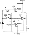
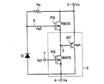
图1是表示本发明实施例1的半导体装置的等效电路的图。在图1中,半导体装置包含:PNP双极型晶体管(第1双极型晶体管)BT;控制该PNP双极型晶体管BT的基极电流的N沟道MOS晶体管(第1绝缘栅型场效应晶体管)NQ;在双极型晶体管BT断开时阻断载流子注入的P沟道MOS晶体管(第2绝缘栅型场效应晶体管)PQ。FIG. 1 is a diagram showing an equivalent circuit of a semiconductor device according to
双极型晶体管BT的发射极区域(第1导通节点)连接在集电极电极节点(第1电极节点)3上,其集电极区域(第2导通节点)连接在发射极电极节点(第2电极节点)4上。MOS晶体管NQ的源极耦合在发射极电极节点4上,在其栅极电极节点7上接受控制信号Vg1,其漏极连接在双极型晶体管BT的基极区5上。MOS晶体管NQ的背栅(基极)与源极相互连接。The emitter region (first conduction node) of the bipolar transistor BT is connected to the collector electrode node (first electrode node) 3, and the collector region (second conduction node) is connected to the emitter electrode node (the first conduction node). 2 electrode node) on 4. The source of the MOS transistor NQ is coupled to the
MOS晶体管PQ的源极区(第3导通节点)连接在集电极电极节点3,其基极(背栅)及漏极(第4导通节点)连接在双极型晶体管BT的基极节点(基极节点)5上。由双极型晶体管BT及MOS晶体管NQ构成的电路部分2对应于通常的IGBT的等效电路。在以下说明中提到IGBT时,就参照该方框2表示的部分。The source region (third conduction node) of the MOS transistor PQ is connected to the
图1所示的半导体装置还包含连接在MOS晶体管PQ的栅极电极节点6与发射极电极节点4之间的电压缓和元件1。在MOS晶体管PQ的非导通状态时,通过该电压缓和元件1缓和施加在栅绝缘膜上的电压。The semiconductor device shown in FIG. 1 further includes a
在本实施例1中,该电压缓和元件1由PN结二极管(二极管元件)Di构成。该PN结二极管Di的阴极连接在MOS晶体管PQ的栅极电极节点6上,阳极连接在发射极电极节点4上。In the first embodiment, the
现在考虑,如图2所示,在该半导体装置的集电极电极节点3上连接有电感性负载LL的情况。该电感性负载LL连接在供给高侧电压Vh的电源节点与集电极电极节点3之间。在MOS晶体管PQ的栅极电极节点6与集电极电极节点3之间存在栅电容Cg,另外,在二极管元件Di中,也存在由PN结产生的寄生电容Cd。Now consider a case where an inductive load LL is connected to the
在图2所示的结构中,IGBT2一旦接通,由于该电感性负载LL的L·(di/dt)成分,高侧电压Vh的大部分就施加在电感性负载LL上,集电极电极节点3的集电极电位Vc急剧下降。另一方面,在IGBT2断开时,集电极电极节点3的集电极电位Vc构成与高侧电压Vh大致相等的电平。此时,MOS晶体管PQ具有其阈值电压的绝对值(以下简称阈值电压)Vthp。另外,发射极电极节点4的发射极电位Ve通常设定在施加在半导体装置上的电压中的最低电位上。In the structure shown in Figure 2, once IGBT2 is turned on, due to the L·(di/dt) component of the inductive load LL, most of the high-side voltage Vh is applied to the inductive load LL, and the collector electrode node The collector potential Vc of 3 drops sharply. On the other hand, when the IGBT2 is turned off, the collector potential Vc of the
以下说明中,「导通状态」及「非导通状态」分别具有与「ON状态」及「OFF状态」相同的意思。特别在强调电流的有无时,使用「导通状态」及「非导通状态」的用语。In the following description, "conduction state" and "non-conduction state" have the same meanings as "ON state" and "OFF state", respectively. Especially when emphasizing the presence or absence of current, the terms "conduction state" and "non-conduction state" are used.
在IGBT2导通时施加在MOS晶体管NQ的栅极电极节点7上的控制电压Vg1被设定在H电平,MOS晶体管NQ成为导通状态。因此,向双极型晶体管BT供给基极电流,双极型晶体管BT成为导通状态,IGBT2接通。一旦IGBT2接通,随着集电极电极节点3的集电极电位Vc的下降,MOS晶体管PQ的栅极电极节点6的电位Vg2根据电容Cg及Cd的电容值而下降。一旦栅极电极节点6的栅电位Vg2达到发射极电极节点4的发射极电位Ve,由于二极管元件Di的正向偏置动作,栅极电极节点6的栅电位Vg2的电位下降就被抑制,栅电位Vg2的最低电位被二极管Di箝位。When IGBT2 is turned on, control voltage Vg1 applied to
在该IGBT2导通时集电极电极节点3的集电极电位Vc与栅极电极节点6的栅电位Vg2之差(Vc-Vg2)一旦成为MOS晶体管PQ的阈值电压Vthp以下(一旦成为Vc-Vg2<Vthp),MOS晶体管PQ就成为OFF状态。因而,在该接通动作中,不进行限制对于PNP双极型晶体管BT的空穴注入的限制动作。When the IGBT2 is turned on, the difference (Vc-Vg2) between the collector potential Vc of the
另一方面,在IGBT2断开动作时,向MOS晶体管NQ的栅极电极节点7施加的控制电压Vg1被设定在例如0V,MOS晶体管NQ成为OFF状态。因此,停止向双极型晶体管BT的基极电流的供给,PNP双极型晶体管BT向OFF状态转移。根据向该双极型晶体管BT的OFF状态的转移,集电极电极节点3的集电极电位Vc上升。另外,对应于集电极电位Vc上升,栅电位Vg2的电位也由于寄生电容Cg及Cd的作用而上升。On the other hand, when IGBT2 is turned off, control voltage Vg1 applied to
在该IGBT2断开时,集电极电位Vc与栅电位Vg2之差(Vc-Vg2)一旦成为比MOS晶体管PQ的阈值电压大,MOS晶体管PQ就成为ON状态,PNP双极型晶体管BT的发射极区域与基极区(基极节点5)被短路。从而,从集电极电极节点3注入的电流由MOS晶体管PQ排出,阻断向PNP双极型晶体管BT的空穴供给。When the IGBT2 is turned off, once the difference between the collector potential Vc and the gate potential Vg2 (Vc-Vg2) becomes larger than the threshold voltage of the MOS transistor PQ, the MOS transistor PQ becomes ON, and the emitter of the PNP bipolar transistor BT region is shorted to the base region (base node 5). Accordingly, the current injected from the
在该断开时,由于阻断了对PNP双极型晶体管BT的发射极区域的空穴供给,双极型晶体管BT的基极区的载流子排出一旦结束,集电极电极节点3的集电极电位Vc就高速上升。从而,可将尾电流流过的期间缩短,减少开时的开关损失,并实现高速动作。另外,在该IGBT2的ON状态(导通状态)时,双极型晶体管BT的集电极-发射极间电压Vce充分低,可以实现低ON电压。At this off time, since the supply of holes to the emitter region of the PNP bipolar transistor BT is blocked, once the discharge of carriers from the base region of the bipolar transistor BT is completed, the
在该断开过程等的过渡状态时,栅电位Vg2被设定在由二极管元件Di的寄生电容Cd和MOS晶体管PQ的栅电容Cg决定的电压电平上。该栅电位Vg2的电压电平是发射极电位Ve与集电极电位Vc之间的电压电平。In a transient state such as this off process, the gate potential Vg2 is set at a voltage level determined by the parasitic capacitance Cd of the diode element Di and the gate capacitance Cg of the MOS transistor PQ. The voltage level of the gate potential Vg2 is a voltage level between the emitter potential Ve and the collector potential Vc.
在成为断开状态、IGBT2处于OFF状态(非导通状态)的情况下,二极管Di是反向偏置状态。这时,由于二极管元件Di的漏电流等原因,栅电位Vg2最终成为与发射极电位Ve相同的电位。但是,如以下说明的那样,在实际器件结构中,由于该栅极电极节点6和集电极电极节点3之间流过的电流与在该栅电容Cg及二极管的结电容Cd上施加的电压平衡,栅电位Vg2平衡且大致稳定地维持在发射极电位Ve与集电极电位Vc之间的电压(例如穿通电压)上。When the diode Di is in the OFF state and the IGBT2 is in the OFF state (non-conductive state), the diode Di is in a reverse biased state. At this time, the gate potential Vg2 eventually becomes the same potential as the emitter potential Ve due to leakage current of the diode element Di or the like. However, as explained below, in an actual device structure, since the current flowing between the
因而,MOS晶体管PQ的栅极电极节点6的栅电位Vg2可设定在比发射极Ve高的电压电平上,可降低施加在MOS晶体管PQ的栅绝缘膜上的电压。从而能够减薄栅绝缘膜。另外,在非导通状态时,由于降低施加在栅绝缘膜上的电压,无需为保障与其它周边区域之间的耐压而设置相对于周边区域(电极层等)的充分距离,可以减少元件(单元)的占有面积。Therefore, the gate potential Vg2 of the
图3是概略表示本发明实施例1的半导体装置的剖面结构的图。在图3中,半导体装置形成在P型半导体衬底(半导体衬底区)10上。在该P型半导体衬底区10的表面上间隔地设置N型半导体区(第1及第2半导体区)12a及12b。3 is a diagram schematically showing a cross-sectional structure of a semiconductor device according to
设置P型半导体区(第3半导体区)13,以包围该N型半导体区12a的一部分(下区域)。这里,在该半导体装置中,没有示出平面布局,但将示于图3的右侧的LI为中心,同心圆状地形成各区域。因此,就P型半导体区13形成为包围N型半导体区12a的情况进行说明。P型半导体区13具有在IGBT断开时将空穴向发射极电极节点排出的功能。A P-type semiconductor region (third semiconductor region) 13 is provided so as to surround a part (lower region) of this N-
在该P型半导体区13上及N型半导体区12a的一部分表面上,设置P型半导体区(第4半导体区)14,在该P型半导体区14内部,设置高浓度的N型杂质区(第1杂质区)15。P型半导体区14形成为包围N型杂质区,设置构成连接在发射极电极节点4的发射极的电极层(第1电极层)16,连接在P型半导体区14及N型杂质区15这二者上。该发射极电极层16将图1所示的N沟道MOS晶体管NQ的背栅与源极相互连接,并电连接至发射极电极节点4。On the P-
在P型半导体区14表面上,隔着栅绝缘膜(第1绝缘膜)17而形成构成连接在栅极电极节点7上的栅电极的电极层(第2电极层)18。该栅绝缘膜17及栅极电极层18延伸而形成到N型半导体区12a上,根据控制电压Vg 1,在N型杂质区15与N型半导体区12a之间的P型半导体区14表面上形成沟道。An electrode layer (second electrode layer) 18 constituting a gate electrode connected to the
在N型半导体区12a表面上,离开P型半导体区14且相互分离地形成P型杂质区(第2及第3杂质区)19a及19b。在这些P型杂质区19a及19b之间的N型半导体区12a上,隔着栅绝缘膜(第2绝缘膜)20而形成构成栅极电极节点6的电极层(第4电极层)21。另外,与P型杂质区19b邻接地形成N型杂质区(第4杂质区)22。在P型杂质区19a表面上,形成构成连接在图1所示的集电极电极节点3上的集电极的电极层(第3电极层)23。另外,在杂质区19b及22这二者的表面上,形成构成图1所示的基极节点5电极层(第4电极层)24。On the surface of the N-
在N型半导体区12b表面上,形成N型杂质区(第5杂质区)25。在该N型杂质区25表面上,形成电连接至栅极电极层21的电极层(第5电极层)26。该电极层26对应于图1所示的二极管元件Di的阴极。在二极管元件Di的非导通状态时,使其在N型半导体区12a及12b之间的P型半导体区10上产生穿通(使其在PN结上产生穿通击穿),用该穿通电压来限制施加在栅极电极层21上的电压。On the surface of the N-
即,如果该N型杂质区22与P型半导体衬底区10之间的电压达到穿通电压,则耗尽层从N型杂质区22到达半导体衬底区10,在P型半导体衬底区10表面的PN结上产生穿通击穿。另外,如果耗尽层从N型杂质区25延伸,耗尽层一旦到达半导体衬底区10,在该N型半导体区12b与半导体衬底区10之间的PN结上就产生穿通击穿。由于该穿通击穿,在P型半导体衬底区10表面上,N型半导体区12a及12b之间通过耗尽层而导通,来自N型杂质区22的电压通过N型杂质区25及电极层26传递至栅极电极层21,可以抑制栅电位Vg2的降低。如果栅电位Vg2上升,则P沟道MOS晶体管的沟道电阻变大,N型杂质区22的电压电平变低,半导体衬底区10表面的PN结的穿通击穿消失,栅电位Vg2的上升停止。从而,栅极电极层21的电压电平比发射极电极层16的发射极电位Ve高,维持在由穿通电压决定的电压电平上。That is, if the voltage between the N-
在图3所示的结构中,N沟道MOS晶体管NQ基本上由P型半导体区14、N型杂质区15、栅绝缘膜17、电极层18及N型半导体区(漂移层)12a构成。N沟道MOS晶体管NQ的背栅由P型半导体区14形成,该背栅和源极(杂质区15)通过电极层16电连接。In the structure shown in FIG. 3, the N-channel MOS transistor NQ is basically composed of a P-
P沟道MOS晶体管PQ基本上由P型杂质区19a及19b、N型半导体区12a、栅绝缘膜20、电极层21构成。构成P沟道MOS晶体管PQ的背栅的N型半导体区12a通过N型杂质区22耦合到电极层24。从而,在被电连接到基极节点5电极层24上,可以实现P沟道MOS晶体管PQ的背栅与漏极相互连接的结构。P-channel MOS transistor PQ is basically composed of P-
二极管Di基本上用N型杂质区25、N型半导体区12b、P型半导体衬底区10以及P型半导体区13和14构成。利用N型半导体区12b和P型半导体衬底区10之间的PN结的电容,通过电容分隔来使栅极电极节点6的电位Vg2在IGBT断开时降低。The diode Di is basically composed of the N-
PNP双极型晶体管BT基本上由P型杂质区19a、N型半导体区12a、P型半导体区13及14来形成,该N型半导体区12a作为双极型晶体管的基极区起作用。The PNP bipolar transistor BT is basically formed of a P-
在图3所示的结构中,在IGBT的导通时施加在电极层18上的控制电压Vg 1被设定在正电压电平上,在N型杂质区15与N型半导体区12a之间的P型半导体区14表面上形成沟道,电子从发射极电极层16向N型半导体区12a流动。并且,这时从集电极电极层23经由P型杂质区19a向N型半导体区12a流入空穴。因此,在N型半导体区12a中产生电导率调制,其电阻值下降,更多的电流流过该N型半导体区12a。因此,双极型晶体管BT的基极电流变大,双极型晶体管(BT)成为ON状态。在该导通时即使集电极电极层23的电位降低,P型杂质区19a与栅极电极层21之间的电位差也是在P沟道MOS晶体管的阈值电压Vthp以下,P沟道MOS晶体管被维持在OFF状态。因而,对从集电极电极层23向N型半导体区12a的空穴供给不带来任何不良影响。In the structure shown in FIG. 3, the control voltage Vg1 applied to the
在该导通时杂质区19a、19b及22是N型半导体区12a的电位电平,大体上是发射极电位Ve的电平,另外,半导体衬底区10是发射极电位Ve的电平。在二极管元件Di中,N型半导体区12b及半导体衬底区10之间的PN结是反向偏置,被维持在OFF状态。The
在IGBT断开时,对于栅极电极层18的控制电压Vg 1被设定在例如0V上,P型半导体区14表面的沟道(反转层)消失。从而,向N型半导体区12a的电流路径被阻断,双极型晶体管BT向断开状态转移。一旦集电极电极层23的电压Vc上升,该P型杂质区19a与栅极电极层21之间的电位差变得比P沟道MOS晶体管的阈值电压Vthp大,P沟道MOS晶体管成为ON状态。在P型杂质区19a和19b之间的N型半导体区12a表面上形成沟道,从集电极电极层23供给的空穴和残存于N型半导体区12a的载流子(空穴)由P型杂质区19b吸收,向N型半导体区12a的空穴供给被阻断。When the IGBT is turned off, the control voltage Vg1 to the
半导体区12a中的残存载流子(空穴)通过发射极电极层16的排出一旦结束,双极型晶体管就成为OFF状态,IGBT成为OFF状态。在该OFF状态,N型半导体衬底区12a与P型半导体衬底区10之间的PN结成为反向偏置状态,耗尽层从P型半导体衬底区10向N型半导体区12a扩展,耗尽层最终达到N型半导体区12a的表面。从而,缓和了N型半导体区12a表面的电场集中,实现了高耐压结构。Once the remaining carriers (holes) in the
另外,在该IGBT断开时,栅极电极层21上的栅电位Vg2随着集电极电位Vc的上升,其电压电平通过栅电容的电容耦合而上升。这时,通过由N型半导体区12b与半导体衬底区10之间的PN结电容产生的电容耦合,抑制栅电位Vg2的上升。电压差Vc-Vg2一旦成为阈值电压Vthp以下,在栅极电极层21下部就形成沟道,P型杂质区19a、19b与N型半导体区12a通过沟道而成为同一电位,来自N型半导体区12a的向集电极电极层23的空穴供给被阻断。Also, when the IGBT is turned off, the gate potential Vg2 on the
集电极电位Vc通过P型杂质区19b、基极电极层24及N型杂质22传达。因此,N型半导体区12a与半导体区10之间的PN结成为反向偏置状态,在N型半导体区12a及12b之间的PN结上产生穿通击穿,N型半导体区12a及12b之间成为穿通状态。因此,可通过该穿通电压抑制控制电压Vg2的电压电平的下降,用该电压电平维持栅电位Vg2的电位电平。The collector potential Vc is transmitted through the P-
栅极电极层21上的栅电位Vg2是发射极电位(Ve)与集电极电位(Vc)之间的电位电平。因而,施加在栅绝缘膜20上的电压,即集电极电极层23的电压与栅极电极层21上的控制电压Vg2之差成为比集电极-发射极间电压小。因而,可以减薄栅绝缘膜20的膜厚。另外,可以缓和施加在该栅绝缘膜20上的电压,无需设置拉开该集电极电极层23与栅极电极层21之间的距离,或加大栅极电极层21与基极电极层24之间的距离以及栅极电极层21与集电极电极层23之间的距离等用以确保耐压的结构,因此,可以减少该半导体装置的整体布局面积。The gate potential Vg2 on the
另外,在根据集电极电极层23的集电极电压,在N型半导体区12a和12b之间产生穿通时,控制电压Vg2的电压电平的降低就受到该穿通电压抑制。因而,该N型半导体区12a和12b之间的距离设定在可使穿通产生的范围。Also, when a punchthrough occurs between the N-
如上所述,依据本发明的实施例1,将二极管元件作为电压缓和元件连接在用以减少断开损失的P沟道MOS晶体管的栅极电极节点与发射极电极节点之间。从而,不会对P沟道MOS晶体管的ON及OFF动作带来不良影响,可以缓和该P沟道MOS晶体管在断开时施加在栅绝缘膜上的电压。从而,可以实现占用面积小且具有高耐压结构及低损失的半导体装置。As described above, according to
[实施例2][Example 2]
图4是表示本发明实施例2的半导体装置的等效电路的图。图4所示的半导体装置与图1所示的实施例1的半导体装置在结构上的不同点是,在双极型晶体管BT的基极节点5与MOS晶体管PQ的栅极电极节点6之间逆向连接齐纳二极管ZDi。该齐纳二极管ZDi的阳极连接在二极管元件Di的阴极及MOS晶体管PQ的栅电极上,其阴极连接在基极节点5上。4 is a diagram showing an equivalent circuit of a semiconductor device according to
齐纳二极管ZDi是恒压二极管,在施加反向偏置电压时导通,在其基极节点5与栅极电极节点6之间使其产生一定大小的电压(齐纳电压)。The Zener diode ZDi is a constant voltage diode, which is turned on when a reverse bias voltage is applied, and generates a certain voltage (Zener voltage) between the
图4所示的半导体装置的其它结构与图1所示的半导体装置的结构相同,在对应的部分上附加相同的附图标记,省略其详细说明。Other configurations of the semiconductor device shown in FIG. 4 are the same as those of the semiconductor device shown in FIG. 1 , and corresponding parts are assigned the same reference numerals, and detailed description thereof will be omitted.
图5是概略表示图4所示的半导体装置的剖面结构的图。图5所示的结构与图3所示的半导体装置的剖面结构不同。即,在N型半导体区(第1半导体区)12a中,在N型杂质区(第4杂质区)22的近旁形成P型杂质区(第7杂质区)28,连接在该P型杂质区28底部而设置高浓度N型杂质区(第6杂质区)29。P型杂质区28经由电极层30连接至栅极电极层21及阴电极层26。该P型杂质区28对应于齐纳二极管ZDi的阳极,N型杂质区29相当于齐纳二极管ZDi的阴极。通过该杂质区28及29,可在N型半导体区12a内以简单的结构设置齐纳二级管,无需在外部另设齐纳二级管。FIG. 5 is a diagram schematically showing a cross-sectional structure of the semiconductor device shown in FIG. 4 . The structure shown in FIG. 5 is different from the cross-sectional structure of the semiconductor device shown in FIG. 3 . That is, in the N-type semiconductor region (first semiconductor region) 12a, a P-type impurity region (seventh impurity region) 28 is formed near the N-type impurity region (fourth impurity region) 22, and is connected to the P-type impurity region. 28 and a high-concentration N-type impurity region (sixth impurity region) 29 is provided. The P-
该图5所示的半导体装置的其它结构与图3所示的半导体装置的结构相同,在对应的部分上附带相同的附图标记,省略其详细说明。Other configurations of the semiconductor device shown in FIG. 5 are the same as those of the semiconductor device shown in FIG. 3 , and corresponding parts are assigned the same reference numerals, and detailed description thereof will be omitted.
如实施例1中说明过的那样,在IGBT2的OFF状态时,在形成二极管元件Di的阴极的N型半导体区12b与构成P沟道MOS晶体管的背栅的N型半导体区10之间产生穿通,以抑制栅电压Vg2的电位电平的下降。为了增强IGBT断开时的P沟道MOS晶体管的动作,即为了增强抑制空穴向基极区(半导体区12a)流入的动作,栅电位Vg2以低者为好。但是,如果该栅电位Vg2变得过低,则有产生以下问题的可能性。即,集电极电极层23的集电极电位Vc一旦上升,P型杂质区19a与栅极电极层21之间的电位差就变大,施加在栅绝缘膜20上的电压会变得过高,存在使耐压特性受损的可能性。另外,在N型半导体区12a及12b的相对电位差大的情况下,不能保障PN结的耐压,有IGBT的耐压降低的可能性。As described in
为了回避上述问题,设置齐纳二极管ZDi。即,在栅电位Vg2降低,集电极电位Vc上升,基极节点5与栅极电极节点6之间的电位差变大的情况下,由于齐纳二极管ZDi的齐纳击穿,从而抑制该栅电位Vg2的电压降低。In order to avoid the above problems, a Zener diode ZDi is provided. That is, when the gate potential Vg2 falls, the collector potential Vc rises, and the potential difference between the
即,如图5所示,基极节点5经由电极层24及N型杂质区22连接到P沟道MOS晶体管的背栅即双极型晶体管的基极区上,并经由P型杂质区19a电连接至集电极电极层23(集电极电极节点3)。因而,该栅电位Vg2降低时,反向偏置电压施加在杂质区29及28之间,使得在P型杂质区28和N型杂质区29之间的PN结上产生齐纳击穿。通过产生该齐纳击穿的PN结,从N型半导体区12a向栅极电极层21(栅极电极节点6)供给电流,使栅电位Vg2的电位电平上升。即,该栅电位Vg2的电位被箝位在比集电极电位Vc大约低齐纳电压的电压电平上。从而,抑制在IGBT断开时P沟道MOS晶体管的栅绝缘膜20上被施加高电压,另外,防止N型半导体区12a及12b之间的电位差变得过大,抑制IGBT耐压的降低。That is, as shown in FIG. 5, the
由二极管元件Di产生的电压缓和动作与实施例1的相同。The voltage relaxation operation by the diode element Di is the same as that of the first embodiment.
如上所述,依据本发明的实施例2,在双极型晶体管的基极节点与P沟道MOS晶体管的栅极电极节点之间连接恒压二极管(齐纳二极管)。从而,在实施例1的效果之外,还可得到以下的效果。即,可以抑制断开时集电极电位与P沟道MOS晶体管的栅电位之差变大,能够可确保P沟道MOS晶体管的绝缘耐压,另外,可以抑制由于穿通电压产生的IGBT自身的耐压特性的劣化。As described above, according to
[实施例3][Example 3]
图6是表示本发明实施例3的半导体装置的等效电路的图。图6所示的半导体装置与按照图4在如下这点上与所示的实施例2的半导体装置的结构不同。即,齐纳二极管(恒压二极管)ZDi连接在集电极电极节点3与P沟道MOS晶体管的栅极电极节点6之间。该图6所示的半导体装置的其它结构与图4所示的半导体装置的结构相同,在对应的部分上附加相同的附图标记,省略其详细说明。6 is a diagram showing an equivalent circuit of a semiconductor device according to
该齐纳二极管ZDi的阳极连接在MOS晶体管PQ的栅极电极节点6以和二极管元件Di的阴极上,其阴极连接在集电极电极节点3上。The anode of Zener diode ZDi is connected to
在图6所示的半导体装置中,集电极电极节点3的集电极电位Vc与栅极电极节点6的栅电位Vg2的电位差一变大,齐纳二极管ZDi就导通,将该栅电位Vg2箝位在比集电极电位Vc低齐纳击穿电压的电压电平上。因而,在图6所示的半导体装置中,也可通过与实施例2同样的动作,得到同样的效果。In the semiconductor device shown in FIG. 6, when the potential difference between the collector potential Vc of the
[实施例4][Example 4]
图7是表示本发明实施例4的半导体装置的等效电路的图。该图7所示的半导体装置的结构在如下这点上与图1所示的半导体装置的结构不同。即,在双极型晶体管BT的基极节点5与二极管元件Di的阴极之间,连接PNP双极型晶体管(第2双极型晶体管)BBD。该PNP双极型晶体管BBD的基极及发射极相互连接,并连接在基极节点5上,其集电极连接在二极管元件Di的阴极及P沟道MOS晶体管PQ的栅极电极节点6上。该双极型晶体管BBD的基极及发射极相互连接,等效地作为将集电极作为阳极,将基极和发射极作为阴极的二极管起作用。该栅电位Vg2降低时,由于反向偏置电压,使其在集电极-发射极间产生穿通,抑制栅电位Vg2的降低。7 is a diagram showing an equivalent circuit of a semiconductor device according to
该图7所示的半导体装置的其它结构与图1所示的半导体装置的结构相同,在对应的部分上附加相同附图标记,省略其详细说明。Other configurations of the semiconductor device shown in FIG. 7 are the same as those of the semiconductor device shown in FIG. 1 , and corresponding parts are assigned the same reference numerals, and detailed description thereof will be omitted.
图8是概略表示图7所示的半导体装置的剖面结构的图。图8所示的半导体装置的剖面结构在如下这点上与图3所示的半导体装置的剖面结构不同。即,P型杂质区(第6杂质区)32邻接于构成PNP双极型晶体管BT的基极的N型杂质区(第4杂质区)22而形成在N型半导体区(第1半导体区)12a表面上,另外,在N型半导体区12a表面上与该P型杂质区32间隔地形成P型杂质区(第7杂质区)34。构成PNP双极型晶体管BT的基极节点5电极层(第5电极层)35电连接在P型杂质区19、N型杂质区22及P型杂质区32上。P型杂质区34通过电极层36电连接在构成P沟道MOS晶体管的栅极电极节点6的电极层(第4电极层)21上。FIG. 8 is a diagram schematically showing a cross-sectional structure of the semiconductor device shown in FIG. 7 . The cross-sectional structure of the semiconductor device shown in FIG. 8 differs from the cross-sectional structure of the semiconductor device shown in FIG. 3 in the following point. That is, the P-type impurity region (sixth impurity region) 32 is formed in the N-type semiconductor region (first semiconductor region) adjacent to the N-type impurity region (fourth impurity region) 22 constituting the base of the PNP bipolar transistor BT. On the surface of the N-
该图8所示的半导体装置的剖面结构的其它结构与图3所示的半导体装置的剖面结构相同,在对应的部分上附加相同附图标记,省略其详细说明。The rest of the cross-sectional structure of the semiconductor device shown in FIG. 8 is the same as the cross-sectional structure of the semiconductor device shown in FIG. 3 , and corresponding parts are assigned the same reference numerals, and detailed description thereof will be omitted.
在图8所示的半导体装置中,用P型杂质区32、N型半导体区12a、N型杂质区22和P型杂质区34形成PNP双极型晶体管BBD。即,双极型晶体管BBD的基极由N型半导体区12a和N型杂质区22构成,发射极由P型杂质区32构成,集电极由P型杂质区34构成。双极型晶体管BBD的基极和发射极由电极层35相互连接。通过在N型半导体区12a表面上相互分离配置P型杂质区32及34,能够以简单的结构制作双极型晶体管BBD,可容易地将双极型晶体管BBD内设。In the semiconductor device shown in FIG. 8 , PNP bipolar transistor BBD is formed by P-
IGBT2断开时,集电极电位Vc上升。这时,由于二极管元件Di的作用,栅电位Vg2降低,MOS晶体管PQ成为导通状态。因此,杂质区22及32的电位随着集电极电压Vc而变高。这时,如果栅电位Vg2过低,基极节点5与栅极电极节点6之间的电位差成为穿通电压以上,则在P型杂质区32及34之间形成耗尽层,在P型杂质区34与半导体区12a之间的PN结上产生穿通击穿,根据经由导通状态的PMOS晶体管PQ施加的电压,栅电位Vg2的电压电平降低得到抑制。When IGBT2 is turned off, the collector potential Vc rises. At this time, the gate potential Vg2 is lowered by the action of the diode element Di, and the MOS transistor PQ is turned on. Therefore, the potentials of the
这时,双极型晶体管BBD与前面实施例3的齐纳二极管ZDi同样动作,箝位该栅电位Vg2的电压电平。这时,在栅极电极节点6的栅电位Vg2过低的情况下,P型杂质区34及32之间的耗尽层被连接,在杂质区34与N型半导体区12a之间的PN结上产生穿通击穿,该双极型晶体管BBD的基极/发射极与集电极之间导通,抑制栅电位Vg2的电位降低。这时,利用了双极型晶体管BBD的穿通现象,即利用了PN结的穿通击穿。这时,穿通电压可由杂质浓度和杂质区32及34之间的距离进行调整。另外,与使用二极管的情况相比,可以将穿通电压设定在比使雪崩击穿发生的电压电平高的电压电平上,可将栅电位Vg2的电位电平设定在比利用雪崩击穿时低的电压电平上。At this time, the bipolar transistor BBD operates similarly to the Zener diode ZDi of the third embodiment, and clamps the voltage level of the gate potential Vg2. At this time, when the gate potential Vg2 of the
再者,在图7中,使用PNP双极型晶体管BBD。但是,为了得到该穿通特性,也可以使用NPN双极型晶体管。在使用NPN双极型晶体管时,其基极和集电极连接在栅极电极节点6上,其发射极连接在基极节点5上。从而,可以利用PN结的穿通现象抑制栅电位Vg2的电压电平的降低。In addition, in FIG. 7, the PNP bipolar transistor BBD is used. However, in order to obtain this punch-through characteristic, an NPN bipolar transistor may also be used. When using an NPN bipolar transistor, its base and collector are connected to the
如上所述,按照本发明的实施例4,在IGBT的双极型晶体管的基极节点与P沟道MOS晶体管的栅极电极节点之间连接被接成二极管的双极型晶体管。因而,可以在实施例1的效果之外取得以下的效果。即,可以防止P沟道MOS晶体管的栅电位的过多降低,可以保障P沟道MOS晶体管的栅绝缘膜的耐压。另外,与利用雪崩击穿或齐纳击穿的情况相比,利用PN结的穿通现象时,可以用P型杂质区的杂质浓度和半导体区的杂质浓度以及发射极杂质区-集电极杂质区之间的距离进行调整,可以正确地调整穿通电压,另外,可以将P沟道MOS晶体管的栅电位设定在低的电位电平上,在IGBT断开时能够使P沟道MOS晶体管高速转移至ON状态。As described above, according to
再者,二极管元件Di的动作及效果与实施例1的情况相同。In addition, the operation and effect of the diode element Di are the same as those of the first embodiment.
[实施例5][Example 5]
图9是表示本发明实施例5的半导体装置的等效电路的图。图9所示的半导体装置在如下这点上与图7所示的半导体装置其电路结构不同。即,被接成二极管的PNP双极型晶体管(第2双极型晶体管)BBD2不在连接基极节点5和栅极电极节点6之间,而是连接在集电极电极节点(第1电极节点)3与栅极电极节点6之间。该PNP双极型晶体管BBD2的基极和发射极连接在集电极电极节点3上,集电极连接在栅极电极节点6上。9 is a diagram showing an equivalent circuit of a semiconductor device according to
图9所示的半导体装置的其它结构与图7所示的半导体装置的结构相同,在对应的部分上附加相同附图标记,省略其详细说明。Other configurations of the semiconductor device shown in FIG. 9 are the same as those of the semiconductor device shown in FIG. 7 , and corresponding parts are assigned the same reference numerals, and detailed description thereof will be omitted.
在图9所示的半导体装置的结构中,集电极电极节点3的集电极电位Vc与栅极电极节点6的栅电位Vg2的电压差一变大,双极型晶体管BBD2就会由于反向偏置而引起穿通现象,该穿通电压抑制栅电位Vg2的降低。从而,可以抑制P沟道MOS晶体管PQ的栅电位Vg2的降低,可得到与实施例4同样的效果。该PNP双极型晶体管BBD2的动作细节与实施例4的情况相同。即,基极/集电极间的PN结由于反向偏置电压而产生穿通击穿,从集电极电极节点3向栅极电极节点6供给电流。在该状态,集电极电极节点3与栅极电极节点6之间的电压成为穿通电压电平。In the structure of the semiconductor device shown in FIG. 9 , when the voltage difference between the collector potential Vc at the
二极管元件Di的作用及效果与实施例1的情况相同。The action and effect of the diode element Di are the same as those of the first embodiment.
[变更例][change example]
图10是表示本发明实施例5的半导体装置的变更例的等效电路的图。该图10所示的半导体装置在如下这点上与图9所示的半导体装置的电路结构不同。即,用NPN双极型晶体管(第2双极型晶体管)BBD3取代了PNP双极型晶体管BBD2。该NPN双极型晶体管BBD3的基极和集电极连接在栅极电极节点6,其发射极连接在集电极电极节点3上。10 is a diagram showing an equivalent circuit of a modified example of the semiconductor device according to
图10所示的半导体装置的其它结构与图9所示的半导体装置的结构相同,在对应的部分上附加相同附图标记,省略其详细说明。Other configurations of the semiconductor device shown in FIG. 10 are the same as those of the semiconductor device shown in FIG. 9 , and corresponding parts are assigned the same reference numerals, and detailed description thereof will be omitted.
在图10所示的半导体装置中,也利用由NPN双极型晶体管BBD3的基极-发射极间的反向偏置电压产生的穿通现象(PN结的穿通击穿)来抑制栅电位Vg2的降低。因而,可以得到与图9所示的半导体装置的结构同样的效果。Also in the semiconductor device shown in FIG. 10, the punch-through phenomenon (puncture breakdown of the PN junction) caused by the reverse bias voltage between the base and the emitter of the NPN bipolar transistor BBD3 is used to suppress the variation of the gate potential Vg2. reduce. Therefore, the same effect as that of the structure of the semiconductor device shown in FIG. 9 can be obtained.
如上所述,按照本发明的实施例5,在集电极电极节点与P沟道MOS晶体管的栅极电极节点之间连接被接成二极管的双极型晶体管,以利用其穿通现象。从而,可以使其产生较高电压的穿通现象,另外,可以正确地设定穿通电压,更可靠进行其栅极电极节点的电位控制。另外,与实施例1一样,可以在维持P沟道MOS晶体管的ON/OFF特性的同时维持栅绝缘膜的耐压特性。并且,可取得与实施例1同样的效果。As described above, according to
[实施例6][Example 6]
图11是表示本发明实施例6的半导体装置的等效电路的图。在图11所示的半导体装置中,作为电压缓和元件1,使用P沟道结型场效应晶体管(JFET)JQ1。该结型场效应晶体管JQ1的栅极连接在基极节点5上,漏极及源极区分别连接在发射极电极节点4及栅极电极节点6上。在结型场效应晶体管JFET中,由于源极区及漏极区对称形成,在图11中,结型场效应晶体管JQ1的源极及漏极可为任一节点,将连接在电位高的栅极电极节点6上的节点作为源极电极节点,将连接在发射极电极节点4上的节点作为漏极电极节点,如此进行以下的说明。11 is a diagram showing an equivalent circuit of a semiconductor device according to
图11所示的半导体装置的其它结构与图1所示的半导体装置的结构相同,在对应的部分上附加相同的附图标记,省略其详细说明。Other configurations of the semiconductor device shown in FIG. 11 are the same as those of the semiconductor device shown in FIG. 1 , and corresponding parts are assigned the same reference numerals, and detailed description thereof will be omitted.
图12是概略表示图11所示的半导体装置的剖面结构的图。图12所示的半导体装置的剖面结构在如下这点上与图3所示的半导体装置的剖面结构不同。即,与N型半导体区(第1半导体区)12a相隔离地在半导体衬底区10的表面上形成N型半导体区(第2半导体区)12c。从N型半导体区12a的一部分区域直到N型半导体区12c的一部分区域,连续地形成P型杂质区(第5杂质区)40。该P型杂质区40经由在其表面上形成的电极层42电连接到栅极电极层(第4电极层)21上。FIG. 12 is a diagram schematically showing a cross-sectional structure of the semiconductor device shown in FIG. 11 . The cross-sectional structure of the semiconductor device shown in FIG. 12 is different from the cross-sectional structure of the semiconductor device shown in FIG. 3 in the following point. That is, an N-type semiconductor region (second semiconductor region) 12c is formed on the surface of the
图12所示的半导体装置的剖面结构的其它结构与图3所示的半导体装置的剖面结构相同,在对应的部分上附加相同附图标记,省略其详细说明。The rest of the cross-sectional structure of the semiconductor device shown in FIG. 12 is the same as the cross-sectional structure of the semiconductor device shown in FIG. 3 , and corresponding parts are assigned the same reference numerals, and detailed description thereof will be omitted.
在图12所示的剖面结构中,N型杂质区22作为P沟道结型场效应晶体管JQ1的栅电极起作用,P型杂质区40下部的N型半导体区12a及12c之间的P型半导体衬底区10作为该P沟道结型场效应晶体管的沟道区被利用。P型杂质区40作为源极被利用。N型半导体区12a及12c分离而配置,在其间的半导体衬底区10的表面上配置P型杂质区40,从而能够以简单的结构实现内置结型场效应晶体管。In the cross-sectional structure shown in FIG. 12 , the N-
在IGBT断开时,集电极电极层23的集电极电位Vc上升。随着该集电极电位Vc上升,由于栅电容的作用,栅电位Vg2的电位上升。该栅极电极层21通过源极P型杂质区40耦合到P型半导体衬底区10,抑制其电位电平的上升。因此,P沟道MOS晶体管PQ成为ON状态,将P型杂质区19a及N型半导体区12a设定在同一电压电平上,从集电极电极节点23向N型半导体区12a的空穴供给被阻断。从而,PNP双极型晶体管BT高速断开。When the IGBT is turned off, the collector potential Vc of the
随着该集电极电位Vc的上升,N型半导体区12a的电位也上升,半导体区12a及半导体衬底区10之间的PN结被反向偏置,耗尽层在N型半导体区12a及12c之间的半导体衬底区10中扩展。这时,半导体区12a及12c之间的半导体衬底区10在完全耗尽化之前,P型杂质区40经由P型半导体区10及14而连接至发射极电极节点4上,栅电位Vg2被维持在发射极电位Ve的电位电平上。在此期间,PMOS晶体管PQ被维持在ON状态,来自集电极电极节点3的从双极型晶体管的发射极向基极的空穴供给被阻断。As the collector potential Vc rises, the potential of the N-
随着该集电极电位Vc的电位上升,耗尽层在半导体衬底区10中扩展,P型杂质区40下部的P型半导体衬底区10一旦完全耗尽,P型杂质区40就与P型半导体衬底区10电上隔离。因而,这时栅极电极层21的电位Vg2随着集电极电位Vc的电位上升而开始上升。该栅电位Vg2上升至由MOS晶体管PQ的栅电容与结型场效应晶体管JQ1的耗尽层电容所决定的电压电平。As the potential of the collector potential Vc rises, the depletion layer expands in the
调整该结型场效应晶体管的穿通电压,使结型场效应晶体管JQ1的沟道耗尽在P沟道MOS晶体管PQ接通后产生。穿通电压,即耗尽层的扩展可以用半导体区12a和12c之间的距离及杂质浓度和P型半导体衬底区10的杂质浓度的调整进行调整。The breakthrough voltage of the junction field effect transistor is adjusted so that the channel depletion of the junction field effect transistor JQ1 occurs after the P-channel MOS transistor PQ is turned on. The punch-through voltage, that is, the expansion of the depletion layer can be adjusted by adjusting the distance and impurity concentration between the
从而,在IGBT2断开的同时P沟道MOS晶体管PQ接通,且在该断开后使栅电位Vg2上升,可抑制在P沟道MOS晶体管PQ的栅绝缘膜20上被施加高电压(集电极-发射极间电压Vce)。Therefore, the P-channel MOS transistor PQ is turned on at the same time as the IGBT2 is turned off, and the gate potential Vg2 is raised after the turn-off, thereby suppressing the application of a high voltage (collector voltage) to the
[变更例][change example]
图13是概略表示本发明实施例6的半导体装置的变更例的剖面结构的图。该图13所示的半导体装置在如下这点上与图12所示的半导体装置结构不同。即,在P型半导体衬底区10的表面上相互间隔配置N型半导体区(第1及第2半导体区)12a及12e。在这些N型半导体区12a及12e之间,形成低浓度的P型半导体区(第5半导体区)48。在P型半导体区48的表面上,形成P型杂质区(第5杂质区)50,由该半导体区48包围。该P型杂质区50经由电极层52电连接至栅极电极层(第4电极层)21。13 is a diagram schematically showing a cross-sectional structure of a modified example of the semiconductor device according to
在N型半导体区12a及12e与P型半导体衬底区10之间,相互间隔地形成N型埋入杂质区(第1及第2埋入半导体区)44及46。这些N型埋入杂质区44及46的杂质浓度与N型半导体区12a及12e的杂质浓度以及P型半导体区48的杂质浓度相比,具有充分高的杂质浓度。这些N型埋入杂质区44及46之间的距离比半导体区12a及12e之间的距离短。Between the N-
P型半导体区48与P型半导体衬底区10通过N型埋入杂质区44及46之间的区域连通。P型半导体区48和N型半导体区44及46之间的半导体衬底区10,作为结型场效应晶体管JQ1的沟道区使用。P型杂质区48作为源极区使用,N型杂质区22、N型半导体区12a及12e以及N型埋入杂质区44及46作为栅极使用。在图13所示的结构中,也能够以简单的结构内置结型场效应晶体管。The P-
图13所示的半导体装置的其它结构与图12所示的半导体装置的结构相同,在对应的部分上附加相同附图标记,省略其详细说明。Other configurations of the semiconductor device shown in FIG. 13 are the same as those of the semiconductor device shown in FIG. 12 , and corresponding parts are assigned the same reference numerals, and detailed description thereof will be omitted.
在图13所示的半导体装置的情况下,当IGBT断开时,随着集电极电位Vc的电位上升,在P型半导体区48中,耗尽层从N型半导体区12a及N型埋入杂质区44扩展。这时,PN结是反向偏置状态,耗尽层从高浓度的N型埋入杂质区44向杂质浓度低的区域即P型半导体区48及半导体衬底区10快速扩展。在该耗尽层成为穿通状态之前,栅极电极层21通过电极层52、P型杂质区50、半导体区48以及半导体衬底区10耦合到发射极电极层18上,栅电位Vg2的上升被抑制。In the case of the semiconductor device shown in FIG. 13, when the IGBT is turned off, as the potential of the collector potential Vc rises, in the P-
随着集电极电位Vc的上升,耗尽层在N型埋入杂质区44及46之间的P型半导体区48中扩展,一旦耗尽层在高浓度N型埋入杂质区44及46之间穿通,结型场效应晶体管JQ就成为夹断状态,栅极电极层21与发射极电极层18被电隔离。在该耗尽层穿通状态下,耗尽层形成在高浓度的N型埋入杂质区44及46周边,耗尽层不能到达P型杂质区50,P型杂质区50处于由耗尽层包围的状态。电压施加在耗尽层上。因而,在夹断状态下,耗尽层端(夹断点)与P型杂质区50之间的电场不发生变化,可以将P型杂质区50的电压大致维持恒定。从而,P沟道结型场效应晶体管JQ1成为夹断状态后,可以将栅电位Vg2维持在大致恒定的电位电平上,可以将施加在栅绝缘膜20上的电压大致维持恒定。从而,能够以简单的结构可确保栅绝缘膜20的耐压。As the collector potential Vc rises, the depletion layer expands in the P-
如上所述,依据本发明的实施例6,作为电压缓和元件,利用P沟道结型场效应晶体管,利用由于该沟道区的耗尽层的扩展而使夹断产生的现象。因而,能够可靠地使P沟道MOS晶体管在IGBT断开时,一旦设定在ON状态后,就高速转换至OFF状态。另外,可以缓和施加在栅绝缘膜上的电压,与实施例1一样,可以在维持耐压特性的同时减少半导体装置(单元)的占有面积。As described above, according to
[实施例7][Example 7]
图14是表示本发明实施例7的半导体装置的等效电路的图。该图14所示的半导体装置在如下这点上与按照图11所示的实施例6的半导体装置不同。即,还在P沟道MOS晶体管PQ的栅极电极节点6与发射极电极节点4之间设置二极管元件Di。该二极管元件Di的阴极连接在栅极电极节点6上,阳极连接在发射极电极节点4上。图14所示的半导体装置的其它结构与图11所示的半导体装置的结构相同,在对应的部分上附加相同的附图标记,省略其详细说明。14 is a diagram showing an equivalent circuit of a semiconductor device according to
图15是概略表示该图14所示的半导体装置的剖面结构的图。该图15所示的半导体装置的剖面结构在如下这点上与按照图12所示的实施例6的半导体装置结构不同。即,与构成结型场效应晶体管JQ1的N型半导体区(第5半导体区)12c相离地在半导体衬底区10的表面上形成N型半导体区(第2半导体区)12b。在该半导体区12b的表面上,形成N型杂质区(第5杂质区)25,由半导体区12b包围。该N型杂质区25通过电极层26电连接至栅极电极层(第4电极层)21。N型半导体区12a、12b及12c相互分离而配置,通过将半导体衬底区延伸到这些区域之间,能够以简单的结构实现将二极管及双极型晶体管均内置的结构。FIG. 15 is a diagram schematically showing a cross-sectional structure of the semiconductor device shown in FIG. 14 . The cross-sectional structure of the semiconductor device shown in FIG. 15 differs from the structure of the semiconductor device according to the sixth embodiment shown in FIG. 12 in the following point. That is, an N-type semiconductor region (second semiconductor region) 12b is formed on the surface of the
如图14及图15所示,本发明实施例7的半导体装置的结构,实质上与将实施例1(参照图1)及实施例6(参照图11)的半导体装置组合后的装置等效。在IGBT2导通时集电极电极节点3的集电极电位Vc急剧降低。这时,蓄积在P沟道MOS晶体管PQ的栅电容上的电荷,通过结型场效应晶体管JQ1的杂质区40向发射极电极层16(发射极电极节点4)放电,MOS晶体管PQ的栅电位Vg2成为与发射极电位Ve相同程度,从而成为OFF状态。As shown in FIG. 14 and FIG. 15, the structure of the semiconductor device of
这时,P沟道结型场效应晶体管JQ1的放电路径(P型半导体衬底区10、P型半导体区13、P型半导体区14)的电阻过大时,蓄积在栅电容上的电荷的放出被延迟,栅电位Vg2的电位随着集电极电位Vc的降低而降低,有可能存在成为比发射极电位Ve低的状态的期间。这时,P沟道MOS晶体管PQ的源-栅间电位差变得比P沟道MOS晶体管PQ的阈值电压大,P沟道MOS晶体管PQ保持ON状态。结果,PNP双极型晶体管BT的发射极-基极之间被短路,来自该集电极电极层23(集电极电极节点3)的空穴向PNP双极型晶体管BT的发射极的注入被阻碍,PNP双极型晶体管BT的接通被延迟(N型半导体衬底12a的电导率调制被抑制)。At this time, when the resistance of the discharge path (P-type
在该状态下,栅电位Vg2在到达发射极电位Ve的时刻,二极管元件Di构成正向偏置,以低电阻将蓄积在该P沟道MOS晶体管PQ的栅电容上的电荷放电。因此,在IGBT2接通时可以防止MOS晶体管PQ的ON状态持续的状态,从而能够使IGBT2高速接通。In this state, when the gate potential Vg2 reaches the emitter potential Ve, the diode element Di is forward-biased to discharge the charges accumulated in the gate capacitance of the P-channel MOS transistor PQ with low resistance. Therefore, it is possible to prevent the ON state of the MOS transistor PQ from continuing when the IGBT2 is turned on, and to turn on the IGBT2 at high speed.
断开时的动作与前面实施例6的情况相同。The action at the time of disconnection is the same as that of the
再者,作为结型场效应晶体管JQ1的结构,也可采用图13所示的结构。In addition, as the structure of the junction field effect transistor JQ1, the structure shown in FIG. 13 can also be employ|adopted.
如上所述,依据本发明的实施例7,可在P沟道MOS晶体管的栅极电极节点与发射极电极节点之间,并联设置二极管元件及结型场效应晶体管,能够使IGBT高速接通。并且,可以得到与实施例1及6同样的效果。As described above, according to the seventh embodiment of the present invention, the diode element and the junction field effect transistor can be provided in parallel between the gate electrode node and the emitter electrode node of the P-channel MOS transistor, and the IGBT can be turned on at high speed. In addition, the same effects as in Examples 1 and 6 can be obtained.
[实施例8][Example 8]
图16是表示本发明实施例8的半导体装置的等效电路的图。在图16所示的半导体装置的结构中,设置电阻元件R来取代图4所示的实施例2的半导体装置的齐纳二极管(ZDi)。该图16所示的半导体装置的其它结构与图4所示的半导体装置的结构相同,在对应的部分上附加相同附图标记,省略其详细说明。16 is a diagram showing an equivalent circuit of a semiconductor device according to Embodiment 8 of the present invention. In the structure of the semiconductor device shown in FIG. 16 , a resistance element R is provided instead of the Zener diode (ZDi) of the semiconductor device of the second embodiment shown in FIG. 4 . Other configurations of the semiconductor device shown in FIG. 16 are the same as those of the semiconductor device shown in FIG. 4 , and corresponding parts are assigned the same reference numerals, and detailed description thereof will be omitted.
电阻元件R连接在基极节点5与栅极电极节点6之间,在IGBT2断开时抑制栅极电极节点6的电位降低。The resistance element R is connected between the
图17是概略表示图16所示的半导体装置的剖面结构的图。在图17所示的半导体装置的结构中,在N型半导体区(第1半导体区)12a表面上,邻接于N型杂质区(第4杂质区)22形成P型杂质区(第6杂质区)55。在P型杂质区19b及55和N型杂质区(第4杂质区)22上,共同地形成电极层(第5电极层)57。该电极层57对应于连接在基极节点5上的基极电极层。另外,在P型杂质区55的另一端上,与电极层57相对而设置电极层59。该电极层59电连接在栅极电极层(第4电极层)21及电极层26上。图17所示的半导体装置的剖面结构的其它结构与图5所示的半导体装置的剖面结构相同。在对应的部分上附加相同的附图标记,省略其详细说明。FIG. 17 is a diagram schematically showing a cross-sectional structure of the semiconductor device shown in FIG. 16 . In the structure of the semiconductor device shown in FIG. 17, a P-type impurity region (sixth impurity region) is formed adjacent to the N-type impurity region (fourth impurity region) 22 on the surface of the N-type semiconductor region (first semiconductor region) 12a. )55. On the P-
在图17所示的半导体装置的结构中,用P型杂质区55的扩散电阻形成电阻元件R,取代图5所示的由P型杂质区(第7杂质区)28及N型杂质区(第6杂质区)29形成的齐纳二极管。通过利用N型半导体区12a表面的杂质区55的扩散电阻,能够以简单的结构实现内置二极管元件Di及电阻元件R的结构。In the structure of the semiconductor device shown in FIG. 17, the resistance element R is formed by the diffused resistance of the P-type impurity region 55 instead of the P-type impurity region (the seventh impurity region) 28 and the N-type impurity region ( The sixth impurity region) 29 forms a Zener diode. By utilizing the diffusion resistance of the impurity region 55 on the surface of the N-
在图16及图17所示的结构中,二极管元件Di由于使栅极电极节点6(栅极电极层21)的电位Vg2向发射极电位方向降低,IGBT2在OFF状态时,将P沟道MOS晶体管PQ维持在ON状态。在断开时,集电极电位Vc处于高电平状态,因而,由于用该P型杂质区55形成的电阻元件R,在其延迟时间经过后,栅极电极层21(栅极电极节点6)被维持在大致等于集电极电位Vc的电位电平上,源-栅间电位差变得比MOS晶体管PQ的阈值电压小,P沟道MOS晶体管PQ被维持在OFF状态。因而,在IGBT2导通时P沟道MOS晶体管PQ被维持在OFF状态,以快的定时进行IGBT动作,可以减少接通损失。该P沟道MOS晶体管PQ在OFF状态时,栅极和源极间的电压即施加在栅绝缘膜上的电压小,可确保栅绝缘膜的耐压。In the structure shown in FIG. 16 and FIG. 17, since the diode element Di lowers the potential Vg2 of the gate electrode node 6 (gate electrode layer 21) toward the emitter potential, when the IGBT2 is in the OFF state, the P-channel MOS Transistor PQ is maintained in an ON state. When it is turned off, the collector potential Vc is in a high-level state. Therefore, due to the resistance element R formed with the P-type impurity region 55, after the delay time elapses, the gate electrode layer 21 (gate electrode node 6) Maintained at a potential level substantially equal to collector potential Vc, the source-gate potential difference becomes smaller than the threshold voltage of MOS transistor PQ, and P-channel MOS transistor PQ is maintained in an OFF state. Therefore, when the IGBT2 is turned on, the P-channel MOS transistor PQ is kept in the OFF state, and the IGBT operates at a fast timing, thereby reducing the turn-on loss. When the P-channel MOS transistor PQ is in the OFF state, the voltage between the gate and the source, that is, the voltage applied to the gate insulating film is small, and the withstand voltage of the gate insulating film can be ensured.
另外,在IGBT2断开时,由于电阻元件R的延迟时间,以相对于栅电位Vg2的电位变化的时间延迟进行响应。因而,对应于集电极电位Vc上升,栅极电极层21(栅极电极节点6)的栅电位Vg2由于二极管元件Di的穿通而降低,P沟道MOS晶体管PQ成为ON状态,可以使断开时向双极型晶体管BT的空穴流入停止。在该断开时的过渡状态经过后,由于电阻元件R,栅电位Vg2被设定在与集电极电位Vc大致相同的电位电平上。并且在该断开时,二极管元件Di抑制栅电位Vg2电位的过度下降。In addition, when the IGBT2 is turned off, due to the delay time of the resistance element R, it responds with a time delay with respect to the potential change of the gate potential Vg2. Therefore, corresponding to the increase in the collector potential Vc, the gate potential Vg2 of the gate electrode layer 21 (gate electrode node 6) decreases due to the breakthrough of the diode element Di, and the P-channel MOS transistor PQ becomes in the ON state. The inflow of holes to the bipolar transistor BT stops. After the transient state at the time of turning off passes, the gate potential Vg2 is set at substantially the same potential level as the collector potential Vc by the resistance element R. And at this off time, the diode element Di suppresses an excessive drop in the potential of the gate potential Vg2.
通过利用电阻元件R(P型杂质区55),抑制IGBT的OFF状态时栅电位Vg2的电位下降,可以减少N型半导体区12a及12b之间的电位差,从而可避免该N型半导体区12a-12b之间耐压降低的问题。By using the resistance element R (P-type impurity region 55), the potential drop of the gate potential Vg2 in the OFF state of the IGBT can be suppressed, and the potential difference between the N-
如上所述,依据本发明的实施例8,在P沟道MOS晶体管的栅极电极节点与双极型晶体管的基极节点之间连接电阻元件,同时使用二极管元件来抑制P沟道MOS晶体管PQ的栅电位的下降。从而,除了实施例1的效果之外,还可降低开关损失,能够实现高速开关动作的耐压特性得到保障的半导体装置。As described above, according to Embodiment 8 of the present invention, the resistance element is connected between the gate electrode node of the P-channel MOS transistor and the base node of the bipolar transistor, and a diode element is used to suppress the PQ of the P-channel MOS transistor PQ. the drop in gate potential. Therefore, in addition to the effects of the first embodiment, the switching loss can be reduced, and a semiconductor device can be realized in which the withstand voltage characteristic of the high-speed switching operation is ensured.
[实施例9][Example 9]
图18是表示本发明实施例9的半导体装置的等效电路的图。图18所示的半导体装置的结构在如下这点上与按照图16所示的实施例8的半导体装置不同。即,电阻元件Ra不连接在基极节点5与栅极电极节点6之间,而是连接在栅极电极节点6与集电极电极节点3之间。图18所示的半导体装置的其它结构与图16所示的半导体装置的结构相同,在对应的部分上附加相同附图标记,省略其详细说明。Fig. 18 is a diagram showing an equivalent circuit of a semiconductor device according to Embodiment 9 of the present invention. The structure of the semiconductor device shown in FIG. 18 differs from the semiconductor device according to the eighth embodiment shown in FIG. 16 in the following points. That is, resistance element Ra is not connected between
在图18所示的半导体装置中,电阻元件Ra连接在栅极电极节点6与集电极电极节点3之间。MOS晶体管PQ的栅电容与电阻元件Ra并联连接。相对于由该MOS晶体管的栅电容产生的电位变化,由电阻元件Ra产生的栅电位Vg2的电位变化延迟产生。因而,通过与实施例8相同的动作,在IGBT2转移到断开状态时,一旦使P沟道MOS晶体管PQ成为ON状态,其后在IGBT2的OFF状态期间,将P沟道MOS晶体管PQ维持在OFF状态。因而,可通过与实施例8同样的动作,得到同样的效果。In the semiconductor device shown in FIG. 18 , resistance element Ra is connected between
本发明一般适用于进行功率开关的半导体装置,可以得到进行耐压特性优良的高速开关动作的低ON电压的占有面积小的半导体装置。该半导体装置也可以是分立的单个晶体管,也可内置在模块等的集成电路装置内。The present invention is generally applicable to a semiconductor device for power switching, and can obtain a semiconductor device with a small occupied area at a low ON voltage that performs high-speed switching operation with excellent withstand voltage characteristics. This semiconductor device may be a discrete single transistor, or may be built in an integrated circuit device such as a module.
以上详细描述并说明了本发明,但这仅是例示,并不构成限定。读者显然明白,本发明的范围由后附的权利要求书阐释。The present invention has been described and illustrated in detail above, but this is only an illustration and not a limitation. It is apparent to the reader that the scope of the present invention is set forth in the appended claims.
Claims (7)
Applications Claiming Priority (2)
| Application Number | Priority Date | Filing Date | Title |
|---|---|---|---|
| JP2008142511A JP4632068B2 (en) | 2008-05-30 | 2008-05-30 | Semiconductor device |
| JP2008-142511 | 2008-05-30 |
Related Parent Applications (1)
| Application Number | Title | Priority Date | Filing Date |
|---|---|---|---|
| CN2008101874337A Division CN101594131B (en) | 2008-05-30 | 2008-12-29 | Semiconductor device with a plurality of semiconductor chips |
Publications (2)
| Publication Number | Publication Date |
|---|---|
| CN102760733A true CN102760733A (en) | 2012-10-31 |
| CN102760733B CN102760733B (en) | 2015-04-01 |
Family
ID=41317894
Family Applications (2)
| Application Number | Title | Priority Date | Filing Date |
|---|---|---|---|
| CN2008101874337A Active CN101594131B (en) | 2008-05-30 | 2008-12-29 | Semiconductor device with a plurality of semiconductor chips |
| CN201210232855.8A Active CN102760733B (en) | 2008-05-30 | 2008-12-29 | Semiconductor device |
Family Applications Before (1)
| Application Number | Title | Priority Date | Filing Date |
|---|---|---|---|
| CN2008101874337A Active CN101594131B (en) | 2008-05-30 | 2008-12-29 | Semiconductor device with a plurality of semiconductor chips |
Country Status (6)
| Country | Link |
|---|---|
| US (1) | US8093660B2 (en) |
| JP (1) | JP4632068B2 (en) |
| KR (1) | KR101022298B1 (en) |
| CN (2) | CN101594131B (en) |
| DE (1) | DE102008050495B4 (en) |
| TW (1) | TWI389301B (en) |
Cited By (1)
| Publication number | Priority date | Publication date | Assignee | Title |
|---|---|---|---|---|
| CN115566060A (en) * | 2022-11-10 | 2023-01-03 | 上海功成半导体科技有限公司 | IGBT device and its manufacturing method |
Families Citing this family (15)
| Publication number | Priority date | Publication date | Assignee | Title |
|---|---|---|---|---|
| JP4822292B2 (en) * | 2008-12-17 | 2011-11-24 | 三菱電機株式会社 | Semiconductor device |
| CN101969064B (en) * | 2010-08-27 | 2012-01-04 | 东南大学 | Silicon-on-insulator P-type semiconductor combined element for improving current density |
| CN101969062B (en) * | 2010-08-27 | 2012-01-04 | 东南大学 | Silicon N-type semiconductor combined device on insulator for improving current density |
| CN102820385B (en) * | 2011-06-08 | 2015-04-01 | 中芯国际集成电路制造(上海)有限公司 | Method for manufacturing semiconductor device |
| CN102637733B (en) * | 2012-04-24 | 2015-02-25 | 北京大学深圳研究生院 | Super junction insulated-gate bipolar transistor |
| US9373615B2 (en) * | 2014-11-03 | 2016-06-21 | Texas Instruments Incorporated | Bipolar transistor including lateral suppression diode |
| US9799763B2 (en) * | 2015-08-31 | 2017-10-24 | Intersil Americas LLC | Method and structure for reducing switching power losses |
| US9653455B1 (en) | 2015-11-10 | 2017-05-16 | Analog Devices Global | FET—bipolar transistor combination |
| FR3048288B1 (en) * | 2016-02-25 | 2018-03-23 | Stmicroelectronics (Crolles 2) Sas | INTEGRATED ELECTRONIC SENSOR OF HIGH SENSITIVITY POTENTIAL VARIATIONS |
| US10218349B2 (en) * | 2016-05-17 | 2019-02-26 | Littelfuse, Inc. | IGBT having improved clamp arrangement |
| US10230364B2 (en) | 2017-04-26 | 2019-03-12 | Futurewei Technologies, Inc. | Hybrid power devices |
| CN109643711B (en) * | 2017-07-05 | 2023-06-16 | 力特有限公司 | IGBT with improved clamping arrangement |
| CN110459597B (en) * | 2019-08-30 | 2023-02-07 | 电子科技大学 | A trench type insulated gate bipolar transistor and its preparation method |
| JP2024146154A (en) * | 2023-03-31 | 2024-10-15 | ミネベアパワーデバイス株式会社 | Semiconductor Device |
| CN118431226B (en) * | 2024-06-14 | 2024-10-15 | 希荻微电子集团股份有限公司 | Transistor and method for forming same, electrostatic discharge protection circuit and electronic device |
Family Cites Families (18)
| Publication number | Priority date | Publication date | Assignee | Title |
|---|---|---|---|---|
| JPS61166223A (en) * | 1985-01-17 | 1986-07-26 | Fuji Electric Co Ltd | Composite switch circuit |
| JPH04369116A (en) * | 1991-06-17 | 1992-12-21 | Mitsubishi Electric Corp | Output circuit |
| JP3163850B2 (en) * | 1993-03-23 | 2001-05-08 | 富士電機株式会社 | Semiconductor device |
| GB2286484A (en) * | 1994-02-11 | 1995-08-16 | Fuji Electric Co Ltd | Conductivity modulated semiconductor device |
| DE19534388B4 (en) | 1994-09-19 | 2009-03-19 | International Rectifier Corp., El Segundo | IGBT transistor device |
| DE4433796A1 (en) | 1994-09-22 | 1996-03-28 | Daimler Benz Ag | Controllable semiconductor device |
| GB9423424D0 (en) * | 1994-11-14 | 1995-01-11 | Fuji Electric Co Ltd | Semiconductor device |
| JP3386943B2 (en) * | 1995-10-30 | 2003-03-17 | 三菱電機株式会社 | Semiconductor device |
| JP3028803B2 (en) * | 1997-07-02 | 2000-04-04 | 富士電機株式会社 | Semiconductor device |
| JP2000114406A (en) * | 1998-10-09 | 2000-04-21 | Fuji Electric Co Ltd | Semiconductor device |
| JP3660566B2 (en) * | 2000-06-30 | 2005-06-15 | 新電元工業株式会社 | Overcurrent limiting semiconductor device |
| JP2003158269A (en) | 2001-11-20 | 2003-05-30 | Yaskawa Electric Corp | Insulated gate bipolar transistor |
| JP4091785B2 (en) * | 2001-12-13 | 2008-05-28 | 三菱電機株式会社 | Semiconductor circuit |
| JP4369116B2 (en) | 2002-12-18 | 2009-11-18 | 日本製薬株式会社 | Chondroitin sulfate / iron colloid production method and trace element formulation |
| JP4437655B2 (en) * | 2003-10-02 | 2010-03-24 | 三菱電機株式会社 | Semiconductor device and drive circuit for semiconductor device |
| JP4440040B2 (en) * | 2004-08-27 | 2010-03-24 | 三菱電機株式会社 | Semiconductor device |
| JP4620437B2 (en) * | 2004-12-02 | 2011-01-26 | 三菱電機株式会社 | Semiconductor device |
| JP4342579B2 (en) * | 2006-08-31 | 2009-10-14 | 三洋電機株式会社 | Semiconductor device |
-
2008
- 2008-05-30 JP JP2008142511A patent/JP4632068B2/en active Active
- 2008-09-04 TW TW097133895A patent/TWI389301B/en active
- 2008-09-08 US US12/205,973 patent/US8093660B2/en active Active
- 2008-10-06 DE DE102008050495A patent/DE102008050495B4/en active Active
- 2008-12-29 CN CN2008101874337A patent/CN101594131B/en active Active
- 2008-12-29 CN CN201210232855.8A patent/CN102760733B/en active Active
-
2009
- 2009-02-19 KR KR1020090013725A patent/KR101022298B1/en active Active
Cited By (2)
| Publication number | Priority date | Publication date | Assignee | Title |
|---|---|---|---|---|
| CN115566060A (en) * | 2022-11-10 | 2023-01-03 | 上海功成半导体科技有限公司 | IGBT device and its manufacturing method |
| CN115566060B (en) * | 2022-11-10 | 2023-06-13 | 上海功成半导体科技有限公司 | IGBT device and its manufacturing method |
Also Published As
| Publication number | Publication date |
|---|---|
| KR101022298B1 (en) | 2011-03-21 |
| DE102008050495A1 (en) | 2009-12-17 |
| KR20090124913A (en) | 2009-12-03 |
| CN102760733B (en) | 2015-04-01 |
| TW200950062A (en) | 2009-12-01 |
| TWI389301B (en) | 2013-03-11 |
| CN101594131B (en) | 2012-08-22 |
| JP2009290070A (en) | 2009-12-10 |
| JP4632068B2 (en) | 2011-02-16 |
| CN101594131A (en) | 2009-12-02 |
| US20090294799A1 (en) | 2009-12-03 |
| US8093660B2 (en) | 2012-01-10 |
| DE102008050495B4 (en) | 2011-05-26 |
Similar Documents
| Publication | Publication Date | Title |
|---|---|---|
| CN102760733B (en) | Semiconductor device | |
| US5801420A (en) | Lateral semiconductor arrangement for power ICS | |
| US8395231B2 (en) | Semiconductor device supplying charging current to element to be charged | |
| US8362830B2 (en) | Power semiconductor device | |
| US8686531B2 (en) | Structure and method for forming a guard ring to protect a control device in a power semiconductor IC | |
| JP4995873B2 (en) | Semiconductor device and power supply circuit | |
| US8120107B2 (en) | Semiconductor device internally having insulated gate bipolar transistor | |
| US20130300487A1 (en) | Semiconductor switch | |
| CN110635687A (en) | Step-down converter circuit and step-down conversion method | |
| CN100389499C (en) | Semiconductor device and driving circuit for semiconductor device | |
| US10217765B2 (en) | Semiconductor integrated circuit | |
| CN109346466B (en) | Semiconductor structure and driver chip | |
| US20230147486A1 (en) | Integrated freewheeling diode and extraction device | |
| US20190206855A1 (en) | Tunable electrostatic discharge clamp | |
| Hua et al. | E-mode p-FET-bridge HEMT: Toward high V TH, low reverse-conduction loss and enhanced stability | |
| CN113257892B (en) | A semiconductor device capable of suppressing parasitic devices | |
| US20260050283A1 (en) | Bias generation for common drain bidirectional switch driver | |
| US12401356B2 (en) | Semiconductor device and control circuit thereof | |
| JP2007123706A (en) | Semiconductor device |
Legal Events
| Date | Code | Title | Description |
|---|---|---|---|
| C06 | Publication | ||
| PB01 | Publication | ||
| C10 | Entry into substantive examination | ||
| SE01 | Entry into force of request for substantive examination | ||
| C14 | Grant of patent or utility model | ||
| GR01 | Patent grant |