CN102763295A - Enclosure of anodized multi-layer metallic shell with molded plastic scaffolding and method of manufacture - Google Patents
Enclosure of anodized multi-layer metallic shell with molded plastic scaffolding and method of manufacture Download PDFInfo
- Publication number
- CN102763295A CN102763295A CN2010800634295A CN201080063429A CN102763295A CN 102763295 A CN102763295 A CN 102763295A CN 2010800634295 A CN2010800634295 A CN 2010800634295A CN 201080063429 A CN201080063429 A CN 201080063429A CN 102763295 A CN102763295 A CN 102763295A
- Authority
- CN
- China
- Prior art keywords
- metal
- housing
- shell
- electronic installation
- clad
- Prior art date
- Legal status (The legal status is an assumption and is not a legal conclusion. Google has not performed a legal analysis and makes no representation as to the accuracy of the status listed.)
- Granted
Links
Images


Classifications
-
- H—ELECTRICITY
- H05—ELECTRIC TECHNIQUES NOT OTHERWISE PROVIDED FOR
- H05K—PRINTED CIRCUITS; CASINGS OR CONSTRUCTIONAL DETAILS OF ELECTRIC APPARATUS; MANUFACTURE OF ASSEMBLAGES OF ELECTRICAL COMPONENTS
- H05K5/00—Casings, cabinets or drawers for electric apparatus
- H05K5/02—Details
- H05K5/0217—Mechanical details of casings
- H05K5/0243—Mechanical details of casings for decorative purposes
-
- Y—GENERAL TAGGING OF NEW TECHNOLOGICAL DEVELOPMENTS; GENERAL TAGGING OF CROSS-SECTIONAL TECHNOLOGIES SPANNING OVER SEVERAL SECTIONS OF THE IPC; TECHNICAL SUBJECTS COVERED BY FORMER USPC CROSS-REFERENCE ART COLLECTIONS [XRACs] AND DIGESTS
- Y10—TECHNICAL SUBJECTS COVERED BY FORMER USPC
- Y10T—TECHNICAL SUBJECTS COVERED BY FORMER US CLASSIFICATION
- Y10T29/00—Metal working
- Y10T29/49—Method of mechanical manufacture
- Y10T29/49826—Assembling or joining
Landscapes
- Engineering & Computer Science (AREA)
- Microelectronics & Electronic Packaging (AREA)
- Laser Beam Processing (AREA)
- Casings For Electric Apparatus (AREA)
- Laminated Bodies (AREA)
- Injection Moulding Of Plastics Or The Like (AREA)
Abstract
一种装置外壳,包括附接有多个安装结构的包层金属壳体。还公开了用于制造装置外壳的方法。在一特定方法中,安装结构通过纳米成型技术形成在包层金属壳体的表面上。替代地,安装结构在通过粘结剂附接至包层金属壳体前通过模塑成型而形成。
A device housing includes a clad metal housing with a plurality of mounting structures attached thereto. A method for manufacturing the device housing is also disclosed. In one particular method, the mounting structures are formed on the surface of the clad metal housing using nanoforming technology. Alternatively, the mounting structures are formed by molding before being attached to the clad metal housing by an adhesive.
Description
相关申请related application
本申请要求由相同发明人在2009年12月22日提交的题为“Enclosure OfAnodized Bimetallic Shell With Molded Plastic Scaffolding And Method OfManufacturing”的共同在审美国临时专利申请No.61/289,266的优先权利益,该美国临时专利申请通过引用整体并入本文。This application claims the benefit of priority to co-pending U.S. Provisional Patent Application No. 61/289,266, entitled "Enclosure Of Anodized Bimetallic Shell With Molded Plastic Scaffolding And Method Of Manufacturing," filed December 22, 2009 by the same inventor, which The US Provisional Patent Application is hereby incorporated by reference in its entirety.
技术领域 technical field
本发明总体涉及装置的外壳,更具体地说涉及制造用于电子装置的金属外壳。更具体地说,本发明涉及多层式金属壳体及其制造方法。This invention relates generally to housings for devices, and more particularly to the manufacture of metal housings for electronic devices. More particularly, the present invention relates to multilayer metal housings and methods of making the same.
背景技术 Background technique
当前,对电子装置(例如,计算机、蜂窝电话、PDA等)的要求日益变得更加依赖于审美学。也就是说,消费者不断地寻求具有最新外观吸人特征和差别特点的最新潮装置。作为结果,越来越多的重点被放入这种产品的外壳设计。例如,金属外壳(例如,机壳、电池盖、带槽框等)是3C(计算机、通信和消费类电子产品)工业中的当前趋势。容纳在金属外壳内的装置通常比常规塑料外壳的装置具有更吸人的且整体质量较高的外观。Currently, the requirements for electronic devices (eg, computers, cell phones, PDAs, etc.) are becoming increasingly more aesthetically dependent. That is, consumers are constantly seeking the latest devices with the latest visual appeal and differentiating features. As a result, more and more emphasis has been placed on the housing design of such products. For example, metal enclosures (eg, cabinets, battery covers, bezels, etc.) are a current trend in the 3C (computer, communication, and consumer electronics) industry. Devices housed within metal housings generally have a more attractive and overall higher quality appearance than conventional plastic housing devices.
常规金属外壳通常包括壳体和多个安装特征。壳体通常由一片模压片状金属形成,所述模压片状金属常常是由铝或其一些合金构成的。铝片状金属包括外表面和内表面。外表面通常通过一种或多种表面精整技术得到装饰,比如阳极化处理、电泳涂装、移印/丝印、染料升华、激光打标等。安装特征(例如,螺丝凸台、卡扣特征等)通常贴附至壳体的内表面,以促进外壳向主机装置的安装。在许多外壳设计中,安装特征通过一些适当的工艺(例如模塑成型)形成,然后通过一些适当的手段,比如粘结剂等,附接至内表面。在其它设计中,安装特征通过聚合物对金属混合(polymer-to-metal hybrid,缩写为PMH)技术直接地形成在内表面上,PMH一般是指将聚合物结合至金属的各种已知技术。通过PMH技术在铝壳上形成安装特征,通常涉及在壳体的内表面上形成微细小孔,然后将塑料特征直接地成型在其上。在形成小孔时,内表面通常暴露于一些适当的蚀刻剂,例如酸。所述特征由高粘性塑料成型,其在液态时,流入形成在内表面上的小孔中。凝固后,塑料硬化而形成直接机械地结合至壳体的多孔内表面的安装特征。Conventional metal enclosures typically include a housing and a number of mounting features. The housing is usually formed from a piece of stamped sheet metal, often composed of aluminum or some alloy thereof. Aluminum sheet metal includes exterior and interior surfaces. The exterior surface is usually decorated by one or more surface finishing techniques, such as anodizing, electrophoretic coating, pad printing/screen printing, dye sublimation, laser marking, etc. Mounting features (eg, screw bosses, snap features, etc.) are typically affixed to the interior surface of the housing to facilitate mounting of the housing to the host device. In many housing designs, the mounting features are formed by some suitable process, such as molding, and then attached to the inner surface by some suitable means, such as an adhesive or the like. In other designs, mounting features are formed directly on the inner surface by polymer-to-metal hybrid (PMH) techniques, which generally refer to various known techniques for bonding polymers to metals . Forming mounting features on aluminum housings by PMH techniques typically involves forming microscopic holes in the inner surface of the housing and then molding plastic features directly onto them. In forming the pores, the interior surfaces are typically exposed to some suitable etchant, such as an acid. The features are molded from highly viscous plastic which, in a liquid state, flows into small holes formed on the inner surface. After setting, the plastic hardens to form mounting features that are mechanically bonded directly to the porous inner surface of the housing.
虽然铝和/或铝合金外壳改善了产品的外观,但是存在缺点。例如,铝对塑性变形的抗力较低,因此易于产生划痕并且非常容易凹陷。当然,外壳上的划痕和/或变形大大降低了主机装置的整体美观性。因此,壳体通常比较厚,以试图降低这种外壳发生凹陷和翘曲的可能性。While aluminum and/or aluminum alloy housings improve the appearance of the product, there are disadvantages. Aluminum, for example, has low resistance to plastic deformation and is therefore prone to scratches and dents very easily. Of course, scratches and/or deformations on the housing greatly detract from the overall aesthetics of the host device. Therefore, the shells are usually thicker in an attempt to reduce the likelihood of denting and warping of such shells.
在尝试缓解与铝和铝合金外壳相关联的问题的努力中,一些设计并入了由更耐受塑性变形的不同类型的金属形成的壳体。例如,许多外壳由通过一些适当的冶金工艺比如铸造等形成的镁构成。通常,镁外壳的壳体和安装特征在同一工艺中并由同一材料(即镁)形成,使得两者是一个一体部分。镁外壳通常使用一些适当的工艺得到装饰,例如微弧氧化(MAO)、热转印、水转印、涂装等。In an attempt to alleviate the problems associated with aluminum and aluminum alloy housings, some designs incorporate housings formed from different types of metals that are more resistant to plastic deformation. For example, many housings are constructed from magnesium formed by some suitable metallurgical process such as casting or the like. Typically, the housing and mounting features of the magnesium enclosure are formed in the same process and from the same material (ie, magnesium) so that the two are one integral part. Magnesium shells are usually decorated using some appropriate processes, such as micro-arc oxidation (MAO), thermal transfer printing, water transfer printing, painting, etc.
虽然镁外壳比起铝外壳不易发生塑性变形,但是仍然存在若干缺点。例如,镁外壳由于镁的可制造性差而难以生产。作为另一示例,镁装饰工艺比较困难,因此具有低成功率。作为结果,成功的吞吐量(throughput)是非常困难的,因此,在制造镁外壳时实现起来很昂贵。While magnesium housings are less prone to plastic deformation than aluminum housings, there are still several disadvantages. For example, magnesium housings are difficult to produce due to the poor manufacturability of magnesium. As another example, the magnesium decoration process is difficult and thus has a low success rate. As a result, successful throughput is very difficult and therefore expensive to achieve when manufacturing magnesium housings.
因此,所需的是设计一种更耐受损坏的金属外壳。还需要的是设计一种能够以较高成功率制造的金属外壳。还需要的是设计一种能够以较高成功率装饰的金属外壳。Therefore, what is needed is to design a metal enclosure that is more resistant to damage. What is also needed is to design a metal enclosure that can be fabricated with a high success rate. What is also needed is to design a metal enclosure that can be decorated with a higher success rate.
发明内容 Contents of the invention
本发明通过提供一种用于制造具有附接有安装特征的包层金属壳体的装置外壳的设计和方法,来克服与现有技术相关联的问题。本发明有助于制造美观的并且具有较高抗损伤性的金属装置外壳。The present invention overcomes the problems associated with the prior art by providing a design and method for manufacturing a device housing having a clad metal housing with mounting features attached. The invention facilitates the manufacture of metal device housings that are aesthetically pleasing and have a high resistance to damage.
一种电子装置的外壳,包括包层金属壳体和附接于此的塑料安装结构。包层金属壳体包括由第一类型的金属形成的第一层和由不同于第一类型的金属的第二类型的金属形成的第二层。第一层限定出第一表面,安装结构附接到第一表面上。An enclosure for an electronic device includes a clad metal housing and a plastic mounting structure attached thereto. A clad metal shell includes a first layer formed from a first type of metal and a second layer formed from a second type of metal different from the first type of metal. The first layer defines a first surface to which the mounting structure is attached.
在一特定实施例中,安装结构通过纳米成型技术直接地形成在第一层的第一表面上。在另一实施例中,安装结构通过模塑成型(molding)形成,然后通过粘结剂附接至壳体的第一表面。在又一实施例中,安装结构通过金属粘结成型(adhesive molding)得到附接。In a particular embodiment, the mounting structures are formed directly on the first surface of the first layer by nanomolding techniques. In another embodiment, the mounting structure is formed by molding and then attached to the first surface of the housing by an adhesive. In yet another embodiment, the mounting structure is attached by metal adhesive molding.
在一个示例性实施例中,金属壳体由包层片状金属模压而成。装饰特征通过激光打标(laser marking)形成在壳体上。可选地,壳体的至少一部分受到阳极化处理。金属壳体由双金属性(bimetallic)包层金属构成,其中,例如,第一类型的金属包括铝,而第二类型的金属包括钛。作为另一示例,第一类型的金属可以包括铝,而第二类型的金属可以包括不锈钢。作为又一示例,双金属性金属可以是冷轧双金属性包层片状金属。可选地,金属壳体可以包括三个或更多个金属层。In an exemplary embodiment, the metal housing is stamped from clad sheet metal. Decorative features are formed on the housing by laser marking. Optionally, at least a portion of the housing is anodized. The metal housing is constructed of a bimetallic clad metal, where, for example, a first type of metal includes aluminum and a second type of metal includes titanium. As another example, the first type of metal may include aluminum and the second type of metal may include stainless steel. As yet another example, the bimetallic metal may be cold rolled bimetallic clad sheet metal. Optionally, the metal housing may include three or more metal layers.
还公开了用于制造电子装置外壳的方法。一个示例方法包括:设置具有由第一类型的金属构成的第一金属层和由第二类型的金属构成的第二金属层的包层片状金属,设置可成型材料,将包层片状金属形成为在包层片状金属的第一金属层上限定出内表面的外壳壳体,以及将可成型材料形成为附接至壳体的内表面的安装结构。A method for manufacturing an electronic device housing is also disclosed. An example method includes providing a clad sheet metal having a first metal layer of a first type of metal and a second metal layer of a second type of metal, providing a formable material, and placing the clad sheet metal A housing shell is formed to define an inner surface on a first metal layer of clad sheet metal, and the formable material is formed as a mounting structure attached to the inner surface of the shell.
在一具体方法中,形成安装结构的步骤包括通过纳米成型技术在第一层的第一表面上直接地形成安装结构。在另一实施例中,形成安装结构的步骤包括通过模塑成型形成安装结构,然后通过粘结剂将它附接至壳体的第一表面。在又一实施例中,附接安装结构至壳体的内表面的步骤通过金属粘结成型实现。In a specific method, the step of forming the mounting structure includes directly forming the mounting structure on the first surface of the first layer by nano-molding technology. In another embodiment, the step of forming the mounting structure includes forming the mounting structure by molding and then attaching it to the first surface of the housing by an adhesive. In yet another embodiment, the step of attaching the mounting structure to the inner surface of the housing is accomplished by metal bond forming.
在一更具体的方法中,将包层片状金属形成为金属壳体的步骤包括由包层片状金属模压出金属壳体。一更具体的方法进一步包括通过激光打标在壳体上形成装饰特征。另一更具体的方法进一步包括阳极化处理壳体的至少一部分。在另一更具体的方法中,设置包层片状金属的步骤包括设置双金属性包层片状金属。在一更加具体的方法中,第一类型的金属包括铝,而第二类型的金属包括钛。在另一示例方法中,第一类型的金属包括铝,而第二类型的金属包括不锈钢。在另一具体方法中,双金属性金属是冷轧的双金属性包层片状金属。在又一更具体的方法中,金属壳体包括第三金属层,或者甚至还包括附加的金属层。In a more particular method, the step of forming the cladding sheet metal into the metal housing includes stamping the metal housing from the cladding sheet metal. A more specific method further includes forming decorative features on the housing by laser marking. Another more specific method further includes anodizing at least a portion of the casing. In another more specific method, the step of providing a clad sheet metal includes providing a bimetallic clad sheet metal. In a more specific method, the first type of metal includes aluminum and the second type of metal includes titanium. In another example method, the first type of metal includes aluminum and the second type of metal includes stainless steel. In another particular method, the bimetallic metal is cold rolled bimetallic clad sheet metal. In yet another more specific approach, the metal housing includes a third metal layer, or even an additional metal layer.
附图说明 Description of drawings
参考以下附图描述本发明,其中相似附图标记表示大致类似的元件:The present invention is described with reference to the following drawings, in which like reference numerals indicate substantially similar elements:
图1是安装在膝上型计算机上的一个示例外壳的透视图;Figure 1 is a perspective view of an example housing mounted on a laptop computer;
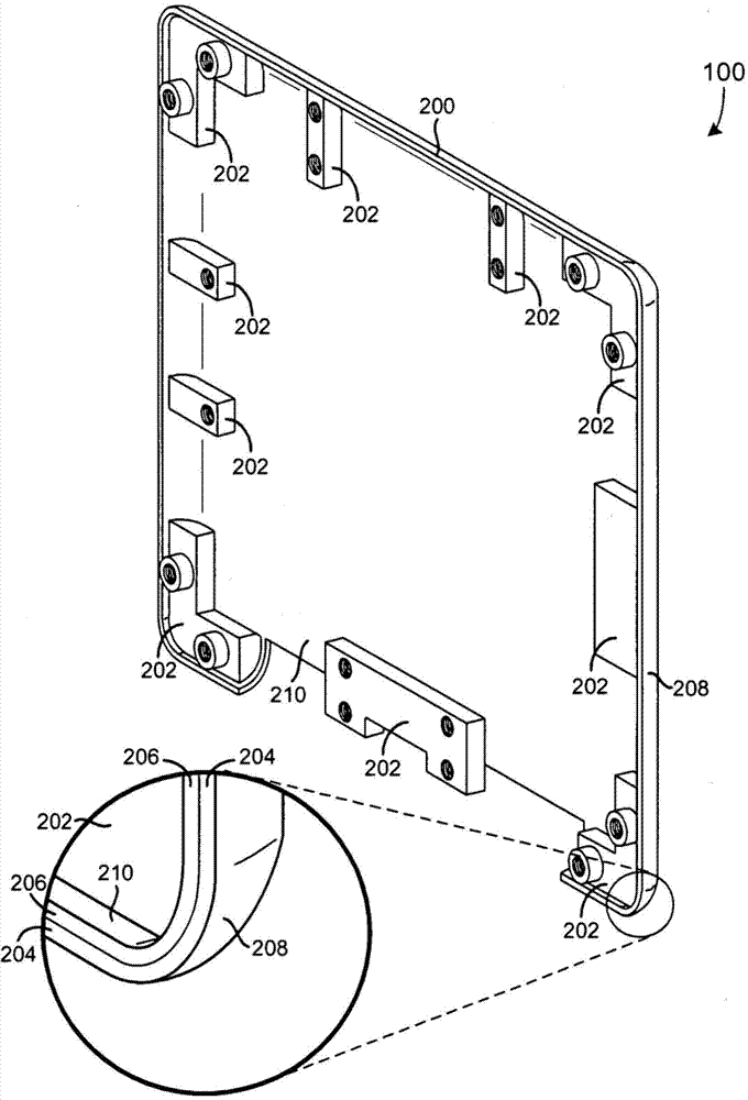
图2是显示为从图1的膝上型计算机卸下的该示例外壳的透视图;Figure 2 is a perspective view of the example housing shown disassembled from the laptop computer of Figure 1;
图3是示出了用于制造图1的外壳的一种示例方法的图;FIG. 3 is a diagram illustrating an example method for manufacturing the housing of FIG. 1;
图4是概述用于制造图1的外壳的一种示例方法的流程图;FIG. 4 is a flowchart outlining an example method for manufacturing the housing of FIG. 1;
图5是示出了用于制造图1的外壳的另一示例方法的图;FIG. 5 is a diagram illustrating another example method for manufacturing the housing of FIG. 1;
图6是概述用于制造图1的外壳的另一示例方法的流程图;6 is a flowchart outlining another example method for manufacturing the housing of FIG. 1;
图7是一个替代外壳的透视图;Figure 7 is a perspective view of an alternative housing;
图8是示出了用于制造图7的外壳的一种示例方法的图;FIG. 8 is a diagram illustrating an example method for manufacturing the housing of FIG. 7;
图9是概述用于制造图7的外壳的一种示例方法的流程图;FIG. 9 is a flowchart outlining an example method for manufacturing the housing of FIG. 7;
图10是示出了用于制造图7的外壳的另一示例方法的图;而FIG. 10 is a diagram illustrating another example method for manufacturing the housing of FIG. 7; and
图11是概述用于制造图7的外壳的另一示例方法的流程图。FIG. 11 is a flowchart outlining another example method for manufacturing the housing of FIG. 7 .
具体实施方式 Detailed ways
本发明通过提供具有包层金属壳体和附接于此的多个安装结构的装置外壳,来克服与现有技术相关联的问题。在以下描述中,给出了若干特定细节(例如,主机装置的细节),以提供对本发明的彻底理解。然而,本领域的技术员应该意识到本发明也可以偏离这些特定细节而实施。在其它情况中,众所周知的制造实践(例如,塑料注射成型、模具加工等)和部件的细节已被省略,以免不必要地模糊本发明。The present invention overcomes the problems associated with the prior art by providing a device housing having a clad metal housing and a plurality of mounting structures attached thereto. In the following description, several specific details are given (eg, details of a host device) in order to provide a thorough understanding of the present invention. It will be appreciated, however, by those skilled in the art, that the present invention may be practiced without these specific details. In other instances, well-known manufacturing practices (eg, plastic injection molding, tooling, etc.) and details of components have been omitted so as not to unnecessarily obscure the present invention.
图1示出了外壳100的透视图,所述外壳100在该特定实施例中通过示例图示为用于膝上型计算机102的机壳的一部分。如图所示,计算机102包括基座组件104和显示组件106,它们通过一些适当的器件(比如铰链组件等)可枢转地联接至彼此。FIG. 1 shows a perspective view of an
基座组件104包括机壳108、键盘110、触摸板112和各种其它众所周知的部件(未示出),比如框体、主板、I/O端口、硬盘驱动器、电池等。机壳108包括顶部外壳114和底部外壳116,它们彼此联接以容纳键盘110、触摸板112和基座组件104的未示出的各种其它部件。顶部外壳114包括带槽框结构或者面板结构,其限定出与键盘110和触摸板112对齐的开口。虽然未示出,但是底部外壳116可能会包括封装计算机102的电池的可拆卸电池盖(和其它众所周知的膝上型计算机部件)。The
显示组件106包括机壳118和各种其它众所周知的翻转屏显示部件(未示出),比如液晶显示屏(LCD)、框体、扬声器、电路基板/部件、摄像头模块等。机壳118包括前侧外壳120和后侧外壳100,它们可固定地安装在显示组件106的两相反侧,以便一起容纳未示出的上述翻转屏显示部件。前侧外壳120是可固定地安装至显示组件106的前侧以覆盖LCD面板的周缘的带槽框。后侧外壳100固定地联接至例如显示组件106的框体和/或一些其它适当的结构。The
图2是后侧外壳100的透视图,图示为从计算机102的显示组件106的背面卸下。此外,图2还示出了外壳100的角部的放大视图。外壳100包括壳体200和多个三维安装结构202。当外壳100安装至显示组件106时,壳体200覆盖并保护显示组件106的下方内部部件,并且还有助于计算机102的整体美观。安装结构202是联接至壳体200以促进外壳100向显示组件106的紧固的三维结构(例如,螺丝凸台,螺母/螺栓座、卡扣件等)。结构202还可以包括能够并入金属壳体外壳中的任何其它类型的结构,比如支撑架(scaffolding)、加强肋、肋条等。FIG. 2 is a perspective view of
壳体200是多层复合金属结构,其包括独立的第一金属层204和独立的第二金属层206,两者间具有直接结合。在该特定实施例中,壳体200由钛-铝包层金属构成,其中第一金属层204为钛而第二金属层206为铝。因此,层204、206分别限定出壳体200的外表面208和内表面210。在第一金属层204由钛或其合金构成的情况下,壳体200的外表面208比常规的全铝外壳更加耐受损坏(即表面玷污、局部屈曲等)。
虽然图2的视图中未示出,但是外表面208是使用已知的钛装饰技术装饰过的。例如,外表面208通过阳极化处理得到着色,并且包括通过钛激光打标形成在其上的装饰特征212(图1中可见)。本领域的技术人员将意识到的是特征212的具体装饰设计特征(例如,颜色、尺寸、形状等)将取决于特定应用,因此不是本发明的实质性方面。因此,特征212可以是任何类型的激光打标的符号、图像、图标、信息、贴花、图案等。Although not shown in the view of FIG. 2 , the
安装结构202是三维模塑成型塑料结构(例如,螺丝凸台、卡扣件、壳体加强肋等),其附接至壳体200以促进外壳100向显示组件106的安装。在该特定实施例中,结构202通过纳米成型技术(NMT)直接地形成在内表面210上,从而在两者间实现直接的机械结合。替代地,结构202可以在被附接至内表面210前形成。例如,所述结构可以是通过粘结剂、双面胶带等固定至内表面210的模塑成型塑料部件。Mounting
图3是示出了用于制造外壳100的一个示例方法300的图。方法300包括第一阶段302、第二阶段304、第三阶段306、第四阶段308、第五阶段310和第六阶段312。FIG. 3 is a diagram illustrating an
阶段302包括形成由其构成壳体200的冷轧钛/铝包层片状金属314。在该特定实施例中,通过使钛片状金属316和铝片状金属318同时经过滚筒组件320,来形成钛/铝包层片状金属314。
阶段304包括从钛/铝包层片状金属314形成壳体200。在该特定实施例中,壳体200是通过模压钛/铝包层片状金属314形成的。
第三阶段306包括使壳体200准备好进行后续的NMT工艺。在该特定实施例中,壳体200经受T处理,以在内表面210上生成微型凹陷(例如,小孔、间隙等)。总的来说,T处理涉及一个或多个工艺,其中内表面210暴露于各种蚀刻和/或清洁化学制品。如本示例中示出的,壳体200被浸入蚀刻铝的碱性水溶液池322中。然而,应该指出的是,本发明的蚀刻工艺并非必须局限于T处理。相反,任意适当的蚀刻工艺或者工艺序列,现在已知的或者还未公开的,都可以用于准备壳体200以用于NMT工艺。The
第四阶段308包括形成安装结构202。在该特定实施例中,结构202通过NMT直接地形成在壳体200的内表面210上,从而直接地联接至壳体200的内表面210。在通过NMT形成结构202时,低粘度热塑性(例如,聚苯硫醚树脂塑料,聚对苯二甲酸丁二酯)熔体直接地注射成型在内表面210上,然后被允许冷凝成结构202的形状。在注射工艺期间,热塑性熔体在阶段306期间渗入形成在内表面210上的凹陷中,使得在冷凝时,结构202的一些部分永久地锚定至从而机械地结合至层206。The
第五阶段310包括对壳体200的外表面208着色。在本示例方法中,外表面208通过阳极化处理而着色。The
第六阶段312包括在外表面208上形成装饰特征212。在本示例方法中,特征212通过激光打标形成在外表面上。The
图4是概述用于制造电子装置外壳的示例方法400的流程图。在第一步402中,设置可成型基板。然后,在第二步404中,设置至少具有第一金属层和第二金属层的多层片状金属。接下来,在第三步406中,将多层片状金属形成为金属壳体。然后,在第四步408中,使壳体受到NMT预处理工艺。接下来,在第五步410中,使可成型基板直接地成型在壳体的第一层上,成为三维安装结构的形状。然后,在第六步412中,使壳体受到阳极化处理。最后,在第七步414中,通过激光打标在壳体上形成装饰特征。FIG. 4 is a flowchart outlining an
图5是示出了用于制造外壳100的替代方法500的图。方法500包括第一阶段502、第二阶段504、第三阶段506、第四阶段508、第五阶段510和第六阶段512。FIG. 5 is a diagram illustrating an
阶段502包括形成由其构成壳体200的冷轧钛/铝包层片状金属514。在该特定方法中,通过使钛片状金属516和铝片状金属518同时经过滚筒组件520,来形成钛/铝包层片状金属514。
阶段504包括从钛/铝包层片状金属514形成壳体200。在该特定方法中,壳体200是通过模压钛/铝包层片状金属514形成的。
阶段506包括形成安装结构202。在该特定方法中,安装结构202在被附接至壳体200前形成。例如,安装结构通过注射成型形成。
阶段508包括联接安装结构202与壳体200。在该特定方法中,安装结构202通过一些适当的手段,比如粘结剂、环氧树脂、双面粘胶带等,直接地附接至内表面210。
阶段510包括对壳体200的外表面208着色。在该特定方法中,外表面208通过阳极化处理而着色。
第六阶段512包括在外表面208上形成装饰特征212。在该特定方法中,特征212通过激光打标形成在外表面上。The
图6是概述用于制造电子装置外壳的示例方法600的流程图。在第一步602中,设置具有第一金属层和第二金属层的多层片状金属。然后,在第二步604中,设置三维安装结构。接下来,在第三步606中,设置粘结剂。然后,在第四步608中,将多层片状金属形成为金属壳体。然后,在第五步610中,通过粘结剂将安装结构直接地附接至壳体的第一层。然后,在第六步612中,使壳体受到阳极化处理。最后,在第七步614中,通过例如激光打标在壳体上形成装饰特征。FIG. 6 is a flowchart outlining an
图7是一替代外壳700的透视图,示出了外壳700的一个角部的放大视图。外壳700包括壳体701和多个三维安装结构702。FIG. 7 is a perspective view of an
壳体701是多层复合金属结构,其包括独立的第一金属层704、独立的第二金属层706和独立的第三金属层708。在该特定实施例中,壳体701由钛-铝包层金属构成,其中第一金属层704为钛,第二金属层706为铝,并且第三金属层708为钛。因此,层704、708分别限定出壳体701的外表面710和内表面712。在第一金属层704由钛或其合金构成的情况下,壳体701的外表面710比常规的全铝外壳更加耐受损坏(即表面玷污、局部屈曲等)。The
虽然未示出,但是外表面710通过已知的钛装饰技术得到装饰。例如,外表面710通过阳极化处理得到着色,并且包括通过钛激光打标形成在其上的装饰特征212(图1中可见)。Although not shown,
安装结构702是三维模塑成型塑料结构(例如,螺丝凸台、卡扣件、壳体加强肋等),其附接至壳体701以促进外壳700向显示组件106的安装。在该特定实施例中,结构702通过纳米成型技术(NMT)直接地形成在内表面712上,从而在两者间实现直接的机械结合。替代地,结构702可以预先形成(即,在被附接至内表面712前形成)。例如,结构702可以是通过粘结剂、环氧树脂、双面胶带或者任意其它适当的手段固定至内表面712的模塑成型塑料部件。Mounting
图8是示出了用于制造根据本发明的另一实施例的外壳700的一个示例方法800的图。方法800包括第一阶段802、第二阶段804、第三阶段806、第四阶段808、第五阶段810和第六阶段812。FIG. 8 is a diagram illustrating an
阶段802包括形成由其构成壳体701的冷轧钛/铝包层片状金属814。在该特定方法中,通过使钛片状金属816、铝片状金属818和钛片状金属820同时经过滚筒组件822,来形成钛/铝包层片状金属814。
阶段804包括从钛/铝包层片状金属814形成壳体701。在该特定方法中,壳体701是通过将钛/铝包层片状金属814模压成期望形状而形成的。
第三阶段806包括使壳体701准备好进行后续的NMT工艺。在该特定方法中,壳体701经受T处理,以在内表面712上生成微型凹陷(例如,小孔、间隙等)。总的来说,T处理涉及一个或多个工艺,其中内表面712暴露于各种蚀刻和/或清洁化学制品。如本示例中示出的,壳体701被浸入蚀刻内表面712的碱性水溶液池824中。然而,应该指出的是,本发明的蚀刻工艺并非必须局限于T处理。相反,可以实施任意适当的蚀刻工艺或者工艺序列。The
第四阶段808包括形成安装结构702。在该特定方法中,结构702通过NMT直接地形成在壳体701的内表面712上,从而直接地联接至壳体701的内表面712。为了通过NMT形成结构702,低粘度热塑性(例如,聚苯硫醚树脂塑料,聚对苯二甲酸丁二酯)熔体直接地注射成型在内表面712上,然后被允许冷凝成结构702的形状。在注射工艺期间,热塑性熔体在阶段806期间渗入形成在内表面712上的凹陷中,使得在冷凝时,结构702的一些部分永久地锚定至从而机械地结合至层708。The
第五阶段810包括对壳体701的外表面710着色。在该特定方法中,外表面710通过阳极化处理而着色。The
第六阶段812包括在外表面710上形成装饰特征212。在该特定方法中,特征212通过激光打标形成在外表面710上。
图9是概述用于制造电子装置外壳的另一示例方法900的流程图。在第一步902中,设置可成型基板。然后,在第二步904中,设置具有第一金属层、第二金属层和第三金属层的多层片状金属。接下来,在第三步906中,将多层片状金属形成为金属壳体。然后,在第四步908中,使壳体受到NMT预处理工艺。接下来,在第五步910中,使可成型基板直接地成型在壳体的第一层上,成为三维安装和/或支承结构的形状。然后,在第六步912中,使壳体受到阳极化处理。最后,在第七步914中,通过激光打标在壳体上形成装饰特征。FIG. 9 is a flowchart outlining another
图10是示出了用于制造外壳700的另一示例方法1000的图。方法1000包括第一阶段1002、第二阶段1004、第三阶段1006、第四阶段1008、第五阶段1010和第六阶段1012。FIG. 10 is a diagram illustrating another
阶段1002包括形成由其构成壳体701的冷轧钛/铝包层片状金属1014。在该特定方法中,通过使钛片状金属1016、铝片状金属1018和钛片状金属1020同时经过滚筒组件1022,来形成钛/铝包层片状金属1014。
阶段1004包括从钛/铝包层片状金属1014形成壳体701。在该特定方法中,壳体701是通过将钛/铝包层片状金属1014模压成期望形状而形成的。
阶段1006包括形成安装结构702。在该特定方法中,安装结构702在被附接至壳体701前形成。例如,安装结构可以通过注射成型形成。
阶段1008包括将安装结构702固定至壳体701。在该特定方法中,安装结构702通过例如粘结剂、环氧树脂、双面粘胶带或者任意其它适当的固定手段直接地附接至内表面712。
阶段1010包括对壳体701的外表面710着色。在该特定方法中,外表面710通过阳极化处理而着色。
第六阶段1012包括在外表面710上形成装饰特征212。在该特定方法中,特征212通过激光打标形成在外表面710上。
图11是概述用于制造电子装置外壳的另一示例方法1100的流程图。在第一步1102中,设置具有第一金属层、第二金属层和第三金属层的多层片状金属。然后,在第二步1104中,设置三维安装结构。接下来,在第三步1106中,设置粘结剂。然后,在第四步1108中,将多层片状金属形成为金属壳体。然后,在第五步1110中,通过粘结剂将安装结构直接地附接至壳体的第一层。然后,在第六步1112中,使壳体受到阳极化处理。最后,在第七步1114中,通过例如激光打标在壳体上形成装饰特征。11 is a flowchart outlining another
本发明的特定实施例的描述现在结束了。许多所描述的特征可能被取代、改变或者省略,而不背离本发明的范围。例如,替代主机装置(例如,移动电话、PDA、相机等)可以取代膝上型计算机102。作为另一示例,替代类型的包层片状金属可以取代本文所述的示例性包层片状金属。从所示特定实施例发生的这些和其它偏差对本领域的技术人员来说将是显而易见的,特别是鉴于以上公开。The description of specific embodiments of the invention now concludes. Many of the described features may be substituted, changed or omitted without departing from the scope of the invention. For example, an alternate host device (eg, mobile phone, PDA, camera, etc.) may replace
Claims (52)
Applications Claiming Priority (3)
| Application Number | Priority Date | Filing Date | Title |
|---|---|---|---|
| US28926609P | 2009-12-22 | 2009-12-22 | |
| US61/289,266 | 2009-12-22 | ||
| PCT/US2010/003233 WO2011087487A1 (en) | 2009-12-22 | 2010-12-22 | Enclosure of anodized multi-layer metallic shell with molded plastic scaffolding and method of manufacture |
Publications (2)
| Publication Number | Publication Date |
|---|---|
| CN102763295A true CN102763295A (en) | 2012-10-31 |
| CN102763295B CN102763295B (en) | 2015-12-16 |
Family
ID=44304525
Family Applications (1)
| Application Number | Title | Priority Date | Filing Date |
|---|---|---|---|
| CN201080063429.5A Expired - Fee Related CN102763295B (en) | 2009-12-22 | 2010-12-22 | There is shell and the manufacture method of the anodization multiple layer metal housing of moulded plastic bracing frame |
Country Status (3)
| Country | Link |
|---|---|
| US (1) | US8681485B2 (en) |
| CN (1) | CN102763295B (en) |
| WO (1) | WO2011087487A1 (en) |
Cited By (4)
| Publication number | Priority date | Publication date | Assignee | Title |
|---|---|---|---|---|
| CN104066293B (en) * | 2013-03-21 | 2017-02-08 | 宏达国际电子股份有限公司 | Electronic device casing and manufacturing method thereof |
| US9655261B2 (en) | 2013-03-21 | 2017-05-16 | Htc Corporation | Casing of electronic device and method of manufacturing the same |
| US9716307B2 (en) | 2012-11-08 | 2017-07-25 | Htc Corporation | Mobile device and antenna structure |
| CN114829101A (en) * | 2020-01-08 | 2022-07-29 | 惠普发展公司,有限责任合伙企业 | Electronic device housing with hydrophobic coating |
Families Citing this family (27)
| Publication number | Priority date | Publication date | Assignee | Title |
|---|---|---|---|---|
| US8367304B2 (en) | 2008-06-08 | 2013-02-05 | Apple Inc. | Techniques for marking product housings |
| US9173336B2 (en) | 2009-05-19 | 2015-10-27 | Apple Inc. | Techniques for marking product housings |
| US8809733B2 (en) * | 2009-10-16 | 2014-08-19 | Apple Inc. | Sub-surface marking of product housings |
| US20110089039A1 (en) * | 2009-10-16 | 2011-04-21 | Michael Nashner | Sub-Surface Marking of Product Housings |
| US10071583B2 (en) * | 2009-10-16 | 2018-09-11 | Apple Inc. | Marking of product housings |
| US9845546B2 (en) * | 2009-10-16 | 2017-12-19 | Apple Inc. | Sub-surface marking of product housings |
| US20140061084A1 (en) * | 2010-08-20 | 2014-03-06 | Cyber Acoustics, Llc | Portable electronic device protector |
| US8724285B2 (en) | 2010-09-30 | 2014-05-13 | Apple Inc. | Cosmetic conductive laser etching |
| US20120248001A1 (en) | 2011-03-29 | 2012-10-04 | Nashner Michael S | Marking of Fabric Carrying Case for Portable Electronic Device |
| US9280183B2 (en) | 2011-04-01 | 2016-03-08 | Apple Inc. | Advanced techniques for bonding metal to plastic |
| US20130075126A1 (en) * | 2011-09-27 | 2013-03-28 | Michael S. Nashner | Laser Bleached Marking of Dyed Anodization |
| KR101346083B1 (en) * | 2012-04-26 | 2013-12-31 | 엘지디스플레이 주식회사 | Display Device |
| US8879266B2 (en) | 2012-05-24 | 2014-11-04 | Apple Inc. | Thin multi-layered structures providing rigidity and conductivity |
| US9578769B2 (en) * | 2012-05-29 | 2017-02-21 | Apple Inc. | Components of an electronic device and methods for their assembly |
| US9445517B2 (en) | 2012-06-04 | 2016-09-13 | Google Inc. | Etched multi-layer sheets |
| US10071584B2 (en) | 2012-07-09 | 2018-09-11 | Apple Inc. | Process for creating sub-surface marking on plastic parts |
| US9314871B2 (en) | 2013-06-18 | 2016-04-19 | Apple Inc. | Method for laser engraved reflective surface structures |
| US9434197B2 (en) | 2013-06-18 | 2016-09-06 | Apple Inc. | Laser engraved reflective surface structures |
| CN103643277B (en) * | 2013-12-27 | 2016-01-13 | 东莞捷荣技术股份有限公司 | A kind of aluminium shell based on nanometer forming process and anode oxidation method thereof |
| JP6264905B2 (en) * | 2014-01-31 | 2018-01-24 | 住友電気工業株式会社 | Composite member and method of manufacturing composite member |
| WO2018045484A1 (en) * | 2016-09-06 | 2018-03-15 | Apple Inc. | Laser bleach marking of an anodized surface |
| US10433048B2 (en) | 2017-08-31 | 2019-10-01 | Apple Inc. | Micro speaker having a hermetically sealed acoustic chamber with increased volume |
| US11090876B2 (en) | 2018-09-18 | 2021-08-17 | Flex Ltd. | Assembly of sub-components by compression molding |
| US10999917B2 (en) | 2018-09-20 | 2021-05-04 | Apple Inc. | Sparse laser etch anodized surface for cosmetic grounding |
| US10908649B2 (en) * | 2019-05-20 | 2021-02-02 | Microsoft Technology Licensing, Llc | Interchangeable housing component for portable computing devices |
| US12324114B2 (en) | 2021-09-24 | 2025-06-03 | Apple Inc. | Laser-marked electronic device housings |
| US20240373574A1 (en) * | 2023-05-05 | 2024-11-07 | Apple Inc. | Electronic device including clad components |
Citations (9)
| Publication number | Priority date | Publication date | Assignee | Title |
|---|---|---|---|---|
| US20050149860A1 (en) * | 2002-12-27 | 2005-07-07 | Casio Computer Co., Ltd. | Electronic device manufacture support apparatus, manufacture client terminal device, and recording medium |
| US6996425B2 (en) * | 2000-11-16 | 2006-02-07 | Nec Corporation | Cellular phone housing |
| CN1852640A (en) * | 2006-04-05 | 2006-10-25 | 宏碁股份有限公司 | Shell structure and manufacturing method thereof |
| US20070256850A1 (en) * | 2006-05-04 | 2007-11-08 | Hansen Cynthia L | Tamper resistant electrical outlet cover assembly |
| US20080224358A1 (en) * | 2005-09-15 | 2008-09-18 | John Rogers | Nano-Molding Process |
| CN101416571A (en) * | 2006-04-03 | 2009-04-22 | 三菱电机株式会社 | Electronic equipment housing |
| US20090190290A1 (en) * | 2008-01-24 | 2009-07-30 | Stephen Brian Lynch | Methods and Systems for Forming Housings From Multi-Layer Materials |
| US20090194308A1 (en) * | 2008-02-01 | 2009-08-06 | Fih (Hong Kong) Limited | Metal housing |
| US20090275370A1 (en) * | 2007-01-04 | 2009-11-05 | Schlub Robert W | Handheld electronic devices with isolated antennas |
Family Cites Families (10)
| Publication number | Priority date | Publication date | Assignee | Title |
|---|---|---|---|---|
| US3122598A (en) * | 1960-11-03 | 1964-02-25 | Foster Grant Co Inc | Plastic decorating method |
| US6620371B1 (en) * | 1998-05-22 | 2003-09-16 | Patent Holding Company | Method of manufacturing an in-mold laminate component |
| US6768654B2 (en) * | 2000-09-18 | 2004-07-27 | Wavezero, Inc. | Multi-layered structures and methods for manufacturing the multi-layered structures |
| US6574096B1 (en) * | 2000-09-29 | 2003-06-03 | Apple Computer, Inc. | Use of titanium in a notebook computer |
| JP4195881B2 (en) | 2002-11-08 | 2008-12-17 | 大成プラス株式会社 | Aluminum alloy / resin composite and method for producing the same |
| KR100827916B1 (en) * | 2002-11-08 | 2008-05-07 | 다이세이 플라스 가부시끼가이샤 | Composite of aluminum alloy and resin composition and process for producing the same |
| JP3939667B2 (en) | 2003-03-05 | 2007-07-04 | 大成プラス株式会社 | Aluminum alloy container with bonding structure and manufacturing method thereof |
| WO2005109984A2 (en) | 2004-05-18 | 2005-11-24 | Bang & Olufsen A/S | A process for the manufacture of a hybrid element comprising a metal skin |
| CN101554826A (en) * | 2008-04-11 | 2009-10-14 | 深圳富泰宏精密工业有限公司 | Manufacturing method of casing and casing manufactured therefrom |
| US8646637B2 (en) * | 2008-04-18 | 2014-02-11 | Apple Inc. | Perforated substrates for forming housings |
-
2010
- 2010-12-22 WO PCT/US2010/003233 patent/WO2011087487A1/en not_active Ceased
- 2010-12-22 CN CN201080063429.5A patent/CN102763295B/en not_active Expired - Fee Related
- 2010-12-22 US US12/928,941 patent/US8681485B2/en active Active
Patent Citations (9)
| Publication number | Priority date | Publication date | Assignee | Title |
|---|---|---|---|---|
| US6996425B2 (en) * | 2000-11-16 | 2006-02-07 | Nec Corporation | Cellular phone housing |
| US20050149860A1 (en) * | 2002-12-27 | 2005-07-07 | Casio Computer Co., Ltd. | Electronic device manufacture support apparatus, manufacture client terminal device, and recording medium |
| US20080224358A1 (en) * | 2005-09-15 | 2008-09-18 | John Rogers | Nano-Molding Process |
| CN101416571A (en) * | 2006-04-03 | 2009-04-22 | 三菱电机株式会社 | Electronic equipment housing |
| CN1852640A (en) * | 2006-04-05 | 2006-10-25 | 宏碁股份有限公司 | Shell structure and manufacturing method thereof |
| US20070256850A1 (en) * | 2006-05-04 | 2007-11-08 | Hansen Cynthia L | Tamper resistant electrical outlet cover assembly |
| US20090275370A1 (en) * | 2007-01-04 | 2009-11-05 | Schlub Robert W | Handheld electronic devices with isolated antennas |
| US20090190290A1 (en) * | 2008-01-24 | 2009-07-30 | Stephen Brian Lynch | Methods and Systems for Forming Housings From Multi-Layer Materials |
| US20090194308A1 (en) * | 2008-02-01 | 2009-08-06 | Fih (Hong Kong) Limited | Metal housing |
Cited By (9)
| Publication number | Priority date | Publication date | Assignee | Title |
|---|---|---|---|---|
| US9716307B2 (en) | 2012-11-08 | 2017-07-25 | Htc Corporation | Mobile device and antenna structure |
| US10490883B2 (en) | 2012-11-08 | 2019-11-26 | Htc Corporation | Mobile device and antenna structure |
| US10516202B2 (en) | 2012-11-08 | 2019-12-24 | Htc Corporation | Mobile device and antenna structure |
| US10833398B2 (en) | 2012-11-08 | 2020-11-10 | Htc Corporation | Mobile device and antenna structure |
| US10879591B2 (en) | 2012-11-08 | 2020-12-29 | Htc Corporation | Mobile device and antenna structure |
| US11038258B2 (en) | 2012-11-08 | 2021-06-15 | Htc Corporation | Mobile device and antenna structure |
| CN104066293B (en) * | 2013-03-21 | 2017-02-08 | 宏达国际电子股份有限公司 | Electronic device casing and manufacturing method thereof |
| US9655261B2 (en) | 2013-03-21 | 2017-05-16 | Htc Corporation | Casing of electronic device and method of manufacturing the same |
| CN114829101A (en) * | 2020-01-08 | 2022-07-29 | 惠普发展公司,有限责任合伙企业 | Electronic device housing with hydrophobic coating |
Also Published As
| Publication number | Publication date |
|---|---|
| WO2011087487A1 (en) | 2011-07-21 |
| US8681485B2 (en) | 2014-03-25 |
| CN102763295B (en) | 2015-12-16 |
| US20110186455A1 (en) | 2011-08-04 |
Similar Documents
| Publication | Publication Date | Title |
|---|---|---|
| CN102763295B (en) | There is shell and the manufacture method of the anodization multiple layer metal housing of moulded plastic bracing frame | |
| CN206698539U (en) | Housings for electronic devices and electronic devices | |
| US7385806B2 (en) | Combination housing of a notebook computer | |
| CN102224473B (en) | Unified top case for portable computers | |
| EP2453635B1 (en) | Portable terminal and method for manufacturing the same | |
| CN204291096U (en) | A kind of metal center mobile terminal | |
| JP2013508818A (en) | Portable computing system | |
| CN105302240A (en) | Component assembly | |
| CN103507211A (en) | Method and apparatus for processing housing | |
| CN205004435U (en) | Mobile terminal with front camera and large LCD | |
| US20190104628A1 (en) | Case, method of manufacturing the same and electronic device | |
| CN101895710B (en) | A kind of TV cover and manufacturing method thereof | |
| CN111246068A (en) | Camera decorative ring and processing method thereof, and electronic equipment | |
| CN201118680Y (en) | Mobile phone shell and mobile phone with the shell | |
| CN117642265A (en) | Hybrid components for automotive applications and methods of manufacturing hybrid components | |
| CN107708356B (en) | Shell manufacturing method, shell and electronic equipment | |
| CN107608453A (en) | Sheet material, method for preparing sheet material, housing, and mobile terminal | |
| KR20080094439A (en) | Dissimilar Metal Mold Casting Method | |
| CN207340353U (en) | Plate, housing and mobile terminal | |
| TWI446854B (en) | Electronic device and the molding method for the metallic housing thereof | |
| CN204833086U (en) | Notebook computer metal casing | |
| CN107708352A (en) | Shell manufacturing method, shell and electronic device | |
| CN107744932B (en) | Shell manufacturing method, shell and electronic equipment | |
| CN108493599B (en) | Manufacturing method of printed antenna assembly, printed antenna assembly and electronic equipment | |
| CN108235628B (en) | Middle frame manufacturing method, middle frame and electronic equipment |
Legal Events
| Date | Code | Title | Description |
|---|---|---|---|
| C06 | Publication | ||
| PB01 | Publication | ||
| C10 | Entry into substantive examination | ||
| SE01 | Entry into force of request for substantive examination | ||
| C14 | Grant of patent or utility model | ||
| GR01 | Patent grant | ||
| CF01 | Termination of patent right due to non-payment of annual fee |
Granted publication date: 20151216 Termination date: 20161222 |
|
| CF01 | Termination of patent right due to non-payment of annual fee |