Summary of the invention
Therefore, the present invention is conceived to the problems referred to above point, its purpose be to provide a kind of can be when keeping high-precision temperature-compensating, realize the temperature compensating type oscillator of economize on electricity and the electronic equipment that is equipped with this oscillator with easy structure.
The present invention accomplishes at least a portion that solves in the above-mentioned problem, and it can be realized as following application examples.
Application examples 1
A kind of temperature compensating type oscillator, it has: temperature sensor, it is used for output and the corresponding detected temperatures voltage of temperature; Temperature-compensation circuit, it is according to said detected temperatures voltage and the output temperature bucking voltage; Voltage control oscillating circuit, the oscillator signal that its output has been carried out temperature-compensating according to the said temperature-compensated voltage of being imported; Said temperature compensating type oscillator is characterised in that to possess: output circuit, and it exports the conducting cut-off signal according to the size of the voltage variety of said detected temperatures voltage in required time and the magnitude relationship between the reference voltage; Switching circuit, it accepts said conducting cut-off signal, thus conducting disconnection control is carried out in the supply of the electrical power of the said temperature-compensation circuit of subtend; Sampling hold circuit; It accepts said conducting cut-off signal; Thereby between following state by switching controls; Promptly; Be connected with said temperature-compensation circuit, and in the said temperature-compensated voltage that keeps said temperature-compensation circuit to export, export said temperature-compensated voltage the state of said voltage control oscillating circuit to, with cut off with being connected of said temperature-compensation circuit in, the said temperature-compensated voltage that is kept exported to the state of said voltage control oscillating circuit.
According to said structure; Can be based on the size of the voltage variety of the detected detected temperatures voltage of temperature sensor; And judge whether implementing temperature-compensating; When the size of voltage variety during, thereby temperature-compensation circuit is driven to voltage control oscillating circuit output temperature bucking voltage, and in sampling hold circuit, keep temperature-compensated voltage greater than reference voltage; When the size of voltage variety during, stop driving, and export the temperature-compensated voltage that is kept in the sampling hold circuit to voltage control oscillating circuit temperature-compensated voltage less than reference voltage.Therefore, become the temperature compensating type oscillator that when keeping high-precision temperature-compensating, with easy structure, to realize economize on electricity.
Application examples 2
Like application examples 1 described temperature compensating type oscillator, it is characterized in that said output circuit has: low pass filter, it is transfused to said detected temperatures voltage; Differential amplifier circuit, it is through carrying out differential amplification to the output of said temperature sensor and the output of said low pass filter, thus output and the corresponding voltage of said voltage variety; Absolute value circuit, it is through the voltage of output as the absolute value of said differential amplifier circuit output, thus the big or small corresponding voltage of output and said voltage variety; Comparator, it will represent the output of said absolute value circuit and the signal of the magnitude relationship between the said reference voltage, export as said conducting cut-off signal.
According to said structure; Because the detected temperatures voltage before the certain hour of low pass filter output current time; Therefore in absolute value circuit; Can calculate current detected temperatures voltage, and the certain hour of current time before detected temperatures voltage between the size of difference, i.e. the size of the voltage variety of detected temperatures voltage.Therefore, can be in the size of the voltage variety that calculates detected temperatures voltage with easy structure, output conducting cut-off signal.
Application examples 3
Like application examples 1 described temperature compensating type oscillator, it is characterized in that said output circuit has: timer, it is output drive signal with the fixed cycle; Second sampling hold circuit; It accepts said drive signal; Thereby can between following state, switch; That is, be connected with said temperature sensor and when keeping said detected temperatures voltage, the state of the said detected temperatures voltage output of output, the state of exporting in the time of with being connected of cut-out and said temperature sensor, with the said detected temperatures voltage that is kept; Said differential amplifier circuit, it is through carrying out differential amplification to the output of said temperature sensor and the output of said second sampling hold circuit, thus output and the corresponding voltage of said voltage variety; Absolute value circuit, it becomes the voltage of absolute value of the output of said differential amplifier circuit through output, thus the big or small corresponding voltage of output and said voltage variety; Comparator, it will represent the output of said absolute value circuit and the signal of the magnitude relationship between the said reference voltage, export as said conducting cut-off signal.
According to said structure, can be through changing the cycle of timer, thus at random set counting period to the size of the voltage variety of detected temperatures voltage.
Application examples 4
Like application examples 2 or 3 described temperature compensating type oscillators; It is characterized in that said output circuit has the cut-out circuit, when said detected temperatures voltage does; During value between the first threshold that is set in advance and second threshold voltage that is set in advance; Said cut-out circuit cuts off said conducting cut-off signal, and wherein, said second threshold voltage is the value that is higher than said first threshold voltage.
In said structure; Owing to be set to; For example and the corresponding temperature of first threshold voltage and and the corresponding temperature of second threshold voltage between become; The temperature characterisitic of the cycle of oscillation of voltage control oscillating circuit have very mild characteristic the zone (near the temperature range the extreme value of the curve of frequency-temperature characteristic and this extreme value, promptly therebetween the amplitude of variation of frequency-temperature characteristic in the stability of the desired frequency-temperature characteristic of temperature compensating type oscillator with interior zone), thereby in this temperature province, need not carry out renewal to temperature-compensated voltage; Therefore, need not carry out driving to temperature-compensation circuit.Therefore, when the detected temperature of temperature sensor is in this temperature province, stop driving, thereby can reduce electric power consumption significantly temperature-compensation circuit.
Application examples 5
Like application examples 2 or 3 described temperature compensating type oscillators, it is characterized in that said output circuit has: delay circuit, it is transfused to said conducting cut-off signal, and output makes the inhibit signal of the change in voltage delay of said conducting cut-off signal; The exclusive disjunction circuit, the signal that its exclusive disjunction that will become said conducting cut-off signal and said inhibit signal is separated exports said switching circuit to as said conducting cut-off signal; With computing circuit, its signal of separating with computing that will become said conducting cut-off signal and said inhibit signal exports said sampling hold circuit to as said conducting cut-off signal.
According to said structure, the unlatching of the driving of sampling hold circuit is later than the unlatching of the driving of temperature-compensation circuit, and the driving of sampling hold circuit close closing early than the driving of temperature-compensation circuit.Thus; Temperature-compensation circuit can be till opening to sampling hold circuit during in make the output of temperature-compensated voltage stable; And, therefore can implement maintenance effectively to the temperature-compensated voltage of exporting by temperature-compensation circuit owing to before temperature-compensation circuit is opened, sampling hold circuit is closed.
Application examples 6
Like the described temperature compensating type oscillator of arbitrary example in the application examples 1 to 3; It is characterized in that; Between said temperature-compensation circuit and the said sampling hold circuit or between said sampling hold circuit and said voltage control oscillating circuit, dispose second low pass filter.
After just temperature-compensation circuit being made as conducting state, sampling hold circuit will switch to from the temperature-compensated voltage that is kept from the temperature-compensated voltage of the new input of temperature-compensation circuit.Thus, when this switched, temperature-compensated voltage was discontinuous on time orientation, thereby might cause negative effect to voltage control oscillating circuit.Therefore, through said structure, the time of the temperature-compensated voltage of new input is become gently, thereby alleviate burden voltage control oscillating circuit.
Application examples 7
A kind of electronic equipment is characterized in that, is equipped with the described temperature compensating type oscillator of arbitrary example in the application examples 1 to 3.
According to said structure, can when keeping high-precision temperature-compensating, realize the electronic equipment of economize on electricity with easy structure thereby become.
Embodiment
Below, utilize execution mode shown in the drawings that the present invention is elaborated.But; The structural element of putting down in writing for this execution mode, kind, compound mode, shape, its relative position etc.; Only otherwise do specific record, its simple illustrated example only then, and do not represent scope of the present invention only for the implication due to this.
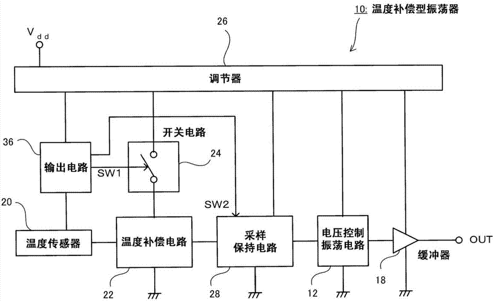
Fig. 1 illustrates the entire block diagram of the temperature compensating type oscillator of this execution mode.The temperature compensating type oscillator 10 of this execution mode has; Be connected with the structure of temperature sensor 20, temperature-compensation circuit 22, sampling hold circuit 28, voltage control oscillating circuit 12, buffer 18 in turn with the mode of series connection; And have adjuster (fixed voltage output circuit) 26, adjuster 26 is used for supplying with fixing voltage (electrical power) to the civilian described output circuit 36 in above-mentioned structural element and back.And; Between adjuster 26 and temperature-compensation circuit 22, be connected with switching circuit 24, and possess the output circuit 36 of exporting the second conducting cut-off signal (SW2) to the switching circuit 24 output first conducting cut-off signals (SW1) and to sampling hold circuit 28.
In addition; The conducting cut-off signal is of back literary composition, is meant the switch-over control signal of the switching of conducting and disconnection between the input and output of switching and sampling hold circuit 28 of the conducting that is respectively applied between the input and output of carrying out switching circuit 24 continuously repeatedly and disconnection.
Fig. 2 illustrates the circuit diagram of the related voltage control oscillating circuit of this execution mode 12.Voltage control oscillating circuit 12 for example is a Kao Bizi type oscillating circuit, and for being the oscillating circuit of oscillation source with piezoelectric vibrator 14.Piezoelectric vibrator 14 can adopt thickness shear oscillator or the tuning fork type vibrator that is for example formed by crystal.And, through applying alternating voltage, thereby can come outputting oscillation signal with predetermined resonance frequency (frequency of oscillation) to piezoelectric vibrator 14.In addition, the variable capacitance diode 16 that becomes variable capacitance is installed in voltage control oscillating circuit 12.Voltage controlled oscillation circuit 12 changes through making the voltage (temperature-compensated voltage) that is applied on the variable capacitance diode 16; Thereby the electric capacity of variable capacitance diode 16 is changed, and then the frequency of oscillation of oscillator signal is changed through this capacitance variations.In addition, buffer 18 is the great circuit of input impedance, its can be only with by the voltage transmission of the oscillator signal of voltage control oscillating circuit 12 outputs to equipment side as linking objective.Thus, voltage control oscillating circuit 12 can be under the condition of the influence of the equipment that does not receive linking objective outputting oscillation signal.
Because the resonance frequency of piezoelectric vibrator 14 changes according to variations in temperature, therefore, the frequency of oscillation of oscillator signal reflects the temperature characterisitic of the resonance frequency of piezoelectric vibrator 14, thereby can change according to variations in temperature.Therefore; Owing on variable capacitance diode 16, be applied with the temperature characterisitic that is used to offset this piezoelectric vibrator 14 temperature-compensated voltage of (amplitude of fluctuation of the frequency of oscillation that will produce owing to the influence of the temperature characterisitic of piezoelectric vibrator 14 suppresses lessly); Therefore the frequency of oscillation of oscillator signal becomes, with the temperature characterisitic that the frequency departure amplitude has been compensated less than the mode of the temperature characterisitic of piezoelectric vibrator 14.
As shown in Figure 1, temperature sensor 20 does, will export the parts of temperature-compensation circuit 22 with the corresponding detected temperatures voltage of the temperature of being measured (temperature detection signal) to, and it is formed by diode etc.When coming formation temperature transducer 20 by diode, make forward current flow through diode, and will be according to temperature and export temperature-compensation circuit 22 to the detected temperatures voltage (V0) that the form of linear function reduces.
Temperature-compensation circuit 22 is to be transfused to detected temperatures voltage from temperature sensor 20, and will to export the parts of sampling hold circuit 28 with the corresponding temperature-compensated voltage of this voltage to.If the piezoelectric vibrator in this execution mode 14 is a tuning fork type vibrator, then the temperature characterisitic of its resonance frequency is described with the curve of quadratic function; If be the thickness shear oscillator, then describe with the curve of cubic function.Thus, in the temperature-compensation circuit 22 there be input in advance, be used for that temperature characterisitic to the resonance frequency of piezoelectric vibrator 14 is similar to, for example zero degree, once, the information of secondary, three inferior temperatures coefficient.Thus; The information of temperature is made as variable; Temperature-compensation circuit 22 is through to calculating the exponent number of above-mentioned these temperatures coefficient as coefficient; Thereby based on the information of the resonance frequency of piezoelectric vibrator 14 under the temperature that is determined and calculate temperature-compensated voltage, and export sampling hold circuit 28 to.
Switching circuit 24 is to be connected between adjuster 26 and the temperature-compensation circuit 22, and to be used to implement temperature-compensation circuit 22 is broken off the parts of control from the conducting of the electrical power of adjuster 26 acceptance.In switching circuit 24; From the output circuit 36 inputs first conducting cut-off signal (SW1); Thereby implement control is broken off in the conducting of temperature-compensation circuit 22; And switching circuit 24 becomes conducting state (on-state) when the voltage of the first conducting cut-off signal (SW1) is H (being in a ratio of high voltage with fiducial value), and when the voltage of the first conducting cut-off signal (SW1) was L (being in a ratio of low-voltage with fiducial value), switching circuit 24 became off-state (non-on-state).
Illustrate the circuit diagram of the related sampling hold circuit of first execution mode among Fig. 3.Sampling hold circuit 28 does; Between following state, carry out the parts of switching controls; That is, be connected with temperature-compensation circuit 22 and at the state (directly output state) that keeps exporting to voltage control oscillating circuit 12 in the temperature-compensated voltage of temperature-compensation circuit 22 outputs, with temperature-compensated voltage; And being connected between cut-out and the temperature-compensation circuit 22, and the temperature-compensated voltage that is kept exported to the state (sampling keeps (S/H) output state) of voltage control oscillating circuit 12.
Sampling hold circuit 28 is made up of switch 30, capacitor 32, buffer 34, is connected with the input of buffer 34 at the outlet side of switch 30, between the input of buffer 34 and ground connection, is connected with capacitor 32.Switch 30 carries out switching controls through the second conducting cut-off signal of supplying with from output circuit 36 (SW2).Particularly; Switch 30 becomes conducting state (on-state) when the voltage of the second conducting cut-off signal (SW2) is H (being in a ratio of high voltage with fiducial value), when the voltage of the second conducting cut-off signal (SW2) is L (being in a ratio of low-voltage with fiducial value), become off-state (non-on-state).Thus, sampling hold circuit 28 is direct output state when conducting state, when off-state, becomes sampling and keeps (S/H) output state.
Fig. 4 illustrates the block diagram of the related output circuit of first execution mode.Output circuit 36 does, generates the circuit of the first conducting cut-off signal (SW1), the second conducting cut-off signal (SW2), its by signal generating circuit 38, cut off circuit 54, start-up circuit 84, branch circuit 68 etc. and constitute.
Signal generating circuit 38 is following circuit; Promptly; When the amplitude of variation (size of voltage variety) of the detected temperatures voltage of importing from temperature sensor 20 (V0) surpasses fixed value; Output voltage is the signal (V1) of H (being in a ratio of high voltage with fiducial value), and when not surpassing, output voltage is the signal (V1) of L (being in a ratio of low-voltage with fiducial value).
Cutting off circuit 54 is following circuit, that is, when the detected temperatures voltage of importing from temperature sensor 20 (V0) was in certain scope, output voltage was the signal (V2) of L, and in the time of beyond being in scope, output voltage is the parts of the signal of H.That is, cut off circuit 54 and be set to, when the temperature that is determined from temperature sensor 20 was in required temperature range, output voltage was the signal (V2) of L, and in the time of beyond being in temperature range, output voltage is the signal of H.
Start-up circuit 84 is following circuit, that is, when the temperature compensating type oscillator 10 that has started this execution mode (for example adjuster 26), during the set time in output voltage be the signal (V3) of H, and output voltage is the signal (V3) of L afterwards.
Be that output becomes from the signal (V1) of signal generating circuit 38 output and circuit from the signal of separating with computing (V4) of the signal (V2) that cuts off circuit 54 outputs with computing (AND) circuit 86.
Exclusive disjunction (OR) circuit 88 does, output become from the signal (V4) of computing circuit 86 outputs circuit with the signal of separating from the exclusive disjunction of the signal (V3) of start-up circuit 84 outputs (V5).
Branch circuit 68 is following circuit; Promptly; When the signal (V5) by 88 outputs of exclusive disjunction circuit is voltage H; Output becomes the first conducting cut-off signal (SW1) and the second conducting cut-off signal (SW2) of voltage H, and on the contrary when signal (V5) is voltage L, exports the first conducting cut-off signal (SW1) and the second conducting cut-off signal (SW2) that become voltage L.
Thus, start the temperature compensating type oscillator 10 of this execution mode and to through in during till the certain hour, because signal (V3) is voltage H, so signal (V5) is voltage H.And regardless of signal (V1), signal (V2), signal (V4), the first conducting cut-off signal (SW1), the second conducting cut-off signal (SW2) exported from branch circuit 68 are voltage H.Thus; Owing to accept voltage is that the switching circuit 24 of the first conducting cut-off signal (SW1) of H becomes conducting state; Therefore temperature-compensation circuit 22 is accepted the electrical power of self tuning regulator 26 and is driven, and to accept voltage be that the sampling hold circuit 28 of the second conducting cut-off signal (SW2) of H becomes direct output state.So; During the certain hour during from startup; Through temperature-compensation circuit 22 is driven; Thereby can be to voltage control oscillating circuit 12 output temperature bucking voltages when starting, implementing the temperature-compensating of oscillator signal, and can in sampling hold circuit 28, keep the temperature-compensated voltage exported from temperature-compensation circuit 22.
And through behind the certain hour, signal (V3) becomes voltage L.But because if signal (V1), signal (V2) are voltage H, and then signal (V4) will become voltage H, so signal (V5) becomes voltage H, thereby the first conducting cut-off signal (SW1), the second conducting cut-off signal (V2) become voltage H.On the other hand; Because when a certain at least side's in signal (V1), the signal (V2) signal is voltage L; Signal (V4) will become voltage L, so signal (V5) also becomes voltage L, thereby the first conducting cut-off signal (SW1), the second conducting cut-off signal (V2) become voltage L.
Promptly; When the temperature of using temperature sensor 20 to determine had surpassed the variable quantity (reference voltage) by signal generating circuit 38 settings for the time variation amount (size of the voltage variety of detected temperatures voltage) with the temperature cutting off that circuit 54 has exported that voltage L carries out beyond the range of set temperature as condition and determine with temperature sensor 20, signal (V5) became voltage H.On the other hand, when the condition that becomes in addition, signal (V5) becomes voltage L.
Illustrate the circuit diagram of the related signal generating circuit of this execution mode among Fig. 5.As shown in Figure 5, signal generating circuit 38 has: low pass filter 40, differential amplifier circuit 46, absolute value circuit 47, comparator 48, voltage control unit.Low pass filter 40 does, the parts that for example formed by the series circuit of resistance 42 and capacitor 44.And, when being transfused to detected temperatures voltage (V0) in this series circuit, the potential difference of the voltage at the two ends that are applied in capacitor 44 is exported as signal (Va).Have from the signal (Va) of low pass filter 40 output, according to the corresponding time constant of the electric capacity of capacitor 44, postponed the voltage of certain hour with respect to the change in voltage of detected temperatures voltage (V0).
Differential amplifier circuit 46 is that the circuit of differential amplifying signal (Vb) has been carried out in output to detected temperatures voltage (V0) and signal (Va).At this, detected temperatures voltage (V0), signal (Va), signal (Vb) have following relation.
Mathematical expression 1
Therefore; Signal (Vb) does; To as the current detected temperatures voltage (V0) of real time temperature information, and scheduled time of current time before detected temperatures voltage (Va) between difference calculate and the value that obtains, its voltage variety with detected temperatures voltage (V0) is corresponding.In addition, on the output of differential amplifier circuit 46, be connected with absolute value circuit 47, thereby output is as the voltage of the absolute value of the output voltage of differential amplifier circuit 46.Therefore, absolute value circuit 47 output has and the signal of the big or small corresponding voltage of the voltage variety of detected temperatures voltage (V0) (Vb ').
Comparator 48 does, is used to export expression signal (Vb ') and as the parts of the signal (V1) of the magnitude relationship between the threshold voltage (Vth) of reference voltage.Therefore, the voltage variety of threshold voltage (Vth) and the detected temperatures voltage (V0) that is set in advance is big or small corresponding.Comparator 48 at Vb ' when being higher than the voltage of Vth, the signal of output voltage H (V1), and at Vb ' when being lower than the voltage of Vth, the signal of output voltage L (V1).
Voltage control unit does, to the parts that threshold voltage vt h controls, for example (Programmable Read Only Memory: programmable read only memory) 50 constitute with control power supply 52 by PROM for it.
The a plurality of discrete magnitudes of voltage of control power supply 52 usefulness come set threshold voltage Vth, and each magnitude of voltage quilt is corresponding with the data in being stored in PROM50.Thus, control power supply 52 can export the threshold voltage vt h of the corresponding magnitude of voltage of data that becomes and from PROM50, read to comparator 48.Thus, voltage control unit is through changing the data that are stored among the PROM50, thereby can regulate the value of the threshold voltage vt h of control power supply 52 outputs.
Therefore, with threshold voltage vt h set low more (height), then signal generating circuit 38 more can responsive (blunt) thus variations in temperature is produced the reaction output voltage is the signal (V1) of H.In addition, through changing the electric capacity of capacitor 44, thus time of delay that can conditioning signal (Va).
Illustrate the circuit diagram of the related cut-out circuit of this execution mode among Fig. 6.As shown in Figure 6, cut off circuit 54 by comparator 56, comparator 58, constitute with computing (AND) circuit 60, inverse (NOT) circuit 62, voltage control unit.
Comparator 56 is the parts of the signal of the magnitude relationship between output expression detected temperatures voltage (V0) and the first threshold voltage (Vth1).Comparator 56 is output voltage H when being higher than the voltage of Vth1 at V0, and is output voltage L when being lower than the voltage of Vth1 at V0.
Comparator 58 is the parts of the signal of the magnitude relationship between output expression detected temperatures voltage (V0) and second threshold voltage (Vth2).Comparator 58 is output voltage L when being higher than the voltage of Vth2 at V0, and is output voltage H when being lower than the voltage of Vth2 at V0.
In addition, with the signal of separating with computing of the output of the output of computing circuit 60 output becoming comparator 56 and comparator 58, inverse circuit 62 is exported the signal (V2) that will reverse with the output of computing circuit 60 and obtain.
Voltage control unit is with mentioned above identical, is made up of with control power supply 66 (Vth1, Vth2) PROM64, and is set to Vth2 and is higher than Vth1.
Thus, when detected temperatures voltage (V0) is Vth1 when following, the signal of comparator 56 output voltage L, the signal of comparator 58 output voltage H.Thus since with the signal of computing circuit 60 output voltage L, so the signal (V2) of inverse circuit 62 outputs becomes voltage H.Equally, when detected temperatures voltage (V0) is Vth2 when above, the signal of comparator 56 output voltage H, the signal of comparator 58 output voltage L.Thus since with the signal of computing circuit 60 output voltage L, so the signal (V2) of inverse circuit 62 outputs becomes voltage H.
On the other hand, when detected temperatures voltage (V0) is between Vth1 and Vth2, the signal of comparator 56 output voltage H, the signal of comparator 58 output voltage H.Thus since with the signal of computing circuit 60 output voltage H, so the signal (V2) of inverse circuit 62 outputs becomes voltage L.
In the frequency-temperature characteristic of piezoelectric vibrator 14; Existence with respect to variations in temperature and the minimum zone of frequency change (near the temperature range the extreme value of the curve of frequency-temperature characteristic and this extreme value, promptly therebetween the amplitude of variation of frequency-temperature characteristic in the stability of temperature compensating type oscillator 10 desired frequency-temperature characteristics with interior zone).Thus, owing in the said temperature scope, need not to carry out the renewal of temperature-compensated voltage, therefore need not to carry out the driving of temperature-compensation circuit.In addition, as stated, temperature sensor 20 has the tendency that detected temperatures voltage (V0) reduces with the form dullness of linear function along with the temperature rising.Therefore, in this execution mode, first threshold voltage (Vth1) is set at the corresponding voltage of temperature with the upper limit of said temperature scope, second threshold voltage (Vth2) is set at the corresponding voltage of temperature with the lower limit of said temperature scope.Through setting Vth1 like this, Vth2; Thereby the detected temperatures voltage (V0) of temperature sensor 20 output with the scope of the above-mentioned corresponding voltage of temperature range in the time; Cut off circuit 54 through the signal (V1) of signal generating circuit being cut off, thereby can stop supply to the electrical power of temperature-compensation circuit 22 with computing circuit 86.Thus, can significantly reduce the electric power consumption of temperature-compensation circuit 22.
In the temperature compensating type oscillator 10 of this execution mode, consume the electric current of about 1mA on the whole altogether.Wherein, consume 1/3rd of whole electric currents in the temperature-compensation circuit 22, consume 1/3rd in the voltage control oscillating circuit 12, consume 1/3rd in the buffer 18.Therefore, through shortening the driving time of temperature-compensation circuit 22, thereby can reduce the whole electric power consumption of temperature compensating type oscillator 10.In addition, though this execution mode owing to used output circuit 36 thereby increased electric power consumption, because the electric current that uses is approximately tens μ A degree, so can not impact the electric power consumption of the integral body of temperature compensating type oscillator 10.
But in the temperature compensating type oscillator 10 of this execution mode, temperature-compensation circuit 22 needs the scheduled time from being dropped into by switching circuit 24 till electrical power play stably the output temperature bucking voltage.Therefore, when under the temperature-compensated voltage unsure state, when the switch 30 in the sampling hold circuit 28 is connected, will export unsettled temperature-compensated voltage to voltage control oscillating circuit 12, thereby oscillator signal might be unstable.
In addition; Because when output from the temperature-compensated voltage of temperature-compensation circuit 22 is stopped; Capacitor 32 in the temperature holding circuit 28 will discharge, and therefore be difficult to the temperature-compensated voltage that keeps correct.Therefore; The following mode of preferred employing in this execution mode; That is, after temperature-compensation circuit 22 is opened and passed through the scheduled time, the switch 30 of sampling hold circuit 28 is connected; And after the switch in sampling hold circuit 28 30 is cut off, stop to supply with electrical power to temperature-compensation circuit 22.
Therefore; In this execution mode; In order to connect and to remove connection according to said sequence; Illustrated branch circuit 68 below the use, and to the first conducting cut-off signal (SW1) that exports switching circuit 24 to, and export between the second conducting cut-off signal (SW2) of sampling hold circuit 28 and give the time difference.Promptly; Correct time that Continuity signal produced of the first conducting cut-off signal (SW1), and correct time that Continuity signal produced of the second conducting cut-off signal (SW2) between give the time difference; In addition, correct time that cut-off signal produced of the first conducting cut-off signal (SW1), and correct time that cut-off signal produced of the second conducting cut-off signal (SW2) between give the time difference.
Illustrate the circuit diagram and the sequential chart of the related branch circuit of first execution mode among Fig. 7.In Fig. 7, the sequential chart of (for example, variations in temperature situation about increasing and situation about reducing repeatedly alternately time) when having put down in writing signal (V5) repeatedly alternately for voltage H, voltage L.As shown in Figure 7, branch circuit 68 is by delay circuit 70, exclusive disjunction circuit 80, constitute with computing circuit 82.Delay circuit 70 does, has been connected buffer 76, buffer 78 with the parts as inverter at the input side and the outlet side of the low pass filter that is made up of resistance 72 (R) and capacitor 74 (C).At this, when signal (V5) was voltage L, buffer 76 was output as voltage H, thereby capacitor 74 is recharged, and the output of buffer 78, was that inhibit signal (Vd) becomes voltage L.In addition, when signal (V5) was voltage H, buffer 76 was output as voltage L, thereby capacitor 74 is discharged, and the output of buffer 78, was that inhibit signal (Vd) becomes voltage H.
Next, when signal (V5) when voltage L rises to voltage H, capacitor 74 bases are discharged with the corresponding time constant of the electric capacity of capacitor 74, thus the voltage that is applied on the capacitor 74 converges to low-voltage (zero) along with effluxion.Thus, inhibit signal (Vd) converges to voltage H from voltage L with the form of delay scheduled time.In addition, when signal (V5) when voltage H drops to voltage L, capacitor 74 charges according to said time constant, thus the voltage that is applied on the capacitor 74 is converged to predetermined voltage.Thus, inhibit signal (Vd) converges to voltage L from voltage H with the form that has postponed the scheduled time.
Exclusive disjunction circuit 80 does, will become signal that signal (V5) and the exclusive disjunction of inhibit signal (Vd) separate exports switching circuit 24 to as the first conducting cut-off signal (SW1) parts.Exclusive disjunction circuit 80 does, the voltage L of signal (V5) is identified as voltage L, and the voltage H of signal (V5) is identified as the parts of voltage H.On the other hand; Exclusive disjunction circuit 80 is adjusted to; When the voltage of inhibit signal (Vd) surpassed voltage H and the voltage Vm between the voltage L of inhibit signal (Vd), during for example for the voltage Vm of (voltage H+ voltage L)/2; (Vd) is identified as voltage H with inhibit signal, and when the voltage of inhibit signal (Vd) was lower than Vm, (Vd) was identified as voltage L with inhibit signal.
When exclusive disjunction circuit 80 was identified as voltage H at the signal with a certain side in signal (V5) and the inhibit signal (Vd), output voltage was the first conducting cut-off signal (SW1) of H.Thus, when signal (V5) when voltage L rises to voltage H because exclusive disjunction circuit 80 is when signal (V5) rises to voltage H, (V5) is identified as voltage H with signal, can output voltage be the first conducting cut-off signal (SW1) of H therefore.
On the other hand, when signal (V5) when voltage H drops to voltage L, exclusive disjunction circuit 80 is when signal (V5) drops to voltage L, (V5) is identified as voltage L with signal.But, since exclusive disjunction circuit 80 till the voltage of inhibit signal (Vd) reaches Vm below during in, (Vd) is identified as voltage H with inhibit signal, therefore, with continue exporting the first conducting cut-off signal (SW1) that becomes voltage H.And exclusive disjunction circuit 80 is after inhibit signal (Vd) reaches below the voltage Vm, and (Vd) is identified as voltage L with inhibit signal, thereby can export the first conducting cut-off signal (SW1) that becomes voltage L.
Be that the signal of separating with computing that will become signal (V5) and inhibit signal (Vd) exports the parts of sampling hold circuit 28 to as the second conducting cut-off signal (SW2) with computing circuit 82.Be the voltage L of signal (V5) to be identified as voltage L, and the voltage H of signal (V5) is identified as the parts of voltage H with computing circuit 82.On the other hand; Be adjusted to computing circuit 82; When the voltage of inhibit signal (Vd) surpassed voltage H and the voltage Vm between the voltage L of inhibit signal (Vd), during for example for the voltage Vm of (voltage H+ voltage L)/2; (Vd) is identified as voltage H with inhibit signal, and when the voltage of inhibit signal (Vd) was lower than Vm, (Vd) was identified as voltage L with inhibit signal.
With computing circuit 82 when the signal with a certain side in signal (V5) and the inhibit signal (Vd) is identified as voltage H, output becomes the second conducting cut-off signal (SW2) of voltage H.Thus, when signal (V5) when voltage L rises to voltage H, with computing circuit 82 when signal (V5) rises to voltage H, (V5) is identified as voltage H with signal.But, since with computing circuit 82 till the voltage of inhibit signal (Vd) reaches Vm more than during in, therefore (Vd) is identified as voltage L with inhibit signal, exports the first conducting cut-off signal (SW1) that becomes voltage L.And, with computing circuit 82 after the voltage of inhibit signal (Vd) becomes more than the Vm, (Vd) is identified as voltage H with inhibit signal, thereby can export the second conducting cut-off signal (SW2) that becomes voltage H.
On the other hand; When signal (V5) when voltage H drops to voltage L; Since with computing circuit 82 when signal (V5) drops to voltage L; (V5) is identified as voltage L with signal, and therefore regardless of the voltage of inhibit signal (Vd), all output becomes the second conducting cut-off signal (SW2) of voltage L.
Through implementing aforesaid control; Thereby the first conducting cut-off signal of exporting from branch circuit 68 (SW1), the second conducting cut-off signal (SW2); The first conducting cut-off signal (SW1) rises prior to the second conducting cut-off signal (SW2), and is later than the second conducting cut-off signal (SW2) and descends.In addition, through the value of Vm, the electric capacity of capacitor 58 are changed, thereby can regulate the first conducting cut-off signal (SW1) and the rising of the second conducting cut-off signal (SW2), the time difference of decline.
Therefore; The switching circuit of being controlled by the first conducting cut-off signal (SW1) 24, promptly carry out the temperature-compensation circuit 22 that control is broken off in conducting by switching circuit 24; Can, the sampling hold circuit of being controlled by the second conducting cut-off signal (SW2) 28 become conducting state before becoming the certain hour in correct time of direct output state.And temperature-compensation circuit 22 can reach sampling at sampling hold circuit 28 and keep becoming off-state after (S/H) output state.
Illustrate the circuit diagram of the change example of the said signal generating circuit that relates to of this execution mode among Fig. 8.As the change of signal generating circuit 38 example, can replace low pass filter 40 and use the frequency divider 90 and second sampling hold circuit 92 as timer.
Frequency divider 90 does, will carry out frequency division to the oscillator signal of voltage control oscillating circuit 12 and parts that the impulse wave that obtains is exported as drive signal.Drive signal does, repeats to become the signal of state of state and the voltage L of voltage H, and is sufficiently short but the duration of voltage H was compared with the duration of voltage L.
Second sampling hold circuit 92 is same with sampling hold circuit 28, is made up of switch 94, capacitor 96, buffer 98.And; Second sampling hold circuit 92 does; Acceptance is from the drive signal of frequency divider 90; Thereby the parts that can between following state, switch, that is, and being connected when keeping detected temperatures voltage (Va), the state (directly output state) of output detected temperatures voltage (V0) with temperature sensor 20; Cut off with temperature sensor 20 between the state that is connected and export the detected temperatures voltage (Va) that is kept (the maintenance output state of sampling).
Second sampling hold circuit 92 becomes direct output state when accepting the drive signal of voltage H, when accepting the drive signal of voltage L, become sampling and keep output state.And when second sampling hold circuit 92 was in direct output state, detected temperatures voltage (V0) was consistent with the detected temperatures voltage (Va) that is kept.On the other hand; When second sampling hold circuit 92 is in sampling maintenance output state and has variations in temperature; To next voltage be till the drive signal of H arrives during in, the difference between detected temperatures voltage (V0) and the detected temperatures voltage (Vc) that kept increases gradually.Therefore, be connected the variable quantity that differential amplifier circuit 46 on second sampling hold circuit 92 can go out detected temperatures voltage (V0) in the computation of Period of each drive signal.And, thereby because frequency divider 90 can be selected the cycle through setting is changed, therefore, can at random regulate the counting period of 46 pairs of variations in temperature of differential amplifier circuit corresponding to the cycle of frequency divider.
Illustrate the change example of the related temperature compensating type oscillator of this execution mode among Fig. 9; Wherein, Fig. 9 (a) is for having disposed the figure of low pass filter between temperature-compensation circuit and sampling hold circuit, Fig. 9 (b) is for having disposed the figure of low pass filter between sampling hold circuit and voltage control oscillating circuit.
It is identical with first execution mode basically to change the related temperature compensating type oscillator 100 of example; But it is different on following point; That is, between temperature-compensation circuit 22 and sampling hold circuit 28 or at least one side's between sampling hold circuit 28 and the voltage control oscillating circuit 12 position dispose second low pass filter 102.Second low pass filter 102 has the structure same with low pass filter 40.And; Though second low pass filter can application drawing 9 (a), any one mode among Fig. 9 (b); But, through be configured in the back segment of sampling hold circuit 28 with the mode shown in Fig. 9 (b), the electrical noise that is produced in the time of can reducing the switching controls of sampling hold circuit 28.
The time of the temperature-compensated voltage of the temperature compensating type oscillator that the temperature compensating type oscillator that illustrates first execution mode among Figure 10 is related with changing example is interdependent.In Figure 10, dullness increases because the temperature on every side of temperature compensating type oscillator 10,100 is along with effluxion, therefore wants the situation of account temperature bucking voltage dull increase along with effluxion.In the first embodiment, after just temperature-compensation circuit 22 being made as conducting state, sampling hold circuit 28 will switch to the temperature-compensated voltage by temperature-compensation circuit 22 new inputs from the temperature-compensated voltage that is kept.Thus, when carrying out this switching, temperature-compensated voltage on time orientation with discontinuous, thereby might cause negative effect to voltage control oscillating circuit 12.Therefore, through disposing second low pass filter 102, thereby become gently the time of the temperature-compensated voltage of new input, and then alleviate burden voltage control oscillating circuit 12 with the mode of temperature compensating type oscillator 100 that changes example.In addition, the reason that temperature-compensated voltage can reduce when sampling hold circuit 28 keeps (S/H) output state for sampling is that the capacitor 30 in the sampling hold circuit 28 is emitted electric charge.
In addition, in any one execution mode, the time compole from the unlatching of temperature-compensation circuit 22 time till stable is short, and under the enough big situation of the capacity of the capacitor 32 of sampling hold circuit 28, does not all need above-mentioned branch circuit 68.And, in any one execution mode, all can construct the electronic equipment that can carry on gps receiver and mobile phone etc. and can when keeping high-precision temperature-compensating, realize economize on electricityization.In addition; In the piezoelectric vibrator that in voltage control circuit, is adopted, when the curve of frequency-temperature characteristic has a plurality of extreme value, only need to adopt following mode to get final product; Promptly; To comprising which extreme value in the serviceability temperature scope, and implementing the rewriting to the data of PROM64, is to be used for exporting corresponding to serviceability temperature cutting off the first threshold voltage and second threshold voltage that circuit 54 is used to the rewriting of the data of PROM64.
Symbol description
10: the temperature compensating type oscillator; 12: voltage control oscillating circuit; 14: piezoelectric vibrator; 16: variable capacitance diode; 18: buffer; 20: temperature sensor; 22: temperature-compensation circuit; 24: switching circuit; 26: adjuster; 28: sampling hold circuit; 30: switch; 32: capacitor; 34: buffer; 36: output circuit; 38: signal generating circuit; 40: low pass filter; 42: resistance; 44: capacitor; 46: differential amplifier circuit; 47: absolute value circuit; 48: comparator; 50:PROM; 52: the control power supply; 54: cut off circuit; 56: comparator; 58: comparator; 60: with computing circuit; 62: the inverse circuit; 64:PROM; 66: the control power supply; 68: branch circuit; 70: delay circuit; 72: resistance; 74: capacitor; 76: buffer; 78: buffer; 80: the exclusive disjunction circuit; 82: with computing circuit; 84: start-up circuit; 86: with computing circuit; 88: the exclusive disjunction circuit; 90: frequency divider; 92: the second sampling hold circuits; 94: switch; 96: capacitor; 98: buffer; 100: the temperature compensating type oscillator; 102: the second low pass filters; 200: the temperature compensating type oscillator; 202: oscillating circuit; 204: quartz crystal; 206: temperature-compensation circuit; 208: temperature sensor.