CN103179357A - Solid-state imaging apparatus, method of manufacturing solid-state imaging apparatus and electronic device - Google Patents
Solid-state imaging apparatus, method of manufacturing solid-state imaging apparatus and electronic device Download PDFInfo
- Publication number
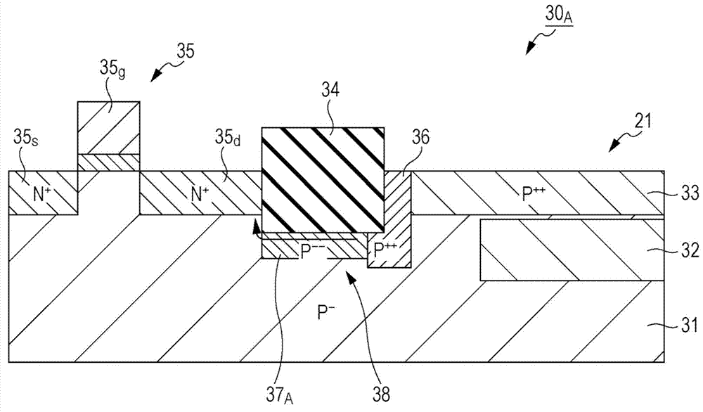
- CN103179357A CN103179357A CN2012105208609A CN201210520860A CN103179357A CN 103179357 A CN103179357 A CN 103179357A CN 2012105208609 A CN2012105208609 A CN 2012105208609A CN 201210520860 A CN201210520860 A CN 201210520860A CN 103179357 A CN103179357 A CN 103179357A
- Authority
- CN
- China
- Prior art keywords
- region
- element isolation
- unit
- isolation unit
- state imaging
- Prior art date
- Legal status (The legal status is an assumption and is not a legal conclusion. Google has not performed a legal analysis and makes no representation as to the accuracy of the status listed.)
- Pending
Links
Images


Classifications
-
- H—ELECTRICITY
- H10—SEMICONDUCTOR DEVICES; ELECTRIC SOLID-STATE DEVICES NOT OTHERWISE PROVIDED FOR
- H10F—INORGANIC SEMICONDUCTOR DEVICES SENSITIVE TO INFRARED RADIATION, LIGHT, ELECTROMAGNETIC RADIATION OF SHORTER WAVELENGTH OR CORPUSCULAR RADIATION
- H10F77/00—Constructional details of devices covered by this subclass
-
- H—ELECTRICITY
- H10—SEMICONDUCTOR DEVICES; ELECTRIC SOLID-STATE DEVICES NOT OTHERWISE PROVIDED FOR
- H10F—INORGANIC SEMICONDUCTOR DEVICES SENSITIVE TO INFRARED RADIATION, LIGHT, ELECTROMAGNETIC RADIATION OF SHORTER WAVELENGTH OR CORPUSCULAR RADIATION
- H10F39/00—Integrated devices, or assemblies of multiple devices, comprising at least one element covered by group H10F30/00, e.g. radiation detectors comprising photodiode arrays
- H10F39/011—Manufacture or treatment of image sensors covered by group H10F39/12
- H10F39/014—Manufacture or treatment of image sensors covered by group H10F39/12 of CMOS image sensors
-
- H—ELECTRICITY
- H10—SEMICONDUCTOR DEVICES; ELECTRIC SOLID-STATE DEVICES NOT OTHERWISE PROVIDED FOR
- H10F—INORGANIC SEMICONDUCTOR DEVICES SENSITIVE TO INFRARED RADIATION, LIGHT, ELECTROMAGNETIC RADIATION OF SHORTER WAVELENGTH OR CORPUSCULAR RADIATION
- H10F39/00—Integrated devices, or assemblies of multiple devices, comprising at least one element covered by group H10F30/00, e.g. radiation detectors comprising photodiode arrays
- H10F39/80—Constructional details of image sensors
- H10F39/807—Pixel isolation structures
-
- H—ELECTRICITY
- H10—SEMICONDUCTOR DEVICES; ELECTRIC SOLID-STATE DEVICES NOT OTHERWISE PROVIDED FOR
- H10F—INORGANIC SEMICONDUCTOR DEVICES SENSITIVE TO INFRARED RADIATION, LIGHT, ELECTROMAGNETIC RADIATION OF SHORTER WAVELENGTH OR CORPUSCULAR RADIATION
- H10F71/00—Manufacture or treatment of devices covered by this subclass
-
- H—ELECTRICITY
- H10—SEMICONDUCTOR DEVICES; ELECTRIC SOLID-STATE DEVICES NOT OTHERWISE PROVIDED FOR
- H10F—INORGANIC SEMICONDUCTOR DEVICES SENSITIVE TO INFRARED RADIATION, LIGHT, ELECTROMAGNETIC RADIATION OF SHORTER WAVELENGTH OR CORPUSCULAR RADIATION
- H10F39/00—Integrated devices, or assemblies of multiple devices, comprising at least one element covered by group H10F30/00, e.g. radiation detectors comprising photodiode arrays
- H10F39/10—Integrated devices
- H10F39/12—Image sensors
- H10F39/18—Complementary metal-oxide-semiconductor [CMOS] image sensors; Photodiode array image sensors
Landscapes
- Solid State Image Pick-Up Elements (AREA)
- Engineering & Computer Science (AREA)
- Manufacturing & Machinery (AREA)
- Element Separation (AREA)
Abstract
本发明提供了一种固态摄像装置、固态摄像装置的制造方法以及电子装置,所述固态摄像装置包括:多个光电转换单元;元件隔离单元,其在所述多个光电转换单元之间进行元件隔离;以及扩散阻止单元,其用于阻止在所述元件隔离单元的界面上生成的暗电流成分扩散到围绕所述暗电流成分的生成区的区域。根据本发明,由于阻止了在元件隔离单元的界面上生成的暗电流成分向周围区域的扩散,可以进一步可靠地抑制暗电流成分对光电转换单元的负面影响。
The present invention provides a solid-state imaging device, a manufacturing method of the solid-state imaging device, and an electronic device. The solid-state imaging device includes: a plurality of photoelectric conversion units; isolation; and a diffusion preventing unit for preventing a dark current component generated on an interface of the element isolation unit from diffusing to a region surrounding a generation region of the dark current component. According to the present invention, since the dark current component generated on the interface of the element isolation unit is prevented from diffusing to the surrounding area, the negative influence of the dark current component on the photoelectric conversion unit can be further reliably suppressed.
Description
相关申请的交叉引用Cross References to Related Applications
本发明包含与2011年12月20日向日本专利局提交的日本优先权专利申请第2011-277990号相关的主题,其全部内容通过引用结合于此。The present application contains subject matter related to Japanese Priority Patent Application No. 2011-277990 filed in the Japan Patent Office on Dec. 20, 2011, the entire content of which is hereby incorporated by reference.
技术领域technical field
本发明涉及一种固态摄像装置、固态摄像装置的制造方法以及电子装置。The present invention relates to a solid-state imaging device, a method for manufacturing the solid-state imaging device, and an electronic device.
背景技术Background technique
在固态摄像装置中,获取到的图像的质量取决于暗时的特性。因此,在固态摄像装置中,减少流入光电转换单元中的引起暗电流的微小漏电流是很重要的,这是影响图像质量的重要因素之一。生成漏电流的原因之一是元件隔离单元的界面上生成的电子。一般说来,氧化膜和半导体基板的界面存在一些问题。具体地,由于应力和蚀刻损伤被积累,在元件隔离单元的附近容易出现缺陷,并成为暗电流成分的生成源。In a solid-state imaging device, the quality of an acquired image depends on the characteristics of dark time. Therefore, in a solid-state imaging device, it is important to reduce a minute leak current that flows into a photoelectric conversion unit causing a dark current, which is one of important factors affecting image quality. One of the causes of leakage current is electrons generated at the interface of the element isolation unit. In general, there are some problems at the interface between the oxide film and the semiconductor substrate. Specifically, since stress and etching damage are accumulated, defects tend to occur in the vicinity of element isolation cells, and become a generation source of dark current components.
在相关技术中,为了抑制暗电流成分的生成,提出了一种以高浓度的P型区围绕元件隔离单元附近区域的结构(例如,参见日本未经审查的专利申请公开第2005-123280号和第2007-134639号)。详细地,通过根据相关技术的该结构,通过增加元件隔离单元的界面的P型区的浓度,抑制了暗电流在界面上的生成量。In the related art, in order to suppress the generation of dark current components, a structure in which a region near the element isolation unit is surrounded by a high-concentration P-type region has been proposed (for example, see Japanese Unexamined Patent Application Publication No. 2005-123280 and No. 2007-134639). In detail, with this structure according to the related art, by increasing the concentration of the P-type region of the interface of the element isolation unit, the amount of generation of dark current on the interface is suppressed.
日本未经审查的专利公开第2005-123280号和第2007-134639号中公开的相关技术的任何结构用于抑制在界面上的暗电流成分的生成量。然而,由于抑制暗电流成分的区域是有限制的,暗电流成分的生成量不为零。已生成的暗电流成分向具有相同浓度的区域或比P型区域具有更低浓度(浓度低)的区域扩散。Any structure of the related art disclosed in Japanese Unexamined Patent Publication No. 2005-123280 and No. 2007-134639 serves to suppress the amount of generation of dark current components on the interface. However, since the region where the dark current component is suppressed is limited, the generation amount of the dark current component is not zero. The generated dark current component diffuses to a region having the same concentration or a region having a lower concentration (low density) than the P-type region.
在日本未经审查的专利公开第2005-123280号和第2007-134639号中公开的相关技术的结构的情况下,已生成的电子在生成电子的区域周围的P型区中扩散,一部分已生成的电子流入具有N型正电位的光电转换单元(光电二极管)。图11示出了在日本未经审查的专利公开第2005-123280号中公开的相关技术的结构1的情况下在元件隔离单元的界面上生成的电子的流动,图12示出了在日本未经审查的专利公开第2007-134639号中公开的相关技术的结构2的情况下在元件隔离单元的界面上生成的电子的流动。In the case of the structures of the related art disclosed in Japanese Unexamined Patent Publication No. 2005-123280 and No. 2007-134639, the generated electrons diffuse in the P-type region around the region where the electrons are generated, and a part of the generated The electrons flow into the photoelectric conversion unit (photodiode) with N-type positive potential. FIG. 11 shows the flow of electrons generated on the interface of the element isolation unit in the case of the structure 1 of the related art disclosed in Japanese Unexamined Patent Publication No. 2005-123280, and FIG. The flow of electrons generated on the interface of the element isolation unit in the case of the structure 2 of the related art disclosed in Examined Patent Publication No. 2007-134639.
发明内容Contents of the invention
在本发明中,希望提供一种能够进一步可靠地抑制在元件隔离单元的界面上生成的暗电流成分对光电转换单元的负面影响的固态摄像装置、该固态摄像装置的制造方法以及包括用作摄像单元(图像获取单元)的该固态摄像装置的电子装置。In the present invention, it is desired to provide a solid-state imaging device capable of further reliably suppressing the negative influence of dark current components generated on the interface of the element isolation unit on the photoelectric conversion unit, a manufacturing method of the solid-state imaging device, and an imaging device including an imaging device. The electronic device of the solid-state imaging device of the unit (image acquisition unit).
根据本发明的实施例的固态摄像装置包括:多个光电转换单元;元件隔离单元,其在多个光电转换单元之间进行元件隔离;以及扩散阻止单元,其用于阻止在所述元件隔离单元的界面上生成的暗电流成分扩散到围绕所述暗电流成分的生成区的区域。A solid-state imaging device according to an embodiment of the present invention includes: a plurality of photoelectric conversion units; an element isolation unit that performs element isolation between the plurality of photoelectric conversion units; The dark current component generated on the interface diffuses to the region surrounding the generation region of the dark current component.
根据本发明的实施例的固态摄像装置可以作为摄像单元(图像获取单元)用于诸如具有摄像功能的个人数字助理等电子装置(诸如数码相机、摄像机或移动电话)中。A solid-state imaging device according to an embodiment of the present invention can be used as an imaging unit (image acquisition unit) in electronic devices such as personal digital assistants having an imaging function, such as digital cameras, video cameras, or mobile phones.
在通过元件隔离单元在多个光电转换单元之间进行元件隔离而形成的固态摄像装置中,扩散阻止单元阻止了在元件隔离单元的界面上生成的暗电流向周围区域扩散。如上所述,相较于抑制暗电流成分的生成的相关技术中的结构,即相较于暗电流成分的生成量不为零的相关技术中的结构,无须抑制在元件隔离单元的界面上的暗电流成分的生成,而是通过阻止已生成的暗电流成分向周围区域扩散,可以减少暗电流成分对光电转换单元的影响。In a solid-state imaging device formed by element isolation between a plurality of photoelectric conversion units by an element isolation unit, the diffusion preventing unit prevents dark current generated at an interface of the element isolation unit from spreading to a surrounding area. As described above, compared with the structure in the related art that suppresses the generation of dark current components, that is, compared to the structure in the related art in which the amount of generation of dark current components is not zero, it is not necessary to suppress the The generation of dark current components, but by preventing the generated dark current components from diffusing to the surrounding area, can reduce the influence of dark current components on the photoelectric conversion unit.
根据本发明,由于阻止了在元件隔离单元的界面上生成的暗电流成分向周围区域的扩散,可以进一步可靠地抑制暗电流成分对光电转换单元的负面影响。According to the present invention, since the dark current component generated on the interface of the element isolation unit is prevented from diffusing to the surrounding area, the negative influence of the dark current component on the photoelectric conversion unit can be further reliably suppressed.
附图说明Description of drawings
图1是示意性地示出了应用本发明的实施例的CMOS图像传感器的系统配置的系统配置图;1 is a system configuration diagram schematically showing a system configuration of a CMOS image sensor to which an embodiment of the present invention is applied;
图2是示出了单位像素的电路配置的示例的电路图;2 is a circuit diagram showing an example of a circuit configuration of a unit pixel;
图3是示出了根据示例1的单位像素的主要部分的像素结构的截面图;3 is a cross-sectional view showing a pixel structure of a main part of a unit pixel according to Example 1;
图4是示出了根据示例2的单位像素的主要部分的像素结构的截面图;4 is a cross-sectional view showing a pixel structure of a main part of a unit pixel according to Example 2;
图5是示出了流入相关技术的结构1和2以及示例2的结构的光电二极管的电流量的模拟结果的图;5 is a graph showing simulation results of current amounts flowing into photodiodes of Structures 1 and 2 and the structure of Example 2 of the related art;
图6是示出了第二区域在深度方向上的宽度为5nm、10nm和20nm的情况下,流入示例2的结构的光电二极管的电流量的模拟结果的图;6 is a graph showing simulation results of the amount of current flowing into the photodiode of the structure of Example 2 in the case where the width of the second region in the depth direction is 5 nm, 10 nm, and 20 nm;
图7是示出了根据示例3的单位像素的主要部分的像素结构的截面图;7 is a cross-sectional view showing a pixel structure of a main part of a unit pixel according to Example 3;
图8A和8B是图示了根据示例1和2的像素结构的制造方法的第一示例的制造步骤的步骤截面图;8A and 8B are step sectional views illustrating manufacturing steps of the first example of the manufacturing method of the pixel structure according to Examples 1 and 2;
图9A和9B是图示了根据示例1和2的像素结构的制造方法的第二示例的制造步骤的步骤截面图;9A and 9B are step sectional views illustrating manufacturing steps of the second example of the manufacturing method of the pixel structure according to Examples 1 and 2;
图10A和10B是图示了根据示例3的像素结构的制造方法的制造步骤的步骤截面图;10A and 10B are step sectional views illustrating manufacturing steps of a method of manufacturing a pixel structure according to Example 3;
图11是示出了在相关技术的结构1的情况下在元件隔离绝缘膜的界面上生成的电子的流动的图;11 is a diagram showing the flow of electrons generated on the interface of an element isolation insulating film in the case of Structure 1 of the related art;
图12是示出了在相关技术的结构2的情况下在元件隔离绝缘膜的界面上生成的电子的流动的图;12 is a diagram showing the flow of electrons generated on the interface of an element isolation insulating film in the case of Structure 2 of the related art;
图13是示出了作为本发明的实施例的电子装置的摄像装置的配置示例的框图。FIG. 13 is a block diagram showing a configuration example of an imaging device as an electronic device of an embodiment of the present invention.
具体实施方式Detailed ways
在下文中,将参考附图对实现本发明的技术的实施例(在下文中,称为“实施例”)进行详细描述。本发明不局限于这些实施例,这些实施例的各种数值和材料都仅是示例。在以下描述中,相同组件或具有相同功能的组件使用相同附图标记,将省略重复描述。将按照以下列顺序进行描述:Hereinafter, embodiments (hereinafter, referred to as “embodiments”) for realizing the technology of the present invention will be described in detail with reference to the accompanying drawings. The present invention is not limited to these examples, and various numerical values and materials of these examples are just examples. In the following description, the same components or components having the same function use the same reference numerals, and repeated description will be omitted. It will be described in the following order:
1.关于本发明的固态摄像装置、固态摄像装置的制造方法以及电子装置的概述1. Outline of the solid-state imaging device, the manufacturing method of the solid-state imaging device, and the electronic device of the present invention
2.实施例2. Example
2-1.系统配置2-1. System configuration
2-2.单位像素的电路配置2-2. Circuit configuration of unit pixel
2-3.在元件隔离单元的界面上生成的暗电流成分2-3. Dark current components generated at the interface of element isolation cells
2-4.示例12-4. Example 1
2-5.示例22-5. Example 2
2-6.示例32-6. Example 3
2-7.制造方法2-7. Manufacturing method
3.应用示例3. Application examples
4.电子装置4. Electronic devices
5.本发明的配置5. Configuration of the present invention
1.关于本发明的固态摄像装置、固态摄像装置的制造方法以及电子装置的概述1. Outline of the solid-state imaging device, the manufacturing method of the solid-state imaging device, and the electronic device of the present invention
本发明的固态摄像装置具有包括元件隔离单元的配置,该元件隔离单元在多个光电转换单元之间进行元件隔离。元件隔离单元包括用于将光电转换单元的区域和除了光电转换单元之外的元件区分隔开的侧面。对于元件隔离单元,例如可以使用众所周知的浅沟槽隔离(STI)或硅局部氧化(LOCOS)。The solid-state imaging device of the present invention has a configuration including an element isolation unit that performs element isolation between a plurality of photoelectric conversion units. The element isolation unit includes side surfaces for separating a region of the photoelectric conversion unit from an element region other than the photoelectric conversion unit. For element isolation cells, for example, the well-known shallow trench isolation (STI) or local oxidation of silicon (LOCOS) can be used.
用于在光电转换单元中光电转换的电荷的任何传输方法都可以用于本发明的固态摄像装置中。换言之,本发明的固态摄像装置可以是以电荷耦合器件(CCD)图像传感器为代表的电荷传输型固态摄像装置,或者可以是以互补金属氧化物半导体(CMOS)图像传感器为代表的放大型固态摄像装置。Any transfer method for charges photoelectrically converted in the photoelectric conversion unit can be used in the solid-state imaging device of the present invention. In other words, the solid-state imaging device of the present invention may be a charge-transfer type solid-state imaging device typified by a charge-coupled device (CCD) image sensor, or may be an amplifying solid-state imaging device typified by a complementary metal-oxide-semiconductor (CMOS) image sensor. device.
在包括元件隔离单元的固态摄像装置中,由于应力和蚀刻损伤被积累,元件隔离单元附近区域经常出现问题并成为暗电流成分的生成源。本发明的固态摄像装置包括扩散阻止单元,该扩散阻止单元用于阻止在元件隔离单元的界面上生成的暗电流成分向围绕暗电流成分的生成区的区域扩散。In a solid-state imaging device including an element isolation unit, since stress and etching damage are accumulated, a region near the element isolation unit often has problems and becomes a generation source of dark current components. A solid-state imaging device according to the present invention includes a diffusion preventing unit for preventing dark current components generated on an interface of the element isolation unit from diffusing to a region surrounding the generation region of the dark current components.
最好是至少沿着元件隔离单元的底面形成扩散阻止单元,以阻止在元件隔离单元的至少底面的界面中生成的暗电流成分向周围区域扩散。不仅沿着底面形成扩散阻止单元,可以沿着元件隔离单元的位于光电转换单元侧的侧壁形成扩散阻止单元。因此,可以阻止在光电转换单元侧的侧壁的界面上生成的暗电流成分向光电转换单元侧的区域扩散。It is preferable to form the diffusion preventing means along at least the bottom surface of the element isolation unit to prevent the dark current component generated in the interface of at least the bottom surface of the element isolation unit from diffusing to the surrounding area. Not only is the diffusion preventing unit formed along the bottom surface, but the diffusion preventing unit may be formed along the side wall of the element isolation unit on the side of the photoelectric conversion unit. Therefore, it is possible to prevent the dark current component generated at the interface of the side wall on the side of the photoelectric conversion unit from diffusing to the region on the side of the photoelectric conversion unit.
取代沿着元件隔离单元的在光电转换单元侧的侧壁形成扩散阻止单元的是,也可以采用设置第一导电型的第一区域的配置,该第一导电型的第一区域比光电转换单元周围的第一导电型的阱区具有更高的杂质浓度,以通过第一区域覆盖光电转换单元侧的侧壁。此时,认为第一区域被形成为比元件隔离单元的底面深。第一区域发挥的作用是抑制元件隔离单元在光电转换单元侧的侧壁的界面上的暗电流成分的生成。Instead of forming the diffusion prevention unit along the side wall of the element isolation unit on the side of the photoelectric conversion unit, a configuration may also be employed in which a first region of the first conductivity type is provided which is larger than the first region of the photoelectric conversion unit. The surrounding well region of the first conductivity type has a higher impurity concentration to cover the sidewall of the photoelectric conversion unit side through the first region. At this time, it is considered that the first region is formed deeper than the bottom surface of the element isolation unit. The function of the first region is to suppress the generation of dark current components at the interface of the side wall of the element isolation unit on the photoelectric conversion unit side.
当采用该配置以通过第一区域覆盖元件隔离单元在光电转换单元侧的侧壁侧的时候,扩散阻止单元沿着底面形成于元件隔离单元的底面侧。在这种情况下有可能的是,扩散阻止单元的结构是第一导电型的第二区域沿着元件隔离单元的底面形成。此时,认为第二区域的杂质浓度设置为比第一导电型的阱区的杂质浓度低。另外,第二区域在深度方向上的宽度(厚度)优选为大约5nm~50nm,期望的是第二区域形成为比第一区域的底面具有更浅的底面深度。When this configuration is adopted to cover the side wall side of the element isolation unit on the photoelectric conversion unit side with the first region, the diffusion preventing unit is formed on the bottom surface side of the element isolation unit along the bottom surface. In this case, it is possible that the structure of the diffusion preventing unit is such that the second region of the first conductivity type is formed along the bottom surface of the element isolation unit. At this time, it is considered that the impurity concentration of the second region is set to be lower than that of the well region of the first conductivity type. In addition, the width (thickness) of the second region in the depth direction is preferably about 5 nm to 50 nm, and it is desirable that the second region is formed to have a shallower bottom surface depth than that of the first region.
或者可能的是,扩散阻止单元具有第一导电型的第三区域沿着所述元件隔离单元的底面与底面相隔仅预定间隔而形成的配置。此时,认为第三区域的杂质浓度设置为比第一导电型的阱区的杂质浓度高。第三区域优选地形成为使得其底面比第一区域的底面浅,并且期望的是第三区域设置为在深度方向上与所述元件隔离单元的底面相隔5nm~10nm。Or it is possible that the diffusion preventing unit has a configuration in which the third region of the first conductivity type is formed along the bottom surface of the element isolation unit at only a predetermined interval from the bottom surface. At this time, it is considered that the impurity concentration of the third region is set higher than that of the well region of the first conductivity type. The third region is preferably formed such that its bottom surface is shallower than that of the first region, and it is desirable that the third region is disposed at a distance of 5 nm to 10 nm from the bottom surface of the element isolation unit in a depth direction.
优选地,施加了固定电位的元件区被认为是设置在元件隔离单元的与光电转换单元相反的一侧。在元件区中,通过施加固定电位以生成电场。因此,暗电流成分向周围区域的扩散被扩散阻止单元阻止,并且暗电流成分被元件区中的电场吸引,并被引导至元件隔离单元的与光电转换单元相反的方向,然后流入所述元件区。Preferably, the element region to which a fixed potential is applied is considered to be provided on the opposite side of the element isolation unit from the photoelectric conversion unit. In the element region, an electric field is generated by applying a fixed potential. Therefore, the diffusion of the dark current component to the surrounding area is prevented by the diffusion preventing unit, and the dark current component is attracted by the electric field in the element region, and is guided to the direction opposite to the photoelectric conversion unit of the element isolation unit, and then flows into the element region .
从上述观点来看,扩散阻止单元包括用作导向单元的侧面,以在元件区中生成的电场的作用下,将在元件隔离单元的底面部中生成的暗电流成分引导至元件隔离单元的与光电转换单元相反的方向。换言之,通过施加固定电位,被扩散阻止单元阻止了扩散的暗电流成分被元件区中生成的电场吸引并流入元件区。From the above point of view, the diffusion preventing unit includes a side surface serving as a guiding unit to guide the dark current component generated in the bottom portion of the element isolating unit to the side of the element isolating unit under the action of the electric field generated in the element region. photoelectric conversion unit in the opposite direction. In other words, by applying a fixed potential, the dark current component whose diffusion is prevented by the diffusion preventing unit is attracted by the electric field generated in the element region and flows into the element region.
此时,最好是沿着位于元件隔离单元的与光电转换单元相反的一侧上的侧壁形成扩散阻止单元在元件区侧的端部,以与元件区相接触。因此,有可能的是,被元件区的电场吸引并被引导至元件隔离单元的与光电转换单元相反的方向的暗电流成分进一步可靠地流入元件区。At this time, it is preferable to form the end portion of the diffusion preventing unit on the element region side along the side wall of the element isolation unit on the side opposite to the photoelectric conversion unit so as to be in contact with the element region. Therefore, it is possible that the dark current component attracted by the electric field of the element region and guided to the direction opposite to the photoelectric conversion unit of the element isolation unit further reliably flows into the element region.
在诸如CMOS图像传感器等放大型固态摄像装置中,形成有像素晶体管的区域可以用作设置在元件隔离单元的与光电转换单元相反的一侧上的元件区。通常,电源电位被施加给像素晶体管的源/漏区。因此,施加有电源电位的像素晶体管的源/漏区是设置在元件隔离单元的与光电转换单元相反的一侧上的元件区。然而,元件区不局限于像素晶体管的源/漏区,可以使用任何区域,只要这个区域是施加了固定电位的元件区。当像素晶体管设置在元件隔离单元的与光电转换单元相反的一侧的时候,元件隔离单元将光电转换单元的区域和元件区隔离,该元件区是除了光电转换单元的区域之外的元件区并且其中形成有像素晶体管。In an amplification type solid-state imaging device such as a CMOS image sensor, a region where a pixel transistor is formed can be used as an element region provided on the side of the element isolation unit opposite to the photoelectric conversion unit. Generally, a power supply potential is applied to source/drain regions of pixel transistors. Therefore, the source/drain region of the pixel transistor to which the power supply potential is applied is an element region provided on the side of the element isolation unit opposite to the photoelectric conversion unit. However, the element region is not limited to the source/drain region of the pixel transistor, and any region may be used as long as this region is an element region to which a fixed potential is applied. When the pixel transistor is provided on the side opposite to the photoelectric conversion unit of the element isolation unit, the element isolation unit isolates a region of the photoelectric conversion unit from an element region which is an element region other than a region of the photoelectric conversion unit and A pixel transistor is formed therein.
例如可以使用复位晶体管和放大晶体管作为像素晶体管,所述复位晶体管对浮动扩散区进行复位,来自于光电转换单元的电荷被传输至所述浮动扩散区,所述放大晶体管对与浮动扩散区的电荷相对应的电压进行放大和输出,来自于所述光电转换单元的电荷被传输至所述浮动扩散区。通常,当那些晶体管由N沟道晶体管形成时,电源电位被施加给漏区,当那些晶体管由P沟道晶体管形成时,电源电位被施加给源区。For example, a reset transistor and an amplifying transistor can be used as the pixel transistors, the reset transistor resets the floating diffusion region, the charge from the photoelectric conversion unit is transferred to the floating diffusion region, and the amplifying transistor and the charge in the floating diffusion region The corresponding voltage is amplified and output, and the charge from the photoelectric conversion unit is transferred to the floating diffusion region. Generally, when those transistors are formed of N-channel transistors, the power supply potential is applied to the drain region, and when those transistors are formed of P-channel transistors, the power supply potential is applied to the source region.
最好如下执行包括扩散阻止单元的固态摄像装置的制造,其中,第一导电型的第二区域是沿着元件隔离单元的底面而形成的。换言之,在形成元件隔离单元之前,或在形成元件隔离单元之后,将覆盖元件隔离单元的侧壁区域的第一导电型杂质注入光电转换单元和元件隔离单元之间的区域。接着,以不会使阱区的导电类型反转的程度的剂量,通过设置注入范围Rp以使得与所述元件隔离单元具有相同深度的能量,将第二导电型杂质注入形成元件隔离单元的掩模的开口区。Manufacturing of the solid-state imaging device including the diffusion preventing unit is preferably performed in which the second region of the first conductivity type is formed along the bottom surface of the element isolation unit. In other words, before the element isolation unit is formed, or after the element isolation unit is formed, the first conductivity type impurity covering the sidewall region of the element isolation unit is implanted into the region between the photoelectric conversion unit and the element isolation unit. Next, at a dose that does not reverse the conductivity type of the well region, by setting the implantation range Rp so as to have the same depth energy as the element isolation unit, the second conductivity type impurity is implanted to form the mask of the element isolation unit. mold opening area.
或者,在形成元件隔离单元之前,将第二导电型杂质注入元件隔离单元的形成区,以便分布在元件隔离单元的深处附近。接着,将覆盖元件隔离单元的侧壁区域的第一导电型杂质注入光电转换单元和元件隔离单元之间的区域。Alternatively, before forming the element isolation unit, impurities of the second conductivity type are implanted into the formation region of the element isolation unit so as to be distributed near the depth of the element isolation unit. Next, a first conductive type impurity covering a sidewall region of the element isolation unit is injected into a region between the photoelectric conversion unit and the element isolation unit.
优选地如下执行包括扩散阻止单元的固态摄像装置的制造,其中,第一导电型的第三区域是沿着元件隔离单元的底面与底面相隔仅预定间隔而形成的。换言之,在形成元件隔离单元之前,或在形成元件隔离单元之后,将覆盖元件隔离单元的侧壁区域的第一导电型杂质注入光电转换单元和元件隔离单元之间的区域。接着,通过设置注入范围Rp以使得比元件隔离单元具有更深的深度的能量,将第一导电型杂质注入形成元件隔离单元的掩模的开口区。Manufacturing of the solid-state imaging device including the diffusion preventing unit is preferably performed in which the third region of the first conductivity type is formed at only a predetermined interval from the bottom surface along the bottom surface of the element isolation unit. In other words, before the element isolation unit is formed, or after the element isolation unit is formed, the first conductivity type impurity covering the sidewall region of the element isolation unit is implanted into the region between the photoelectric conversion unit and the element isolation unit. Next, the first conductivity type impurity is implanted into the opening region of the mask forming the element isolation unit by setting the implantation range Rp so as to have a deeper energy than the element isolation unit.
2.实施例2. Example
在描述实施例之前,将对应用本发明的技术的固态摄像装置,例如作为一种放大型固态摄像装置的CMOS图像传感器的配置进行描述。Before describing the embodiments, a description will be given of the configuration of a solid-state imaging device to which the technology of the present invention is applied, for example, a CMOS image sensor as an amplification type solid-state imaging device.
2-1.系统配置2-1. System configuration
图1是示意性地示出了CMOS图像传感器的系统配置的系统配置图。此处,CMOS图像传感器是通过应用CMOS工艺或部分使用CMOS工艺制造而成的图像传感器。FIG. 1 is a system configuration diagram schematically showing a system configuration of a CMOS image sensor. Here, the CMOS image sensor is an image sensor manufactured by applying a CMOS process or partially using a CMOS process.
根据本应用示例的CMOS图像传感器10包括形成于半导体基板(在下文中,在某些情况下称为“芯片”)11上的像素阵列单元12、以与像素阵列单元12相同的方式集成在芯片11上的外围电路单元。在示例中,用作外围电路单元的例如可以是行扫描单元13、列处理单元14、列扫描单元15以及系统控制单元16。The
在像素阵列单元12中,单位像素(在下文中,在某些情况下简称为“像素”)以矩阵形式二维布置,各个像素包括根据入射光的光量生成电荷量的光电荷并将其积累在内部的光电转换单元。各单位像素的详细电路配置将在稍后进行描述。In the
进一步地,在像素阵列单元12中,像素驱动线17相对于矩阵形式的像素排列针对各个像素行沿水平方向/行方向(像素行中像素的排列方向)布线,垂直信号线18沿垂直方向/列方向(像素列中像素的排列方向)布线。像素驱动线17以行为单位传输从行扫描单元13输出的用于驱动像素的驱动信号。在图1中,像素驱动线17表示为一条布线,然而其不限于一条布线。像素驱动线17的一端连接至与行扫描单元13的各行对应的输出端。Further, in the
行扫描单元13由移位寄存器、地址译码器等配置而成,例如是以行为单位驱动像素阵列单元12的各像素的像素驱动单元。行扫描单元13的详细配置未示出;然而,通常,行扫描单元具有包括读出扫描系统和清除扫描系统两种扫描系统的配置。The
读出扫描系统选择性地以行为单位依次扫描像素阵列单元12的单位像素,以从单位像素读出信号。从单位像素读出的信号为模拟信号。针对读出扫描系统执行读出扫描的读出行,清除扫描系统仅仅比读出扫描提前快门速度的时间以进行清除扫描。The readout scanning system selectively scans unit pixels of the
由于不必要的电荷通过清除扫描系统进行的清除扫描从读出行的单位像素的光电转换元件被清除,光电转换元件被复位。然后,通过清除扫描系统对不必要的电荷进行清除(复位),执行了所谓的电子快门操作。此处,电子快门操作是指除去光电转换元件的光电荷并开始新的曝光(开始光电荷的积累)的操作。Since unnecessary charges are cleared from the photoelectric conversion elements of the unit pixel of the readout row by the clear scanning performed by the clear scanning system, the photoelectric conversion elements are reset. Then, the unnecessary charge is cleared (reset) by the clear scanning system, and a so-called electronic shutter operation is performed. Here, the electronic shutter operation refers to an operation of removing photocharges of the photoelectric conversion element and starting new exposure (starting accumulation of photocharges).
由读出扫描系统进行的读出操作所读出的信号对应于上次读出操作或电子快门操作之后入射的光量。从上次读出操作进行的读出时刻或电子快门操作进行的清除时刻到当前读出操作进行的读出时刻的时段是单位像素的光电荷的积累时段(曝光时段)。The signal read out by the readout operation by the readout scanning system corresponds to the amount of light incident after the last readout operation or electronic shutter operation. The period from the readout timing by the previous readout operation or the clearing timing by the electronic shutter operation to the readout timing by the current readout operation is an accumulation period (exposure period) of photocharges of a unit pixel.
从被行扫描单元13选择性地扫描的像素行的各单位像素输出的信号通过垂直信号线18被提供给列处理单元14。列处理单元14对通过垂直线号线18从选定行的各像素输出的信号执行预定的信号处理,并在信号处理之后为像素阵列单元12的各像素列临时保持像素信号。A signal output from each unit pixel of a pixel row selectively scanned by the
通常,列处理单元14接收单位像素的信号并对接收到的信号执行信号处理,例如通过相关双采样(CDS)进行去噪、信号放大、模数(AD)转换等。通过去噪,可以除去诸如放大晶体管的阈值的变化等像素的唯一固定模式噪声或复位噪声。所列举的信号处理只是示例,其不限于这些信号处理。Generally, the
列扫描单元15由移位寄存器、地址译码器等配置而成,并依次选择与列处理单元14的像素列对应的单位电路。通过列扫描单元15进行的选择性扫描,在列处理单元14中经过信号处理的像素信号被依次输出到水平总线19,并通过水平总线19被传输到芯片11外部。The
系统控制单元16接收从芯片11外部施加的时钟、命令操作模式的数据等,并输出诸如CMOS图像传感器10的内部信息等数据。进一步地,系统控制单元16包括用于生成各种时序信号的时序生成器,并基于时序生成器中生成的各种时序信号控制诸如行扫描单元13、列处理单元14以及列扫描单元15等外围电路单元的驱动。The
2-2.单位像素的电路配置2-2. Circuit configuration of unit pixel
图2是示出了单位像素20的电路配置的示例的电路图。如图2所示,根据电路示例的单位像素20例如将光电二极管21用作光电转换单元。包括光电二极管21在内,单位像素20包括四个晶体管,例如传输晶体管22、复位晶体管23、放大晶体管24以及选择晶体管25。FIG. 2 is a circuit diagram showing an example of a circuit configuration of the
此处,例如将N沟道MOS晶体管用作该四个晶体管22~25。然而,此处例举的传输晶体管(传输栅极)22、复位晶体管23、放大晶体管24以及选择晶体管25的导电型组合仅为示例,其不限于上述晶体管的组合。Here, for example, N-channel MOS transistors are used as the four
作为像素驱动线17,针对单位像素20,例如为同一像素行的各个像素共同设置有三条驱动线:传输线171、复位线172以及选择线173。传输线171、复位线172以及选择线173各自具有连接至对应于以像素行为单位的行扫描单元13的各个像素行的输出端的一端,并用于传输传输脉冲φTRF、复位脉冲φRST以及选择脉冲φSEL,这些脉冲是用于驱动单位像素20的驱动信号。As the
在光电二极管21中,阳极连接至负侧电源(例如,地面),接收的光被光电转换为根据其光量的电荷量的光电荷(此处为光电子),并且将其光电荷积累。光电二极管21的阴极通过传输晶体管22电连接至放大晶体管24的栅极。电连接至放大晶体管24的栅极的节点26称为浮动扩散区(FD)单元。In the
传输晶体管22连接在光电二极管21的阴极和FD单元26之间。将高电平(例如,Vdd电平)为有效的(在下文中,称为“高有效”)的传输脉冲φTRF通过传输线171施加到传输晶体管22的栅极。因此,传输晶体管22接通、并将在光电二极管21中经过光电转换的光电荷传输给FD单元26。The
在复位晶体管23中,漏极和源极分别连接至像素电源Vdd和FD单元26。高有效的复位脉冲φRST通过复位线172施加到复位晶体管23的栅极。因此,复位晶体管23接通、并通过除去FD单元26的电荷以将FD单元26复位到像素电源Vdd。In the
在放大晶体管24中,栅极和漏极分别连接至FD单元26和像素电源Vdd。在复位晶体管23进行的复位之后,放大晶体管24将FD单元26的电位输出为复位信号(复位电平)Vreset。进一步地,在传输晶体管22进行的信号电荷的传输之后,放大晶体管24将FD单元26的电位输出为光积累信号(信号电平)Vsig。In the
在选择晶体管25中,例如,漏极和源极分别连接至放大晶体管24的源极和垂直信号线18。高有效的选择脉冲φSEL通过选择线173施加到选择晶体管25的栅极。因此,选择晶体管25接通、并通过将单位像素20设置为处于选择性的状态而将从放大晶体管24输出的信号输出至垂直信号线18。In the
此处,选择晶体管25具有连接在放大晶体管24的源极和垂直信号线18之间的电路配置,然而,选择晶体管可以具有连接在像素电源Vdd和放大晶体管24的漏极之间的电路配置。Here, the
另外,单位像素20不限于四个晶体管的像素配置。例如,可以使用采用了放大晶体管24和选择晶体管25两者的三个晶体管的像素配置,可以使用像素电路的任何配置。In addition, the
2-3.在元件隔离单元的界面上生成的暗电流成分2-3. Dark current components generated at the interface of element isolation cells
在根据上述应用示例的诸如CMOS图像传感器10等固态摄像装置中,通过在以矩阵形式布置的单位像素20之间形成元件隔离单元(元件隔离绝缘膜),在单位像素20、即在光电二极管21之间实现了元件隔离。STI或LOCOS是众所周知的元件隔离单元。In the solid-state imaging device such as the
如上所述,具体地,由于应力和蚀刻损伤积累,元件隔离单元的附近区域容易出现问题,并成为暗电流成分的生成源。暗电流成分是影响图像质量的因素之一。为了减少在元件隔离单元的界面上生成的暗电流成分对光电二极管21的影响,在本实施例中,在元件隔离单元的界面上生成的暗电流成分被扩散阻止单元阻止向周围区域扩散,该扩散阻止单元是至少沿着元件隔离单元的底面形成的。As described above, in particular, the vicinity of the element isolation unit is prone to problems due to accumulation of stress and etching damage, and becomes a generation source of dark current components. The dark current component is one of the factors affecting image quality. In order to reduce the influence of the dark current component generated on the interface of the element isolation unit on the
在下文中,将对阻止在元件隔离单元的界面上生成的暗电流成分向周围区域扩散的扩散阻止单元的详细示例进行描述。Hereinafter, a detailed example of the diffusion prevention unit that prevents the dark current component generated on the interface of the element isolation unit from diffusing to the surrounding area will be described.
2-4.示例12-4. Example 1
图3是示出了根据示例1的单位像素的主要部分的像素结构的截面图。此处,对于半导体的导电类型,将以第一导电类型为P型和第二导电类型为N型的情况为例进行描述,然而,另一方面,第一导电类型可以是N型,第二导电类型可以是P型。其以相同的方式应用在下述示例中。3 is a cross-sectional view showing a pixel structure of a main part of a unit pixel according to Example 1. FIG. Here, regarding the conductivity type of the semiconductor, the case where the first conductivity type is P-type and the second conductivity type is N-type will be used as an example for description. However, on the other hand, the first conductivity type may be N-type, and the second conductivity type may be N-type. The conductivity type may be P type. It is applied in the same manner in the examples described below.
如图3所示,根据示例1的像素结构30A具有采用阱结构的配置,该阱结构包括在诸如硅基板等半导体(未图示)上形成的P型阱区31。P型阱区31的杂质浓度例如大约为3×1017cm-3~5×1017cm-3。As shown in FIG. 3 , a pixel structure 30A according to Example 1 has a configuration employing a well structure including a P-
用作光电转换单元的光电二极管21由P型阱区31和形成于阱区31上的N型半导体区32形成为PN结型光电二极管。在光电二极管21中,N型半导体区32是积累了通过光电转换得到的信号电荷(此处为电子)的信号电荷累积区。The
光电二极管21具有P型半导体区(P层)33形成于位于N型半导体区32和基板表面之间的界面上的结构,该结构便是所谓的空穴累积二极管(HAD)传感器结构。P型半导体区33的作用是积累从传感器表面生成的空穴并减少由空穴引起的暗电流。The
元件隔离元件34在光电二极管21(像素之间)之间对每个光电二极管21进行元件隔离。例如,元件隔离单元34可以使用众所周知的由绝缘膜形成的LOCOS结构或STI结构。The
像素晶体管35形成于元件隔离单元34的与光电二极管21相反的一侧。像素晶体管35由形成于基板表面层部上的N型源区35s和漏区35d、以及布置在区域35s和35d之间的沟道上方的栅极35g构成。The
在像素晶体管35中,漏区35d是通过连接至元件隔离单元34而形成的。另外,正电位(固定电位)被施加到漏区35d。例如,在图2所示像素电路的情况下,复位晶体管23或放大晶体管24用作像素晶体管35,将正电源电位Vdd施加到复位晶体管23或放大晶体管24的漏极(区)。In the
元件隔离单元34的在光电二极管21侧的侧壁被P型第一区域36覆盖。P型第一区域36形成为比元件隔离单元34的底面深,P型第一区域36d的杂质浓度(P++)高于(浓于)围绕光电二极管21的P型阱区31的杂质浓度(P-),例如,P型第一区域36d的浓度大约为1×1018cm-3~5×1018cm-3。A side wall of the
P型第二区域37A沿着底面形成于元件隔离单元34的底面侧。第二区域37A形成为使其在深度方向上的宽度(厚度)例如为大约5nm~50nm,其杂质浓度(P--)低于(不浓于)P型阱区31的杂质浓度(P-)。另外,第二区域37A形成为使其底面的深度比第一区域36的底面的深度浅。The P-type second region 37A is formed on the bottom surface side of the
在根据以上配置的示例1的像素结构30A中,由于应力和蚀刻损伤积累,元件隔离单元34的附近容易生成问题,并成为暗电流成分的生成源。P型第一区域36发挥的作用是抑制元件隔离单元34的在光电二极管21侧的侧壁的界面上的暗电流成分的生成。In the pixel structure 30A of Example 1 according to the above configuration, the vicinity of the
另外,在日本未经审查的专利公开第2005-123280号和第2007-134639号中公开的相关技术的结构的情况下,如图11和图12所示,在氧化膜和元件隔离单元34之间的界面的底面部中生成的暗电流成分在具有相同浓度的区域(与图3中的P型阱区31对应)中扩散,其中一部分暗电流成分流入光电二极管21。In addition, in the case of the structures of the related art disclosed in Japanese Unexamined Patent Publication No. 2005-123280 and No. 2007-134639, as shown in FIGS. 11 and 12 , between the oxide film and the
同时,在根据示例1的像素结构30A中,P型第二区域37A作为扩散阻止单元38设置在元件隔离单元34的底面侧。因此,在氧化膜和元件隔离单元34之间的界面的底面部中生成的暗电流成分不会从第二区域37A向杂质浓度高于区域37A的P型阱区31扩散。换言之,在元件隔离单元34的底面部中生成的暗电流成分向周围区域的扩散在扩散阻止单元38的作用下被阻止了。Meanwhile, in the pixel structure 30A according to Example 1, the P-type second region 37A is provided on the bottom surface side of the
另外,在元件隔离单元34的与光电二极管21相反的一侧,设置有像素晶体管,例如,正电位被施加给漏区35d。通过施加正电位,在漏区35d中生成了电场。因此,如图3中箭头所示,在元件隔离单元34的底面部中生成的暗电流成分被像素晶体管35的漏区35d的电场吸引、并通过第二区域37A被引导至与光电二极管21相反的方向。In addition, on the side opposite to the
然后,最后,暗电流成分从第二区域37A的在像素晶体管35侧的端部流入漏区35d,而不会扩散至P型阱区31。换言之,通过第二区域37A阻止暗电流成分向周围区域扩散,以及在像素晶体管35的漏区35d的电场的作用下,主要在元件隔离单元34的底面的界面中生成的暗电流成分被提取到像素晶体管35的漏区35d,而不流入光电二极管21中。Then, finally, the dark current component flows into the
2-5.示例22-5. Example 2
图4是示出了根据示例2的单位像素的主要部分的像素结构的截面图。从用于阻止主要在元件隔离单元34的底面部中生成的暗电流成分向周围区域扩散的扩散阻止单元38的结构的角度看,根据示例2的像素结构30B与根据示例1的像素结构30A不同。4 is a cross-sectional view showing a pixel structure of a main part of a unit pixel according to Example 2. FIG. The
详细地,以与示例1的第二区域37A相同的方式,构成扩散阻止单元38的第二区域37B沿着元件隔离单元34的底面而形成,并进一步地沿着元件隔离单元34的与光电二极管21相反的一侧上的侧壁而形成,以连接至像素晶体管35的漏区35d。In detail, in the same manner as the second region 37A of Example 1, the second region 37B constituting the
如上所述,由于扩散阻止单元38在元件区侧的端部形成为连接至像素晶体管35的漏区35d,在元件隔离单元34的底面部中生成的暗电流成分进一步可靠地流入像素晶体管35的漏区35d。因此,相较于根据示例1的像素结构30A,通过使用用于阻止主要在元件隔离单元34的底面部中生成的暗电流成分向周围区域扩散的扩散阻止单元38的结构,减少暗电流成分对光电二极管21的影响的效果被提高。As described above, since the end portion of the
图5示出了流入示例2的光电二极管21的电流量的模拟结果。FIG. 5 shows simulation results of the amount of current flowing into the
图5示出了流入如图11所示日本未经审查的专利申请公开第2005-123280号中公开的相关技术的结构1、图12所示日本未经审查的专利申请公开第2007-134639号中公开的相关技术的结构2、以及图4所示的示例2的结构中的每一个的光电二极管21的电流量的变化的模拟结果。在图5中,光电二极管21的电压标示为水平轴,流入光电二极管21的电流量标示为垂直轴。从图5的模拟结果发现,相较于相关技术的结构1和2,通过采用示例2的结构,减少了流入光电二极管21的电流量。Fig. 5 shows the structure 1 flowing into the related art disclosed in Japanese Unexamined Patent Application Publication No. 2005-123280 shown in Fig. 11, Japanese Unexamined Patent Application Publication No. 2007-134639 shown in Fig. 12 Simulation results of changes in the current amount of the
另外,图6示出了在P型第二区域37B在深度方向上的宽度(厚度)为5nm、10nm和20nm的情况下当以图4所示的示例2的结构进行相同模拟时的结果。从图6的模拟结果发现,随着P型第二区域37B在深度方向上的宽度变宽,可以减少暗电流成分对光电二极管21的影响。In addition, FIG . 6 shows the results when the same simulation is performed with the structure of Example 2 shown in FIG. . From the simulation results of FIG. 6 , it is found that as the width of the P-type
2-6.示例32-6. Example 3
图7是示出了根据示例3的单位像素的主要部分的像素结构的截面图。从用于阻止主要在元件隔离单元34的底面部中生成的暗电流成分向周围区域扩散的扩散阻止单元38的结构的角度看,根据示例3的像素结构30C与根据示例1和2的像素结构30A和30B不同。7 is a cross-sectional view showing a pixel structure of a main part of a unit pixel according to Example 3. FIG. The pixel structure 30C according to Example 3 is different from the pixels according to Examples 1 and 2 from the viewpoint of the structure of the
详细地,P型第三区域39沿着元件隔离单元34的底面在深度方向上与底面相隔预定间隔例如大约5nm~10nm而形成。第三区域39形成为使其底面比第一区域36的底面浅。P型第三区域39通过以高于P型阱区31的杂质浓度(P-)的杂质浓度(P+)而构成扩散阻止单元38。元件隔离单元34的底面和第三区域39之间的区域与P型阱区31具有相同的杂质浓度、即低于第三区域39的杂质浓度。In detail, the P-type
如上所述,通过根据示例3的、包括由在深度方向上与元件隔离单元34的底面相隔开而形成的、杂质浓度高于P型阱区31的P型第三区域39形成的扩散阻止单元38的像素结构30C,也可以获得与根据示例1和2的像素结构30A和30B相同的作用和效果。As described above, the diffusion barrier formed by including the P-type
换言之,主要在元件隔离单元34的底面中生成的暗电流成分不从底面和第三区域39之间的区域向杂质浓度高于该区域的杂质浓度的P型第三区域39扩散。换言之,在由第三区域39形成的扩散阻止单元38的作用下,在元件隔离单元34的底面中生成的暗电流成分向周围区域、即向P型阱区31的扩散被阻止了。In other words, dark current components mainly generated in the bottom surface of
以与示例1的情况相同的方式,如图7中箭头所示,向阱区31的扩散被阻止了的暗电流成分被像素晶体管35的漏区35d的电场吸引,暗电流成分通过元件隔离单元34的底面和第三区域39之间的区域被引导至与光电二极管21相反的方向。然后,最后,暗电流成分从元件隔离单元34的底面和第三区域39之间的区域在像素晶体管35侧的端部流入漏区35d,而不流入P型阱区31。In the same manner as in the case of Example 1, as shown by the arrow in FIG. 7 , the dark current component whose diffusion to the
2-7.制造方法2-7. Manufacturing method
接下来,将对根据示例1、2和3的像素结构30A、30B和30C的制造方法进行描述。Next, methods of manufacturing the pixel structures 30 A , 30 B , and 30 C according to Examples 1, 2, and 3 will be described.
在所有示例中,P型阱区31和元件隔离单元(元件隔离绝缘区)34形成于半导体基板上。例如,将硅基板用作半导体基板。元件隔离单元34形成为由例如绝缘膜形成的LOCOS结构或STI结构。In all the examples, the P-
根据示例1和2的像素结构的第一示例First example of pixel structure according to examples 1 and 2
首先,将参考图8A和8B对根据示例1和2的像素结构30A和30B的制造方法的第一示例的制造步骤进行描述。First, manufacturing steps of a first example of a method of manufacturing pixel structures 30A and 30B according to Examples 1 and 2 will be described with reference to FIGS. 8A and 8B .
如图8A所示,在形成元件隔离单元34之前,或在形成元件隔离单元34之后,覆盖元件隔离单元34的在光电二极管21侧的侧壁的P型第一区域36形成于位于元件隔离单元34和光电二极管21的形成区之间的区域中。此时,通过使用掩模41注入P型杂质,P型第一区域36形成于元件隔离单元34的在光电二极管21侧的侧壁上,从而使P型第一区域36的深度比元件隔离单元34的底面深。As shown in FIG. 8A, before forming the
为了形成上述P型第一区域36,例如,当元件隔离单元34的厚度为大约200nm~300nm时,可以大约40keV~80keV的注入能量、以大约1×1013cm-2~1×1014cm-2的剂量注入硼。In order to form the above-mentioned P-type
接下来,如图8B所示,在形成元件隔离单元34之后,以不会使P型阱区31的导电类型反转的程度的剂量,并且通过设置注入范围Rp以使得与元件隔离单元34具有几乎相同深度的能量,将N型杂质注入掩模42的基本上与元件隔离单元34相同的区域的开口区。因此,将杂质浓度低于P型阱区31的P型第二区域37(37A和37B)形成于元件隔离单元34的底部上。Next, as shown in FIG. 8B , after the
为了形成上述P型第二区域37,例如,当元件隔离单元34的厚度为大约200nm~300nm时,可以大约150keV~250keV的注入能量、以大约5×1011cm-2~5×1012cm-2的剂量注入磷。或者,可以大约350keV~550keV的注入能量、以大约5×1011cm-2~5×1012cm-2的剂量注入砷。In order to form the above-mentioned P-type
根据示例1和2的像素结构的第二示例Second example of pixel structure according to examples 1 and 2
接下来,将参考图9A和9B对根据示例1和2的像素结构30A和30B的制造方法的第二示例的制造步骤进行描述。Next, manufacturing steps of a second example of the method of manufacturing pixel structures 30A and 30B according to Examples 1 and 2 will be described with reference to FIGS. 9A and 9B .
如图9A所示,例如,当元件隔离单元34使用STI结构时,在进行硅蚀刻之后,在形成STI氧化膜之前形成P型第二区域37(37A和37B)。详细地,通过使用用于硅蚀刻的硬掩模43,在形成有元件隔离单元34的区域的底面的界面的附近浅浅地注入N型杂质来形成P型第二区域37。当元件隔离单元34使用LOCOS结构时,通过使用用于在LOCOS氧化之前打开LOCOS形成区的掩模注入N型杂质来形成P型第二区域37。As shown in FIG. 9A , for example, when the
为了形成上述P型第二区域37,例如,当元件隔离单元34的厚度为大约200nm~300nm时,可以大约5keV~20keV的注入能量、并且以大约5×1011cm-2~5×1012cm-2的剂量注入磷。或者,可以大约1keV~10keV的注入能量、并且以大约5×1011cm-2~5×1012cm-2的剂量注入砷。In order to form the above-mentioned P-type
接下来,如图9B所示,在形成STI氧化膜之前,或在形成STI氧化膜之后,将覆盖元件隔离单元34的侧壁的P型第一区域36形成于位于元件隔离单元34和光电二极管21的形成区之间的区域中。此时,通过使用掩模44注入P型杂质,将P型第一区域36形成于元件隔离单元34的在光电二极管21侧的侧壁上,从而使P型第一区域36的深度比元件隔离单元34的底面深。Next, as shown in FIG. 9B, before forming the STI oxide film, or after forming the STI oxide film, the P-type
为了形成上述P型第一区域36,例如,当元件隔离单元34的厚度为大约200nm~300nm时,可以大约40keV~80keV的注入能量、并且以大约1×1013cm-2~1×1014cm-2的剂量注入硼。In order to form the above-mentioned P-type
根据示例3的像素结构Pixel structure according to example 3
最后,将参考图10A和10B对根据示例3的像素结构30C的制造方法的制造步骤进行描述。Finally, the manufacturing steps of the manufacturing method of the pixel structure 30C according to Example 3 will be described with reference to FIGS. 10A and 10B .
如图10A所示,在形成元件隔离单元34之前,或在形成元件隔离单元34之后,将覆盖元件隔离单元34的在光电二极管21侧的侧壁的P型第一区域36形成于位于元件隔离单元34和光电二极管21的形成区之间的区域中。此时,通过使用掩模51注入P型杂质来形成P型第一区域36,从而使P型第一区域36的深度比元件隔离单元34的底面深。As shown in FIG. 10A , before the
为了形成上述P型第一区域36,例如,当元件隔离单元34的厚度为大约200nm~300nm时,可以大约40keV~80keV的注入能量、以大约1×1013cm-2~1×1014cm-2的剂量注入硼。In order to form the above-mentioned P-type
接下来,如图10B所示,通过设置注入范围Rp以使得具有比元件隔离单元34深且比P型第一区域36浅的深度的能量,将P型杂质注入掩模46的基本上与元件隔离单元34相同的区域的开口区。因此,可以将比P型阱区31具有更高杂质浓度的P型第三区域39形成于比元件隔离单元34深的区域中。Next, as shown in FIG. 10B , by setting the implantation range Rp so as to have energy of a depth deeper than the
为了形成上述P型第三区域39,例如,当元件隔离单元34的厚度为大约200nm~300nm时,可以大约70keV~150keV的注入能量、以大约1×1012cm-2~1×1014cm-2的剂量注入硼。In order to form the above-mentioned P-type
3.应用示例3. Application examples
在上述实施例中,已经描述了将CMOS图像传感器作为示例的情况,在该CMOS图像传感器中,用于将根据可见光的光量的信号电荷检测为物理量的单位像素以二维矩阵布置,但是实施例不限于此。换言之,本发明的技术可以应用到具有通过元件隔离单元在多个光电转换单元之间进行元件隔离的结构的普通固态摄像装置。In the above-described embodiments, the case has been described taking as an example the CMOS image sensor in which unit pixels for detecting signal charges according to the light quantity of visible light as a physical quantity are arranged in a two-dimensional matrix, but the embodiment Not limited to this. In other words, the technology of the present invention can be applied to a general solid-state imaging device having a structure in which element isolation is performed between a plurality of photoelectric conversion units by an element isolation unit.
另外,本发明的技术不限于应用到用于检测可见光的入射光量的分布并将其摄取为图像的固态摄像装置,也可以应用到将红外光、X射线、粒子等的入射量的分布摄取为图像的固态摄像装置。进一步地,从广义上讲,可以将诸如检测其他物理量(诸如,压力或静电电容)的分布并将其摄取为图像的指纹检测传感器等物理量分布检测设备设置为固态摄像装置。In addition, the technique of the present invention is not limited to application to a solid-state imaging device for detecting the distribution of the incident light amount of visible light and capturing it as an image, but may be applied to capturing the distribution of the incident light amount of infrared light, X-rays, particles, etc. as Image solid-state imaging device. Further, in a broad sense, a physical quantity distribution detection device such as a fingerprint detection sensor that detects distribution of other physical quantities such as pressure or electrostatic capacitance and takes it as an image can be set as a solid-state imaging device.
固态摄像装置可以是形成为单芯片的形式,或者可以是具有封装有摄像单元、和信号处理单元或光学系统的摄像功能的模块形式。The solid-state imaging device may be in a form formed as a single chip, or may be in a module form having an imaging function packaged with an imaging unit, a signal processing unit, or an optical system.
4.电子设备4. Electronic equipment
本发明不限于应用到固态摄像装置,可以应用到将固态摄像装置用作图像摄取单元(光电转换单元)的普通电子设备,诸如,摄像装置(诸如数码相机、摄像机等)、具有摄像功能的个人数字助理(诸如移动电话)、或者是将固态摄像装置用作图像读出单元的复印机。可以将安装在电子设备上的模块形式、即照相机模块设置为摄像装置。The present invention is not limited to application to solid-state imaging devices, but can be applied to general electronic equipment using solid-state imaging devices as image pickup units (photoelectric conversion units), such as imaging devices (such as digital cameras, video cameras, etc.), personal A digital assistant such as a mobile phone, or a copier using a solid-state imaging device as an image reading unit. A camera module, which is a module form mounted on an electronic device, may be provided as an imaging device.
摄像装置camera device
图13是示出了用作本发明的实施例的电子装置的示例的摄像装置的配置示例的框图。FIG. 13 is a block diagram showing a configuration example of an imaging device serving as an example of an electronic device of an embodiment of the present invention.
如图13所示,本发明的摄像装置100包括:包括透镜组101等的光学系统、摄像装置102、用作照相机信号处理单元的DSP电路103、帧存储器104、显示装置105、记录装置106、操作系统107以及电源系统108。DSP电路103、帧存储器104、显示装置105、记录装置106、操作系统107以及电源系统108经由总线109彼此连接。As shown in FIG. 13 , the
透镜组101从对象获取入射光(图像光),并在摄像装置102的摄像区上形成图像。摄像装置102将由透镜组101形成于摄像区上的入射光的光量以像素为单位转换为电信号,并作为像素信号输出。The
显示装置105由诸如液晶显示装置或有机电致发光(EL)显示装置等面板式显示装置形成,并显示由摄像装置102拍摄的运动图像或静止图像。记录装置106将由摄像装置102拍摄的运动图像或静止图像记录在诸如录像带或数字多用盘(DVD)等记录媒介中。The
操作系统107在用户的操作下输出包括在摄像装置中的各种功能的操作指令。电源系统108适当地将各种用作DSP电路103、帧存储器104、显示装置105、记录装置106以及操作系统107的操作电源的电源提供给供电对象。The
上述摄像装置100应用到摄像机、数码相机、或诸如移动电话等移动装置的照相机模块。在摄像装置100中,根据上述实施例的CMOS图像传感器可以用作摄像装置102。The above-described
5.本发明的配置5. Configuration of the present invention
本发明可以具有以下配置。The present invention may have the following configurations.
(1)一种固态摄像装置,其包括:(1) A solid-state imaging device comprising:
多个光电转换单元;Multiple photoelectric conversion units;
元件隔离单元,其在所述多个光电转换单元之间进行元件隔离;以及an element isolation unit that performs element isolation between the plurality of photoelectric conversion units; and
扩散阻止单元,其用于阻止在所述元件隔离单元的界面上生成的暗电流成分扩散到围绕所述暗电流成分的生成区的区域。a diffusion preventing unit for preventing a dark current component generated on an interface of the element isolation unit from diffusing to a region surrounding a generation region of the dark current component.
(2)根据(1)所述的固态摄像装置,其中,所述扩散阻止单元至少沿着所述元件隔离单元的底面形成。(2) The solid-state imaging device according to (1), wherein the diffusion prevention unit is formed along at least a bottom surface of the element isolation unit.
(3)根据(1)或者(2)所述的固态摄像装置,其进一步包括:(3) The solid-state imaging device according to (1) or (2), further comprising:
第一导电型的第一区域,其形成为比所述元件隔离单元的底面深、覆盖所述元件隔离单元的位于所述光电转换单元侧的侧壁、并且比所述光电转换单元周围的第一导电型的阱区具有更高的杂质浓度。A first region of the first conductivity type formed deeper than the bottom surface of the element isolation unit, covering a side wall of the element isolation unit on the side of the photoelectric conversion unit, and deeper than a second region around the photoelectric conversion unit. A conductivity type well region has a higher impurity concentration.
(4)根据(3)所述的固态摄像装置,其中,所述扩散阻止单元包括沿着所述元件隔离单元的底面形成的第一导电型的第二区域,并且所述第二区域的杂质浓度比所述阱区的杂质浓度低。(4) The solid-state imaging device according to (3), wherein the diffusion prevention unit includes a second region of the first conductivity type formed along the bottom surface of the element isolation unit, and impurities in the second region The impurity concentration is lower than that of the well region.
(5)根据(4)所述的固态摄像装置,其中,所述第二区域在深度方向上的宽度为5nm~50nm。(5) The solid-state imaging device according to (4), wherein the width of the second region in the depth direction is 5 nm to 50 nm.
(6)根据(4)所述的固态摄像装置,其中,所述第二区域的底面的深度形成为比所述第一区域的底面浅。(6) The solid-state imaging device according to (4), wherein a bottom surface of the second region is formed to be shallower in depth than a bottom surface of the first region.
(7)根据(1)所述的固态摄像装置,其中,所述元件隔离单元的与所述光电转换单元相反的一侧设有施加了固定电位的元件区。(7) The solid-state imaging device according to (1), wherein an element region to which a fixed potential is applied is provided on a side opposite to the photoelectric conversion unit of the element isolation unit.
(8)根据(7)所述的固态摄像装置,(8) The solid-state imaging device according to (7),
其中,通过施加所述固定电位,被所述扩散阻止单元阻止了扩散的所述暗电流成分被所述元件区中生成的电场吸引并流入所述元件区中。Wherein, by applying the fixed potential, the dark current component whose diffusion is prevented by the diffusion preventing unit is attracted by an electric field generated in the element region and flows into the element region.
(9)根据(7)所述的固态摄像装置,其中,所述扩散阻止单元沿着所述元件隔离单元的与所述光电转换单元相反的一侧的侧壁形成,从而使所述扩散阻止单元在所述元件区侧的端部与所述元件区相接触。(9) The solid-state imaging device according to (7), wherein the diffusion preventing unit is formed along a side wall of the element isolation unit on the side opposite to the photoelectric conversion unit so that the diffusion preventing unit An end portion of the cell on the element region side is in contact with the element region.
(10)根据(7)所述的固态摄像装置,其中,所述元件区是像素晶体管的源/漏区,并且所述源/漏区施加有电源电位。(10) The solid-state imaging device according to (7), wherein the element region is a source/drain region of a pixel transistor, and a power supply potential is applied to the source/drain region.
(11)根据(10)所述的固态摄像装置,其中,所述元件隔离单元将所述光电转换单元与所述像素晶体管隔离。(11) The solid-state imaging device according to (10), wherein the element isolation unit isolates the photoelectric conversion unit from the pixel transistor.
(12)根据(10)所述的固态摄像装置,其中,所述像素晶体管是复位晶体管,所述复位晶体管对浮动扩散区进行复位,电荷从所述光电转换单元被传输至所述浮动扩散区。(12) The solid-state imaging device according to (10), wherein the pixel transistor is a reset transistor that resets a floating diffusion region to which charges are transferred from the photoelectric conversion unit .
(13)根据(10)所述的固态摄像装置,其中,所述像素晶体管是放大晶体管,所述放大晶体管对与浮动扩散区的电荷相对应的电压进行放大,所述电荷从所述光电转换单元被传输至所述浮动扩散区。(13) The solid-state imaging device according to (10), wherein the pixel transistor is an amplification transistor that amplifies a voltage corresponding to a charge in a floating diffusion region from the photoelectrically converted Cells are transferred to the floating diffusion.
(14)根据(3)所述的固态摄像装置,(14) The solid-state imaging device according to (3),
其中,所述扩散阻止单元包括第一导电型的第三区域,其沿着所述元件隔离单元的底面在深度方向上与所述底面相隔仅预定间隔而形成,并且wherein the diffusion preventing unit includes a third region of the first conductivity type formed along a bottom surface of the element isolation unit at a depth direction apart from the bottom surface by only a predetermined interval, and
所述第三区域的杂质浓度比所述阱区的杂质浓度高。The impurity concentration of the third region is higher than that of the well region.
(15)根据(14)所述的固态摄像装置,其中,所述第一导电型的第三区域形成为其底面比所述第一区域的底面浅。(15) The solid-state imaging device according to (14), wherein the third region of the first conductivity type is formed such that its bottom surface is shallower than that of the first region.
(16)根据(14)所述的固态摄像装置,其中,所述第一导电型的第三区域设置为在深度方向上与所述元件隔离单元的底面相隔5nm~10nm。(16) The solid-state imaging device according to (14), wherein the third region of the first conductivity type is disposed apart from the bottom surface of the element isolation unit by 5 nm to 10 nm in a depth direction.
(17)一种固态摄像装置的制造方法,所述固态摄像装置包括:多个光电转换单元;元件隔离单元,其在多个光电转换单元之间进行元件隔离;扩散阻止单元,其用于阻止在所述元件隔离单元的界面上生成的暗电流成分扩散到围绕所述暗电流成分的生成区的区域;第一导电型的第一区域,其形成为比所述元件隔离单元的底面深、覆盖所述元件隔离单元的位于光电转换单元侧的侧壁、并且比所述光电转换单元周围的第一导电型的阱区具有更高的杂质浓度;以及第一导电型的第二区域,其沿着所述元件隔离单元的底面而形成,所述第二区域的杂质浓度比所述阱区的杂质浓度低,所述方法包括:(17) A method of manufacturing a solid-state imaging device, the solid-state imaging device comprising: a plurality of photoelectric conversion units; an element isolation unit that performs element isolation between the plurality of photoelectric conversion units; a diffusion prevention unit that prevents A dark current component generated on an interface of the element isolation unit is diffused to a region surrounding a generation region of the dark current component; a first region of the first conductivity type formed deeper than a bottom surface of the element isolation unit, Covering the sidewall of the element isolation unit on the side of the photoelectric conversion unit and having a higher impurity concentration than the well region of the first conductivity type around the photoelectric conversion unit; and a second region of the first conductivity type, which Formed along the bottom surface of the element isolation unit, the impurity concentration of the second region is lower than the impurity concentration of the well region, and the method includes:
在形成所述元件隔离单元之前,或在形成所述元件隔离单元之后,将覆盖所述元件隔离单元的侧壁区域的第一导电型杂质注入所述光电转换单元和所述元件隔离单元之间的区域,以及Before forming the element isolation unit, or after forming the element isolation unit, injecting a first conductivity type impurity covering a sidewall region of the element isolation unit between the photoelectric conversion unit and the element isolation unit area, and
以不会使所述阱区的导电类型反转的程度的剂量,并且通过设置注入范围以使得与所述元件隔离单元具有相同深度的能量,将第二导电型杂质注入形成所述元件隔离单元的掩模的开口区中。The element isolation unit is formed by implanting impurities of the second conductivity type at a dose that does not reverse the conductivity type of the well region, and by setting the implantation range so as to have the same depth energy as the element isolation unit in the opening area of the mask.
(18)一种固态摄像装置的制造方法,所述固态摄像装置包括:多个光电转换单元;元件隔离单元,其在多个光电转换单元之间进行元件隔离;扩散阻止单元,其用于阻止在所述元件隔离单元的界面上生成的暗电流成分扩散到围绕所述暗电流成分的生成区的区域;第一导电型的第一区域,其形成为比所述元件隔离单元的底面深、覆盖所述元件隔离单元的位于光电转换单元侧的侧壁、并且比所述光电转换单元周围的第一导电型的阱区具有更高的杂质浓度;以及第一导电型的第二区域,其沿着所述元件隔离单元的底面形成,所述第二区域的杂质浓度比所述阱区的杂质浓度低,所述方法包括:(18) A method of manufacturing a solid-state imaging device, the solid-state imaging device comprising: a plurality of photoelectric conversion units; an element isolation unit that performs element isolation between the plurality of photoelectric conversion units; a diffusion preventing unit that prevents A dark current component generated on an interface of the element isolation unit is diffused to a region surrounding a generation region of the dark current component; a first region of the first conductivity type formed deeper than a bottom surface of the element isolation unit, Covering the sidewall of the element isolation unit on the side of the photoelectric conversion unit and having a higher impurity concentration than the well region of the first conductivity type around the photoelectric conversion unit; and a second region of the first conductivity type, which Formed along the bottom surface of the element isolation unit, the impurity concentration of the second region is lower than the impurity concentration of the well region, and the method includes:
在形成所述元件隔离单元之前,将第二导电型杂质注入所述元件隔离单元的形成区中,以便分布在所述元件隔离单元的深处附近,以及Before forming the element isolation unit, implanting impurities of the second conductivity type into a formation region of the element isolation unit so as to be distributed near the depth of the element isolation unit, and
将覆盖所述元件隔离单元的侧壁区域的第一导电型杂质注入所述光电转换单元和所述元件隔离单元之间的区域中。A first conductivity type impurity covering a sidewall region of the element isolation unit is injected into a region between the photoelectric conversion unit and the element isolation unit.
(19)一种固态摄像装置的制造方法,所述固态摄像装置包括:多个光电转换单元;元件隔离单元,其在多个光电转换单元之间进行元件隔离;扩散阻止单元,其用于阻止在所述元件隔离单元的界面上生成的暗电流成分扩散到围绕所述暗电流成分的生成区的区域;第一导电型的第一区域,其形成为比所述元件隔离单元的底面深、覆盖所述元件隔离单元的位于光电转换单元侧的侧壁、并且比所述光电转换单元周围的第一导电型的阱区具有更高的杂质浓度;以及第一导电型的第三区域,其沿着所述元件隔离单元的底面在深度方向上与所述底面相隔仅预定间隔而形成,所述第三区域的杂质浓度比所述阱区的杂质浓度高,所述方法包括:(19) A method of manufacturing a solid-state imaging device, the solid-state imaging device comprising: a plurality of photoelectric conversion units; an element isolation unit that performs element isolation between the plurality of photoelectric conversion units; a diffusion preventing unit that prevents A dark current component generated on an interface of the element isolation unit is diffused to a region surrounding a generation region of the dark current component; a first region of the first conductivity type formed deeper than a bottom surface of the element isolation unit, Covering the sidewall of the element isolation unit on the side of the photoelectric conversion unit and having a higher impurity concentration than the well region of the first conductivity type around the photoelectric conversion unit; and a third region of the first conductivity type, which It is formed along the bottom surface of the element isolation unit at a predetermined distance from the bottom surface in the depth direction, and the impurity concentration of the third region is higher than that of the well region. The method includes:
在形成所述元件隔离单元之前,或在形成所述元件隔离单元之后,将覆盖所述元件隔离单元的侧壁区域的第一导电型杂质注入所述光电转换单元和所述元件隔离单元之间的区域中,以及Before forming the element isolation unit, or after forming the element isolation unit, injecting a first conductivity type impurity covering a sidewall region of the element isolation unit between the photoelectric conversion unit and the element isolation unit in the region, and
通过设置注入范围以使得具有比元件隔离单元深且比所述第一区域浅的深度的能量,将第一导电型杂质注入形成所述元件隔离单元的掩模的开口区中。Impurities of the first conductivity type are implanted into an opening region of a mask forming the element isolation unit by setting an implantation range so as to have energy having a depth deeper than the element isolation unit and shallower than the first region.
(20)一种包括用作摄像单元的固态摄像装置的电子装置,所述固态摄像装置如(1)~(16)之任一项所述。(20) An electronic device including a solid-state imaging device as described in any one of (1) to (16) as an imaging unit.
本领域的技术人员应该理解,只要所附权利要求书或其等同物所定义范围之内,可以根据设计要求和其他要素进行各种修改、组合、子组合以及更改。It should be understood by those skilled in the art that various modifications, combinations, sub-combinations and alterations may be made according to design requirements and other elements as long as they are within the scope defined by the appended claims or their equivalents.
Claims (20)
Applications Claiming Priority (2)
| Application Number | Priority Date | Filing Date | Title |
|---|---|---|---|
| JP2011-277990 | 2011-12-20 | ||
| JP2011277990A JP2013131516A (en) | 2011-12-20 | 2011-12-20 | Solid-state imaging device, method of manufacturing the same, and electronic equipment |
Publications (1)
| Publication Number | Publication Date |
|---|---|
| CN103179357A true CN103179357A (en) | 2013-06-26 |
Family
ID=48609237
Family Applications (1)
| Application Number | Title | Priority Date | Filing Date |
|---|---|---|---|
| CN2012105208609A Pending CN103179357A (en) | 2011-12-20 | 2012-12-06 | Solid-state imaging apparatus, method of manufacturing solid-state imaging apparatus and electronic device |
Country Status (3)
| Country | Link |
|---|---|
| US (1) | US9406816B2 (en) |
| JP (1) | JP2013131516A (en) |
| CN (1) | CN103179357A (en) |
Cited By (2)
| Publication number | Priority date | Publication date | Assignee | Title |
|---|---|---|---|---|
| CN105659585A (en) * | 2013-10-10 | 2016-06-08 | 索尼公司 | Image-capturing device, radiation detection apparatus, and control method for image-capturing device |
| CN107680981A (en) * | 2017-10-11 | 2018-02-09 | 德淮半导体有限公司 | Contact-type image sensor and its manufacture method |
Families Citing this family (2)
| Publication number | Priority date | Publication date | Assignee | Title |
|---|---|---|---|---|
| JP6445799B2 (en) * | 2014-07-08 | 2018-12-26 | キヤノン株式会社 | Photoelectric conversion device |
| JP7361452B2 (en) * | 2018-02-19 | 2023-10-16 | キヤノン株式会社 | Imaging device and camera |
Family Cites Families (6)
| Publication number | Priority date | Publication date | Assignee | Title |
|---|---|---|---|---|
| EP1513199A3 (en) * | 2003-09-03 | 2006-09-27 | Matsushita Electric Industrial Co., Ltd. | Solid-state imaging device and camera |
| JP2005123280A (en) * | 2003-10-15 | 2005-05-12 | Sony Corp | Solid-state image sensor |
| US7535042B2 (en) * | 2004-07-01 | 2009-05-19 | Aptina Imaging Corporation | Pixel cell with a controlled output signal knee characteristic response |
| US7262110B2 (en) * | 2004-08-23 | 2007-08-28 | Micron Technology, Inc. | Trench isolation structure and method of formation |
| US7141836B1 (en) * | 2005-05-31 | 2006-11-28 | International Business Machines Corporation | Pixel sensor having doped isolation structure sidewall |
| JP2007134639A (en) * | 2005-11-14 | 2007-05-31 | Canon Inc | Photoelectric conversion device and imaging device using the same |
-
2011
- 2011-12-20 JP JP2011277990A patent/JP2013131516A/en active Pending
-
2012
- 2012-11-29 US US13/688,835 patent/US9406816B2/en active Active
- 2012-12-06 CN CN2012105208609A patent/CN103179357A/en active Pending
Cited By (2)
| Publication number | Priority date | Publication date | Assignee | Title |
|---|---|---|---|---|
| CN105659585A (en) * | 2013-10-10 | 2016-06-08 | 索尼公司 | Image-capturing device, radiation detection apparatus, and control method for image-capturing device |
| CN107680981A (en) * | 2017-10-11 | 2018-02-09 | 德淮半导体有限公司 | Contact-type image sensor and its manufacture method |
Also Published As
| Publication number | Publication date |
|---|---|
| US20130153976A1 (en) | 2013-06-20 |
| US9406816B2 (en) | 2016-08-02 |
| JP2013131516A (en) | 2013-07-04 |
Similar Documents
| Publication | Publication Date | Title |
|---|---|---|
| US20210335875A1 (en) | Solid-state imaging element, manufacturing method, and electronic device | |
| CN102208423B (en) | Solid camera head, the method manufacturing solid camera head and electronic equipment | |
| US8692303B2 (en) | Solid-state imaging device, electronic device, and manufacturing method for solid-state imaging device | |
| CN102082154B (en) | Solid-state imaging device, method of manufacturing the same and electronic apparatus | |
| US8716719B2 (en) | Solid-state imaging device, method of manufacturing solid-state imaging device, and electronic apparatus | |
| CN104425535B (en) | Solid-state imaging device, manufacturing method of solid-state imaging device, and electronic device | |
| EP2030240B1 (en) | Pmos pixel structure with low cross talk | |
| JP7455525B2 (en) | Solid-state imaging device, solid-state imaging device manufacturing method, and electronic equipment | |
| US8399914B2 (en) | Method for making solid-state imaging device | |
| CN102301477A (en) | Image sensing device and camera | |
| JP4165250B2 (en) | Solid-state imaging device | |
| CN104969353A (en) | Solid-state image sensor, manufacturing method and electronic device | |
| TWI536553B (en) | Solid-state image sensing device and method of manufacturing solid-state image sensing device | |
| TW201312738A (en) | Solid-state image pickup device and driving method thereof, manufacturing method of solid-state image pickup device, and electronic information machine | |
| CN103179357A (en) | Solid-state imaging apparatus, method of manufacturing solid-state imaging apparatus and electronic device | |
| JP5581698B2 (en) | Solid-state image sensor | |
| JP2016063142A (en) | Semiconductor device | |
| CN104347649A (en) | Solid-state imaging device, method for manufacturing solid-state imaging device, and camera module | |
| WO2023087289A1 (en) | Solid-state imaging device and electronic apparatus | |
| JP3891125B2 (en) | Solid-state imaging device | |
| KR100697766B1 (en) | Solid-state image sensor and its manufacturing method | |
| JP2018046089A (en) | SOLID-STATE IMAGING DEVICE, MANUFACTURING METHOD THEREOF, AND ELECTRONIC DEVICE | |
| JP2010287799A (en) | Solid-state imaging device | |
| JP2008153677A (en) | Solid-state imaging device and camera |
Legal Events
| Date | Code | Title | Description |
|---|---|---|---|
| C06 | Publication | ||
| PB01 | Publication | ||
| C05 | Deemed withdrawal (patent law before 1993) | ||
| WD01 | Invention patent application deemed withdrawn after publication |
Application publication date: 20130626 |