CN103205802A - System for continuous growing of monocrystalline silicon - Google Patents
System for continuous growing of monocrystalline silicon Download PDFInfo
- Publication number
- CN103205802A CN103205802A CN2013100666018A CN201310066601A CN103205802A CN 103205802 A CN103205802 A CN 103205802A CN 2013100666018 A CN2013100666018 A CN 2013100666018A CN 201310066601 A CN201310066601 A CN 201310066601A CN 103205802 A CN103205802 A CN 103205802A
- Authority
- CN
- China
- Prior art keywords
- crucible
- crystal
- melt
- growth
- molten
- Prior art date
- Legal status (The legal status is an assumption and is not a legal conclusion. Google has not performed a legal analysis and makes no representation as to the accuracy of the status listed.)
- Pending
Links
Images



Classifications
-
- H—ELECTRICITY
- H10—SEMICONDUCTOR DEVICES; ELECTRIC SOLID-STATE DEVICES NOT OTHERWISE PROVIDED FOR
- H10P—GENERIC PROCESSES OR APPARATUS FOR THE MANUFACTURE OR TREATMENT OF DEVICES COVERED BY CLASS H10
- H10P14/00—Formation of materials, e.g. in the shape of layers or pillars
- H10P14/20—Formation of materials, e.g. in the shape of layers or pillars of semiconductor materials
-
- C—CHEMISTRY; METALLURGY
- C30—CRYSTAL GROWTH
- C30B—SINGLE-CRYSTAL GROWTH; UNIDIRECTIONAL SOLIDIFICATION OF EUTECTIC MATERIAL OR UNIDIRECTIONAL DEMIXING OF EUTECTOID MATERIAL; REFINING BY ZONE-MELTING OF MATERIAL; PRODUCTION OF A HOMOGENEOUS POLYCRYSTALLINE MATERIAL WITH DEFINED STRUCTURE; SINGLE CRYSTALS OR HOMOGENEOUS POLYCRYSTALLINE MATERIAL WITH DEFINED STRUCTURE; AFTER-TREATMENT OF SINGLE CRYSTALS OR A HOMOGENEOUS POLYCRYSTALLINE MATERIAL WITH DEFINED STRUCTURE; APPARATUS THEREFOR
- C30B15/00—Single-crystal growth by pulling from a melt, e.g. Czochralski method
- C30B15/10—Crucibles or containers for supporting the melt
- C30B15/12—Double crucible methods
-
- C—CHEMISTRY; METALLURGY
- C30—CRYSTAL GROWTH
- C30B—SINGLE-CRYSTAL GROWTH; UNIDIRECTIONAL SOLIDIFICATION OF EUTECTIC MATERIAL OR UNIDIRECTIONAL DEMIXING OF EUTECTOID MATERIAL; REFINING BY ZONE-MELTING OF MATERIAL; PRODUCTION OF A HOMOGENEOUS POLYCRYSTALLINE MATERIAL WITH DEFINED STRUCTURE; SINGLE CRYSTALS OR HOMOGENEOUS POLYCRYSTALLINE MATERIAL WITH DEFINED STRUCTURE; AFTER-TREATMENT OF SINGLE CRYSTALS OR A HOMOGENEOUS POLYCRYSTALLINE MATERIAL WITH DEFINED STRUCTURE; APPARATUS THEREFOR
- C30B15/00—Single-crystal growth by pulling from a melt, e.g. Czochralski method
- C30B15/02—Single-crystal growth by pulling from a melt, e.g. Czochralski method adding crystallising materials or reactants forming it in situ to the melt
-
- C—CHEMISTRY; METALLURGY
- C30—CRYSTAL GROWTH
- C30B—SINGLE-CRYSTAL GROWTH; UNIDIRECTIONAL SOLIDIFICATION OF EUTECTIC MATERIAL OR UNIDIRECTIONAL DEMIXING OF EUTECTOID MATERIAL; REFINING BY ZONE-MELTING OF MATERIAL; PRODUCTION OF A HOMOGENEOUS POLYCRYSTALLINE MATERIAL WITH DEFINED STRUCTURE; SINGLE CRYSTALS OR HOMOGENEOUS POLYCRYSTALLINE MATERIAL WITH DEFINED STRUCTURE; AFTER-TREATMENT OF SINGLE CRYSTALS OR A HOMOGENEOUS POLYCRYSTALLINE MATERIAL WITH DEFINED STRUCTURE; APPARATUS THEREFOR
- C30B15/00—Single-crystal growth by pulling from a melt, e.g. Czochralski method
- C30B15/002—Continuous growth
-
- C—CHEMISTRY; METALLURGY
- C30—CRYSTAL GROWTH
- C30B—SINGLE-CRYSTAL GROWTH; UNIDIRECTIONAL SOLIDIFICATION OF EUTECTIC MATERIAL OR UNIDIRECTIONAL DEMIXING OF EUTECTOID MATERIAL; REFINING BY ZONE-MELTING OF MATERIAL; PRODUCTION OF A HOMOGENEOUS POLYCRYSTALLINE MATERIAL WITH DEFINED STRUCTURE; SINGLE CRYSTALS OR HOMOGENEOUS POLYCRYSTALLINE MATERIAL WITH DEFINED STRUCTURE; AFTER-TREATMENT OF SINGLE CRYSTALS OR A HOMOGENEOUS POLYCRYSTALLINE MATERIAL WITH DEFINED STRUCTURE; APPARATUS THEREFOR
- C30B15/00—Single-crystal growth by pulling from a melt, e.g. Czochralski method
- C30B15/02—Single-crystal growth by pulling from a melt, e.g. Czochralski method adding crystallising materials or reactants forming it in situ to the melt
- C30B15/04—Single-crystal growth by pulling from a melt, e.g. Czochralski method adding crystallising materials or reactants forming it in situ to the melt adding doping materials, e.g. for n-p-junction
-
- C—CHEMISTRY; METALLURGY
- C30—CRYSTAL GROWTH
- C30B—SINGLE-CRYSTAL GROWTH; UNIDIRECTIONAL SOLIDIFICATION OF EUTECTIC MATERIAL OR UNIDIRECTIONAL DEMIXING OF EUTECTOID MATERIAL; REFINING BY ZONE-MELTING OF MATERIAL; PRODUCTION OF A HOMOGENEOUS POLYCRYSTALLINE MATERIAL WITH DEFINED STRUCTURE; SINGLE CRYSTALS OR HOMOGENEOUS POLYCRYSTALLINE MATERIAL WITH DEFINED STRUCTURE; AFTER-TREATMENT OF SINGLE CRYSTALS OR A HOMOGENEOUS POLYCRYSTALLINE MATERIAL WITH DEFINED STRUCTURE; APPARATUS THEREFOR
- C30B15/00—Single-crystal growth by pulling from a melt, e.g. Czochralski method
- C30B15/10—Crucibles or containers for supporting the melt
-
- C—CHEMISTRY; METALLURGY
- C30—CRYSTAL GROWTH
- C30B—SINGLE-CRYSTAL GROWTH; UNIDIRECTIONAL SOLIDIFICATION OF EUTECTIC MATERIAL OR UNIDIRECTIONAL DEMIXING OF EUTECTOID MATERIAL; REFINING BY ZONE-MELTING OF MATERIAL; PRODUCTION OF A HOMOGENEOUS POLYCRYSTALLINE MATERIAL WITH DEFINED STRUCTURE; SINGLE CRYSTALS OR HOMOGENEOUS POLYCRYSTALLINE MATERIAL WITH DEFINED STRUCTURE; AFTER-TREATMENT OF SINGLE CRYSTALS OR A HOMOGENEOUS POLYCRYSTALLINE MATERIAL WITH DEFINED STRUCTURE; APPARATUS THEREFOR
- C30B15/00—Single-crystal growth by pulling from a melt, e.g. Czochralski method
- C30B15/14—Heating of the melt or the crystallised materials
-
- C—CHEMISTRY; METALLURGY
- C30—CRYSTAL GROWTH
- C30B—SINGLE-CRYSTAL GROWTH; UNIDIRECTIONAL SOLIDIFICATION OF EUTECTIC MATERIAL OR UNIDIRECTIONAL DEMIXING OF EUTECTOID MATERIAL; REFINING BY ZONE-MELTING OF MATERIAL; PRODUCTION OF A HOMOGENEOUS POLYCRYSTALLINE MATERIAL WITH DEFINED STRUCTURE; SINGLE CRYSTALS OR HOMOGENEOUS POLYCRYSTALLINE MATERIAL WITH DEFINED STRUCTURE; AFTER-TREATMENT OF SINGLE CRYSTALS OR A HOMOGENEOUS POLYCRYSTALLINE MATERIAL WITH DEFINED STRUCTURE; APPARATUS THEREFOR
- C30B15/00—Single-crystal growth by pulling from a melt, e.g. Czochralski method
- C30B15/20—Controlling or regulating
- C30B15/22—Stabilisation or shape controlling of the molten zone near the pulled crystal; Controlling the section of the crystal
-
- C—CHEMISTRY; METALLURGY
- C30—CRYSTAL GROWTH
- C30B—SINGLE-CRYSTAL GROWTH; UNIDIRECTIONAL SOLIDIFICATION OF EUTECTIC MATERIAL OR UNIDIRECTIONAL DEMIXING OF EUTECTOID MATERIAL; REFINING BY ZONE-MELTING OF MATERIAL; PRODUCTION OF A HOMOGENEOUS POLYCRYSTALLINE MATERIAL WITH DEFINED STRUCTURE; SINGLE CRYSTALS OR HOMOGENEOUS POLYCRYSTALLINE MATERIAL WITH DEFINED STRUCTURE; AFTER-TREATMENT OF SINGLE CRYSTALS OR A HOMOGENEOUS POLYCRYSTALLINE MATERIAL WITH DEFINED STRUCTURE; APPARATUS THEREFOR
- C30B29/00—Single crystals or homogeneous polycrystalline material with defined structure characterised by the material or by their shape
- C30B29/02—Elements
- C30B29/06—Silicon
-
- Y—GENERAL TAGGING OF NEW TECHNOLOGICAL DEVELOPMENTS; GENERAL TAGGING OF CROSS-SECTIONAL TECHNOLOGIES SPANNING OVER SEVERAL SECTIONS OF THE IPC; TECHNICAL SUBJECTS COVERED BY FORMER USPC CROSS-REFERENCE ART COLLECTIONS [XRACs] AND DIGESTS
- Y10—TECHNICAL SUBJECTS COVERED BY FORMER USPC
- Y10T—TECHNICAL SUBJECTS COVERED BY FORMER US CLASSIFICATION
- Y10T117/00—Single-crystal, oriented-crystal, and epitaxy growth processes; non-coating apparatus therefor
- Y10T117/10—Apparatus
-
- Y—GENERAL TAGGING OF NEW TECHNOLOGICAL DEVELOPMENTS; GENERAL TAGGING OF CROSS-SECTIONAL TECHNOLOGIES SPANNING OVER SEVERAL SECTIONS OF THE IPC; TECHNICAL SUBJECTS COVERED BY FORMER USPC CROSS-REFERENCE ART COLLECTIONS [XRACs] AND DIGESTS
- Y10—TECHNICAL SUBJECTS COVERED BY FORMER USPC
- Y10T—TECHNICAL SUBJECTS COVERED BY FORMER US CLASSIFICATION
- Y10T117/00—Single-crystal, oriented-crystal, and epitaxy growth processes; non-coating apparatus therefor
- Y10T117/10—Apparatus
- Y10T117/1004—Apparatus with means for measuring, testing, or sensing
-
- Y—GENERAL TAGGING OF NEW TECHNOLOGICAL DEVELOPMENTS; GENERAL TAGGING OF CROSS-SECTIONAL TECHNOLOGIES SPANNING OVER SEVERAL SECTIONS OF THE IPC; TECHNICAL SUBJECTS COVERED BY FORMER USPC CROSS-REFERENCE ART COLLECTIONS [XRACs] AND DIGESTS
- Y10—TECHNICAL SUBJECTS COVERED BY FORMER USPC
- Y10T—TECHNICAL SUBJECTS COVERED BY FORMER US CLASSIFICATION
- Y10T117/00—Single-crystal, oriented-crystal, and epitaxy growth processes; non-coating apparatus therefor
- Y10T117/10—Apparatus
- Y10T117/1004—Apparatus with means for measuring, testing, or sensing
- Y10T117/1008—Apparatus with means for measuring, testing, or sensing with responsive control means
-
- Y—GENERAL TAGGING OF NEW TECHNOLOGICAL DEVELOPMENTS; GENERAL TAGGING OF CROSS-SECTIONAL TECHNOLOGIES SPANNING OVER SEVERAL SECTIONS OF THE IPC; TECHNICAL SUBJECTS COVERED BY FORMER USPC CROSS-REFERENCE ART COLLECTIONS [XRACs] AND DIGESTS
- Y10—TECHNICAL SUBJECTS COVERED BY FORMER USPC
- Y10T—TECHNICAL SUBJECTS COVERED BY FORMER US CLASSIFICATION
- Y10T117/00—Single-crystal, oriented-crystal, and epitaxy growth processes; non-coating apparatus therefor
- Y10T117/10—Apparatus
- Y10T117/1024—Apparatus for crystallization from liquid or supercritical state
-
- Y—GENERAL TAGGING OF NEW TECHNOLOGICAL DEVELOPMENTS; GENERAL TAGGING OF CROSS-SECTIONAL TECHNOLOGIES SPANNING OVER SEVERAL SECTIONS OF THE IPC; TECHNICAL SUBJECTS COVERED BY FORMER USPC CROSS-REFERENCE ART COLLECTIONS [XRACs] AND DIGESTS
- Y10—TECHNICAL SUBJECTS COVERED BY FORMER USPC
- Y10T—TECHNICAL SUBJECTS COVERED BY FORMER US CLASSIFICATION
- Y10T117/00—Single-crystal, oriented-crystal, and epitaxy growth processes; non-coating apparatus therefor
- Y10T117/10—Apparatus
- Y10T117/1024—Apparatus for crystallization from liquid or supercritical state
- Y10T117/1032—Seed pulling
-
- Y—GENERAL TAGGING OF NEW TECHNOLOGICAL DEVELOPMENTS; GENERAL TAGGING OF CROSS-SECTIONAL TECHNOLOGIES SPANNING OVER SEVERAL SECTIONS OF THE IPC; TECHNICAL SUBJECTS COVERED BY FORMER USPC CROSS-REFERENCE ART COLLECTIONS [XRACs] AND DIGESTS
- Y10—TECHNICAL SUBJECTS COVERED BY FORMER USPC
- Y10T—TECHNICAL SUBJECTS COVERED BY FORMER US CLASSIFICATION
- Y10T117/00—Single-crystal, oriented-crystal, and epitaxy growth processes; non-coating apparatus therefor
- Y10T117/10—Apparatus
- Y10T117/1024—Apparatus for crystallization from liquid or supercritical state
- Y10T117/1032—Seed pulling
- Y10T117/1052—Seed pulling including a sectioned crucible [e.g., double crucible, baffle]
-
- Y—GENERAL TAGGING OF NEW TECHNOLOGICAL DEVELOPMENTS; GENERAL TAGGING OF CROSS-SECTIONAL TECHNOLOGIES SPANNING OVER SEVERAL SECTIONS OF THE IPC; TECHNICAL SUBJECTS COVERED BY FORMER USPC CROSS-REFERENCE ART COLLECTIONS [XRACs] AND DIGESTS
- Y10—TECHNICAL SUBJECTS COVERED BY FORMER USPC
- Y10T—TECHNICAL SUBJECTS COVERED BY FORMER US CLASSIFICATION
- Y10T117/00—Single-crystal, oriented-crystal, and epitaxy growth processes; non-coating apparatus therefor
- Y10T117/10—Apparatus
- Y10T117/1024—Apparatus for crystallization from liquid or supercritical state
- Y10T117/1032—Seed pulling
- Y10T117/1056—Seed pulling including details of precursor replenishment
-
- Y—GENERAL TAGGING OF NEW TECHNOLOGICAL DEVELOPMENTS; GENERAL TAGGING OF CROSS-SECTIONAL TECHNOLOGIES SPANNING OVER SEVERAL SECTIONS OF THE IPC; TECHNICAL SUBJECTS COVERED BY FORMER USPC CROSS-REFERENCE ART COLLECTIONS [XRACs] AND DIGESTS
- Y10—TECHNICAL SUBJECTS COVERED BY FORMER USPC
- Y10T—TECHNICAL SUBJECTS COVERED BY FORMER US CLASSIFICATION
- Y10T117/00—Single-crystal, oriented-crystal, and epitaxy growth processes; non-coating apparatus therefor
- Y10T117/10—Apparatus
- Y10T117/1024—Apparatus for crystallization from liquid or supercritical state
- Y10T117/1032—Seed pulling
- Y10T117/1068—Seed pulling including heating or cooling details [e.g., shield configuration]
-
- Y—GENERAL TAGGING OF NEW TECHNOLOGICAL DEVELOPMENTS; GENERAL TAGGING OF CROSS-SECTIONAL TECHNOLOGIES SPANNING OVER SEVERAL SECTIONS OF THE IPC; TECHNICAL SUBJECTS COVERED BY FORMER USPC CROSS-REFERENCE ART COLLECTIONS [XRACs] AND DIGESTS
- Y10—TECHNICAL SUBJECTS COVERED BY FORMER USPC
- Y10T—TECHNICAL SUBJECTS COVERED BY FORMER US CLASSIFICATION
- Y10T117/00—Single-crystal, oriented-crystal, and epitaxy growth processes; non-coating apparatus therefor
- Y10T117/10—Apparatus
- Y10T117/1024—Apparatus for crystallization from liquid or supercritical state
- Y10T117/1032—Seed pulling
- Y10T117/1072—Seed pulling including details of means providing product movement [e.g., shaft guides, servo means]
-
- Y—GENERAL TAGGING OF NEW TECHNOLOGICAL DEVELOPMENTS; GENERAL TAGGING OF CROSS-SECTIONAL TECHNOLOGIES SPANNING OVER SEVERAL SECTIONS OF THE IPC; TECHNICAL SUBJECTS COVERED BY FORMER USPC CROSS-REFERENCE ART COLLECTIONS [XRACs] AND DIGESTS
- Y10—TECHNICAL SUBJECTS COVERED BY FORMER USPC
- Y10T—TECHNICAL SUBJECTS COVERED BY FORMER US CLASSIFICATION
- Y10T117/00—Single-crystal, oriented-crystal, and epitaxy growth processes; non-coating apparatus therefor
- Y10T117/10—Apparatus
- Y10T117/1024—Apparatus for crystallization from liquid or supercritical state
- Y10T117/1076—Apparatus for crystallization from liquid or supercritical state having means for producing a moving solid-liquid-solid zone
- Y10T117/108—Including a solid member other than seed or product contacting the liquid [e.g., crucible, immersed heating element]
-
- Y—GENERAL TAGGING OF NEW TECHNOLOGICAL DEVELOPMENTS; GENERAL TAGGING OF CROSS-SECTIONAL TECHNOLOGIES SPANNING OVER SEVERAL SECTIONS OF THE IPC; TECHNICAL SUBJECTS COVERED BY FORMER USPC CROSS-REFERENCE ART COLLECTIONS [XRACs] AND DIGESTS
- Y10—TECHNICAL SUBJECTS COVERED BY FORMER USPC
- Y10T—TECHNICAL SUBJECTS COVERED BY FORMER US CLASSIFICATION
- Y10T117/00—Single-crystal, oriented-crystal, and epitaxy growth processes; non-coating apparatus therefor
- Y10T117/10—Apparatus
- Y10T117/1024—Apparatus for crystallization from liquid or supercritical state
- Y10T117/1076—Apparatus for crystallization from liquid or supercritical state having means for producing a moving solid-liquid-solid zone
- Y10T117/1088—Apparatus for crystallization from liquid or supercritical state having means for producing a moving solid-liquid-solid zone including heating or cooling details
-
- Y—GENERAL TAGGING OF NEW TECHNOLOGICAL DEVELOPMENTS; GENERAL TAGGING OF CROSS-SECTIONAL TECHNOLOGIES SPANNING OVER SEVERAL SECTIONS OF THE IPC; TECHNICAL SUBJECTS COVERED BY FORMER USPC CROSS-REFERENCE ART COLLECTIONS [XRACs] AND DIGESTS
- Y10—TECHNICAL SUBJECTS COVERED BY FORMER USPC
- Y10T—TECHNICAL SUBJECTS COVERED BY FORMER US CLASSIFICATION
- Y10T117/00—Single-crystal, oriented-crystal, and epitaxy growth processes; non-coating apparatus therefor
- Y10T117/10—Apparatus
- Y10T117/1024—Apparatus for crystallization from liquid or supercritical state
- Y10T117/1092—Shape defined by a solid member other than seed or product [e.g., Bridgman-Stockbarger]
Landscapes
- Chemical & Material Sciences (AREA)
- Engineering & Computer Science (AREA)
- Crystallography & Structural Chemistry (AREA)
- Materials Engineering (AREA)
- Metallurgy (AREA)
- Organic Chemistry (AREA)
- Crystals, And After-Treatments Of Crystals (AREA)
- Liquid Deposition Of Substances Of Which Semiconductor Devices Are Composed (AREA)
Abstract
用于单晶锭连续生长的基于Czochralski法的改进系统,包括低长宽比、大直径以及基本平坦的坩埚,该坩埚包括围绕晶体的任选堰。低长宽比坩埚基本消除对流并减少最终单晶硅锭中的氧含量。独立的水平可控硅预熔化室为生长坩埚提供熔融硅的连续源,有利地消除了在晶体提拉过程中对垂直移动以及坩埚抬升系统的需求。坩埚下面的多个加热器建立横跨熔体的相应热区。分别控制各加热器的热输出以提供横跨熔体以及在晶体/熔体界面处的最佳热分布。提供多个晶体提拉室用于连续加工和高生产量。

An improved system based on the Czochralski method for continuous growth of single crystal ingots, comprising a low aspect ratio, large diameter, and substantially flat crucible including an optional weir surrounding the crystal. The low aspect ratio crucible essentially eliminates convection and reduces the oxygen content in the final monocrystalline silicon ingot. A self-contained horizontal SCR pre-melt chamber provides a continuous source of molten silicon to the growth crucible, advantageously eliminating the need for vertical movement and crucible lift systems during crystal pulling. Multiple heaters below the crucible create corresponding hot zones across the melt. The heat output of each heater is controlled individually to provide optimal heat distribution across the melt and at the crystal/melt interface. Multiple crystal pulling chambers are available for continuous processing and high throughput.
Description
本申请是申请日为2005年2月25日、申请号为200580006256.2、发明名称为“用于单晶硅连续生长的系统”(PCT/US2005/006058,进入国家阶段日期2006年8月28日)之申请的分案申请。The application date is February 25, 2005, the application number is 200580006256.2, and the title of the invention is "system for continuous growth of single crystal silicon" (PCT/US2005/006058, date of entering the national phase on August 28, 2006) divisional application of the above application.
技术领域technical field
相关申请related application
本专利申请要求享有在2004年2月27日提交的美国专利申请No.10/789,638的权益。This patent application claims the benefit of US Patent Application No. 10/789,638, filed February 27, 2004.
本发明领域一般涉及通过Czochralski(CZ)技术生长硅晶体。具体地,本发明领域涉及基于Czochralski法改进的连续和快速生长超纯、高少数载流子寿命单晶硅的系统和方法。The field of the invention generally relates to the growth of silicon crystals by the Czochralski (CZ) technique. Specifically, the field of the invention relates to systems and methods for the continuous and rapid growth of ultrapure, high minority carrier lifetime single crystal silicon based on the improvement of the Czochralski method.
背景技术Background technique
参考图1A和1B,为了可用于制作半导体电子元件,硅必须形成为大的(约10-30cm直径)、几乎无缺陷的单晶,这是由于晶界以及其它晶体缺陷使器件性能降低。需要先进的技术以获得这种高质量的单晶。参考图1A和1B,为了可用于制作半导体电子元件,硅必须形成为大的(约10-30cm直径)、几乎无缺陷的单晶,这是由于晶界以及其它晶体缺陷使器件性能降低。需要先进的技术以获得这种高质量的单晶。参考图1A和1B,为了可用于制作半导体电子元件,硅必须形成为大(约10-30cm直径)、几乎无缺陷的单晶,这是由于晶界以及其它晶体缺陷使器件性能降低。需要先进的技术以获得这种高质量的单晶。这些晶体可以通过Czochralski(CZ)技术或浮区(FZ)法形成。Referring to Figures 1A and 1B, in order to be useful in the fabrication of semiconductor electronics, silicon must be formed as large (approximately 10-30 cm diameter), nearly defect-free single crystals due to grain boundaries and other crystal defects that degrade device performance. Advanced techniques are required to obtain such high-quality single crystals. Referring to Figures 1A and 1B, in order to be useful in the fabrication of semiconductor electronics, silicon must be formed as large (approximately 10-30 cm diameter), nearly defect-free single crystals due to grain boundaries and other crystal defects that degrade device performance. Advanced techniques are required to obtain such high-quality single crystals. Referring to Figures 1A and 1B, in order to be useful in the fabrication of semiconductor electronic components, silicon must be formed as a large (approximately 10-30 cm diameter), nearly defect-free single crystal due to grain boundaries and other crystal defects that degrade device performance. Advanced techniques are required to obtain such high-quality single crystals. These crystals can be formed by the Czochralski (CZ) technique or the floating zone (FZ) method.
参考图1A和1B,在常规的CZ技术中,多晶硅片首先在生长室102内部的熔融石英坩埚100中在刚好高于硅的熔点1412℃的温度下在惰性气氛(通常为氩)中熔融。然后将具有所需晶体取向的高质量籽晶101通过提拉室106下降到熔体122中同时旋转。坩埚100同时反方向旋转,以促使熔体中的混合和使温度不均匀最小化。部分籽晶溶解到熔融硅中,以去除被玷污(strained)的外部以及暴露新的晶体表面。然后通过晶体提拉机构108从熔体122缓慢抬升或提拉籽晶。当籽晶上升时,它冷却并且来自熔体的材料粘附于它,因此形成较大的晶体或锭103。在生长期间维持的小心控制的条件下,新硅原子使已经固化物质的晶体结构延伸。通过常规反馈机制控制提拉速度和温度获得所需的晶体直径。以这种方法制造硅的圆柱形单晶锭。然后通过晶体提拉机构108缓慢从熔体122抬升或提拉籽晶。当籽晶上升时,它冷却并且来自熔体的材料粘附于它,因此形成较大的晶体或锭103。在生长期间维持的小心控制的条件下,新硅原子使已经固化物质的晶体结构延伸。通过常规反馈机制控制提拉速度和温度获得所需的晶体直径。以这种方法制造硅的圆柱形单晶锭。Referring to FIGS. 1A and 1B , in conventional CZ technology, a polycrystalline silicon wafer is first melted in a
然后通过晶体提拉机构108缓慢从熔体122抬升或提拉籽晶。当籽晶上升时,它冷却并且来自熔体的材料粘附于它,因此形成较大的晶体或锭103。在生长期间维持的小心控制的条件下,新硅原子使已经固化物质的晶体结构延伸。通过常规反馈机制控制提拉速度和温度获得所需的晶体直径。以这种方法制造硅的圆柱形单晶锭。The seed crystal is then slowly lifted or pulled from the
发明内容Contents of the invention
技术问题technical problem
当利用布置在坩埚垂直壁周围的加热器元件在典型窄直径、高宽度、高长宽比坩埚100中加热熔融硅122的高温装料(charge)时,在常规CZ方法中出现了问题。驱使热通过坩埚壁以加热装料在坩埚上产生应力并且缩短其使用寿命。在每一个生长循环之后,残留在坩埚底部的熔融硅固化并且扩张到一定程度,以致可以使坩埚破裂。因此,在常规CZ方法中,坩埚通常是一次性使用的制品。A problem arises in the conventional CZ process when heating a high temperature charge of
硅必须持续加热以在坩埚中保持熔融。因此,参考图1B,在具有围绕坩埚垂直壁布置的加热器118的常规高长宽比、窄直径CZ坩埚100中,贯穿熔体的温度分布的特征在于,在坩埚的热壁和如109所示熔体/晶体界面处的固化区中晶体中心最冷点之间存在高的热梯度和大的温度差。因此,横跨熔体/晶体界面处的固化区存在明显的径向温度梯度以及对流速度梯度,并且邻接壁的区域被加热到所不希望的高温并附带有过高的对流速度以及热扰动。这种条件对高质量无缺陷晶体的最大提拉速度而言不是最佳的。为了以更快的速度生长更高质量的硅,需要不同的坩埚以及加热器设计,以在熔体/晶体界面107处的固化区中提供具有最小化的热梯度和对流速度梯度的均匀温度分布。Silicon must be continuously heated to remain molten in the crucible. Thus, referring to FIG. 1B , in a conventional high aspect ratio, narrow
常规CZ生长的硅与理想的单晶硅不同,这是由于它包括在制作集成电路器件或高转换效率太阳能电池中所不希望的缺点或缺陷。在固化之后晶体冷却时,在晶体生长室中形成单晶硅中的缺陷。缺陷通常分为点缺陷或团聚体(三维缺陷)。点缺陷有两大类型:空位点缺陷和填隙点缺陷。Conventional CZ grown silicon differs from ideal single crystal silicon because it includes imperfections or defects that are undesirable in fabricating integrated circuit devices or high conversion efficiency solar cells. As the crystal cools after solidification, defects in the single crystal silicon form in the crystal growth chamber. Defects are generally classified as point defects or agglomerates (three-dimensional defects). There are two types of point defects: vacant point defects and interstitial point defects.
在空位点缺陷中,硅晶格中硅原子从它的一个正常位置上缺失。这种空位产生点缺陷。In a vacancy point defect, a silicon atom is missing from one of its normal positions in the silicon lattice. Such vacancies create point defects.
当在硅晶体中发现硅原子在非晶格位置(填隙位置)时,出现填隙点缺陷。如果单晶硅内这种点缺陷的浓度达到临界饱和水平,以及如果点缺陷的迁移率足够高,则会发生反应或团聚事件。Interstitial point defects occur when silicon atoms are found in non-lattice positions (interstitial sites) in a silicon crystal. If the concentration of such point defects in single crystal silicon reaches a critical saturation level, and if the mobility of the point defects is high enough, a reaction or agglomeration event will occur.
在常规CZ方法中,点缺陷通常在硅熔体和固态硅之间的界面处形成。这种缺陷的出现部分是由于晶体周围的热扰动,该热扰动是由对流以及不能够精密控制和或维持最佳温度分布而产生,特别是在晶体/熔体界面处的固化区中。In conventional CZ methods, point defects are usually formed at the interface between silicon melt and solid silicon. The occurrence of such defects is due in part to thermal disturbances around the crystal created by convection and the inability to precisely control and or maintain an optimal temperature distribution, especially in the solidification zone at the crystal/melt interface.
因此,需要具有多个独立加热区的改进加热系统,以有助于控制晶体形成速度和缺陷密度。而且,这种结构应该基本消除导致形成点缺陷的对流以及热扰动。还希望使在生长期间照射晶体的辐射能最小,允许更快的晶体冷却和更高的提拉速度。在常规CZ方法中,最热的表面是没有浸没到熔体中的部分坩埚壁。高长宽比坩埚使得该表面紧密靠近冷却锭,很大程度上通过辐射加热抑制了锭的最佳冷却。Therefore, there is a need for an improved heating system with multiple independent heating zones to help control the rate of crystal formation and defect density. Furthermore, such a structure should substantially eliminate convection and thermal disturbances that lead to the formation of point defects. It is also desirable to minimize the radiant energy impinging on the crystal during growth, allowing for faster crystal cooling and higher pulling rates. In the conventional CZ process, the hottest surface is the part of the crucible wall that is not submerged in the melt. The high aspect ratio crucible brings this surface into close proximity to the cooling ingot, largely inhibiting optimal cooling of the ingot by radiative heating.
常规CZ生长硅的另一个问题是,它含有大量的氧。这是由于典型高长宽比、窄直径坩埚的组成和结构,其中对流擦洗坩埚壁并且将杂质输送到熔体中并最终到达晶体本身。对流将氧加入到由容纳熔融硅的坩埚壁上熔融石英(二氧化硅)的缓慢溶解而产生的熔体中。将氧引入到熔体中会导致最终晶体中的缺陷。Another problem with conventional CZ grown silicon is that it contains a lot of oxygen. This is due to the composition and structure of typical high aspect ratio, narrow diameter crucibles, where convection scrubs the crucible walls and transports impurities into the melt and eventually to the crystal itself. Oxygen is convectively added to the melt produced by the slow dissolution of fused silica (silicon dioxide) on the walls of the crucible containing the molten silicon. Introducing oxygen into the melt can lead to defects in the final crystal.
在光电以及其它应用中,硅中的高氧含量不利地影响少数载流子寿命和大大降低性能,并且在光电器件中降低转换效率。In optoelectronics as well as other applications, high oxygen content in silicon adversely affects minority carrier lifetime and greatly reduces performance, and reduces conversion efficiency in optoelectronic devices.
因此,需要可以使氧向熔体中的引入最小化以及提供以高的少数载流子寿命为特征的基本无氧硅的坩埚设计,用于光电和其它应用。对坩埚使用特殊涂层或材料会使坩埚抵抗由于熔融硅而引起的破坏,但是当前这并不切实可行,因为坩埚是一次性使用的制品并且在每一次使用后的冷却期间被未使用的硅的固化所损坏。Accordingly, there is a need for crucible designs that can minimize the introduction of oxygen into the melt and provide substantially oxygen-free silicon characterized by high minority carrier lifetimes for optoelectronic and other applications. Using a special coating or material for the crucible would make the crucible resistant to damage due to molten silicon, but this is currently not practical because the crucible is a single-use item and is destroyed by unused silicon during the cooling period after each use. damaged by curing.
因此,还需要新的坩埚设计,这种设计能够使可用坩埚寿命延长,经过许多操作循环而没有损坏,因此可使得潜在较高费用的惰性坩埚表面变得经济可行。Therefore, there is also a need for new crucible designs that enable extended useful crucible life over many operating cycles without damage, thereby making potentially costly inert crucible surfaces economically feasible.
常规CZ方法的其它问题是,不能够控制横跨熔体以及横跨所产生晶体的掺杂剂浓度。对于许多集成电路工艺,所需掺杂剂密度被加入硅中。这样的掺杂剂浓度是通过将小心控制的少量所需掺杂剂元素例如硼或磷结合到熔体中来获得的。为了精确控制,通常将少量重掺杂硅加入到未掺杂熔体中。在硅的提拉晶体中掺杂剂浓度通常小于熔体中掺杂剂浓度,这是由于当硅固化时掺杂剂从晶体中排出到熔体中。当晶体生长时这种偏析导致熔体中掺杂剂浓度不理想地增加。晶体的籽晶端因此不如尾端掺杂得重。Another problem with conventional CZ methods is the inability to control the dopant concentration across the melt as well as across the resulting crystal. For many integrated circuit processes, required dopant densities are added to silicon. Such dopant concentrations are obtained by incorporating carefully controlled small amounts of the desired dopant elements, such as boron or phosphorus, into the melt. For precise control, a small amount of heavily doped silicon is usually added to the undoped melt. The dopant concentration in the pulled crystal of silicon is generally less than in the melt because the dopant is expelled from the crystal into the melt as the silicon solidifies. This segregation leads to an undesired increase in dopant concentration in the melt as the crystal grows. The seed end of the crystal is therefore less heavily doped than the tail end.
偏析效应还是包括温度在内的条件的函数。因此通过固化区、晶体/熔体界面的非均匀温度分布沿晶体半径提供了不理想的掺杂剂浓度梯度以及伴随的电阻率梯度。因此,还需要简化的坩埚设计,该设计使偏析最小化并且使整个晶体的掺杂剂浓度以及电阻率能够基本均匀。Segregation effects are also a function of conditions including temperature. The non-uniform temperature profile through the solidification zone, crystal/melt interface thus provides an undesirable dopant concentration gradient and concomitant resistivity gradient along the crystal radius. Therefore, there is also a need for a simplified crucible design that minimizes segregation and enables substantially uniform dopant concentration and resistivity throughout the crystal.
技术解决方案technical solution
为了克服常规CZ加工系统的上述缺点,本发明的一个方面提供用于连续晶体生长的系统,包括低长宽比、大直径以及基本平坦的坩埚,该坩埚包括围绕晶体的任选堰。大直径、低长宽比坩埚基本消除对流并减少最终单晶硅锭中的氧含量。多个晶体提拉室相对于坩埚布置,使得当晶体生长完成时第一提拉室将完成的硅锭移出生长区以冷却,后续提拉室移动来将新晶体定位于生长区中,因此消减了与冷却晶体相关的时间并提供具有高生产量的连续晶体生长。To overcome the aforementioned disadvantages of conventional CZ processing systems, one aspect of the present invention provides a system for continuous crystal growth comprising a low aspect ratio, large diameter, and substantially flat crucible including an optional weir surrounding the crystal. The large diameter, low aspect ratio crucible virtually eliminates convection and reduces oxygen content in the final monocrystalline silicon ingot. Multiple crystal pulling chambers are arranged relative to the crucible such that when crystal growth is complete a first pulling chamber moves the completed silicon ingot out of the growth zone to cool, subsequent pulling chambers move to position new crystals in the growth zone, thus reducing reduces the time associated with cooling crystals and provides continuous crystal growth with high throughput.
独立的水平控制硅预熔化室为生长坩埚提供熔融硅的连续源。这有利地消除了在晶体提拉过程中对坩埚抬升系统以及生长坩埚垂直移动的需求,因此大大简化了CZ晶体生长系统。应该理解的是,消除了对坩埚垂直移动以及坩埚抬升系统的需求使得除了围绕垂直壁布置的加热器元件之外,可控加热器元件还能横跨生长坩埚底部布置。A self-contained level-controlled silicon pre-melt chamber provides a continuous source of molten silicon for the growth crucible. This advantageously eliminates the need for a crucible lift system and vertical movement of the growth crucible during crystal pulling, thus greatly simplifying the CZ crystal growth system. It will be appreciated that eliminating the need for a crucible vertical movement and crucible lift system enables controllable heater elements to be positioned across the bottom of the growth crucible in addition to heater elements positioned around the vertical walls.
有利效果beneficial effect
具有布置在底部的环形加热器元件的低长宽比坩埚有利地提供热分布,该热分布的特征在于在坩埚壁和熔体/晶体界面处的固化区中晶体中心最冷点之间的低热梯度和小的温度差。因此横跨熔体/晶体界面处的固化区的径向温度梯度以及对流速度梯度明显减少,从而提供通过熔体/晶体界面处的固化区的均匀和最佳条件。此外,与壁邻接的区域不再被驱使到过高的温度。因此,作为引起点缺陷主要原因的对流和热扰动再次被最小化,从而有助于均匀和最佳的条件。A low aspect ratio crucible with an annular heater element arranged at the bottom advantageously provides a heat distribution characterized by a low heat between the coldest point of the crystal center in the crucible wall and the solidification zone at the melt/crystal interface Gradients and small temperature differences. Radial temperature gradients across the solidification zone at the melt/crystal interface as well as convective velocity gradients are thus significantly reduced providing uniform and optimal conditions across the solidification zone at the melt/crystal interface. Furthermore, the region adjoining the wall is no longer driven to excessively high temperatures. Thus, convection and thermal disturbances, which are the main causes of point defects, are again minimized, contributing to uniform and optimal conditions.
最小化对流还减少由擦洗石英坩埚壁而引入到熔体中的氧的量,使得能够生长与利用常规CZ系统可能获得的晶体相比具有更少缺陷和更低氧含量的晶体。锭生长期间来自独立预熔化室的熔融硅连续流结合所需掺杂剂的加入使得能够补偿偏析并在生长的晶体中轴向(纵向)和径向形成基本均匀的掺杂剂浓度。Minimizing convection also reduces the amount of oxygen introduced into the melt by scrubbing the walls of the quartz crucible, enabling the growth of crystals with fewer defects and lower oxygen content than is possible with conventional CZ systems. The continuous flow of molten silicon from a separate pre-melt chamber combined with the addition of required dopants during ingot growth enables compensation of segregation and formation of a substantially uniform dopant concentration both axially (longitudinal) and radially in the growing crystal.
在最终晶体中实现氧的减少以及其它杂质的减少和晶格中位错的减少的优点特别是可用于为改进的、高转换效率光电器件提供提高的少数载流子寿命。The advantages of achieving a reduction of oxygen in the final crystal, as well as a reduction of other impurities and a reduction of dislocations in the crystal lattice, are particularly useful in providing improved minority carrier lifetimes for improved, high conversion efficiency optoelectronic devices.
低长宽比坩埚增加了没有浸入熔体中的热坩埚壁和冷却锭之间的距离,从而减少辐射加热并允许最佳地冷却所述锭。A low aspect ratio crucible increases the distance between the hot crucible walls not immersed in the melt and the cooling ingot, thereby reducing radiant heating and allowing optimal cooling of the ingot.
多个晶体提拉室关于坩埚可转动或按序布置,这样当第一单晶硅锭完成时第一提拉室将完成的硅锭移出生长区以冷却,后续提拉室移动来将新晶体定位于生长区中。提拉室在生长区的顺序定位实现了连续过程,消减了与冷却每一个晶体和改变到新坩埚相关的时间,因此提供了用于高生产量的连续晶体生长的系统。由于在连续工艺中坩埚和熔体没有冷却和再加热到熔融温度,因此节省了相当的能量。而且,加热器和坩埚周围的大气不对环境大气开放,因此较少杂质和污染物被引入在晶体提拉室中。A plurality of crystal pulling chambers can be rotated or arranged in sequence with respect to the crucible, so that when the first single crystal silicon ingot is completed, the first pulling chamber moves the completed silicon ingot out of the growth area for cooling, and the subsequent pulling chamber moves to remove the new crystal located in the growth zone. The sequential positioning of the pulling chambers in the growth zone enables a continuous process, eliminating the time associated with cooling each crystal and changing to a new crucible, thus providing a system for high throughput continuous crystal growth. Considerable energy is saved since the crucible and melt are not cooled and reheated to melting temperature in the continuous process. Also, the atmosphere around the heater and crucible is not open to the ambient atmosphere, so less impurities and contaminants are introduced into the crystal pulling chamber.
引入到熔体中的杂质,例如由坩埚内对流的擦洗作用而引入的,取决于硅在坩埚中的平均停留时间以及熔体和坩埚之间的接触表面积,特别是坩埚的垂直壁的表面积。在本发明的一个方面,通过改进循环时间使停留时间最小化并通过最佳化的低长宽比坩埚设计使平均接触面积最小化。应该理解的是,这些考虑将应用于预熔化器,使其尺寸以及停留时间和熔体接触表面积最优化。The impurities introduced into the melt, for example by the scrubbing action of convection in the crucible, depend on the average residence time of the silicon in the crucible and the contact surface area between the melt and the crucible, especially the surface area of the vertical walls of the crucible. In one aspect of the invention, residence time is minimized by improving cycle time and average contact area is minimized by optimized low aspect ratio crucible design. It should be understood that these considerations will be applied to the premelter to optimize its size as well as residence time and melt contact surface area.
本发明的另一方面提供将熔体中温度保持为约1420℃的增强的温度控制,使得温度在熔体和晶体之间具有最佳热分布,从而加速晶体生长。为了在晶体和熔体之间的临界界面处实现这种最佳热分布,以辐射状模式横跨生长坩埚底部布置多个环形、独立监控的加热元件,尽可能靠近壁和生长坩埚底部。加热元件利用主动反馈独立控制,使得能够快速热响应并分配热工作负荷,从而横跨晶体和熔体之间以及晶体和坩埚壁之间的界面实现最佳热分布。这还有助于改进坩埚寿命以及减少在最终单晶硅中的氧和其它杂质。Another aspect of the present invention provides enhanced temperature control to maintain the temperature in the melt at about 1420° C. so that the temperature has an optimal thermal distribution between the melt and the crystals, thereby accelerating crystal growth. To achieve this optimal heat distribution at the critical interface between crystal and melt, multiple annular, independently monitored heating elements are arranged in a radial pattern across the bottom of the growth crucible, as close to the walls and bottom of the growth crucible as possible. The heating elements are independently controlled using active feedback, enabling rapid thermal response and distributing the thermal workload for optimal heat distribution across the interfaces between crystal and melt and between crystal and crucible wall. This also helps to improve crucible life and reduce oxygen and other impurities in the final silicon single crystal.
与常规CZ系统相比,生长坩埚不再是一次性使用的制品,而可以重复使用多个晶体生长循环。因此,接触熔融硅的生长坩埚表面提供有相对于熔融硅为惰性的α或β碳化硅涂层或类似陶瓷涂层,进一步保护以防止熔体中引入氧。应该理解的是,由于类似的原因,预熔化器可以由这些有利材料来制作。In contrast to conventional CZ systems, the growth crucible is no longer a single-use item, but can be reused for multiple crystal growth cycles. Accordingly, the surfaces of the growth crucible that contact the molten silicon are provided with an alpha or beta silicon carbide coating or similar ceramic coating that is inert with respect to the molten silicon, further protected against the introduction of oxygen into the melt. It should be understood that premelters can be fabricated from these advantageous materials for similar reasons.
本发明上述方面有利地防止熔体中引入氧并提供能够使用约10或更多次晶体生长运行的坩埚,同时实现具有提高的少数载流子寿命的基本上为浮区品质(float zonequality)的单晶硅产品。在最终硅晶体中实现的氧减少对于为诸如改进转换效率光电器件的应用提供提高的少数载流子寿命而言特别有用。The above aspects of the invention advantageously prevent oxygen incorporation into the melt and provide a crucible capable of using about 10 or more crystal growth runs while achieving substantially float zone quality with improved minority carrier lifetime. Monocrystalline silicon products. The oxygen reduction achieved in the final silicon crystal is particularly useful for providing enhanced minority carrier lifetime for applications such as improved conversion efficiency photovoltaic devices.
附图说明Description of drawings
为了清楚起见,附图是启发性的。结合下文说明、所附权利要求以及附图,将更好地理解本发明的上述和其它特征、方面以及优点,其中:For clarity, the drawings are illustrative. These and other features, aspects and advantages of the present invention will be better understood in conjunction with the following description, appended claims and accompanying drawings, in which:
图1A是常规CZ系统的示意性侧视图。FIG. 1A is a schematic side view of a conventional CZ system.
图1B是示出贯穿熔体的不理想温度梯度的常规CZ系统的示意性侧视图。Figure IB is a schematic side view of a conventional CZ system showing an undesirable temperature gradient across the melt.
图2是根据本发明一方面的用于生长提高纯度的单晶硅的系统的示意性侧视图。2 is a schematic side view of a system for growing single crystal silicon of enhanced purity according to an aspect of the present invention.
图3A是根据本发明一方面的示出预熔化器和单个可控加热元件的晶体生长系统的示意性侧视图。3A is a schematic side view of a crystal growth system showing a premelter and a single controllable heating element according to an aspect of the present invention.
图3B是根据本发明一方面的如图3A所示的晶体生长系统的简化俯视图。3B is a simplified top view of the crystal growth system shown in FIG. 3A in accordance with an aspect of the present invention.
图3C是根据本发明一方面的示出贯穿熔体的改进热梯度的宽直径、低长宽比坩埚的示意性侧视图。3C is a schematic side view of a wide diameter, low aspect ratio crucible showing improved thermal gradients through the melt in accordance with an aspect of the present invention.
图4是根据本发明一方面的用于晶体生长系统的预熔化器的侧视图。4 is a side view of a premelter for a crystal growth system according to one aspect of the present invention.
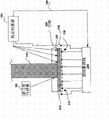
图5是表示根据本发明一方面的用于建立横跨坩埚的最佳热分布的加热器控制系统的示意图。5 is a schematic diagram illustrating a heater control system for establishing optimal heat distribution across a crucible in accordance with an aspect of the present invention.
图6是表示根据本发明一方面的坩埚中水平控制系统的示意图。6 is a schematic diagram illustrating a level control system in a crucible according to an aspect of the present invention.
具体实施方式Detailed ways
参考图1A和1B,在常规CZ系统中,在生长室102中在惰性气氛下将多晶硅片熔于熔融石英坩埚100中。室102中的气氛通常是氩气并且根据公知技术通过隔离阀104控制。硅容纳在刚好高于硅的熔点1412℃的温度下坩埚100中。然后将具有所需晶体取向的高质量籽晶在晶体提拉室106中下降以接触坩埚100中晶体熔体界面107处的熔体,并同时旋转。坩埚100同时反方向旋转,以促使熔体中的混合和使温度不均匀最小化。将一部分籽晶溶解于熔融硅中,以去除玷污(strained)的外部并暴露新的晶体表面。Referring to FIGS. 1A and 1B , in a conventional CZ system, a polycrystalline silicon wafer is melted in a fused
然后通过常规提拉机构108在晶体提拉室106中从熔体缓慢抬升或提拉籽晶。当籽晶上升时,它冷却并且来自熔体的材料粘附于它,因此形成较大的晶体或锭103。晶体或锭103的主体通过控制提拉速度以及熔融温度来生长,同时补偿坩埚中降低的熔体水平。即,随着晶体生长,坩埚100中的熔融硅被消耗。为了相对于布置在坩埚垂直壁周围的加热器补偿坩埚100中熔体的变化水平,坩埚100必须以小心可控的方式从起始晶体生长位置112垂直抬升到最后或最终位置114。The seed crystal is then slowly lifted or pulled from the melt in a
必须提供复杂机构以使坩埚的垂直移动与晶体的提拉相配合。坩埚的垂直移动必须在垂直方向上精确地与晶体的提拉相配合,这样小心地保持晶体和熔体之间的恒定界面并且晶体和熔体之间的界面关于加热器正确定位。Complex mechanisms must be provided to coordinate the vertical movement of the crucible with the pulling of the crystal. The vertical movement of the crucible must be precisely matched to the pulling of the crystal in the vertical direction so that a constant interface between the crystal and melt is carefully maintained and the interface between the crystal and melt is correctly positioned with respect to the heater.
晶体的直径通过减小或增加它的提拉速度和/或熔融温度来控制,直到达到所需的或目标直径。初始提拉速度通常相对较快。提拉持续到熔体几乎耗尽。设计提供坩埚垂直移动与晶体提拉机构精确配合的装置是非常昂贵的。The diameter of the crystal is controlled by decreasing or increasing its pulling rate and/or melting temperature until a desired or target diameter is achieved. The initial pull rate is usually relatively fast. Pulling continues until the melt is nearly exhausted. It is very expensive to design an apparatus that provides precise coordination of the vertical movement of the crucible with the crystal pulling mechanism.
图1A和1B示出与常规CZ坩埚和加热器布置相关的另外的缺点。常规CZ坩埚100的特征在于窄直径、高长宽比。为了容纳用于生长晶体的所有熔融硅,高长宽比是必须的,这是由于通常没有用于熔体补充的手段。作为替代,当坩埚中的硅被消耗时,坩埚100必须在垂直方向上移动(从起始位置112到最终位置114)以配合晶体的提拉。Figures 1A and 1B illustrate additional disadvantages associated with conventional CZ crucible and heater arrangements.
加热器元件118提供在坩埚100的周围并在熔体中产生温度分布,其不利地使加热器、坩埚壁、熔体以及悬浮在熔体中心的晶体之间的热梯度(DT)最大化,并且会导致坩埚壁达到过高温度。这不利地使晶体生长变慢。The
另外,在窄直径、高长宽比坩埚100中产生对流。对流不利地影响单晶硅的纯度。常规CZ坩埚100由诸如熔融石英的材料构成。熔融硅将常规熔融石英坩埚壁分解为硅和氧。对流擦洗坩埚壁并将氧和其它杂质传送到熔体中。这不利地影响生长晶体中的纯度和缺陷结构。对流还产生围绕生长晶体的不利热扰动,这可以招致缺陷进入晶体。In addition, convection is created in the narrow diameter, high
当晶体生长完成时,没有从坩埚100去除的残留熔融硅固化时大大膨胀并使坩埚破裂。典型CZ坩埚100因此是一次性使用的制品,在每一个硅锭生长之后即被抛去。When the crystal growth is complete, the residual molten silicon that is not removed from the
宽直径、低长宽比的坩埚Wide diameter, low aspect ratio crucibles
参考图2,根据本发明一方面的晶体生长系统提供固定的、宽直径、低长宽比坩埚200,坩埚200提供在生长室202中,生长室202又提供有底部201。常规隔离阀204以公知的方式在生长室202和多个晶体提拉室210a和210b中提供真空或者控制气氛。坩埚200的宽直径、低长宽比结构提供有使辐射热最小化的装置,例如热屏蔽205,用于使生长期间照射晶体或锭203的辐射能量最小。热屏蔽205是碳化硅、石墨或其它高温材料的平面部件,其支撑性地安装在生长室202的壁上并且具有尺寸与硅锭203相配合的内部孔。邻接孔的环形区域211向下朝熔体偏斜,以减少沿锭203的热流并且当锭从熔体222中移除时使热冲击最小化。Referring to FIG. 2 , a crystal growth system according to one aspect of the present invention provides a fixed, wide diameter, low
参考图3A,任选堰220布置在晶体/熔体界面和硅预熔化器208的出口228之间的熔体222中。堰220安置在坩埚200的底部上,或者作为替代,可以通过支撑装置例如在坩埚内壁上提供的任意方便的由惰性材料组成的支撑结构来支撑。堰220的顶部延伸到熔体222的表面之上。堰的目的是使来自预熔化器208的熔融硅能够分配到熔体中,而不在熔体中形成纹波或形成热扰动,这些波纹或热扰动会干扰熔体中的温度分布并且不利地影响正在生长的硅晶体224。堰220的特征在于相对于它的直径而言高度低,并且堰220通常是圆柱形,并且在延伸到熔体表面之下的堰部分中提供有孔,以使得可以在熔体中实现所需的热分布。Referring to FIG. 3A , an
宽直径、低长宽比生长坩埚200还防止或大大减少了在熔体中对流的形成以及对坩埚的附带擦洗作用,还减少了氧的引入。在优选实施方案中,坩埚的低长宽比(直径对高度)为4∶1-10∶1,优选约8∶1。相反,常规坩埚具有约1∶1-1∶4量级的长宽比。The wide diameter, low aspect
此外,环形加热元件以辐射状模式布置在坩埚底部上或尽可能接近坩埚底部,由于需要抬升机构因此这在常规CZ生长器中是不可能的。除了围绕坩埚周围布置的加热器之外,环形加热器在熔体中提供相应的加热区。这产生了贯穿熔体的基本水平的最佳热分布。还提供了最佳热分布,特别是在晶体和熔体之间的临界界面处。改进的温度控制提供了加速晶体生长,其超出了现有可能的晶体生长。Furthermore, the ring heating elements are arranged in a radial pattern on or as close as possible to the bottom of the crucible, which is not possible in conventional CZ growers due to the required lifting mechanism. In addition to the heaters arranged around the circumference of the crucible, ring heaters provide corresponding heating zones in the melt. This produces a substantial level of optimal heat distribution throughout the melt. It also provides optimal heat distribution, especially at the critical interface between crystal and melt. Improved temperature control provides accelerated crystal growth beyond what is currently possible.
粒状多晶硅在低长宽比坩埚中的熔化Melting of Granular Polycrystalline Silicon in a Low Aspect Ratio Crucible
常规坩埚具有高长宽比以及抬升机构,使得在晶体生长期间坩埚中熔体水平相对于坩埚侧面的加热器可以保持恒定。通常在坩埚底部下面没有加热器。Conventional crucibles have a high aspect ratio and a lift mechanism so that the level of melt in the crucible can be kept constant relative to heaters on the sides of the crucible during crystal growth. Usually there is no heater below the bottom of the crucible.
当这种坩埚装入多晶硅材料时,在熔体下降期间温度分布高度不均匀。在最接近加热器的坩埚壁处温度最高,并且在熔化材料的顶部和底部比中心更凉。当多晶硅是小颗粒(<1mm直径)、大表面积、在颗粒之间具有极小接触点以及空气是优良绝缘体的粒状形式时,该问题大大加剧。颗粒之间的热流趋向于在它们的接触点处将它们熔合在一起。其它热流通过辐射产生,在该阶段通过对流产生的极少。最接近加热器的颗粒首先熔融,在边缘和中心的那些跌落到坩埚的底部,留下横跨顶部表面的熔合颗粒桥以及桥下面的气孔。当然液体硅占据的体积远小于颗粒。组合效应将妨碍熔化过程,并且必须小心以免驱使接近加热器的熔融温度达到过高水平,否则污染物水平将增加。存在减少问题的技术,但是它们要求严格并且费时,例如,使坩埚向上抬升通过加热器,使得颗粒团的顶部首选熔融,而且应小心以免从侧面驱使太多的热。When such crucibles are filled with polysilicon material, the temperature distribution is highly inhomogeneous during the descent of the melt. The temperature is highest at the crucible wall closest to the heater and is cooler at the top and bottom of the molten material than in the center. This problem is greatly exacerbated when polysilicon is in granular form with small particles (<1 mm diameter), large surface area, very little contact points between particles and air is an excellent insulator. Heat flow between the particles tends to fuse them together at their points of contact. Other heat flows are generated by radiation and very little by convection at this stage. The particles closest to the heater melt first, and those at the edges and center fall to the bottom of the crucible, leaving bridges of fused particles across the top surface and air holes beneath the bridges. Of course liquid silicon occupies a much smaller volume than particles. The combined effect will hamper the melting process, and care must be taken not to drive the melting temperature close to the heater to excessively high levels, or contamination levels will increase. Techniques exist to reduce the problem, but they are demanding and time consuming, for example raising the crucible up past the heater so that the top of the pellet melts first, and care should be taken not to drive too much heat from the sides.
参考图3B,根据本发明的一方面,低长宽比坩埚200除侧面加热器219之外还具有以辐射状模式布置在其底部之下的多个环形加热器218,以提供更加均匀的温度分布,这是由于a)颗粒在坩埚中的深度较低和b)环形底部加热器218,所述环形底部加热器218以更加可控的分配横跨坩埚的整个底部表面积来施加热。环形底部加热器218优选是如有关图5所描述的单个可控的平面电阻加热元件。每一个加热元件218在熔体中产生相应加热区,以提供贯穿熔体的最佳温度分布。与高长宽比坩埚相比,颗粒和低长宽比坩埚的热壁之间的接触表面积更大,将更多的热驱使到颗粒中。因此,颗粒的整个团熔融更加均匀并且速度更加快,并且不附带与靠近加热器温度过高有关的污染。Referring to FIG. 3B, in accordance with an aspect of the present invention, the low
参考图3C,具有环形底部加热器218的低长宽比坩埚200实现了以贯穿熔体222的基本水平分布为特征的热梯度223。与分批次工艺相比,在使用低长宽比坩埚的连续工艺中,更容易传递热以熔融初始装料,这是由于:a)较少量的多晶硅“装料”在启动时熔融和b)预熔化器208提供液态硅以湿润颗粒,这在颗粒之间提供了更大面积的热接触并加速熔化过程。注意:预熔化器还被设计用以在颗粒周围提供均匀加热而不是从一侧加热,从而进一步增强熔化过程。Referring to FIG. 3C , a low
预熔化器Premelter
参考图3A、4和5,预熔化器208包含单独的容器,用于熔化一定量的固体原料并为生长坩埚200提供生长晶体的熔融材料的恒定源。在单晶硅的情况下,固态硅原料的源209例如硅片、块、颗粒或棒通过流控制器件212以足够补充生长坩埚的速度提供到预熔化器208。Referring to FIGS. 3A , 4 and 5 ,
预熔化器可以远离生长室单独布置,如图5和6所示。在优选实施方案中,预熔化器208包含提供在生长室202内部的独立容器,以熔化一定量的原料并将其提供到熔体222的表面。这有利地将预熔化器208置于可控气氛的生长坩埚222中,并使来自预熔化器的熔体需移动达到坩埚的距离最小化。The premelter can be located separately from the growth chamber, as shown in Figures 5 and 6. In a preferred embodiment,
参考图4,预熔化器包含熔化室400。预熔化器由能够耐高达约1590℃温度的石英材料构成。熔融碳化硅、结合碳化硅的氮化硅或类似材料也可用于预熔化器。一个或多个电阻加热器402适当地布置在熔化室下面或靠近熔化室布置,用于熔化一定量的固态晶体原料。任选的热导体404可以布置在加热器402和熔化室400之间。热导体404还是电绝缘体。热导体404散射来自加热器的热通量并降低由预熔化器石英壁可见的最大温度。热导体404还为温度超出约1590℃温度的石英熔化室提供机械支撑。加热器还任选地可布置在熔化室周围。Referring to FIG. 4 , the premelter includes a
掺杂剂和固态硅或晶体原料209的源通过流控制器312提供到熔化室400的第一部分中硅水平410处或之上的进口408。堰414限定包括进口408的熔化室第一部分416,并且还限定包括坩埚出口的第二部分418。熔化室400的独立第一部分416提供有进口408,以直接或通过原料和掺杂剂源209来接收预定量的固体掺杂剂材料。作为非限制性实例,掺杂剂材料可以是0.125×0.125×0.25英寸量级的重掺杂晶圆小片,加入速度至多10小片/锭。锭流中的后续锭将需要较少小片。所需掺杂剂小片的量是晶体生长时所吸收掺杂剂的量的函数。即,小片简单地注满从熔体吸附到晶体中的掺杂剂。将掺杂剂加入预熔化器中避免了可由固体块掺杂剂加入熔体中而产生的热扰动以及非均匀的温度分布,这种温度分布问题可由熔合潜热和热容量(质量×比热×DT)使掺杂剂材料高达熔融温度而产生。注意:这种热扰动温度与当直接将固态硅原料加入到熔体中很相似,但是减少很多。由于横跨熔体的最佳热梯度以及通过分别单个控制加热元件而控制熔体中的热区,可以在横跨生长晶体的半径范围内维持均匀热分布。因此,掺杂剂材料在进口408的加入可以在最终锭中提供基本均匀的轴向(纵向)和径向电阻率或电导率。第一堰414在第一部分416底部提供有流控制出口420。A source of dopants and solid silicon or
熔融硅从第一部分416的底部通过出口420进入熔化室400的第二部分418。然后熔融硅使第一部分中水平410升高。由于固态颗粒或未熔融的硅片浮动,关键的是在预熔化器中提供堰414,以确保仅仅熔融硅或晶体原料利用堰的流控制出口420流通到第一预熔化器部分416的底部然后从底部向上填充第二部分418。从出口424进入坩埚熔体的熔融硅或熔融晶体原料因此从预熔化器的底部被抽取。这种设置有利地保证了由于密度低于熔融硅而漂浮在熔融硅中的未熔融、固态材料不直接穿过从而到达熔化室400的第二部分418以及生长坩埚。Molten silicon enters the
出口管424还可用作第二堰并控制预熔化器的熔化室400中的熔体水平。出口管424包含具有进口以及在其远端的出口的管,所述进口接收来自熔化室400的第二部分418的熔融晶体原料,所述出口提供基本恒定的源,用于将熔融晶体原料补充到坩埚的熔体中。出口管424促使熔融晶体原料流沿其内表面进入生长坩埚的熔体中。The
出口管424的特征在于足够尺寸的内径,约1cm,以克服熔融原料的表面张力(熔融硅的表面张力比水高约30倍)。对于预熔化器中给定高差的熔融晶体原料,表面张力倾向于阻止或限制流过出口管。因此,管的直径被最优化以克服表面张力,同时使可引起坩埚中熔体过度扰动的飞溅影响最小化。出口管的远端位于坩埚中熔体水平之上的位置,选择一定的高度使得当将熔融原料和掺杂剂排入熔体以连续补充坩埚时扰动最小化。因此出口管的设计进一步在晶体熔体界面保持静态热条件,从而在最终晶锭中产生基本均匀的轴向(纵向)和径向电阻率或电导率。The
以这种方式,预熔化器208为生长坩埚200提供熔融硅的基本恒定的源,补充由生长晶体所吸收的硅。这使得生长坩埚200中的熔体能够相对于生长晶体保持在恒定的水平,而不需要坩埚垂直移动,并且还使得坩埚中的熔体水平能够根据需要增加或减少。这有利地消除了在常规CZ系统中必须用来使坩埚垂直移动以配合晶体提拉的复杂机构。这种通过预熔化器的补充还使加热器能够布置在坩埚的底部。本发明的这方面大大简化了生长单晶硅所需的装置并最终能够以较低成本加速生产单晶硅。In this manner,
通过使用预熔化器208而基本连续添加熔融硅消除了在关闭炉或加热元件以再装填坩埚200和再熔化硅中所涉及的时间消耗和能量浪费。使用熔融硅原料的基本连续源来补充熔体使得熔体与坩埚接触的时间最小,因此进一步限制了氧被吸收到熔体中。由于原硅在预熔化器中熔融的量非常小并且很快流入生长坩埚中,停留时间以及接触表面积同样被最小化。此外,不需要将生长室对环境大气开放以置换坩埚和提供新的硅装料的过程,该过程将新污染物引入生长室中。The substantially continuous addition of molten silicon through use of the
硅预熔化器208的另一个优点是,由于可以在再装填过程中加入掺杂剂,因此可以更好地控制晶体的轴向电阻。这有利地消除了在通过常规CZ法生长的晶体表现出的轴向电阻率梯度。熔体中偏析的影响以及晶体中所产生非均匀掺杂剂特征被基本消除。利用与生长坩埚200连通的独立硅预熔化器208的另一个优点是消除了硅装料的高温初始熔化,使生长坩埚上的应力最小化并减少沉淀到熔体中的氧。Another advantage of the
应该理解的是,预熔化器可以由惰性材料制成或涂覆,例如烧结的碳化硅或类似陶瓷,或者由其它相对于熔融硅具有惰性特征的材料涂覆,例如钽、铌或其氧化物和化合物,以减少熔体中的氧和其它杂质,这对坩埚是常有的情况。It should be understood that the premelter may be made of or coated with an inert material, such as sintered silicon carbide or similar ceramics, or with other materials having inert characteristics with respect to molten silicon, such as tantalum, niobium, or oxides thereof and compounds to reduce oxygen and other impurities in the melt, which is often the case for crucibles.
结合低长宽比、非反应性、烧结碳化硅坩埚200的硅预熔化器208以及晶体生长期间可控掺杂剂原料基本上消除了引起少数载流子复合的缺陷结构和位置的偏析、高纯度水平和氧沉淀。本发明的这方面在为高转换效率太阳能电池提供更高少数载流子寿命硅方面特别有用。The silicon premelter 208 in combination with the low aspect ratio, non-reactive, sintered
多个晶体提拉室Multiple crystal pulling chambers
再参考图2和3A,在旋转圆柱体212上提供多个提拉室210a、210b,圆柱体212又通过轴214来支撑。应该理解的是,多个提拉室210a、210b还可以布置成可移动、线型支撑元件,用于将每一个连续提拉室中的籽晶相继定位到生长室202内的坩埚200中的生长区中。多个提拉室210a、210b因此相对于生长室202可旋转或按序布置。当第一单晶硅锭完成时第一提拉室210a将完成的硅锭移出坩埚200中的生长区以及生长室202以冷却,后续提拉室210b移动来将新晶体定位于生长室202中并移到坩埚200中的晶体/熔体界面处的生长区。隔离阀206关闭以控制生长室202和相关提拉室中的气氛,并生长新的晶体。Referring again to FIGS. 2 and 3A , a plurality of pulling
提拉室210a、210b在坩埚200中生长区处的相继定位是连续过程中的最终步骤,使硅在生长坩埚中的停留时间最小化、消减了与冷却每一个晶体、变换新坩埚、再装填坩埚、排空生长室以及将装料再加热到熔融温度相关的时间;因此提供了具有高生产量的加速、连续晶体生长系统。而且,这种连续过程消除了生长坩埚的一次性使用的特征,并且使生长坩埚能够用于多个(10个或更多)晶体生长循环。The sequential positioning of the
坩埚的组成The composition of the crucible
再参考图2、3A、3B和3C,本发明另一方面提供低长宽比、宽直径的坩埚200,该坩埚由对熔融硅为惰性的材料构成,例如α或β烧结碳化硅、氮化钽或类似不含二氧化硅的陶瓷。作为替代方案,坩埚200的内部含硅表面可以根据公知技术提供有这种惰性材料涂层。这种理想的惰性材料由压缩并烧结的碳化硅颗粒和烧结助剂的混合物组成。与反应结合的碳化物不同,不存在游离硅。这种直接烧结材料没有金属相并因此耐化学侵袭。α碳化硅是指六角结构,β碳化硅是指立方结构。Referring again to Figures 2, 3A, 3B and 3C, another aspect of the present invention provides a low aspect ratio,
这种烧结碳化硅材料可以从CARBORUNDUM Corp.获得,名为SA-80;从GENERAL ELECTRIC获得,名为Sintride;和从KYOCERA获得,名为SC-201。This sintered silicon carbide material is available from CARBORUNDUM Corp. under the name SA-80; from GENERAL ELECTRIC under the name Sintride; and from KYOCERA under the name SC-201.
由上述烧结碳化硅材料组成的化学惰性生长坩埚200在常规CZ生长法中是未知的,这是由于常规坩埚是一次性使用后即丢弃的制品,并且没有在坩埚表面上提供烧结碳化硅或陶瓷坩埚或这种涂层的动机。A chemically
常规CZ生长法没有考虑使用坩埚材料例如烧结碳化硅,以基本消除氧向熔体中的引入。在常规CZ系统中,生长坩埚通常是在一次或两次生长循环之后即被丢去。因此,碳化硅涂层或由更高成本材料制成的坩埚将大大增加常规CZ系统的成本。应该理解是,出于同样的原因,这些材料还可有利地用于预熔化器中。Conventional CZ growth methods do not allow for the use of crucible materials such as sintered silicon carbide to substantially eliminate the introduction of oxygen into the melt. In conventional CZ systems, the growth crucible is typically thrown away after one or two growth cycles. Therefore, silicon carbide coatings or crucibles made of higher cost materials will add significantly to the cost of conventional CZ systems. It should be understood that these materials may also be advantageously used in premelters for the same reasons.
此外,源自生长坩埚壁的氧沉淀先前没有被认为是严重的问题,并且甚至可能在集成电路或其它电子器件中有益。氧从其它杂质趋向于积累的位置沉淀。这种氧沉淀可以以预定方式从有源器件区遥控定位到最终IC晶片中。然后氧沉淀用作吸引所不需要的杂质远离电学上的有源区域的收集位置,由此改进器件性能。Furthermore, oxygen precipitation originating from the walls of the growth crucible has not previously been considered a serious problem, and may even be beneficial in integrated circuits or other electronic devices. Oxygen precipitates from where other impurities tend to accumulate. This oxygen precipitation can be remotely localized in a predetermined manner from the active device area into the final IC wafer. The oxygen precipitate then serves as a collection site to attract unwanted impurities away from the electrically active region, thereby improving device performance.
但是,根据本发明的一方面,认为氧沉淀和相关的缺陷对将用于特定应用例如太阳能电池的硅中的少数电荷载流子寿命而言是问题。在太阳能电池中,如果在到达电接触之前,光电池中一些所产生的载流子在硅中缺陷、杂质或氧沉淀位置处复合,那么输出电流减少。跨越多个太阳能电池,这种缺陷会严重地减少输出电流。However, according to one aspect of the invention, oxygen precipitation and associated defects are believed to be problematic for minority charge carrier lifetime in silicon to be used in certain applications such as solar cells. In solar cells, if some of the generated carriers in the photovoltaic cell recombine at defect, impurity or oxygen precipitation sites in the silicon before reaching the electrical contacts, the output current decreases. Across multiple solar cells, this defect can severely reduce output current.
加热器和熔体温度控制Heater and Melt Temperature Control
图3B、3C和5表示提供温度的封闭环路控制的加热器和熔体温度控制系统,其特征在于横跨熔体的最佳温度分布和在熔体/晶体界面207处的固化区中均匀的最佳温度条件有助于控制晶体形成速度和进一步使缺陷密度最小化。3B, 3C and 5 show heater and melt temperature control systems that provide closed loop control of temperature, characterized by optimal temperature distribution across the melt and uniformity in the solidification zone at the melt/crystal interface 207. The optimal temperature conditions help to control the crystal formation rate and further minimize the defect density.
参考图3B和5,多个环形电阻加热元件218以辐射状模式布置在低长宽比坩埚200的下面。另外的电阻加热元件219围绕坩埚200外壁的周围布置。环形加热元件218和侧壁加热元件219由加热器控制240单个控制以产生独立的加热区,从而提供横跨熔体的最佳温度分布。加热器控制240包括微处理器控制器,用于对来自传感器234的信号作出响应从而控制并监测每一个加热器元件的作用时间、功率消耗以及由此的热输出。Referring to FIGS. 3B and 5 , a plurality of annular
对于每一个单独可控电阻加热元件可以维持所需的热输出,由此实现横跨熔体和横跨生长晶体半径范围的最佳温度分布。所需的热输出和所产生的温度分布通过加热器控制240的微处理器来测量每一个单独可控电阻加热元件的功率消耗来推出。每一个加热器的功率消耗对应于实现最佳温度分布所需的热输出。加热器控制240根据监测的功率消耗将功率施加到每一个加热器元件,以获得可重复状态,这样相应热区驱使热均匀地进入熔体中。应该理解的是,有利的加热器布置和可控热区还可用于驱使热均匀进入包括固体颗粒的熔融材料。加热器布置还可用于均匀加热和熔融固体,例如颗粒、颗粒和片的组合以及固态晶体原料的片或块。由于在低长宽比坩埚下面单独控制的加热器的最佳布置,横跨固态材料片之间的接触点进入原料的热通道被最小化。当使用小片或颗粒时,这是特别重要的,这是由于给定团块或材料的相邻片或颗粒之间具有更多的接触点,因此减少或限制了热流。这有效地在坩埚中提供更大的接触表面积并缩短进入包括固体材料的原料的热通道。The desired heat output can be maintained for each individually controllable resistive heating element, thereby achieving an optimal temperature distribution across the melt and across the radius of the growing crystal. The desired heat output and resulting temperature profile are derived by the
这克服了在常规CZ系统中的问题,在常规CZ系统中,最靠近加热器的固体材料特别是小片和颗粒首先熔融并且在边缘和中心的那些跌落到坩埚的底部,留下横跨顶部表面的熔合颗粒桥以及桥下面的气孔。This overcomes a problem in conventional CZ systems where the solid material closest to the heater, especially small flakes and particles, melts first and those at the edges and center fall to the bottom of the crucible, leaving a crucible across the top surface. The fused particle bridges and the pores below the bridges.
因此,横跨熔体建立了代表最佳热分布的一系列热区。每一个热区对应于独立可控电阻加热器元件218的热输出。包含一个或多个光学高温计的温度传感器234采集横跨熔体的每一个独立热区的温度读数,每一个热区由相应加热器元件控制。单个高温计也可以扫描独立的区,提供代表各区温度的在线输出信号236。温度传感器234还可以包括热电偶,用于检测围绕坩埚200周围布置的外加热元件219的温度。Thus, a series of hot zones representing optimal heat distribution are established across the melt. Each thermal zone corresponds to the heat output of an independently controllable
根据标准封闭环路负载调节技术,温度传感器234将代表各个热区温度的在线信号236发送到加热器控制单元240。加热器控制单元240将相应激活信号发送到每一个加热元件,以将加热元件维持在预定范围。在实现了所需的控制设定点之后,加热器和熔体温度可以维持在窄范围。应该理解的是,电阻加热元件218的分别控制在坩埚壁和晶体之间提供最佳温度分布。提拉的速度(晶体生长速度)通过在晶体和熔体之间界面处的温度分布来控制。因此,本发明的该方面提供了横跨熔体基本水平维持的最佳温度分布,特别是在晶体熔体界面处提供了前所未有的更大控制的最佳温度分布。应该理解的是,这种最佳温度分布是通过宽的长宽比坩埚结合布置在坩埚下面或周围的单独控制加热元件以及较浅深度的熔体来实现的。The
再参考图4,由于经固态硅原料引入熔体中可引起温度扰动,因此通过硅预熔化器208实现熔体的改进控制,其中硅的所有熔化均在坩埚外部完成。固态硅原料源209包含各种形式的硅原料,例如粉碎的硅、片、块、来自流化床的颗粒、硅棒等。Referring again to FIG. 4, since the introduction of solid silicon feedstock into the melt can cause temperature disturbances, improved control of the melt is achieved through the
如图5所示,预定直径的晶体244可以用主动反馈来精密地控制。当晶体利用常规光学图案识别技术生长时,利用包含照相机或类似光检测器系统的弯月面传感器232来监测晶体直径。晶体生长在晶体244和熔体222之间的弯月面界面207处发生并且调节提拉速度以产生所需晶锭直径。以这种方法,利用主动反馈可以精密地控制预定晶体直径和晶体生长速度。As shown in FIG. 5, a
水平控制level control
参考图6,在优选实施方案中,通过主动反馈系统检测生长坩埚中硅熔体重量和调节提供给预熔化器的硅原料的量以及从预熔化器208排放到熔体中的熔融硅的量或速度,从而实现生长坩埚200中熔体222以及熔融硅原料从预熔化器208排放到熔体222中的速度的改进水平控制。Referring to FIG. 6, in a preferred embodiment, the weight of the silicon melt in the growth crucible is sensed and the amount of silicon feedstock supplied to the premelter and the amount of molten silicon discharged from the
用于测定未装填以及装填有所需水平熔体的生长坩埚的重量的敏感装置由重量传感器300来提供。适合的重量传感器300包括一个或多个基于应变计的测压元件(load cell)。每一个测压元件均是将作用在其上的负荷或重量转换为代表该负荷的电信号的转换器。坩埚200中硅熔体的重量使得与坩埚200接触的机械杆或臂304的产生偏转。这反过来又产生与负荷成比例的电阻变化。测压元件或重量传感器300随后产生代表熔体222重量的输出信号,经通信连接308输送到基于微处理器的水平控制器306。通信连接308可以是电缆或光纤、远红外或无线连接以提供稳定的高温操作。Sensitive means for determining the weight of the growth crucible unfilled as well as filled with the desired level of melt is provided by
水平控制器306对重量传感器300响应从而产生输出信号,经通信连接310激励分配器或流控制器312,该控制器312控制释放预定量的固态硅原料209进入预熔化器208。水平控制器306包含微处理器,该微处理器用于测定基于生长坩埚中熔体所需深度D的预熔化器输出。根据本发明一方面,这是由下列关系式确定的:
D=(W-Wt)/(πR2r)D=(W-Wt)/(πR 2 r)
其中W是包含熔体222的坩埚200的总重量;Wt是未装载时测量的坩埚200的重量;R是坩埚的内径;r是液态硅的密度。where W is the total weight of the
以这种方式,可以控制预熔化器中硅的水平和熔体222的水平。In this way, the level of silicon in the premelter and the level of the
应该理解的是,上述系统提供预熔化器的最佳输出能力并使得能够实现预熔化器和生长坩埚的精密控制的最佳补充。通过利用远低于常规CZ方法中的熔体装料来进行晶体生长,这有利地增加生产量,并且还有助于减少硅在坩埚中的停留时间以及附带减少杂质。通过晶体生长和从预熔化器截流的组合,这还使得新晶体能够在清空坩埚之后更快地开始。It should be appreciated that the system described above provides optimum output capability of the premelter and enables optimal replenishment of the premelter and growth crucible with close control. By performing crystal growth with a much lower melt charge than in conventional CZ processes, this advantageously increases throughput and also helps to reduce the residence time of silicon in the crucible and incidental impurities. This also enables faster initiation of new crystals after the crucible has been emptied, through a combination of crystal growth and shutoff from the premelter.
本发明上述特征提供单晶硅生长方法,该方法使进入熔体中的沉淀氧最小化并且使熔体中杂质和偏析最小化或被消除。由于这些因素使得产生载流子复合位置的杂质水平和缺陷结构最小化,因此本发明方法在硅中直接实现了增加的少数载流子寿命。由于简化的晶体生长装置,与现有可能的生长速度和成本相比,可以以更高的生长速度和更低的成本来实现这种具有增加的少数载流子寿命的硅。由根据本发明方法生产的硅在提供更高效、低成本高寿命太阳能电池方面具有特别的优势。The above features of the present invention provide a silicon single crystal growth method that minimizes the ingress of precipitated oxygen into the melt and minimizes or eliminates impurities and segregation in the melt. As these factors minimize impurity levels and defect structures that create carrier recombination sites, the inventive method achieves increased minority carrier lifetime directly in silicon. Due to the simplified crystal growth setup, such silicon with increased minority carrier lifetime can be realized at higher growth rates and lower costs than currently possible. Silicon produced by the method according to the invention has particular advantages in providing more efficient, low cost and long life solar cells.
工业适用性Industrial applicability
范围scope
虽然结合目前被认为是最实用和优选的实施方案描述了本发明,但应该理解的是,本发明并不限于上述公开的实施方案和替代方案,相反,本发明旨在覆盖包括在所附权利要求范围内的各种修改和等价布置。例如,可按照CZ方法生长的其它材料可用作熔融材料,例如砷化镓、磷化镓、蓝宝石以及各种金属、氧化物和氮化物。而且,抵抗由熔融硅引起的破坏的其它材料例如陶瓷涂层或各种金属、氧化物、氮化物以及它们的组合也可以用于坩埚的组成,或者作为坩埚内壁上的涂层。While the invention has been described in connection with what are presently considered to be the most practical and preferred embodiments, it should be understood that the invention is not limited to the above disclosed embodiments and alternatives, but rather the invention is intended to cover Various modifications and equivalent arrangements are within the scope of the claims. For example, other materials that can be grown according to the CZ method can be used as molten materials, such as gallium arsenide, gallium phosphide, sapphire, and various metals, oxides, and nitrides. Furthermore, other materials resistant to damage caused by molten silicon such as ceramic coatings or various metals, oxides, nitrides and combinations thereof may also be used in the composition of the crucible, or as a coating on the inner walls of the crucible.
可以提供单独的堰或隔板以保护晶体免受对流和热扰动。可以提供多个提拉室以连续提拉相继的晶体,而不必在坩埚之上的适当位置处旋转。重要的是,一系列晶体提拉室相继位于坩埚之上,以重复基本连续的晶体生长,而不需要在每一个生长循环之后移除坩埚。因此,本领域普通技术人员应该理解,所有的这种等价布置和修改均包括在所附权利要求的范围内。Separate weirs or baffles can be provided to protect the crystals from convection and thermal disturbances. Multiple pulling chambers may be provided to successively pull successive crystals without having to rotate in place above the crucible. Importantly, a series of crystal pulling chambers are positioned sequentially above the crucible to repeat substantially continuous crystal growth without the need to remove the crucible after each growth cycle. Therefore, it should be understood by those skilled in the art that all such equivalent arrangements and modifications are included within the scope of the appended claims.
序列清单sequence list
以下内容对应于母案申请中的原始权利要求书,现作为说明书的一部分并入此处:The following correspond to the original claims in the parent application, which are hereby incorporated as part of the specification:
1.一种用于从熔融晶体原料生长单晶锭的改进CZ系统,包括:1. An improved CZ system for growing single crystal ingots from molten crystal feedstock comprising:
包括底部和侧壁的低长宽比、宽直径坩埚,用于容纳与从熔融材料生长锭的籽晶相关的熔体/晶体界面处的一定量熔融材料;a low aspect ratio, wide diameter crucible including a bottom and sidewalls for containing a quantity of molten material at the melt/crystal interface associated with growing a seed crystal of an ingot from the molten material;
预熔化器,用于为坩埚提供熔融晶体原料的基本连续源,使得熔体/晶体界面维持在所需水平而没有坩埚的垂直移动;A premelter for providing a substantially continuous source of molten crystal feedstock to the crucible such that the melt/crystal interface is maintained at the desired level without vertical movement of the crucible;
布置在坩埚底部之下的环形加热装置,用于横跨熔体和在晶体熔体界面处为最佳晶体生长提供均匀热分布。Annular heating arranged below the bottom of the crucible to provide uniform heat distribution across the melt and at the crystal-melt interface for optimal crystal growth.
2.如项1中的改进CZ系统,其中环形加热装置包括以辐射状模式布置的多个独立控制的电阻加热器,以建立横跨熔体的相应热区,每一个热区由各电阻加热器的热输出控制,使得横跨熔体和在晶体熔体界面处建立最佳热分布。2. The improved CZ system as in item 1, wherein the annular heating means comprises a plurality of independently controlled resistance heaters arranged in a radial pattern to create respective thermal zones across the melt, each heated by a respective resistance The heat output of the device is controlled so that an optimal heat distribution is established across the melt and at the crystal-melt interface.
3.如项1中的改进CZ系统,还包括:3. The improved CZ system as in item 1, also includes:
一个或多个分别控制的侧壁加热器以及一个或多个用于监测每一个热区温度和用于产生代表检测温度的信号的传感器;one or more individually controlled side wall heaters and one or more sensors for monitoring the temperature of each hot zone and for generating a signal representative of the detected temperature;
对传感器信号作出响应的控制装置,用于激活每一个侧壁加热器和环形加热装置,使得横跨熔体和在晶体熔体界面处建立最佳热分布。Control means, responsive to sensor signals, is used to activate each of the sidewall heaters and annular heating means so as to establish optimum heat distribution across the melt and at the crystal-melt interface.
4.如项1中的改进CZ生长器,还包括多个相继关于坩埚布置的晶体提拉室,每一个提拉室包括用于在熔体/晶体界面处定位籽晶和用于提拉生长锭的装置,使得当第一锭的生长完成时第一提拉室将第一锭移离坩埚以冷却,并且后续提拉室移动来将新晶体定位于坩埚中的熔体/晶体界面处。4. The improved CZ grower as in item 1, further comprising a plurality of crystal pulling chambers successively arranged with respect to the crucible, each pulling chamber including a crystal for positioning the seed crystal at the melt/crystal interface and for pulling growth The ingots are arranged such that a first pulling chamber moves the first ingot away from the crucible to cool when growth of the first ingot is complete, and subsequent pulling chambers move to position new crystals at the melt/crystal interface in the crucible.
5.如项1中的改进CZ系统,其中坩埚的低长宽比(直径对高度)为4∶1-10∶1,优选约8∶1。5. The improved CZ system as in item 1, wherein the crucible has a low aspect ratio (diameter to height) of 4:1-10:1, preferably about 8:1.
6.如项1中的用于连续生长单晶锭的系统,还包括用于将一定量的掺杂剂材料加入到预熔化器中使得整个锭中掺杂剂浓度周向和径向基本均匀的装置。6. The system for continuously growing a single crystal ingot as in item 1, further comprising adding a certain amount of dopant material into the premelter so that the dopant concentration in the entire ingot is substantially uniform in the circumferential and radial direction installation.
7.如项1或5中的改进CZ系统,还包括:7. The improved CZ system as in item 1 or 5, also includes:
低长宽比、宽直径坩埚,该坩埚具有涂覆有选自α或β烧结碳化硅、氮化钽或类似陶瓷的材料的内表面,用于容纳熔融材料。A low aspect ratio, wide diameter crucible having an inner surface coated with a material selected from alpha or beta sintered silicon carbide, tantalum nitride or similar ceramics for containing molten material.
8.如项1或5中的改进CZ系统,还包括:8. The improved CZ system as in item 1 or 5, also includes:
低长宽比、宽直径坩埚,该坩埚包含选自α或β烧结碳化硅、氮化钽或类似陶瓷的材料。A low aspect ratio, wide diameter crucible comprising a material selected from alpha or beta sintered silicon carbide, tantalum nitride or similar ceramics.
9.一种用于连续生长单晶锭的系统,包括:9. A system for continuously growing a single crystal ingot, comprising:
包括底部的低长宽比、大直径坩埚,用于容纳晶体材料的熔体;A low aspect ratio, large diameter crucible including a bottom to hold a melt of crystalline material;
预熔化器,该预熔化器具有用于接收晶体材料供给的进口、用于熔化所述材料的装置和用于当熔体被生长晶体吸收时补充熔体的与坩埚连通的出口,使得坩埚中的熔体相对于晶体维持在所需水平而没有坩埚的垂直移动;a premelter having an inlet for receiving a supply of crystalline material, means for melting said material and an outlet in communication with the crucible for replenishing the melt as it is absorbed by the growing crystal such that the The melt is maintained at the desired level relative to the crystal without vertical movement of the crucible;
多个相继关于坩埚布置的晶体提拉室,使得在生长第一锭时第一提拉室将第一锭移离坩埚以冷却,并且后续提拉室移动来将新晶体定位于坩埚中。A plurality of crystal pulling chambers are arranged in succession about the crucible such that a first pulling chamber moves the first ingot away from the crucible to cool as it grows, and subsequent pulling chambers move to position new crystals in the crucible.
分别可控的加热装置,靠近坩埚底部布置,用于横跨熔体和在晶体熔体界面处为改进晶体生长提供最佳热分布。Separately controllable heating means, arranged near the bottom of the crucible, are used to provide optimum heat distribution across the melt and at the crystal-melt interface for improved crystal growth.
10.如项9中的用于连续生长单晶锭的系统,还包括布置在晶体/熔体界面和预熔化器出口之间的熔体中的堰;该堰包括在熔体上方延伸的顶表面,以阻止当将预熔化器中的熔融材料分配到熔体中时在熔体中形成波纹或热扰动。10. The system for continuously growing a single crystal ingot as in item 9, further comprising a weir arranged in the melt between the crystal/melt interface and the outlet of the premelter; the weir comprises a top extending above the melt surface to prevent ripples or thermal disturbances in the melt as molten material from the premelter is dispensed into the melt.
11.一种用于从熔融晶体原料生长单晶锭的改进CZ系统,包括:11. An improved CZ system for growing single crystal ingots from molten crystal feedstock, comprising:
低长宽比、宽直径坩埚,用于容纳与从熔融材料生长锭的籽晶相关的熔体/晶体界面处的一定量熔融材料;A low aspect ratio, wide diameter crucible for containing a volume of molten material at the melt/crystal interface associated with growing a seed crystal of an ingot from the molten material;
预熔化器,用于接收固态晶体原料和掺杂剂的源和为坩埚提供熔融掺杂晶体原料的基本连续源;a premelter for receiving a source of solid crystal feedstock and dopant and for providing a substantially continuous source of molten doped crystal feedstock to the crucible;
分别可控的加热装置,围绕坩埚侧面和靠近坩埚底部布置,用于横跨熔体和在晶体熔体界面处为改进晶体生长提供最佳热分布。Separately controllable heating means, arranged around the sides of the crucible and near the bottom of the crucible, are used to provide optimal heat distribution across the melt and at the crystal-melt interface for improved crystal growth.
12.对用于从熔融晶体原料生长单晶锭的CZ系统的改进,包括:12. Improvements to CZ systems for growing single crystal ingots from molten crystal feedstock, including:
用于容纳熔融晶体原料的低长宽比、宽直径坩埚,该坩埚包含选自α或β烧结碳化硅或类似陶瓷的材料。A low aspect ratio, wide diameter crucible for containing molten crystalline feedstock comprising a material selected from alpha or beta sintered silicon carbide or similar ceramics.
13.对用于从熔融晶体原料生长单晶锭的CZ系统的改进,包括:13. Improvements to CZ systems for growing single crystal ingots from molten crystal feedstock, including:
低长宽比、宽直径坩埚,该坩埚具有涂覆有选自α或β烧结碳化硅、氮化钽或类似陶瓷的材料的内表面,用于容纳熔融原料。A low aspect ratio, wide diameter crucible having an inner surface coated with a material selected from alpha or beta sintered silicon carbide, tantalum nitride or similar ceramics for containing molten feedstock.
14.一种用于从置于坩埚中生长界面处的籽晶来生长锭的改进CZ系统,包括用于使接收自源的固态晶体原料熔融和为坩埚提供熔融晶体原料输出的预熔化器,该系统包括:14. An improved CZ system for growing an ingot from a seed crystal placed at a growth interface in a crucible comprising a pre-melter for melting solid crystal feedstock received from a source and providing an output of molten crystal feedstock to the crucible, The system includes:
测压元件装置,用于检测坩埚中熔体的重量和产生代表该检测重量的输出信号;a load cell arrangement for sensing the weight of the melt in the crucible and generating an output signal representative of the sensed weight;
水平控制器,包括对来自测压元件的信号作出响应的微处理器,用于确定基于生长坩埚中熔体的所需深度D的预熔化器输出;a level controller including a microprocessor responsive to a signal from the load cell for determining a premelter output based on a desired depth D of melt in the growth crucible;
流控制装置,与水平控制器通信连接并且布置在固态原料源和预熔化器之间,用于对来自水平控制器的信号响应从而截取或分配来自源的原料至预熔化器,使得预熔化器输出将坩埚中熔体水平维持在最佳晶体生长的预定深度。a flow control device in communication with the level controller and disposed between the source of solid feedstock and the premelter for intercepting or distributing feedstock from the source to the premelter in response to a signal from the level controller such that the premelter The output maintains the melt level in the crucible at a predetermined depth for optimum crystal growth.
15.一种从置于熔融材料中晶体/熔体界面处的籽晶来改进单晶锭生长的方法,包括:15. A method for improving the growth of a single crystal ingot from a seed placed at a crystal/melt interface in a molten material, comprising:
在低长宽比、宽直径坩埚中容纳熔融材料,以减少熔体中的对流和热变化;Contains molten material in a low aspect ratio, wide diameter crucible to reduce convection and thermal changes in the melt;
在预熔化器中熔化固态晶体材料,为坩埚提供熔融材料的基本连续的补充,从而将坩埚中的晶体/熔体界面维持在所需水平;melting solid crystalline material in a premelter to provide a substantially continuous replenishment of molten material to the crucible, thereby maintaining the crystal/melt interface in the crucible at a desired level;
在坩埚下面提供多个加热器,用于横跨熔体建立相应热区;Multiple heaters are provided below the crucible to create corresponding thermal zones across the melt;
控制加热器的热输出,用于横跨熔体和在晶体/熔体界面处为改进晶体生长提供最佳热分布。Heat output from the heater is controlled to provide optimal heat distribution across the melt and at the crystal/melt interface for improved crystal growth.
16.根据项15的方法,其中为坩埚提供熔融材料的基本连续的补充从而将晶体/熔体界面维持在所需水平的步骤还包括:16. The method according to item 15, wherein the step of providing the crucible with a substantially continuous replenishment of molten material to maintain the crystal/melt interface at a desired level further comprises:
测定坩埚中未装填和装填所需深度的熔体时坩埚的重量;Determination of the weight of the crucible when it is not filled and when it is filled with the required depth of melt;
检测晶体生长期间生长坩埚的实际重量;和基于晶体生长期间坩埚和熔体的实际重量和含有所需深度熔体的坩埚的测定重量之间的差异,通过驱动分配器以释放预定量的固态晶体原料进入预熔化器从而在坩埚中维持所需深度的熔体来控制预熔化器的输出。detecting the actual weight of the growth crucible during crystal growth; and releasing a predetermined amount of solid crystals by actuating the dispenser based on the difference between the actual weight of the crucible and melt during crystal growth and the measured weight of the crucible containing the melt at the desired depth Feedstock enters the premelter to maintain the desired depth of melt in the crucible to control the output of the premelter.
17.一种改进的单晶材料,其特征在于高的少数载流子寿命,该单晶材料通过包括下列步骤的方法制成:17. An improved single crystal material characterized by a high minority carrier lifetime, the single crystal material being made by a method comprising the steps of:
从籽晶生长单晶材料,该籽晶容纳在宽直径、低长宽比坩埚中的晶体熔体界面处,以防止形成对流和使熔体中的氧最少化;Growth of single crystal material from a seed crystal housed at the crystal-melt interface in a wide-diameter, low-aspect-ratio crucible to prevent the formation of convection currents and minimize oxygen in the melt;
在预熔化器中熔化晶体原料,用于坩埚中熔体的无扰动补充;Melting crystal feedstock in a premelter for undisturbed replenishment of the melt in the crucible;
横跨熔体提供多个分别可控的热区,使得横跨熔体以及特别是在熔体晶体界面处产生最佳热分布。A plurality of individually controllable thermal zones are provided across the melt such that an optimal heat distribution is produced across the melt and especially at the crystallographic boundaries of the melt.
18.对用于从置于熔融材料中晶体熔体界面处的晶体来生长锭的系统的改进,所述熔融材料容纳在具有可控气氛的坩埚中,所述改进包括:18. An improvement to a system for growing an ingot from a crystal placed at a crystal melt interface in a molten material contained in a crucible having a controlled atmosphere, the improvement comprising:
布置在坩埚可控气氛中的预熔化器,用于为坩埚提供熔融晶体原料的连续源,使得晶体熔体界面相对于生长锭维持在所需水平而没有坩埚的垂直移动;a premelter disposed within the controlled atmosphere of the crucible for providing a continuous source of molten crystal feedstock to the crucible such that the crystal melt interface is maintained at a desired level relative to the growing ingot without vertical movement of the crucible;
包括熔化室的预熔化器,所述熔化室包括具有接收固态晶体原料源的进口的第一部分和包括出口的第二部分,所述出口具有基本布置在坩埚中熔体水平处的出口端,用于为坩埚提供熔融原料的无扰动分布;和A premelter comprising a melting chamber comprising a first portion having an inlet for receiving a source of solid crystalline feedstock and a second portion comprising an outlet having an outlet end disposed substantially at the level of a melt in a crucible for to provide an undisturbed distribution of molten feedstock to the crucible; and
靠近熔化室提供的加热器,用于熔化固态晶体原料;和a heater provided adjacent to the melting chamber for melting the solid crystalline feedstock; and
布置在熔化室中的堰,用于限定第一和第二部分,使得从第一部分的底部向上来填充第二部分,由此防止任意未熔融的、固态晶体原料进入坩埚。A weir is arranged in the melting chamber to define the first and second portions such that the second portion is filled from the bottom of the first portion upwards, thereby preventing any unmelted, solid crystal feedstock from entering the crucible.
19.如项18中的系统,还包括:19. The system in item 18, further comprising:
对坩埚中晶体熔体界面水平作出响应的控制装置,该装置与固态晶体原料的源连接,以可控地将固态晶体原料分配到预熔化器中,使得坩埚中熔融材料的深度维持在最佳晶体生长的所需水平;和control means responsive to the interface level of the crystal melt in the crucible, connected to a source of solid crystal material for controllably dispensing the solid crystal material into the premelter such that the depth of molten material in the crucible is maintained at an optimum the desired level of crystal growth; and
其中熔化室的出口包括具有进口和出口的第二堰,用于将熔融原料连续补充到坩埚中。Wherein the outlet of the melting chamber includes a second weir having an inlet and an outlet for continuously replenishing molten raw material into the crucible.
20.如项19中的系统,其中第二堰包括特征在于具有足够尺寸的内径的管,以克服表面张力的影响和/或使热扰动最小化,同时维持熔融原料向坩埚中的补充。20. The system of item 19, wherein the second weir comprises a tube characterized by an inner diameter of sufficient size to overcome the effects of surface tension and/or minimize thermal disturbances while maintaining replenishment of molten feedstock to the crucible.
21.预熔化器,用于为在其中的晶体熔体界面处生长锭的坩埚提供熔融晶体原料的连续流,该预熔化器包括:21. A premelter for providing a continuous flow of molten crystal feedstock to a crucible in which an ingot is grown at a crystal melt interface, the premelter comprising:
具有接收固态晶体原料的进口和出口的熔化室,所述出口具有基本布置在晶体熔体界面水平处的远端,用于为坩埚提供熔融晶体原料的基本连续的补充;a melting chamber having an inlet for receiving solid crystal feedstock and an outlet for providing a substantially continuous replenishment of molten crystal feedstock to the crucible, the outlet having a distal end disposed substantially at the level of the crystal melt interface;
靠近熔化室的加热器,用于使熔融晶体原料熔融;a heater adjacent to the melting chamber for melting the molten crystal feedstock;
堰,提供在进口和出口之间的熔化室中,以引导熔融晶体原料在堰之下向下流并且向上流入出口,由此防止由于密度低于熔融原料而不需要的固态晶体原料经过出口到达坩埚。a weir provided in the melting chamber between the inlet and the outlet to direct the molten crystal feedstock to flow downwardly under the weir and upwardly into the outlet, thereby preventing undesired solid crystal feedstock due to its lower density than the molten feedstock from passing through the outlet to the crucible .
22.根据项21的装置,还包括:22. The device according to item 21, further comprising:
用于检测坩埚中熔融材料的重量的装置,所述重量对应于与锭的生长相关的晶体熔体界面的最佳水平;means for detecting the weight of the molten material in the crucible, said weight corresponding to the optimum level of the crystal-melt interface in relation to the growth of the ingot;
控制装置,具有对检测装置作出响应的输入和与固态晶体原料源连接的输出引线,用于可控地将固态晶体原料分配到预熔化器中,使得在坩埚中维持最佳的锭生长。A control means having an input responsive to the detection means and an output lead connected to a source of solid crystal feedstock for controllably dispensing the solid crystal feedstock into the premelter such that optimal ingot growth is maintained in the crucible.
23.一种用于在坩埚中基本均匀熔化晶体原料的装料的改进方法,所述装料包括特征在于主要尺寸在小至1mm或更小量级上的固体块、棒或颗粒,所述改进方法包括:23. An improved method for substantially uniformly melting a charge of crystalline feedstock in a crucible, said charge comprising solid blocks, rods or granules characterized by major dimensions on the order of as little as 1 mm or less, said Ways to improve include:
在以低长宽比和宽直径底部为特征的坩埚中容纳晶体原料;Hold crystal feedstock in crucibles characterized by low aspect ratios and wide diameter bottoms;
在坩埚底部下面提供多个独立可控的加热器,以横跨坩埚建立多个可控热区,这样由于更大的接触表面积以及进入坩埚中装料的更短热通道,热被均匀地驱入颗粒中;Multiple independently controllable heaters are provided below the bottom of the crucible to create multiple controllable thermal zones across the crucible so that heat is dissipated evenly due to the greater contact surface area and shorter thermal path into the charge in the crucible into the particles;
激活每一个加热器,使得每一个加热器的热输出提供通过装料的最佳温度分布,从而均匀并快速地熔化颗粒;Activation of each heater so that the heat output of each heater provides an optimal temperature distribution through the charge to melt the pellets evenly and rapidly;
通过测量每一个加热器相对于快速实现均匀熔化颗粒所需时间的功率消耗,从而测定最佳温度分布;和Determining the optimum temperature profile by measuring the power consumption of each heater relative to the time required to rapidly achieve uniform melting of the particles; and
根据所测定的功率消耗,将功率施加到每一个加热器,从而控制每一个加热器。Each heater is controlled by applying power to each heater based on the measured power consumption.
24.一种用于在坩埚中基本均匀熔化晶体原料的装料的装置,所述装料包括特征在于主要尺寸在小至1mm或更小量级上的固体块、棒或颗粒,所述装置包括:24. An apparatus for substantially uniformly melting a charge of crystalline feedstock in a crucible, said charge comprising solid blocks, rods or granules characterized by major dimensions on the order of as little as 1 mm or less, said apparatus include:
低长宽比、宽直径坩埚底,用于容纳熔融晶体原料;Low aspect ratio, wide diameter crucible bottom for containing molten crystal feedstock;
提供在坩埚底部下面的多个独立可控的加热器,用于横跨坩埚中熔融晶体原料建立相应热区,这样由于更大的接触表面积以及进入坩埚中包括固体材料的装料的更短热通道,热被均匀地驱入颗粒中;和A plurality of independently controllable heaters are provided below the bottom of the crucible for establishing a corresponding thermal zone across the molten crystal feedstock in the crucible, such that due to the greater contact surface area and shorter thermal channels, heat is driven uniformly into the particles; and
用于施加功率的装置,用于热激活每一个加热器以实现最佳温度分布,使得热区以所需的速度将热均匀地驱入固体材料中。Means for applying power to thermally activate each heater for optimum temperature distribution so that the hot zone drives heat uniformly into the solid material at the desired rate.
25.根据项24的装置,还包括:25. The device according to item 24, further comprising:
控制装置,用于监测实现最佳温度分布所需的每一个加热器的功率消耗和用于根据所测定的功率消耗来施加功率以热激活每一个加热器,从而以所需速度实现颗粒均匀熔化的可重复状态。Control means for monitoring the power consumption of each heater required to achieve an optimum temperature profile and for applying power to thermally activate each heater in accordance with the measured power consumption to achieve uniform melting of the particles at the desired rate repeatable state.
26.根据项24的装置,其中坩埚的直径对高度的低长宽比为4∶1-10∶1,优选约8∶1。26. The device according to item 24, wherein the crucible has a low aspect ratio of diameter to height of 4:1 to 10:1, preferably about 8:1.
27.一种用于在坩埚中基本均匀熔化硅或多晶硅晶体材料的装料的装置,所述装料包括下至主要尺寸在1mm或更小量级上的固体块、棒或颗粒,所述装置包括:27. An apparatus for substantially uniformly melting a charge of silicon or polysilicon crystalline material in a crucible, said charge comprising solid blocks, rods or pellets down to major dimensions on the order of 1 mm or less, said Devices include:
低长宽比、宽直径坩埚,用于容纳硅或多晶硅熔体;Low aspect ratio, wide diameter crucibles for containing silicon or polysilicon melts;
布置在坩埚之下的多个独立可控的加热器,用于建立穿过熔体的相应热区,这样热被均匀地驱入到更大的接触表面积中以及通向坩埚中包括固体材料的装料的更短热通道中;Multiple independently controllable heaters arranged under the crucible to create corresponding hot zones across the melt so that heat is driven uniformly into a larger contact surface area and to the solid material in the crucible In the shorter hot aisle of charging;
用于热激活每一个加热器的装置,以实现横跨熔体的最佳热分布,使得颗粒以所需速度均匀熔化;和Means for thermally activating each heater to achieve optimal heat distribution across the melt so that particles melt uniformly at the desired rate; and
控制装置,用于通过监测被每一个加热器所消耗的功率来选择性控制每一个加热器的热激活,以实现横跨熔体的最佳热分布。Control means for selectively controlling the thermal activation of each heater by monitoring the power consumed by each heater to achieve optimal heat distribution across the melt.
28.根据项27的装置,其中坩埚的低长宽比(直径对高度)为4∶1-10∶1,最优选约8∶1。28. The device according to item 27, wherein the crucible has a low aspect ratio (diameter to height) of 4:1 to 10:1, most preferably about 8:1.
29.一种用于从熔融硅材料生长单晶硅锭的改进CZ系统,包括:29. An improved CZ system for growing monocrystalline silicon ingots from molten silicon material comprising:
包括底部和侧壁的低长宽比、宽直径坩埚,用于容纳与从熔融材料生长锭的籽晶相关的熔体/晶体界面处的一定量熔融硅;a low aspect ratio, wide diameter crucible including a bottom and sidewalls for containing a quantity of molten silicon at the melt/crystal interface associated with growing a seed crystal of an ingot from the molten material;
预熔化器,用于为坩埚提供熔融硅原料的连续源,使得熔体/晶体界面维持在所需水平而没有坩埚的垂直移动;A pre-melter to provide a continuous source of molten silicon feedstock to the crucible such that the melt/crystal interface is maintained at the desired level without vertical movement of the crucible;
布置在坩埚底部之下的环形加热装置,用于横跨熔体和在晶体熔体界面处为最佳晶体生长提供均匀热分布。Ring heating arranged below the bottom of the crucible to provide uniform heat distribution across the melt and at the crystal-melt interface for optimal crystal growth.
30.如项29中的改进CZ系统,其中环形加热装置包括以辐射状模式布置的多个独立控制的电阻加热器,以建立横跨熔体的相应热区,每一个热区由各电阻加热器的热输出控制,使得横跨熔体和在晶体熔体界面处建立最佳热分布。30. The improved CZ system of item 29, wherein the annular heating means comprises a plurality of independently controlled resistance heaters arranged in a radial pattern to create respective thermal zones across the melt, each heated by a respective resistance The heat output of the device is controlled so that an optimal heat distribution is established across the melt and at the crystal-melt interface.
31.一种高纯度单晶锭,其特征在于大量减少的位错缺陷以及轴向和径向均匀的电阻率或电导率,该单晶锭通过包括下列步骤的方法制成:31. A high-purity single crystal ingot characterized by substantially reduced dislocation defects and axially and radially uniform resistivity or conductivity, the single crystal ingot made by a method comprising the steps of:
从籽晶生长单晶锭,该籽晶容纳在宽直径、低长宽比坩埚中的晶体熔体界面处,以防止形成对流和使熔体中的氧最少化;Growing a single crystal ingot from a seed crystal housed at the crystal-melt interface in a wide-diameter, low-aspect-ratio crucible to prevent the formation of convection currents and minimize oxygen in the melt;
在与坩埚连通的预熔化器中熔化晶体原料并提供掺杂剂,以便维持坩埚中熔体无热扰动的补充;Melting crystal raw material and supplying dopants in a pre-melter connected to the crucible, so as to maintain the replenishment of the melt in the crucible without thermal disturbance;
在坩埚之下提供多个独立可控加热器,以建立横跨熔体以及特别是在晶体熔体界面处的可控热区,使得横跨生长锭的半径而维持均匀热分布。Multiple independently controllable heaters are provided below the crucible to create a controllable thermal zone across the melt and especially at the crystal-melt interface such that a uniform heat distribution is maintained across the radius of the growing ingot.
Claims (38)
Applications Claiming Priority (2)
| Application Number | Priority Date | Filing Date | Title |
|---|---|---|---|
| US10/789,638 US7635414B2 (en) | 2003-11-03 | 2004-02-27 | System for continuous growing of monocrystalline silicon |
| US10/789,638 | 2004-02-27 |
Related Parent Applications (1)
| Application Number | Title | Priority Date | Filing Date |
|---|---|---|---|
| CNA2005800062562A Division CN101076618A (en) | 2004-02-27 | 2005-02-25 | Systems for continuous growth of single crystal silicon |
Publications (1)
| Publication Number | Publication Date |
|---|---|
| CN103205802A true CN103205802A (en) | 2013-07-17 |
Family
ID=34919712
Family Applications (4)
| Application Number | Title | Priority Date | Filing Date |
|---|---|---|---|
| CNA2005800062562A Pending CN101076618A (en) | 2004-02-27 | 2005-02-25 | Systems for continuous growth of single crystal silicon |
| CN2011103843636A Pending CN102400218A (en) | 2004-02-27 | 2005-02-25 | System for continuous growing of monocrystalline silicon |
| CN2011103851736A Pending CN102400209A (en) | 2004-02-27 | 2005-02-25 | System for continuous growing of monocrystalline silicon |
| CN2013100666018A Pending CN103205802A (en) | 2004-02-27 | 2005-02-25 | System for continuous growing of monocrystalline silicon |
Family Applications Before (3)
| Application Number | Title | Priority Date | Filing Date |
|---|---|---|---|
| CNA2005800062562A Pending CN101076618A (en) | 2004-02-27 | 2005-02-25 | Systems for continuous growth of single crystal silicon |
| CN2011103843636A Pending CN102400218A (en) | 2004-02-27 | 2005-02-25 | System for continuous growing of monocrystalline silicon |
| CN2011103851736A Pending CN102400209A (en) | 2004-02-27 | 2005-02-25 | System for continuous growing of monocrystalline silicon |
Country Status (6)
| Country | Link |
|---|---|
| US (7) | US7635414B2 (en) |
| EP (1) | EP1749123A2 (en) |
| JP (1) | JP5059596B2 (en) |
| KR (5) | KR101279770B1 (en) |
| CN (4) | CN101076618A (en) |
| WO (1) | WO2005084225A2 (en) |
Cited By (6)
| Publication number | Priority date | Publication date | Assignee | Title |
|---|---|---|---|---|
| CN106715764A (en) * | 2014-07-25 | 2017-05-24 | 爱迪生太阳能公司 | Method of designing a passage through a weir for allowing dilutions of impurities |
| CN108624963A (en) * | 2018-05-16 | 2018-10-09 | 福建北电新材料科技有限公司 | A kind of raw material sintering process of carborundum crystals for the growth of PVT methods |
| CN110195256A (en) * | 2019-06-10 | 2019-09-03 | 苏州亚傲鑫企业管理咨询有限公司 | Monocrystalline silicon repeatedly feeds the device continuously grown and technique |
| CN112195514A (en) * | 2020-09-17 | 2021-01-08 | 李黎莎 | Large-diameter monocrystalline silicon production equipment |
| CN114250513A (en) * | 2020-09-24 | 2022-03-29 | 韩华思路信 | Continuous ingot growing device |
| TWI843263B (en) * | 2022-09-21 | 2024-05-21 | 大陸商西安奕斯偉材料科技股份有限公司 | Doping agent and preparation method thereof, doped silicon wafer and manufacturing method thereof |
Families Citing this family (106)
| Publication number | Priority date | Publication date | Assignee | Title |
|---|---|---|---|---|
| EP1491253A1 (en) * | 2003-06-26 | 2004-12-29 | Urea Casale S.A. | Fluid bed granulation process and apparatus |
| US7635414B2 (en) * | 2003-11-03 | 2009-12-22 | Solaicx, Inc. | System for continuous growing of monocrystalline silicon |
| US7641733B2 (en) * | 2004-09-01 | 2010-01-05 | Rensselaer Polytechnic Institute | Method and apparatus for growth of multi-component single crystals |
| JP4730937B2 (en) * | 2004-12-13 | 2011-07-20 | Sumco Techxiv株式会社 | Semiconductor single crystal manufacturing apparatus and manufacturing method |
| US20070056504A1 (en) * | 2005-09-12 | 2007-03-15 | Rexor Corporation | Method and apparatus to produce single crystal ingot of uniform axial resistivity |
| US7942970B2 (en) * | 2005-12-20 | 2011-05-17 | Momentive Performance Materials Inc. | Apparatus for making crystalline composition |
| US20080220544A1 (en) * | 2007-03-10 | 2008-09-11 | Bucher Charles E | Method for utilizing heavily doped silicon feedstock to produce substrates for photovoltaic applications by dopant compensation during crystal growth |
| US20090039478A1 (en) * | 2007-03-10 | 2009-02-12 | Bucher Charles E | Method For Utilizing Heavily Doped Silicon Feedstock To Produce Substrates For Photovoltaic Applications By Dopant Compensation During Crystal Growth |
| US7955433B2 (en) * | 2007-07-26 | 2011-06-07 | Calisolar, Inc. | Method and system for forming a silicon ingot using a low-grade silicon feedstock |
| JP4918897B2 (en) | 2007-08-29 | 2012-04-18 | 株式会社Sumco | Silicon single crystal pulling method |
| US20130263772A1 (en) * | 2007-12-04 | 2013-10-10 | David L. Bender | Method and apparatus for controlling melt temperature in a Czochralski grower |
| US8257496B1 (en) * | 2007-12-04 | 2012-09-04 | Solaicx, Inc. | Crucible weight measurement system for controlling feedstock introduction in Czochralski crystal growth |
| US8163090B2 (en) * | 2007-12-10 | 2012-04-24 | Solopower, Inc. | Methods structures and apparatus to provide group VIA and IA materials for solar cell absorber formation |
| US8323408B2 (en) * | 2007-12-10 | 2012-12-04 | Solopower, Inc. | Methods and apparatus to provide group VIA materials to reactors for group IBIIIAVIA film formation |
| WO2009104532A1 (en) * | 2008-02-18 | 2009-08-27 | 株式会社Sumco | Silicon monocrystal growth method |
| TW201012978A (en) * | 2008-08-27 | 2010-04-01 | Bp Corp North America Inc | Apparatus and method of use for a casting system with independent melting and solidification |
| JP4307516B1 (en) * | 2008-11-25 | 2009-08-05 | 佑吉 堀岡 | Crystal growth apparatus and crystal growth method |
| KR100945748B1 (en) * | 2009-04-06 | 2010-03-05 | (주)티에스티아이테크 | Apparatus of manufacturing polysilicon |
| JP5337641B2 (en) * | 2009-09-07 | 2013-11-06 | 三菱マテリアルテクノ株式会社 | Residual silicon melt removal method, single crystal silicon manufacturing method, single crystal silicon manufacturing apparatus |
| US20110200841A1 (en) * | 2009-12-22 | 2011-08-18 | Grain Free Products, Inc. | System for the production of grain free metal products |
| JP4815003B2 (en) * | 2010-03-09 | 2011-11-16 | 佑吉 堀岡 | Crucible for silicon crystal growth, crucible manufacturing method for silicon crystal growth, and silicon crystal growth method |
| JP2012001386A (en) * | 2010-06-16 | 2012-01-05 | Shin Etsu Handotai Co Ltd | Single crystal production apparatus and method for detecting leakage of melt |
| MY159737A (en) | 2010-09-03 | 2017-01-31 | Gtat Ip Holding Llc | Silicon single crystal doped with gallium, indium, or aluminum |
| US8784559B2 (en) | 2010-09-09 | 2014-07-22 | Siemens Medical Solutions Usa, Inc. | Method and apparatus for continuous crystal growth |
| KR20140097971A (en) * | 2011-04-14 | 2014-08-07 | 지티 어드밴스드 씨제트 엘엘씨 | Silicon ingot having uniform multiple dopants and method and apparatus for producing same |
| US20120260845A1 (en) * | 2011-04-14 | 2012-10-18 | Rec Silicon Inc | Polysilicon system |
| MY166030A (en) | 2011-04-20 | 2018-05-21 | Gtat Ip Holding Llc | Side feed system for czochralski growth of silicon ingots |
| CN102220629B (en) * | 2011-07-25 | 2013-02-13 | 天津市环欧半导体材料技术有限公司 | Method and system for controlling automatic growth of zone-melt crystal by adopting diameter process |
| CN102418140A (en) * | 2011-12-09 | 2012-04-18 | 曾泽斌 | Czochralski silicon monocrystal growth furnace and method for filling silicon melts continuously |
| US9664448B2 (en) * | 2012-07-30 | 2017-05-30 | Solar World Industries America Inc. | Melting apparatus |
| CN110714223A (en) | 2012-09-10 | 2020-01-21 | Gtat Ip控股有限责任公司 | Continuous CZ method and apparatus |
| US9376762B2 (en) | 2012-11-29 | 2016-06-28 | Solaicx | Weir for improved crystal growth in a continuous Czochralski process |
| US9863063B2 (en) * | 2012-12-18 | 2018-01-09 | Corner Star Limited | Weir for inhibiting melt flow in a crucible |
| JP2016505503A (en) * | 2012-12-21 | 2016-02-25 | サンエディソン・インコーポレイテッドSunEdison,Inc. | Method for joining silica parts |
| WO2014103116A1 (en) | 2012-12-26 | 2014-07-03 | トヨタ自動車株式会社 | Electrostatic coating device and electrostatic coating method |
| US9863062B2 (en) | 2013-03-14 | 2018-01-09 | Corner Star Limited | Czochralski crucible for controlling oxygen and related methods |
| WO2014156780A1 (en) * | 2013-03-29 | 2014-10-02 | 株式会社トクヤマ | Method for producing sapphire single crystal |
| KR101437488B1 (en) | 2013-05-16 | 2014-09-03 | (주)에스테크 | Ingot raw material supply system |
| CN103334154A (en) * | 2013-05-29 | 2013-10-02 | 浙江晟辉科技有限公司 | Preparation method of polycrystalline silicon ingots based on thermal exchange technology |
| KR101467103B1 (en) * | 2013-06-21 | 2014-11-28 | 주식회사 엘지실트론 | Apparatus for Growing Silicon Single Crystal And Method For Growing the Same |
| US9822466B2 (en) | 2013-11-22 | 2017-11-21 | Corner Star Limited | Crystal growing systems and crucibles for enhancing heat transfer to a melt |
| JP6197680B2 (en) * | 2014-02-12 | 2017-09-20 | 信越半導体株式会社 | Silicon single crystal manufacturing equipment |
| KR20150106204A (en) | 2014-03-11 | 2015-09-21 | (주)기술과가치 | Apparatus for manufacturing ingot |
| KR20150107540A (en) | 2014-03-14 | 2015-09-23 | (주)기술과가치 | Apparatus for manufacturing ingot |
| US9476141B2 (en) | 2014-07-25 | 2016-10-25 | Sunedison, Inc. | Weir for inhibiting melt contamination |
| US10358740B2 (en) | 2014-07-25 | 2019-07-23 | Corner Star Limited | Crystal growing systems and methods including a passive heater |
| US10030317B2 (en) | 2014-10-17 | 2018-07-24 | Varian Semiconductor Equipment Associates, Inc. | Apparatus and method for controlling thickness of a crystalline sheet grown on a melt |
| US10145023B2 (en) | 2015-07-17 | 2018-12-04 | Corner Star Limited | Methods for reducing deposits in ingot puller exhaust systems |
| US10100428B2 (en) | 2015-07-17 | 2018-10-16 | Corner Star Limited | Methods for reducing the erosion rate of a crucible during crystal pulling |
| JP6533716B2 (en) * | 2015-08-06 | 2019-06-19 | 信越化学工業株式会社 | Method of manufacturing SiC single crystal |
| DE112017001711B4 (en) * | 2016-03-29 | 2022-05-19 | Corner Star Limited | Crystal growing apparatus and related method |
| JP6597526B2 (en) * | 2016-09-06 | 2019-10-30 | 株式会社Sumco | Melt inlet tube and silicon single crystal manufacturing apparatus using the same |
| CN206537925U (en) * | 2016-10-20 | 2017-10-03 | 京东方科技集团股份有限公司 | A kind of feeding device for line source crucible |
| CN106544726A (en) * | 2016-11-30 | 2017-03-29 | 江苏恒合科技有限公司 | A kind of crystal pulling, charging, material, the method for separating the continuous drawing silicon single crystal rod that impurity is synchronously carried out |
| US10920337B2 (en) | 2016-12-28 | 2021-02-16 | Globalwafers Co., Ltd. | Methods for forming single crystal silicon ingots with improved resistivity control |
| DE102017202311A1 (en) * | 2017-02-14 | 2018-08-16 | Siltronic Ag | Method and apparatus for pulling a single crystal by the FZ method |
| CN107059126B (en) * | 2017-03-14 | 2023-10-27 | 内蒙古恒嘉晶体材料有限公司 | Crucible replacement device and method for sapphire crystal growth furnace |
| JP6858077B2 (en) * | 2017-05-25 | 2021-04-14 | アズビル株式会社 | Controller adjustment system and adjustment method |
| WO2019070699A1 (en) * | 2017-10-05 | 2019-04-11 | Lam Research Corporation | Electromagnetic casting systems including furnaces and molds for producing silicon tubes |
| KR102065837B1 (en) * | 2018-01-09 | 2020-01-13 | 에스케이실트론 주식회사 | Temperature control device for single crystal ingot growth and temperature control method applied thereto |
| US11001529B2 (en) * | 2018-05-24 | 2021-05-11 | Silfex, Inc. | Crucible for casting near-net shape (NNS) silicon |
| US10781532B2 (en) | 2018-06-27 | 2020-09-22 | Globalwafers Co., Ltd. | Methods for determining the resistivity of a polycrystalline silicon melt |
| US10793969B2 (en) | 2018-06-27 | 2020-10-06 | Globalwafers Co., Ltd. | Sample rod growth and resistivity measurement during single crystal silicon ingot production |
| US10954606B2 (en) | 2018-06-27 | 2021-03-23 | Globalwafers Co., Ltd. | Methods for modeling the impurity concentration of a single crystal silicon ingot |
| US11047066B2 (en) | 2018-06-27 | 2021-06-29 | Globalwafers Co., Ltd. | Growth of plural sample rods to determine impurity build-up during production of single crystal silicon ingots |
| US20200002838A1 (en) | 2018-06-28 | 2020-01-02 | Global Wafers Co., Ltd. | Methods for producing a silicon ingot that involve monitoring a moving average of the ingot neck pull rate |
| CN109338126B (en) * | 2018-10-12 | 2020-07-14 | 南昌大学 | A high-throughput preparation method of magnesium alloy bulk material based on powder injection melting |
| KR102514915B1 (en) | 2018-10-12 | 2023-03-27 | 글로벌웨이퍼스 씨오., 엘티디. | Dopant Concentration Control in Silicon Melts to Improve Ingot Quality |
| WO2020131458A1 (en) | 2018-12-21 | 2020-06-25 | Globalwafers Co., Ltd. | Sample rod center slab resistivity measurement during single crystal silicon ingot production |
| US11739437B2 (en) | 2018-12-27 | 2023-08-29 | Globalwafers Co., Ltd. | Resistivity stabilization measurement of fat neck slabs for high resistivity and ultra-high resistivity single crystal silicon ingot growth |
| JP7006636B2 (en) * | 2019-03-01 | 2022-01-24 | 株式会社Sumco | Silicon single crystal manufacturing equipment |
| WO2020210129A1 (en) | 2019-04-11 | 2020-10-15 | Globalwafers Co., Ltd. | Process for preparing ingot having reduced distortion at late body length |
| JP2022529451A (en) * | 2019-04-18 | 2022-06-22 | グローバルウェーハズ カンパニー リミテッド | Growth method of single crystal silicon ingot using continuous Czochralski method |
| CN110158148A (en) * | 2019-04-29 | 2019-08-23 | 江苏协鑫软控设备科技发展有限公司 | Crystal silicon and its crystal growth technique |
| KR102187449B1 (en) * | 2019-05-28 | 2020-12-11 | 에스케이씨 주식회사 | PREPERATION METHOD FOR SiC INGOT, THE SiC INGOT AND A SYSTEM THEREOF |
| CN110129879A (en) * | 2019-06-26 | 2019-08-16 | 深圳市全普科技有限公司 | A kind of two-pack chamber single-crystal si cylinder growth furnace and monocrystalline silicon growing method |
| US11414778B2 (en) | 2019-07-29 | 2022-08-16 | Globalwafers Co., Ltd. | Production and use of dynamic state charts when growing a single crystal silicon ingot |
| US11111596B2 (en) | 2019-09-13 | 2021-09-07 | Globalwafers Co., Ltd. | Single crystal silicon ingot having axial uniformity |
| US11111597B2 (en) | 2019-09-13 | 2021-09-07 | Globalwafers Co., Ltd. | Methods for growing a nitrogen doped single crystal silicon ingot using continuous Czochralski method |
| JP6777908B1 (en) * | 2019-11-19 | 2020-10-28 | Ftb研究所株式会社 | Single crystal growth device, how to use the single crystal growth device, and single crystal growth method |
| CN112080794B (en) * | 2020-04-20 | 2022-10-21 | 徐州鑫晶半导体科技有限公司 | Method and system for temperature control during crystal growth |
| CN112011823A (en) * | 2020-07-23 | 2020-12-01 | 晶澳太阳能有限公司 | Silicon crystal growing furnace |
| CN111945223A (en) * | 2020-08-12 | 2020-11-17 | 亚洲硅业(青海)股份有限公司 | Silicon core furnace capable of realizing continuous production and use method |
| CN112080792A (en) * | 2020-09-21 | 2020-12-15 | 常州机电职业技术学院 | Vacuum crystal bar drawing equipment for preparing chips |
| KR102271455B1 (en) * | 2020-09-24 | 2021-07-01 | 한화솔루션 주식회사 | Pre melter for melting silicon before supplying to main crucible and method for controlling the same |
| KR102443802B1 (en) | 2020-09-25 | 2022-09-19 | 주식회사 솔레드 | Semiconductor ring manufacturing apparatus and semiconductor ring manufacturing method using same |
| KR102443805B1 (en) | 2020-11-03 | 2022-09-19 | 주식회사 솔레드 | Semiconductor ring manufacturing apparatus and semiconductor ring manufacturing method using same |
| US11987899B2 (en) | 2020-11-12 | 2024-05-21 | Globalwafers Co., Ltd. | Methods for preparing an ingot in an ingot puller apparatus and methods for selecting a side heater length for such apparatus |
| US11767610B2 (en) | 2020-12-31 | 2023-09-26 | Globalwafers Co., Ltd. | Use of buffer members during growth of single crystal silicon ingots |
| CN113061982A (en) * | 2021-03-22 | 2021-07-02 | 上海引万光电科技有限公司 | A continuous Czochralski single crystal furnace and method capable of controlling the oxygen content of single crystal silicon |
| KR102681152B1 (en) * | 2021-05-28 | 2024-07-03 | (주)셀릭 | The melt gap maintaining apparatus for manufacturing single crystal ingot and melt gap maintaining method using the same |
| US12146236B2 (en) | 2021-06-07 | 2024-11-19 | Globalwafers Co., Ltd | Use of quartz plates during growth of single crystal silicon ingots |
| KR102493638B1 (en) * | 2021-06-18 | 2023-01-31 | 한화솔루션 주식회사 | Silicon supply control method for pre-melting crucible of ingot grower |
| CN113510235B (en) * | 2021-06-18 | 2022-08-09 | 西安交通大学 | Directional solidification device and solidification method for metal |
| KR102493637B1 (en) * | 2021-06-25 | 2023-01-31 | 한화솔루션 주식회사 | Ingot growing apparatus and control method for perliminary crcible of the same |
| KR102366166B1 (en) * | 2021-08-18 | 2022-02-23 | 주식회사 린텍 | Manufacturing Method of Polycrystalline Silicon Ingot in which an Oxygen Exhaust Passage is Formed inside a Crucible by Single Crystal and Polycrystalline Rod |
| US20230112094A1 (en) | 2021-10-11 | 2023-04-13 | Globalwafers Co., Ltd. | Modeling thermal donor formation and target resistivity for single crystal silicon ingot production |
| KR102516630B1 (en) * | 2021-10-18 | 2023-03-30 | 한화솔루션 주식회사 | Ingot growing apparatus |
| KR20230057780A (en) | 2021-10-22 | 2023-05-02 | 삼성전자주식회사 | Communication device for performing detection operation and demodulation operation on a Codeword and operating method therefor |
| CN114318506B (en) * | 2021-12-14 | 2022-12-06 | 连城凯克斯科技有限公司 | Single crystal growing furnace crucible promotes lower axle weighing device |
| CN114150372A (en) * | 2022-02-10 | 2022-03-08 | 杭州中欣晶圆半导体股份有限公司 | Transverse magnetic field variable frequency current control system and single crystal growth defect control method |
| US12351938B2 (en) | 2022-02-10 | 2025-07-08 | Globalwafers Co., Ltd. | Methods for producing a product ingot having low oxygen content |
| KR102912394B1 (en) * | 2022-05-20 | 2026-01-15 | 서한호 | Crystallizer for thermal crystallization resin |
| KR20250029200A (en) | 2022-07-01 | 2025-03-04 | 글로벌웨이퍼스 씨오., 엘티디. | Non-contact systems and methods for determining the distance between a silicon melt and a reflector in a crystal drawing machine |
| CN116180212B (en) * | 2023-04-27 | 2023-08-11 | 北京大学 | Crystal pulling device capable of automatically feeding at high temperature and application method thereof |
| CN120537025A (en) * | 2025-05-27 | 2025-08-26 | 龙游佑晶石英科技有限公司 | Continuous single crystal pulling furnace and method thereof |
Family Cites Families (58)
| Publication number | Priority date | Publication date | Assignee | Title |
|---|---|---|---|---|
| US2802660A (en) * | 1953-12-22 | 1957-08-13 | Cdc Control Service Inc | Weighing platform for a weighing device |
| US2892739A (en) | 1954-10-01 | 1959-06-30 | Honeywell Regulator Co | Crystal growing procedure |
| GB1465191A (en) * | 1974-03-29 | 1977-02-23 | Nat Res Dev | Automatically controlled crystal growth |
| US4350557A (en) * | 1974-06-14 | 1982-09-21 | Ferrofluidics Corporation | Method for circumferential dimension measuring and control in crystal rod pulling |
| DE2602493A1 (en) * | 1975-01-27 | 1976-07-29 | Ramot Plastics | PROCESS FOR THE REMOVAL OF UREA FROM AQUATIC SOLUTIONS |
| US4650540A (en) * | 1975-07-09 | 1987-03-17 | Milton Stoll | Methods and apparatus for producing coherent or monolithic elements |
| DE2633961C2 (en) * | 1975-07-28 | 1986-01-02 | Mitsubishi Kinzoku K.K. | Method of pulling a thin ribbon of single crystal semiconductor |
| US4036595A (en) | 1975-11-06 | 1977-07-19 | Siltec Corporation | Continuous crystal growing furnace |
| DE2634256A1 (en) * | 1976-07-30 | 1978-02-02 | Gni I Pi Pedkometallitscheskoj | Crystal group pulling furnace - with puller rod drive mechanism outside crucible chamber and horizontal centre adjustment |
| SU661966A1 (en) | 1976-11-23 | 1980-04-05 | Всесоюзный Научно-Исследовательский Институт Монокристаллов И Особо Чистых Химических Веществ "Вниимонокристалл" | Device for drawing single crystals from melt |
| DE2821481C2 (en) | 1978-05-17 | 1985-12-05 | Wacker-Chemitronic Gesellschaft für Elektronik-Grundstoffe mbH, 8263 Burghausen | Device for pulling high-purity semiconductor rods from the melt |
| US4265859A (en) | 1978-05-31 | 1981-05-05 | Energy Materials Corporation | Apparatus for producing semiconductor grade silicon and replenishing the melt of a crystal growth system |
| US4289571A (en) | 1979-06-25 | 1981-09-15 | Energy Materials Corporation | Method and apparatus for producing crystalline ribbons |
| US4282184A (en) | 1979-10-09 | 1981-08-04 | Siltec Corporation | Continuous replenishment of molten semiconductor in a Czochralski-process, single-crystal-growing furnace |
| US4396824A (en) | 1979-10-09 | 1983-08-02 | Siltec Corporation | Conduit for high temperature transfer of molten semiconductor crystalline material |
| JPS5688896A (en) * | 1979-12-22 | 1981-07-18 | Fujitsu Ltd | Growth of single crystal |
| US4410494A (en) * | 1981-04-13 | 1983-10-18 | Siltec Corporation | Apparatus for controlling flow of molten material between crystal growth furnaces and a replenishment crucible |
| US4565600A (en) * | 1981-04-27 | 1986-01-21 | Criceram | Processes for the continuous preparation of single crystals |
| US4454096A (en) * | 1981-06-15 | 1984-06-12 | Siltec Corporation | Crystal growth furnace recharge |
| US4350560A (en) | 1981-08-07 | 1982-09-21 | Ferrofluidics Corporation | Apparatus for and method of handling crystals from crystal-growing furnaces |
| US4659421A (en) * | 1981-10-02 | 1987-04-21 | Energy Materials Corporation | System for growth of single crystal materials with extreme uniformity in their structural and electrical properties |
| JPS5935094A (en) | 1982-08-20 | 1984-02-25 | Toshiba Ceramics Co Ltd | Method and apparatus for preparation of silicon single crystal |
| JPS6027682A (en) | 1983-07-26 | 1985-02-12 | Toshiba Corp | Single crystal pulling apparatus |
| DE3432467C1 (en) * | 1984-09-04 | 1986-03-27 | Kernforschungsanlage Jülich GmbH, 5170 Jülich | Rod and crucible holder |
| WO1986006109A1 (en) * | 1985-04-16 | 1986-10-23 | Energy Materials Corporation | Method and apparatus for growing single crystal bodies |
| JPS62176981A (en) * | 1986-01-29 | 1987-08-03 | Kyocera Corp | Boron nitride-coated crucible |
| US5085728A (en) | 1987-05-05 | 1992-02-04 | Mobil Solar Energy Corporation | System for controlling crystal growth apparatus and melt replenishment system therefor |
| US5180562A (en) * | 1987-10-03 | 1993-01-19 | Leybold Aktiengesellschaft | Apparatus for pulling monocrystals |
| JPH0633218B2 (en) | 1987-12-08 | 1994-05-02 | 日本鋼管株式会社 | Silicon single crystal manufacturing equipment |
| JPH01192789A (en) * | 1988-01-27 | 1989-08-02 | Toshiba Corp | Crystal-pulling up device and pulling up method |
| US5120029A (en) * | 1988-02-19 | 1992-06-09 | Durbin Robert J | Linings for crucible furnaces and transfer vessels and method of applying same |
| EP0340941A1 (en) * | 1988-04-28 | 1989-11-08 | Nkk Corporation | Method and apparatus for manufacturing silicon single crystals |
| JPH035392A (en) | 1989-05-30 | 1991-01-11 | Nkk Corp | Production device of silicon single crystal |
| US5427056A (en) * | 1990-10-17 | 1995-06-27 | Komatsu Electronic Metals Co., Ltd. | Apparatus and method for producing single crystal |
| US5162072A (en) * | 1990-12-11 | 1992-11-10 | General Electric Company | Apparatus and method for control of melt flow pattern in a crystal growth process |
| JPH04224190A (en) * | 1990-12-26 | 1992-08-13 | Toshiba Corp | Method for growing semiconductor single crystal |
| DE4106589C2 (en) * | 1991-03-01 | 1997-04-24 | Wacker Siltronic Halbleitermat | Continuous recharge with liquid silicon during crucible pulling according to Czochralski |
| US5314667A (en) * | 1991-03-04 | 1994-05-24 | Lim John C | Method and apparatus for single crystal silicon production |
| US5242667A (en) | 1991-07-26 | 1993-09-07 | Ferrofluidics Corporation | Solid pellet feeder for controlled melt replenishment in continuous crystal growing process |
| US5373805A (en) | 1991-10-17 | 1994-12-20 | Shin-Etsu Handotai Co., Ltd. | Single crystal pulling apparatus |
| US5288366A (en) | 1992-04-24 | 1994-02-22 | Memc Electronic Materials, Inc. | Method for growing multiple single crystals and apparatus for use therein |
| JPH05310495A (en) | 1992-04-28 | 1993-11-22 | Nkk Corp | Silicon single crystal manufacturing method and manufacturing apparatus |
| DE4218123C2 (en) * | 1992-06-02 | 1996-05-02 | Leybold Ag | Device for the continuous supply of batches for a crucible and their use |
| DE4231162C2 (en) * | 1992-09-17 | 1996-03-14 | Wacker Siltronic Halbleitermat | Process for controlling the melt height during the pulling of single crystals |
| DE4328982C2 (en) * | 1993-08-28 | 1996-02-01 | Leybold Ag | Process for regulating a mass flow of particles to a crucible and regulating arrangement for carrying out the process |
| JPH08119787A (en) * | 1994-10-14 | 1996-05-14 | Komatsu Electron Metals Co Ltd | Dopant feeding method in continuously charging process and dopant composition |
| JPH08133887A (en) | 1994-11-11 | 1996-05-28 | Komatsu Electron Metals Co Ltd | Apparatus for detecting diameter of semiconductor single crystal |
| US5976247A (en) | 1995-06-14 | 1999-11-02 | Memc Electronic Materials, Inc. | Surface-treated crucibles for improved zero dislocation performance |
| US5958133A (en) | 1996-01-29 | 1999-09-28 | General Signal Corporation | Material handling system for growing high-purity crystals |
| JP3598642B2 (en) | 1996-02-27 | 2004-12-08 | 信越半導体株式会社 | Method for producing silicon single crystal by continuous charge method |
| JP3594155B2 (en) | 1996-03-21 | 2004-11-24 | 信越半導体株式会社 | Method and apparatus for supplying granular material in silicon single crystal pulling apparatus |
| JP3484870B2 (en) | 1996-03-27 | 2004-01-06 | 信越半導体株式会社 | Method for producing silicon single crystal by continuous charge method and dopant supply apparatus |
| JP3758743B2 (en) | 1996-04-22 | 2006-03-22 | コマツ電子金属株式会社 | Semiconductor single crystal manufacturing equipment |
| DE19758259A1 (en) * | 1997-12-31 | 1999-07-08 | Huettinger Elektronik Gmbh | Induction heated ceramic crucible for vacuum casting of precious metals in dentistry |
| US6479767B1 (en) * | 2000-02-23 | 2002-11-12 | Heinz P. Zicher | Weighing apparatus and method |
| US6984263B2 (en) | 2001-11-01 | 2006-01-10 | Midwest Research Institute | Shallow melt apparatus for semicontinuous czochralski crystal growth |
| WO2003038161A1 (en) | 2001-11-01 | 2003-05-08 | Midwest Research Institute | Shallow melt apparatus for semicontinuous czochralski crystal growth |
| US7635414B2 (en) * | 2003-11-03 | 2009-12-22 | Solaicx, Inc. | System for continuous growing of monocrystalline silicon |
-
2004
- 2004-02-27 US US10/789,638 patent/US7635414B2/en active Active
-
2005
- 2005-02-25 KR KR1020117026631A patent/KR101279770B1/en not_active Expired - Lifetime
- 2005-02-25 CN CNA2005800062562A patent/CN101076618A/en active Pending
- 2005-02-25 WO PCT/US2005/006058 patent/WO2005084225A2/en not_active Ceased
- 2005-02-25 US US10/525,824 patent/US8317919B2/en active Active
- 2005-02-25 CN CN2011103843636A patent/CN102400218A/en active Pending
- 2005-02-25 CN CN2011103851736A patent/CN102400209A/en active Pending
- 2005-02-25 CN CN2013100666018A patent/CN103205802A/en active Pending
- 2005-02-25 KR KR1020127013413A patent/KR101279756B1/en not_active Expired - Lifetime
- 2005-02-25 KR KR1020127013412A patent/KR101279709B1/en not_active Expired - Lifetime
- 2005-02-25 JP JP2007501001A patent/JP5059596B2/en not_active Expired - Lifetime
- 2005-02-25 EP EP05746729A patent/EP1749123A2/en not_active Withdrawn
- 2005-02-25 KR KR1020127013411A patent/KR101279736B1/en not_active Expired - Lifetime
-
2006
- 2006-09-27 KR KR1020067019998A patent/KR101216256B1/en not_active Expired - Lifetime
-
2009
- 2009-12-17 US US12/653,910 patent/US20100162946A1/en not_active Abandoned
-
2012
- 2012-11-21 US US13/683,822 patent/US20130133567A1/en not_active Abandoned
-
2016
- 2016-01-28 US US15/008,640 patent/US20160281260A1/en not_active Abandoned
-
2017
- 2017-12-11 US US15/837,963 patent/US20180100246A1/en not_active Abandoned
-
2018
- 2018-12-21 US US16/229,911 patent/US20190136407A1/en not_active Abandoned
Cited By (8)
| Publication number | Priority date | Publication date | Assignee | Title |
|---|---|---|---|---|
| CN106715764A (en) * | 2014-07-25 | 2017-05-24 | 爱迪生太阳能公司 | Method of designing a passage through a weir for allowing dilutions of impurities |
| CN106715764B (en) * | 2014-07-25 | 2019-11-12 | 各星有限公司 | Method for designing a passage through a weir allowing the dilution of impurities |
| CN108624963A (en) * | 2018-05-16 | 2018-10-09 | 福建北电新材料科技有限公司 | A kind of raw material sintering process of carborundum crystals for the growth of PVT methods |
| CN110195256A (en) * | 2019-06-10 | 2019-09-03 | 苏州亚傲鑫企业管理咨询有限公司 | Monocrystalline silicon repeatedly feeds the device continuously grown and technique |
| CN112195514A (en) * | 2020-09-17 | 2021-01-08 | 李黎莎 | Large-diameter monocrystalline silicon production equipment |
| CN114250513A (en) * | 2020-09-24 | 2022-03-29 | 韩华思路信 | Continuous ingot growing device |
| US12584237B2 (en) | 2020-09-24 | 2026-03-24 | Hanwha Solutions Corporation | Apparatus for continuously growing ingot |
| TWI843263B (en) * | 2022-09-21 | 2024-05-21 | 大陸商西安奕斯偉材料科技股份有限公司 | Doping agent and preparation method thereof, doped silicon wafer and manufacturing method thereof |
Also Published As
| Publication number | Publication date |
|---|---|
| CN102400209A (en) | 2012-04-04 |
| US20130133567A1 (en) | 2013-05-30 |
| KR20110138404A (en) | 2011-12-27 |
| US20180100246A1 (en) | 2018-04-12 |
| KR101279736B1 (en) | 2013-06-27 |
| KR101279709B1 (en) | 2013-06-27 |
| US7635414B2 (en) | 2009-12-22 |
| US20080134958A1 (en) | 2008-06-12 |
| JP2008531444A (en) | 2008-08-14 |
| KR20120076376A (en) | 2012-07-09 |
| KR20120076375A (en) | 2012-07-09 |
| US20190136407A1 (en) | 2019-05-09 |
| WO2005084225A2 (en) | 2005-09-15 |
| KR101279770B1 (en) | 2013-07-04 |
| JP5059596B2 (en) | 2012-10-24 |
| CN102400218A (en) | 2012-04-04 |
| US20160281260A1 (en) | 2016-09-29 |
| KR20060128033A (en) | 2006-12-13 |
| WO2005084225A3 (en) | 2007-05-18 |
| US20050092236A1 (en) | 2005-05-05 |
| US8317919B2 (en) | 2012-11-27 |
| KR101279756B1 (en) | 2013-07-04 |
| EP1749123A2 (en) | 2007-02-07 |
| KR20120079153A (en) | 2012-07-11 |
| CN101076618A (en) | 2007-11-21 |
| KR101216256B1 (en) | 2012-12-28 |
| US20100162946A1 (en) | 2010-07-01 |
Similar Documents
| Publication | Publication Date | Title |
|---|---|---|
| US8317919B2 (en) | System for continuous growing of monocrystalline silicon | |
| JP5731349B2 (en) | A system for continuous growth in single crystal silicon. | |
| US9353457B2 (en) | Weir method for improved single crystal growth in a continuous Czochralski process | |
| EP0170856B1 (en) | Process for growing monocrystals of semiconductor materials from shallow crucibles by czochralski technique | |
| US4659421A (en) | System for growth of single crystal materials with extreme uniformity in their structural and electrical properties | |
| CN103635613B (en) | Growth of uniformly doped silicon ingots by doping only the initial charge | |
| EP2072645B2 (en) | Method for producing a monocrystalline or polycrystalline semiconductor material | |
| US20140144371A1 (en) | Heat Shield For Improved Continuous Czochralski Process | |
| KR101565642B1 (en) | Apparatus and method for the production of ingots | |
| TW202231942A (en) | Use of buffer members during growth of single crystal silicon ingots | |
| US20130263772A1 (en) | Method and apparatus for controlling melt temperature in a Czochralski grower | |
| CN104955991B (en) | Weirs for Improved Crystal Growth in the Continuous Czochralski Process | |
| JP5029184B2 (en) | Semiconductor crystal manufacturing method and manufacturing apparatus thereof | |
| CN116783333A (en) | Use of buffers during growth of monocrystalline silicon ingots |
Legal Events
| Date | Code | Title | Description |
|---|---|---|---|
| C06 | Publication | ||
| PB01 | Publication | ||
| C10 | Entry into substantive examination | ||
| SE01 | Entry into force of request for substantive examination | ||
| C02 | Deemed withdrawal of patent application after publication (patent law 2001) | ||
| WD01 | Invention patent application deemed withdrawn after publication |
Application publication date: 20130717 |