CN103236236A - Pixel driving circuit, array substrate and display device - Google Patents
Pixel driving circuit, array substrate and display device Download PDFInfo
- Publication number
- CN103236236A CN103236236A CN201310145677XA CN201310145677A CN103236236A CN 103236236 A CN103236236 A CN 103236236A CN 201310145677X A CN201310145677X A CN 201310145677XA CN 201310145677 A CN201310145677 A CN 201310145677A CN 103236236 A CN103236236 A CN 103236236A
- Authority
- CN
- China
- Prior art keywords
- transistor
- voltage
- driving transistor
- driving circuit
- driving
- Prior art date
- Legal status (The legal status is an assumption and is not a legal conclusion. Google has not performed a legal analysis and makes no representation as to the accuracy of the status listed.)
- Pending
Links
Images


Classifications
-
- G—PHYSICS
- G09—EDUCATION; CRYPTOGRAPHY; DISPLAY; ADVERTISING; SEALS
- G09G—ARRANGEMENTS OR CIRCUITS FOR CONTROL OF INDICATING DEVICES USING STATIC MEANS TO PRESENT VARIABLE INFORMATION
- G09G3/00—Control arrangements or circuits, of interest only in connection with visual indicators other than cathode-ray tubes
- G09G3/20—Control arrangements or circuits, of interest only in connection with visual indicators other than cathode-ray tubes for presentation of an assembly of a number of characters, e.g. a page, by composing the assembly by combination of individual elements arranged in a matrix no fixed position being assigned to or needed to be assigned to the individual characters or partial characters
- G09G3/22—Control arrangements or circuits, of interest only in connection with visual indicators other than cathode-ray tubes for presentation of an assembly of a number of characters, e.g. a page, by composing the assembly by combination of individual elements arranged in a matrix no fixed position being assigned to or needed to be assigned to the individual characters or partial characters using controlled light sources
- G09G3/30—Control arrangements or circuits, of interest only in connection with visual indicators other than cathode-ray tubes for presentation of an assembly of a number of characters, e.g. a page, by composing the assembly by combination of individual elements arranged in a matrix no fixed position being assigned to or needed to be assigned to the individual characters or partial characters using controlled light sources using electroluminescent panels
- G09G3/32—Control arrangements or circuits, of interest only in connection with visual indicators other than cathode-ray tubes for presentation of an assembly of a number of characters, e.g. a page, by composing the assembly by combination of individual elements arranged in a matrix no fixed position being assigned to or needed to be assigned to the individual characters or partial characters using controlled light sources using electroluminescent panels semiconductive, e.g. using light-emitting diodes [LED]
- G09G3/3208—Control arrangements or circuits, of interest only in connection with visual indicators other than cathode-ray tubes for presentation of an assembly of a number of characters, e.g. a page, by composing the assembly by combination of individual elements arranged in a matrix no fixed position being assigned to or needed to be assigned to the individual characters or partial characters using controlled light sources using electroluminescent panels semiconductive, e.g. using light-emitting diodes [LED] organic, e.g. using organic light-emitting diodes [OLED]
- G09G3/3225—Control arrangements or circuits, of interest only in connection with visual indicators other than cathode-ray tubes for presentation of an assembly of a number of characters, e.g. a page, by composing the assembly by combination of individual elements arranged in a matrix no fixed position being assigned to or needed to be assigned to the individual characters or partial characters using controlled light sources using electroluminescent panels semiconductive, e.g. using light-emitting diodes [LED] organic, e.g. using organic light-emitting diodes [OLED] using an active matrix
- G09G3/3233—Control arrangements or circuits, of interest only in connection with visual indicators other than cathode-ray tubes for presentation of an assembly of a number of characters, e.g. a page, by composing the assembly by combination of individual elements arranged in a matrix no fixed position being assigned to or needed to be assigned to the individual characters or partial characters using controlled light sources using electroluminescent panels semiconductive, e.g. using light-emitting diodes [LED] organic, e.g. using organic light-emitting diodes [OLED] using an active matrix with pixel circuitry controlling the current through the light-emitting element
-
- G—PHYSICS
- G09—EDUCATION; CRYPTOGRAPHY; DISPLAY; ADVERTISING; SEALS
- G09G—ARRANGEMENTS OR CIRCUITS FOR CONTROL OF INDICATING DEVICES USING STATIC MEANS TO PRESENT VARIABLE INFORMATION
- G09G3/00—Control arrangements or circuits, of interest only in connection with visual indicators other than cathode-ray tubes
- G09G3/20—Control arrangements or circuits, of interest only in connection with visual indicators other than cathode-ray tubes for presentation of an assembly of a number of characters, e.g. a page, by composing the assembly by combination of individual elements arranged in a matrix no fixed position being assigned to or needed to be assigned to the individual characters or partial characters
- G09G3/22—Control arrangements or circuits, of interest only in connection with visual indicators other than cathode-ray tubes for presentation of an assembly of a number of characters, e.g. a page, by composing the assembly by combination of individual elements arranged in a matrix no fixed position being assigned to or needed to be assigned to the individual characters or partial characters using controlled light sources
- G09G3/30—Control arrangements or circuits, of interest only in connection with visual indicators other than cathode-ray tubes for presentation of an assembly of a number of characters, e.g. a page, by composing the assembly by combination of individual elements arranged in a matrix no fixed position being assigned to or needed to be assigned to the individual characters or partial characters using controlled light sources using electroluminescent panels
- G09G3/32—Control arrangements or circuits, of interest only in connection with visual indicators other than cathode-ray tubes for presentation of an assembly of a number of characters, e.g. a page, by composing the assembly by combination of individual elements arranged in a matrix no fixed position being assigned to or needed to be assigned to the individual characters or partial characters using controlled light sources using electroluminescent panels semiconductive, e.g. using light-emitting diodes [LED]
- G09G3/3208—Control arrangements or circuits, of interest only in connection with visual indicators other than cathode-ray tubes for presentation of an assembly of a number of characters, e.g. a page, by composing the assembly by combination of individual elements arranged in a matrix no fixed position being assigned to or needed to be assigned to the individual characters or partial characters using controlled light sources using electroluminescent panels semiconductive, e.g. using light-emitting diodes [LED] organic, e.g. using organic light-emitting diodes [OLED]
- G09G3/3225—Control arrangements or circuits, of interest only in connection with visual indicators other than cathode-ray tubes for presentation of an assembly of a number of characters, e.g. a page, by composing the assembly by combination of individual elements arranged in a matrix no fixed position being assigned to or needed to be assigned to the individual characters or partial characters using controlled light sources using electroluminescent panels semiconductive, e.g. using light-emitting diodes [LED] organic, e.g. using organic light-emitting diodes [OLED] using an active matrix
- G09G3/3258—Control arrangements or circuits, of interest only in connection with visual indicators other than cathode-ray tubes for presentation of an assembly of a number of characters, e.g. a page, by composing the assembly by combination of individual elements arranged in a matrix no fixed position being assigned to or needed to be assigned to the individual characters or partial characters using controlled light sources using electroluminescent panels semiconductive, e.g. using light-emitting diodes [LED] organic, e.g. using organic light-emitting diodes [OLED] using an active matrix with pixel circuitry controlling the voltage across the light-emitting element
-
- G—PHYSICS
- G09—EDUCATION; CRYPTOGRAPHY; DISPLAY; ADVERTISING; SEALS
- G09G—ARRANGEMENTS OR CIRCUITS FOR CONTROL OF INDICATING DEVICES USING STATIC MEANS TO PRESENT VARIABLE INFORMATION
- G09G2300/00—Aspects of the constitution of display devices
- G09G2300/08—Active matrix structure, i.e. with use of active elements, inclusive of non-linear two terminal elements, in the pixels together with light emitting or modulating elements
- G09G2300/0809—Several active elements per pixel in active matrix panels
- G09G2300/0819—Several active elements per pixel in active matrix panels used for counteracting undesired variations, e.g. feedback or autozeroing
-
- G—PHYSICS
- G09—EDUCATION; CRYPTOGRAPHY; DISPLAY; ADVERTISING; SEALS
- G09G—ARRANGEMENTS OR CIRCUITS FOR CONTROL OF INDICATING DEVICES USING STATIC MEANS TO PRESENT VARIABLE INFORMATION
- G09G2300/00—Aspects of the constitution of display devices
- G09G2300/08—Active matrix structure, i.e. with use of active elements, inclusive of non-linear two terminal elements, in the pixels together with light emitting or modulating elements
- G09G2300/0809—Several active elements per pixel in active matrix panels
- G09G2300/0842—Several active elements per pixel in active matrix panels forming a memory circuit, e.g. a dynamic memory with one capacitor
- G09G2300/0861—Several active elements per pixel in active matrix panels forming a memory circuit, e.g. a dynamic memory with one capacitor with additional control of the display period without amending the charge stored in a pixel memory, e.g. by means of additional select electrodes
-
- G—PHYSICS
- G09—EDUCATION; CRYPTOGRAPHY; DISPLAY; ADVERTISING; SEALS
- G09G—ARRANGEMENTS OR CIRCUITS FOR CONTROL OF INDICATING DEVICES USING STATIC MEANS TO PRESENT VARIABLE INFORMATION
- G09G2320/00—Control of display operating conditions
- G09G2320/04—Maintaining the quality of display appearance
- G09G2320/043—Preventing or counteracting the effects of ageing
- G09G2320/045—Compensation of drifts in the characteristics of light emitting or modulating elements
Landscapes
- Engineering & Computer Science (AREA)
- Physics & Mathematics (AREA)
- Computer Hardware Design (AREA)
- General Physics & Mathematics (AREA)
- Theoretical Computer Science (AREA)
- Electroluminescent Light Sources (AREA)
- Control Of Indicators Other Than Cathode Ray Tubes (AREA)
- Control Of El Displays (AREA)
Abstract
本发明的实施例公开了一种像素驱动电路、阵列基板以及显示装置,涉及显示装置技术领域,通过补偿驱动晶体管的阈值电压,消除了阈值电压非均匀性的问题,提高了显示装置的显示效果。本发明实施例的像素驱动电路,包括驱动晶体管和有机发光二极管,像素驱动电路还包括:充电补偿模块,用于在扫描电压信号控制下,接收数据电压信号,对驱动晶体管进行充电,并补偿驱动晶体管的阈值电压;发光控制模块,用于在发光控制信号控制下,接收参考电压以及电源电压,控制有机发光二极管发光。
The embodiment of the present invention discloses a pixel driving circuit, an array substrate and a display device, which relate to the technical field of display devices. By compensating the threshold voltage of the driving transistor, the problem of threshold voltage non-uniformity is eliminated, and the display effect of the display device is improved. . The pixel driving circuit in the embodiment of the present invention includes a driving transistor and an organic light emitting diode, and the pixel driving circuit further includes: a charging compensation module, configured to receive a data voltage signal under the control of a scanning voltage signal, charge the driving transistor, and compensate the driving The threshold voltage of the transistor; the luminescence control module, which is used to receive the reference voltage and the power supply voltage under the control of the luminescence control signal, and control the organic light emitting diode to emit light.
Description
技术领域technical field
本发明涉及显示装置技术领域,尤其涉及一种像素驱动电路、阵列基板以及显示装置。The present invention relates to the technical field of display devices, in particular to a pixel driving circuit, an array substrate and a display device.
背景技术Background technique
随着科技水平的不断进步提高,OLED(英文:Organic Light-EmittingDiode,中文:有机发光二极管)作为一种发光器件越来越多为人们所熟知并被广泛的应用于高性能显示装置中。OLED因其工艺制备简单、发光亮度高、响应速度快、成本较低、工作温度适中等优点,具有广阔的应用前景。With the continuous advancement of technology, OLED (English: Organic Light-Emitting Diode, Chinese: Organic Light-Emitting Diode), as a light-emitting device, is more and more well known and widely used in high-performance display devices. OLED has broad application prospects due to its advantages such as simple process preparation, high luminous brightness, fast response speed, low cost, and moderate working temperature.
根据驱动方式的不同,OLED可分为:无源矩阵驱动(英文:Passive MatrixOrganic Light Emission Display,缩写:PMOLED)和有源矩阵驱动(英文:ActiveMatrix Organic Light Emission Display,缩写:AMOLED)两种。无源矩阵驱动工艺简单,成本较低,但是随着显示装置尺寸的增大,单个像素需要更短的驱动时间,因而需要增大瞬态电流,增加了功耗。而且增大的瞬态电流会造成扫描线以及数据线上压降变大,提高了所需的工作电压,导致显示效率降低。因此,很多公司企业将关注点更多的集中在有源矩阵驱动方式上。According to different driving methods, OLED can be divided into two types: passive matrix drive (English: Passive Matrix Organic Light Emission Display, abbreviation: PMOLED) and active matrix drive (English: ActiveMatrix Organic Light Emission Display, abbreviation: AMOLED). The passive matrix driving process is simple and the cost is low, but as the size of the display device increases, the driving time of a single pixel needs to be shorter, so the transient current needs to be increased and the power consumption is increased. Moreover, the increased transient current will cause a larger voltage drop on the scan line and the data line, which increases the required operating voltage and reduces the display efficiency. Therefore, many companies focus more on the active matrix drive mode.
作为一种常见的有源矩阵驱动的像素驱动电路结构,如图1所示,该像素驱动电路包括:驱动晶体管M1、开关晶体管M2、有机发光二极管OLED以及电容C1。当扫描电压为高电平时,开关晶体管M2导通,高电平的数据电压信号Vdata对电容C1充电;当扫描电压为低电平时,开关晶体管M2截止,电容C1放电并保持驱动晶体管M1处于导通状态。因此,在正常工作过程中,驱动晶体管M1处于饱和导通状态。也就是说,在整个工作周期中,OLED处于恒流控制过程。根据晶体管的漏电流计算公式可知,发光二极管OLED的驱动电流满足下述公式:
但发明人在研发过程中发现现有技术至少存在以下缺陷:因工艺限制或者长时间加压和高温下产生的漂移现象,现有技术像素驱动电路各驱动晶体管的阈值电压Vthn是不同的,导致各驱动晶体管的过驱动电压不一致,阈值电压的非均匀性最终会导致显示装置的显示亮度有所差异。However, during the research and development process, the inventors found that the prior art has at least the following defects: due to process limitations or drift phenomena caused by long-term pressurization and high temperature, the threshold voltage Vthn of each drive transistor in the prior art pixel drive circuit is different, resulting in The overdrive voltages of the drive transistors are inconsistent, and the non-uniformity of the threshold voltage will eventually lead to differences in the display brightness of the display device.
发明内容Contents of the invention
本发明的实施例提供一种像素驱动电路、阵列基板以及显示装置,通过补偿驱动晶体管的阈值电压,消除了阈值电压非均匀性的问题,提高了显示装置的显示效果。Embodiments of the present invention provide a pixel driving circuit, an array substrate, and a display device. By compensating the threshold voltage of a driving transistor, the problem of threshold voltage non-uniformity is eliminated, and the display effect of the display device is improved.
为解决上述技术问题,本发明的实施例采用如下技术方案:In order to solve the above technical problems, embodiments of the present invention adopt the following technical solutions:
本申请的一方面,提供一种像素驱动电路,包括驱动晶体管和有机发光二极管,所述像素驱动电路还包括:In one aspect of the present application, a pixel driving circuit is provided, including a driving transistor and an organic light emitting diode, and the pixel driving circuit further includes:
充电补偿模块,用于在扫描电压信号控制下,接收数据电压信号,对所述驱动晶体管进行充电,并补偿所述驱动晶体管的阈值电压;A charging compensation module, configured to receive a data voltage signal under the control of the scanning voltage signal, charge the driving transistor, and compensate the threshold voltage of the driving transistor;
发光控制模块,用于在发光控制信号控制下,接收参考电压以及电源电压,控制所述有机发光二极管发光。The light emission control module is used to receive the reference voltage and the power supply voltage under the control of the light emission control signal, and control the organic light emitting diode to emit light.
进一步的,所述充电补偿模块包括:Further, the charging compensation module includes:
第一电容,其第一端连接所述驱动晶体管的栅极;a first capacitor, the first end of which is connected to the gate of the driving transistor;
第二晶体管,其栅极连接所述扫描电压信号,其源极连接所述第一电容的第二端,其漏极连接所述数据电压信号。The gate of the second transistor is connected to the scanning voltage signal, its source is connected to the second terminal of the first capacitor, and its drain is connected to the data voltage signal.
进一步的,所述发光控制模块包括:Further, the lighting control module includes:
第三晶体管,其栅极连接发光控制信号,其源极连接所述驱动晶体管的漏极,其漏极连接所述电源电压;A third transistor, the gate of which is connected to the light-emitting control signal, the source of which is connected to the drain of the driving transistor, and the drain of which is connected to the power supply voltage;
第四晶体管,其栅极连接所述发光控制信号,其源极连接所述第一电容的第二端,其漏极连接所述参考电压。The gate of the fourth transistor is connected to the light-emitting control signal, the source is connected to the second terminal of the first capacitor, and the drain is connected to the reference voltage.
进一步的,所述充电补偿模块还包括:Further, the charging compensation module also includes:
第五晶体管,其栅极连接所述扫描电压信号,其源极连接所述驱动晶体管的栅极,其漏极连接所述驱动晶体管的漏极。The gate of the fifth transistor is connected to the scanning voltage signal, the source is connected to the gate of the driving transistor, and the drain is connected to the drain of the driving transistor.
优选的,所述晶体管为N型晶体管。Preferably, the transistor is an N-type transistor.
再一方面,本申请还提供的一种阵列基板,包括上述的像素驱动电路。In another aspect, the present application also provides an array substrate, including the above-mentioned pixel driving circuit.
再一方面,本申请还提供的一种显示装置,包括上述的阵列基板。In another aspect, the present application also provides a display device, including the above-mentioned array substrate.
本发明的实施例提供一种像素驱动电路、阵列基板以及显示装置,设置了充电补偿模块和发光控制模块,通过补偿驱动晶体管的阈值电压,消除了阈值电压的非均匀性问题,改善了不同像素单元之间发光非均匀性的问题,提高了像素驱动电路的驱动效果,提高了显示装置的显示效果。Embodiments of the present invention provide a pixel drive circuit, an array substrate, and a display device. A charge compensation module and a light emission control module are provided. By compensating the threshold voltage of the driving transistor, the problem of non-uniformity of the threshold voltage is eliminated, and different pixels are improved. The non-uniformity of light emission between the units improves the driving effect of the pixel driving circuit and improves the display effect of the display device.
附图说明Description of drawings
为了更清楚地说明本发明实施例或现有技术中的技术方案,下面将对实施例或现有技术描述中所需要使用的附图作简单地介绍,显而易见地,下面描述中的附图仅仅是本发明的一些实施例,对于本领域普通技术人员来讲,在不付出创造性劳动的前提下,还可以根据这些附图获得其他的附图。In order to more clearly illustrate the technical solutions in the embodiments of the present invention or the prior art, the following will briefly introduce the drawings that need to be used in the description of the embodiments or the prior art. Obviously, the accompanying drawings in the following description are only These are some embodiments of the present invention. Those skilled in the art can also obtain other drawings based on these drawings without creative work.
图1为现有技术像素驱动电路的电路图;FIG. 1 is a circuit diagram of a pixel driving circuit in the prior art;
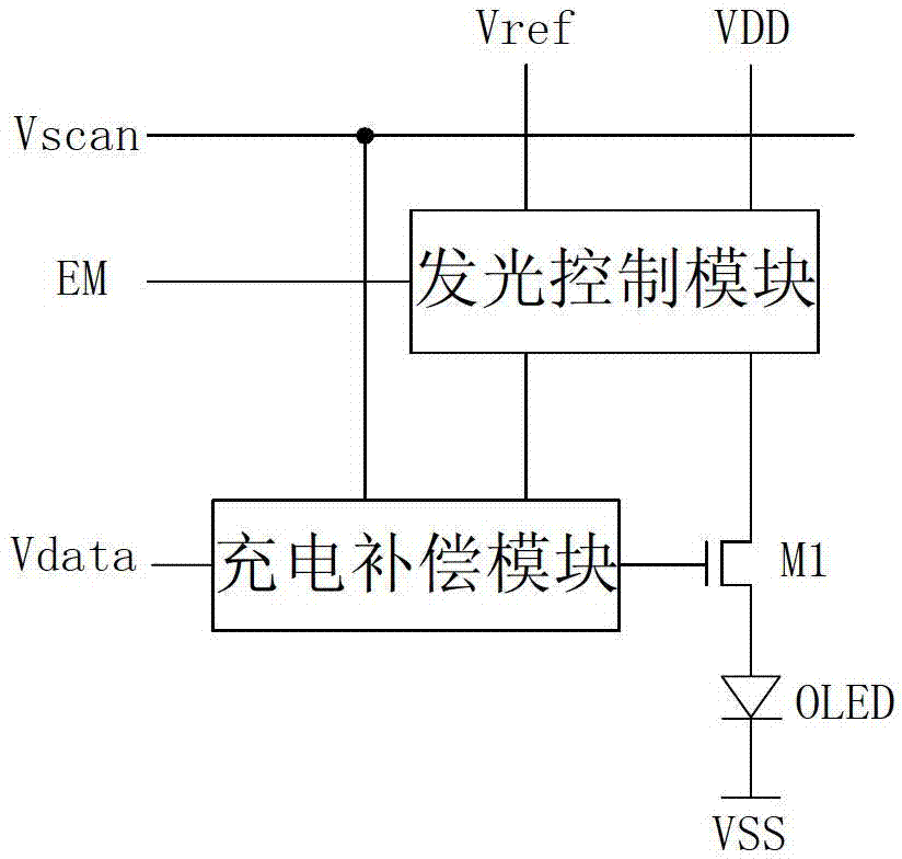
图2为本发明实施例像素驱动电路的电路图;2 is a circuit diagram of a pixel driving circuit according to an embodiment of the present invention;
图3为本发明实施例像素驱动电路的电路图之二;FIG. 3 is the second circuit diagram of the pixel driving circuit of the embodiment of the present invention;
图4为本发明实施例像素驱动电路的工作时序图;FIG. 4 is a working timing diagram of a pixel driving circuit according to an embodiment of the present invention;
图5为第一阶段本发明实施例像素驱动电路的等效电路图;5 is an equivalent circuit diagram of the pixel driving circuit of the embodiment of the present invention in the first stage;
图6为第二阶段本发明实施例像素驱动电路的等效电路图;FIG. 6 is an equivalent circuit diagram of the pixel driving circuit of the embodiment of the present invention in the second stage;
图7为发光二极管OLED额定工作电压的特征曲线图。Fig. 7 is a characteristic curve diagram of the rated operating voltage of the light emitting diode OLED.
具体实施方式Detailed ways
下面将结合本发明实施例中的附图,对本发明实施例中的技术方案进行清楚、完整地描述,显然,所描述的实施例仅仅是本发明一部分实施例,而不是全部的实施例。基于本发明中的实施例,本领域普通技术人员在没有做出创造性劳动前提下所获得的所有其他实施例,都属于本发明保护的范围。The following will clearly and completely describe the technical solutions in the embodiments of the present invention with reference to the accompanying drawings in the embodiments of the present invention. Obviously, the described embodiments are only some, not all, embodiments of the present invention. Based on the embodiments of the present invention, all other embodiments obtained by persons of ordinary skill in the art without making creative efforts belong to the protection scope of the present invention.
本发明实施例提供了一种像素驱动电路,如图2所示,包括驱动晶体管M1和有机发光二极管OLED,充电补偿模块,发光控制模块,其中,An embodiment of the present invention provides a pixel driving circuit, as shown in FIG. 2 , including a driving transistor M1, an organic light emitting diode OLED, a charge compensation module, and a light emission control module, wherein,
充电补偿模块,用于在扫描电压信号Vscan控制下,接收数据电压信号Vdata,对驱动晶体管M1进行充电,并补偿驱动晶体管M1的阈值电压;The charging compensation module is used to receive the data voltage signal Vdata under the control of the scanning voltage signal Vscan, charge the driving transistor M1, and compensate the threshold voltage of the driving transistor M1;
发光控制模块,用于在发光控制信号EM控制下,接收参考电压Vref、电源电压VDD,控制有机发光二极管发光。The light emission control module is used to receive the reference voltage Vref and the power supply voltage VDD under the control of the light emission control signal EM, and control the organic light emitting diode to emit light.
具体的,充电补偿模块,包括第二晶体管M2和第一电容C1;发光控制模块,包括第三晶体管M3和第四晶体管M4。Specifically, the charge compensation module includes a second transistor M2 and a first capacitor C1; the light emission control module includes a third transistor M3 and a fourth transistor M4.
其中,如图3所示,驱动晶体管M1用于驱动有机发光二极管OLED发光;Wherein, as shown in FIG. 3 , the driving transistor M1 is used to drive the organic light emitting diode OLED to emit light;
有机发光二极管OLED,其阳极连接驱动晶体管M1的源极,其阴极连接公共接地端电压VSS;Organic light-emitting diode OLED, its anode is connected to the source of the driving transistor M1, and its cathode is connected to the common ground terminal voltage VSS;
第一电容C1,其第一端连接驱动晶体管M1的栅极;a first capacitor C1, the first end of which is connected to the gate of the driving transistor M1;
第二晶体管M2,其栅极连接扫描电压信号Vscan,其源极连接第一电容C1的第二端,其漏极连接数据电压信号Vdata;The gate of the second transistor M2 is connected to the scanning voltage signal Vscan, its source is connected to the second end of the first capacitor C1, and its drain is connected to the data voltage signal Vdata;
第三晶体管M3,其栅极连接发光控制信号EM,其源极连接驱动晶体管M1的漏极,其漏极连接电源电压VDD;The gate of the third transistor M3 is connected to the light emission control signal EM, its source is connected to the drain of the driving transistor M1, and its drain is connected to the power supply voltage VDD;
第四晶体管M4,其栅极连接发光控制信号EM,其源极连接第一电容C1的第二端,其漏极连接参考电压Vref。The gate of the fourth transistor M4 is connected to the light emission control signal EM, the source is connected to the second terminal of the first capacitor C1, and the drain is connected to the reference voltage Vref.
上述驱动晶体管M1、第二晶体管M2、第三晶体管M3、第四晶体管M4均为N型晶体管。The driving transistor M1 , the second transistor M2 , the third transistor M3 and the fourth transistor M4 are all N-type transistors.
其中,为了方便描述,下文将第一电容C1的第一端对应的电极板称为第一电极板,将第一电容C2的第二端对应的电极板称为第二电极板。Wherein, for convenience of description, the electrode plate corresponding to the first end of the first capacitor C1 is referred to as the first electrode plate, and the electrode plate corresponding to the second end of the first capacitor C2 is referred to as the second electrode plate hereinafter.
因此,如图3所示,当扫描电压信号Vscan为高电平、发光控制信号EM为低电平时,第二晶体管M2导通、第三晶体管M3以及第四晶体管M4截止,此时第一电容C1接收数据电压信号Vdata,对驱动晶体管M1进行充电,以补偿驱动晶体管M1的阈值电压;当扫描电压信号Vscan为低电平、发光控制信号EM为高电平时,第二晶体管M2截止、第三晶体管M3以及第四晶体管M4导通,此时第一电容C1接收参考电压Vref,对驱动晶体管M1进行第二次充电,并驱动驱动晶体管M1导通,同时,电源电压VDD加载在发光二极管OLED,为发光二极管的发光提供驱动电流。需要说明的是,由于第一电容C1的电容自举效应,第一电容C1中第一电极板与第二电极板之间电势差保持不变。因此,通过电压补偿以及第二次充电拉高电压驱动过程,消除了驱动晶体管M1过驱动电压中的阈值电压,避免了阈值电压非均匀性对过驱动电压的影响。Therefore, as shown in FIG. 3, when the scanning voltage signal Vscan is at a high level and the light emission control signal EM is at a low level, the second transistor M2 is turned on, and the third transistor M3 and the fourth transistor M4 are turned off. At this time, the first capacitor C1 receives the data voltage signal Vdata, and charges the driving transistor M1 to compensate the threshold voltage of the driving transistor M1; when the scanning voltage signal Vscan is at a low level and the light emission control signal EM is at a high level, the second transistor M2 is turned off, and the third transistor M2 is turned off. The transistor M3 and the fourth transistor M4 are turned on. At this time, the first capacitor C1 receives the reference voltage Vref, charges the driving transistor M1 for the second time, and drives the driving transistor M1 to turn on. At the same time, the power supply voltage VDD is applied to the light-emitting diode OLED, Provide driving current for light emitting diode. It should be noted that due to the capacitive bootstrap effect of the first capacitor C1, the potential difference between the first electrode plate and the second electrode plate in the first capacitor C1 remains unchanged. Therefore, the threshold voltage in the overdrive voltage of the driving transistor M1 is eliminated through the voltage compensation and the second charge-up voltage driving process, and the influence of the non-uniformity of the threshold voltage on the overdrive voltage is avoided.
进一步的,如图3所示,充电补偿模块还包括:第五晶体管M5,其栅极连接扫描电压信号Vscan,源极连接第一电容C1的第一端和驱动晶体管M1的栅极,漏极连接第三晶体管M3的源极和驱动晶体管M1的漏极。当扫描电压信号Vscan为高电平、发光控制信号EM为低电平时,第五晶体管M5导通,连接了驱动晶体管M1的栅极和漏极,使得驱动晶体管M1相当于PN结,驱动晶体管M1处于饱和导通。Further, as shown in FIG. 3 , the charging compensation module further includes: a fifth transistor M5, the gate of which is connected to the scanning voltage signal Vscan, the source of which is connected to the first terminal of the first capacitor C1 and the gate of the driving transistor M1, and the drain of which is The source of the third transistor M3 is connected to the drain of the driving transistor M1. When the scanning voltage signal Vscan is at a high level and the light emission control signal EM is at a low level, the fifth transistor M5 is turned on and connected to the gate and drain of the driving transistor M1, so that the driving transistor M1 is equivalent to a PN junction, and the driving transistor M1 in saturated conduction.
下面结合具体实施例对本发明所述像素驱动电路作进一步地详细的描述说明。下列实施例中的晶体管以N型晶体管为例。The pixel driving circuit of the present invention will be further described in detail below in conjunction with specific embodiments. The transistors in the following embodiments are N-type transistors as examples.
为了方便描述,下文将驱动晶体管M1栅极对应的节点称之为G点,其漏极对应的节点称之为D点,其源极对应的节点称之为S点,第二晶体管M2源极对应的节点称之为A点。第一电容C1第一端对应的电极板称为第一电极板,将第一电容C1第二端对应的电极板称为第二电极板。For the convenience of description, the node corresponding to the gate of the driving transistor M1 is called point G, the node corresponding to the drain is called point D, the node corresponding to the source is called point S, and the source of the second transistor M2 The corresponding node is called point A. The electrode plate corresponding to the first end of the first capacitor C1 is called the first electrode plate, and the electrode plate corresponding to the second end of the first capacitor C1 is called the second electrode plate.
如图4所示,为本发明实施例像素驱动电路的工作时序图。上述像素驱动电路工作于差分输入的扫描电压信号Vscan以及发光控制信号EM下,也是说扫描电压信号Vscan以及发光控制信号EM是差分输入的。因此,当扫描电压信号Vscan处于高电平时,发光控制信号EM则处于低电平,当扫描电压信号Vscan处于低电平时,发光控制信号EM则处于高电平。As shown in FIG. 4 , it is a working timing diagram of the pixel driving circuit according to the embodiment of the present invention. The above-mentioned pixel driving circuit works under the scan voltage signal Vscan and the light emission control signal EM that are differentially input, which means that the scan voltage signal Vscan and the light emission control signal EM are differentially input. Therefore, when the scan voltage signal Vscan is at a high level, the light emission control signal EM is at a low level, and when the scan voltage signal Vscan is at a low level, the light emission control signal EM is at a high level.
在第一阶段T1时刻,扫描电压信号Vscan处于高电平、发光控制信号EM处于低电平。此时,本实施例的像素驱动电路等效电路图如图5所示,第二晶体管M2、第五晶体管M5导通,第三晶体管M3、第四晶体管M4截止,数据电压信号Vdata向第一电容C1进行补偿充电,此时VA=Vdata;与此同时,第五晶体管M5的导通使得驱动晶体管M1的漏极与栅极相连接,此时驱动晶体管M1处于饱和导通,因此驱动晶体管M1的阈值电压与栅极跟源极之间的电压差满足:Vthn=VGS=VG-VS(其中,Vthn为驱动晶体管M1的阈值电压),而节点S的电压VS=VSS+VOLED0,其中,VSS为公共接地端电压,VOLED0为有机发光二极管OLED额定工作电压。因此,驱动晶体管M1的栅极的电压VG=VS+VGS=VSS+VOLED0+Vthn。At the moment of the first stage T1, the scanning voltage signal Vscan is at a high level, and the light emission control signal EM is at a low level. At this time, the equivalent circuit diagram of the pixel driving circuit of this embodiment is shown in FIG. C1 performs compensation charging, and at this time VA=Vdata; at the same time, the conduction of the fifth transistor M5 connects the drain of the driving transistor M1 to the gate, and at this time, the driving transistor M1 is in saturated conduction, so the driving transistor M1 The threshold voltage and the voltage difference between the gate and the source satisfy: Vthn=VGS=VG-VS (wherein, Vthn is the threshold voltage of the driving transistor M1), and the voltage VS=VSS+VOLED0 of the node S, wherein, VSS is The common ground terminal voltage, VOLED0 is the rated operating voltage of the organic light emitting diode OLED. Therefore, the voltage VG of the gate of the driving transistor M1=VS+VGS=VSS+VOLED0+Vthn.
在第二阶段T2时刻,扫描电压信号Vscan处于低电平、发光控制信号EM处于高电平。此时,本实施例的像素驱动电路等效电路图如图6所示,第二晶体管M2、第五晶体管M5截止,第三晶体管M3、第四晶体管M4导通,参考电压Vref向第一电容C1进行二次充电,此时VA′=Vref。根据电容公式,C=Q/U,其中C为电容值,Q为电容两极板所带的电量,U为电容两极板之间的电压差。由于第一电容C1的自举效应,在补偿充电以及二次充电过程后,第一电容C1两极板所带电量不变,因此第一电容C1的两极板电压差保持不变,因此补偿充电以及二次充电过程使得G点的电压被拉高,此时应满足:VG′-VA′=VG-VA。而驱动晶体管M1处于导通状态,由此计算可得,此时驱动晶体管M1的栅极电压满足:VG′=Vref+(VSS+VOLED0+Vthn)-Vdata。另外,驱动晶体管M1的源极的电压满足:VS′=VSS+VOLED1。其中,VSS为公共接地端电压,VOLED1为有机发光二极管OLED正常工作过程中的工作电压。可以发现,第二阶段T2时刻加载在驱动晶体管M1上的过驱动电压满足:V过=VG′S′-Vthn=VG′-VS′-Vthn=(Vref+VSS+VOLED0+Vthn-Vdata)-(VSS+VOLED1)-Vthn,其中,Vthn为马区动晶体管M1的阈值电压。化简可得,第二阶段T2时刻加载在驱动晶体管M1上的过驱动电压满足:V过=Vref-Vdata+VOLED0-VOLED1。通过上述公式可以发现,经第一阶段T1以及第二阶段T2,此时加载在驱动晶体管M1上的过驱动电压中不再包含阈值电压Vthn。也就是说,通过第一阶段T1的补偿以及第二阶段T2的补偿充电以及二次充电驱动过程,消除了阈值电压对驱动晶体管M1过驱动电压的影响,进而使得不同像素驱动电路之间的过驱动电压变得更为一致,解决了不同像素单元之间的发光非均匀性问题,最终提高了显示装置的显示效果。At the moment of the second stage T2, the scanning voltage signal Vscan is at a low level, and the light emission control signal EM is at a high level. At this time, the equivalent circuit diagram of the pixel driving circuit of this embodiment is shown in FIG. Carry out secondary charging, at this time VA'=Vref. According to the capacitance formula, C=Q/U, where C is the capacitance value, Q is the power carried by the two plates of the capacitor, and U is the voltage difference between the two plates of the capacitor. Due to the bootstrap effect of the first capacitor C1, after the compensation charging and the second charging process, the charge on the two plates of the first capacitor C1 remains unchanged, so the voltage difference between the two plates of the first capacitor C1 remains unchanged, so the compensation charging and The voltage at point G is pulled up during the secondary charging process, which should satisfy: VG'-VA'=VG-VA. However, the driving transistor M1 is in the conduction state. From this calculation, the gate voltage of the driving transistor M1 satisfies: VG′=Vref+(VSS+VOLED0+Vthn)−Vdata. In addition, the voltage of the source of the driving transistor M1 satisfies: VS′=VSS+VOLED1 . Wherein, VSS is the voltage of the common ground terminal, and VOLED1 is the working voltage of the organic light emitting diode (OLED) during normal operation. It can be found that the overdrive voltage applied to the drive transistor M1 at the moment T2 in the second stage satisfies: Vover =VG'S'-Vthn=VG'-VS'-Vthn=(Vref+VSS+VOLED0+Vthn-Vdata)- (VSS+VOLED1)-Vthn, wherein, Vthn is the threshold voltage of the motor transistor M1. It can be simplified, and the overdrive voltage applied to the driving transistor M1 at the moment T2 in the second stage satisfies: Vover =Vref−Vdata+VOLED0−VOLED1. From the above formula, it can be found that after the first stage T1 and the second stage T2, the threshold voltage Vthn is no longer included in the overdrive voltage applied to the driving transistor M1 at this time. That is to say, through the compensation of the first stage T1, the compensation charging of the second stage T2 and the secondary charging driving process, the influence of the threshold voltage on the overdriving voltage of the driving transistor M1 is eliminated, thereby making the overdriving voltage between different pixel driving circuits The driving voltage becomes more consistent, which solves the problem of non-uniform light emission among different pixel units, and finally improves the display effect of the display device.
另外,需要特别说明的是,在后续时刻里,即在第二阶段T2时刻后的时间段内,当扫描电压信号Vscan保持低电平、发光控制信号EM保持高电平,此时第二晶体管M2、第五晶体管M5保持截止,第三晶体管M3、第四晶体管M4保持导通,参考第二阶段T2时刻计算出的驱动晶体管M1的过驱动电压公式,其中:V过=Vref-Vdata+VOLED0-VOLED1。因此保证了在后续周期中OLED发光二极管始终处于恒流控制。In addition, it needs to be specially noted that at the subsequent time, that is, in the time period after the time T2 in the second stage, when the scanning voltage signal Vscan keeps low level and the light emission control signal EM keeps high level, the second transistor M2 and the fifth transistor M5 are kept off, and the third transistor M3 and the fourth transistor M4 are kept on. Refer to the overdrive voltage formula of the driving transistor M1 calculated at the moment of the second stage T2, wherein: Vover =Vref-Vdata+VOLED0 -VOLED1. Therefore, it is ensured that the OLED light-emitting diode is always under constant current control in subsequent periods.
通过分析上述分析可以发现,第一阶段T1以及第二阶段T2构成像素驱动电路的一个显示帧周期。在第二阶段T2显示完成后,若扫描电压信号Vscan以及发光控制信号EM保持不变,该OLED发光二极管的显示状态则不发生改变。而当所述像素驱动电路再次重新开始如图4所示的工作时序时,在经历一个新的显示帧周期,即重新开始如第一阶段T1~第二阶段T2信号输入之后,新输入的数据电压Vdata会生成新的过驱动电压,进而生成一个新的发光二极管发光显示帧周期并继续后续发光显示过程。By analyzing the above analysis, it can be found that the first phase T1 and the second phase T2 constitute a display frame period of the pixel driving circuit. After the display is completed in the second stage T2, if the scan voltage signal Vscan and the light emission control signal EM remain unchanged, the display state of the OLED light emitting diode does not change. And when the pixel drive circuit restarts the working sequence as shown in FIG. 4 again, after experiencing a new display frame period, that is, after resuming signal input such as the first stage T1 to the second stage T2, the newly input data The voltage Vdata will generate a new overdrive voltage, thereby generating a new light-emitting diode display frame period and continuing the subsequent light-emitting display process.
本发明的实施例提供一种像素驱动电路,设置了充电补偿模块和发光控制模块,通过补偿驱动晶体管的阈值电压,消除了阈值电压的非均匀性问题,改善了不同像素单元之间发光非均匀性的问题,提高了像素驱动电路的驱动效果,提高了显示装置的显示效果。An embodiment of the present invention provides a pixel driving circuit, which is provided with a charge compensation module and a light emission control module. By compensating the threshold voltage of the drive transistor, the non-uniformity of the threshold voltage is eliminated, and the non-uniform light emission between different pixel units is improved. The problem of stability is improved, the driving effect of the pixel driving circuit is improved, and the display effect of the display device is improved.
此外,还需要补充说明的一点,本发明实施例提供的像素驱动电路还有下述特点。以图3所示的实施例的像素驱动电路为例,随着所述像素驱动电路的使用,OLED发光二极管会产生老化,因此OLED发光二极管所需的额定工作电压会逐渐增大,如图7所示,其横轴表示OLED发光二极管的使用时间,其纵轴表示发光二极管的额定工作电压值OLED0的大小。参考上述驱动晶体管M1的过驱动电压计算过程,像素驱动电路中驱动晶体管M1的过驱动电压满足:V过=Vref-Vdata+VOLED0-VOLED1。因此,VOLED0的增大会导致V过增大,而过驱动电压的增加会使得发光二极管的驱动电流变大,最后增加了发光二极管的发光亮度。因此,使用本发明实施例结构的像素驱动电路刚好可以弥补因OLED发光二极管长期使用老化带来的显示亮度衰减的不利效果,延长了OLED发光二极管的显示寿命。In addition, it needs to be added that the pixel driving circuit provided by the embodiment of the present invention has the following features. Taking the pixel driving circuit of the embodiment shown in FIG. 3 as an example, with the use of the pixel driving circuit, the OLED light-emitting diode will age, so the rated operating voltage required by the OLED light-emitting diode will gradually increase, as shown in FIG. 7 As shown, the horizontal axis represents the service time of the OLED light-emitting diode, and the vertical axis represents the size of the rated operating voltage OLED0 of the light-emitting diode. Referring to the above calculation process of the overdrive voltage of the drive transistor M1, the overdrive voltage of the drive transistor M1 in the pixel drive circuit satisfies: Vover =Vref−Vdata+VOLED0−VOLED1. Therefore, the increase of VOLED0 will lead to an over- increase of V, and the increase of the over-driving voltage will increase the driving current of the light-emitting diode, and finally increase the light-emitting brightness of the light-emitting diode. Therefore, the pixel driving circuit using the structure of the embodiment of the present invention can just compensate for the adverse effect of display brightness attenuation caused by long-term use and aging of the OLED light-emitting diode, and prolong the display life of the OLED light-emitting diode.
另一方面,本发明实施例提供了一种阵列基板,包括上述实施例中的像素驱动电路。其中,像素驱动电路部分同上述实施例,在此不再赘述。另外,阵列基板其他部分的结构可以参考现有技术,对此本文不再详细描述。On the other hand, an embodiment of the present invention provides an array substrate, including the pixel driving circuit in the above embodiment. Wherein, the part of the pixel driving circuit is the same as that of the above-mentioned embodiments, and will not be repeated here. In addition, the structure of other parts of the array substrate can refer to the prior art, which will not be described in detail herein.
本发明的实施例提供一种阵列基板,其中的像素驱动电路中设置了充电补偿模块和发光控制模块,通过补偿驱动晶体管的阈值电压,消除了阈值电压的非均匀性问题,改善了不同像素单元之间发光非均匀性的问题,提高了像素驱动电路的驱动效果,提高了显示装置的显示效果。An embodiment of the present invention provides an array substrate, in which a charging compensation module and a light emission control module are set in the pixel driving circuit, and by compensating the threshold voltage of the driving transistor, the problem of non-uniformity of the threshold voltage is eliminated, and the improvement of different pixel units is improved. The non-uniformity of light emission between them improves the driving effect of the pixel driving circuit and the display effect of the display device.
再一方面,本发明实施例提供了一种显示装置,包括上述实施例中的阵列基板。其中,阵列基板部分同上述实施例,在此不再赘述。另外,显示装置其他部分的结构可以参考现有技术,对此本文不再详细描述。In yet another aspect, an embodiment of the present invention provides a display device, including the array substrate in the above embodiment. Wherein, the array substrate part is the same as the above-mentioned embodiment, and will not be repeated here. In addition, the structure of other parts of the display device can refer to the prior art, which will not be described in detail herein.
本发明实施例提供的显示装置,所述显示装置可以为电脑显示器、电视显示屏、数码相框、手机、平板电脑等具有显示功能的产品或者部件,本发明不做限制。The display device provided by the embodiment of the present invention may be a computer monitor, a TV display screen, a digital photo frame, a mobile phone, a tablet computer, and other products or components with a display function, which are not limited by the present invention.
本发明的实施例提供一种显示装置,其中的像素驱动电路中设置了充电补偿模块和发光控制模块,通过补偿驱动晶体管的阈值电压,消除了阈值电压的非均匀性问题,改善了不同像素单元之间发光非均匀性的问题,提高了像素驱动电路的驱动效果,提高了显示装置的显示效果。An embodiment of the present invention provides a display device, in which a charging compensation module and a light emission control module are set in the pixel driving circuit. By compensating the threshold voltage of the driving transistor, the problem of non-uniformity of the threshold voltage is eliminated, and the improvement of different pixel units is improved. The non-uniformity of light emission between them improves the driving effect of the pixel driving circuit and the display effect of the display device.
以上所述,仅为本发明的具体实施方式,但本发明的保护范围并不局限于此,任何熟悉本技术领域的技术人员在本发明揭露的技术范围内,可轻易想到变化或替换,都应涵盖在本发明的保护范围之内。因此,本发明的保护范围应以所述权利要求的保护范围为准。The above is only a specific embodiment of the present invention, but the scope of protection of the present invention is not limited thereto. Anyone skilled in the art can easily think of changes or substitutions within the technical scope disclosed in the present invention. Should be covered within the protection scope of the present invention. Therefore, the protection scope of the present invention should be determined by the protection scope of the claims.
Claims (7)
Priority Applications (3)
| Application Number | Priority Date | Filing Date | Title |
|---|---|---|---|
| CN201310145677XA CN103236236A (en) | 2013-04-24 | 2013-04-24 | Pixel driving circuit, array substrate and display device |
| US14/342,262 US9799268B2 (en) | 2013-04-24 | 2013-06-19 | Active matrix organic light-emitting diode (AMOLED) pixel driving circuit, array substrate and display apparatus |
| PCT/CN2013/077496 WO2014172977A1 (en) | 2013-04-24 | 2013-06-19 | Pixel drive circuit, array substrate and display device |
Applications Claiming Priority (1)
| Application Number | Priority Date | Filing Date | Title |
|---|---|---|---|
| CN201310145677XA CN103236236A (en) | 2013-04-24 | 2013-04-24 | Pixel driving circuit, array substrate and display device |
Publications (1)
| Publication Number | Publication Date |
|---|---|
| CN103236236A true CN103236236A (en) | 2013-08-07 |
Family
ID=48884272
Family Applications (1)
| Application Number | Title | Priority Date | Filing Date |
|---|---|---|---|
| CN201310145677XA Pending CN103236236A (en) | 2013-04-24 | 2013-04-24 | Pixel driving circuit, array substrate and display device |
Country Status (3)
| Country | Link |
|---|---|
| US (1) | US9799268B2 (en) |
| CN (1) | CN103236236A (en) |
| WO (1) | WO2014172977A1 (en) |
Cited By (19)
| Publication number | Priority date | Publication date | Assignee | Title |
|---|---|---|---|---|
| CN104036725A (en) * | 2014-05-29 | 2014-09-10 | 京东方科技集团股份有限公司 | Pixel circuit and driving method, organic light emitting display panel and display device thereof |
| CN104658482A (en) * | 2015-03-16 | 2015-05-27 | 深圳市华星光电技术有限公司 | AMOLED (Active Matrix Organic Light Emitting Display) pixel driving circuit and method |
| WO2015096387A1 (en) * | 2013-12-26 | 2015-07-02 | 京东方科技集团股份有限公司 | Gate drive circuit, method, gate on array circuit and display apparatus |
| CN104809983A (en) * | 2015-05-07 | 2015-07-29 | 深圳市华星光电技术有限公司 | Pixel unit driving circuit, pixel unit driving method and pixel unit |
| CN106157886A (en) * | 2016-07-01 | 2016-11-23 | 友达光电股份有限公司 | Pixel circuit |
| CN106169275A (en) * | 2016-09-20 | 2016-11-30 | 武汉华星光电技术有限公司 | A kind of OLED display panel and manufacture method thereof |
| US9536476B2 (en) | 2013-12-24 | 2017-01-03 | Boe Technology Group Co., Ltd. | Gate driver circuit, gate driving method, gate-on-array circuit, display device, and electronic product |
| CN106531084A (en) * | 2017-01-05 | 2017-03-22 | 上海天马有机发光显示技术有限公司 | Organic light emitting display panel and driving method thereof, and organic light emitting display apparatus |
| US9620061B2 (en) | 2013-12-30 | 2017-04-11 | Boe Technology Group Co., Ltd. | Gate driver circuit, gate driving method, gate-on-array circuit, display device, and electronic product |
| CN110164383A (en) * | 2018-08-03 | 2019-08-23 | 上海视涯信息科技有限公司 | A kind of pixel circuit and display device |
| CN110739835A (en) * | 2018-07-18 | 2020-01-31 | 圣邦微电子(北京)股份有限公司 | Current limiting protection circuit |
| CN110782842A (en) * | 2019-11-25 | 2020-02-11 | 南京中电熊猫平板显示科技有限公司 | Self-luminous display device and in-pixel compensation circuit |
| CN110890056A (en) * | 2019-11-25 | 2020-03-17 | 南京中电熊猫平板显示科技有限公司 | A self-luminous display device and an in-pixel compensation circuit |
| WO2021027358A1 (en) * | 2019-08-15 | 2021-02-18 | 成都辰显光电有限公司 | Digital driving method for display panel and display panel |
| CN113658554A (en) * | 2021-08-17 | 2021-11-16 | 深圳市华星光电半导体显示技术有限公司 | Pixel driving circuit, pixel driving method and display device |
| CN115440161A (en) * | 2022-11-09 | 2022-12-06 | 惠科股份有限公司 | Pixel driving circuit and display panel |
| WO2023123226A1 (en) * | 2021-12-28 | 2023-07-06 | Tcl华星光电技术有限公司 | Pixel circuit and control method therefor, array substrate, and display panel |
| CN116844483A (en) * | 2023-07-24 | 2023-10-03 | 京东方科技集团股份有限公司 | Display device, display panel, pixel circuit and pixel driving method |
| CN119993068A (en) * | 2025-03-18 | 2025-05-13 | 武汉华星光电半导体显示技术有限公司 | Display panel and driving method thereof |
Families Citing this family (5)
| Publication number | Priority date | Publication date | Assignee | Title |
|---|---|---|---|---|
| KR102062875B1 (en) * | 2013-09-10 | 2020-01-07 | 삼성디스플레이 주식회사 | Pixel and organic light emitting display device using the same |
| CN105225626B (en) * | 2015-10-13 | 2018-02-02 | 上海天马有机发光显示技术有限公司 | Organic light-emitting diode pixel drive circuit, its display panel and display device |
| CN108510945B (en) * | 2018-03-06 | 2020-04-21 | 福建华佳彩有限公司 | OLED pixel compensation circuit |
| TWI697884B (en) * | 2019-08-20 | 2020-07-01 | 友達光電股份有限公司 | Pixel circuit |
| CN112582465A (en) * | 2020-12-09 | 2021-03-30 | 武汉华星光电半导体显示技术有限公司 | Thin film transistor, pixel circuit and display panel |
Citations (4)
| Publication number | Priority date | Publication date | Assignee | Title |
|---|---|---|---|---|
| EP1758084A2 (en) * | 2005-08-01 | 2007-02-28 | Samsung SDI Co., Ltd. | Data driving circuit and driving method of light emitting display using the same |
| CN101373578A (en) * | 2007-08-23 | 2009-02-25 | 三星Sdi株式会社 | Organic light emitting display and driving method thereof |
| CN102456318A (en) * | 2010-10-22 | 2012-05-16 | 乐金显示有限公司 | Organic light emitting diode display device |
| CN102968952A (en) * | 2011-08-29 | 2013-03-13 | 乐金显示有限公司 | Scan driver and organic light emitting display device using thereof |
Family Cites Families (13)
| Publication number | Priority date | Publication date | Assignee | Title |
|---|---|---|---|---|
| JP4297438B2 (en) * | 2003-11-24 | 2009-07-15 | 三星モバイルディスプレイ株式會社 | Light emitting display device, display panel, and driving method of light emitting display device |
| KR101130903B1 (en) * | 2004-08-31 | 2012-03-28 | 엘지디스플레이 주식회사 | Driving circuit of active matrix type organic light emitting diode device and method thereof |
| JP2006285116A (en) * | 2005-04-05 | 2006-10-19 | Eastman Kodak Co | Driving circuit |
| KR100624137B1 (en) * | 2005-08-22 | 2006-09-13 | 삼성에스디아이 주식회사 | Pixel circuit of organic electroluminescent display and driving method thereof |
| KR100732828B1 (en) * | 2005-11-09 | 2007-06-27 | 삼성에스디아이 주식회사 | Pixel and light emitting display device using same |
| JP5160748B2 (en) * | 2005-11-09 | 2013-03-13 | 三星ディスプレイ株式會社 | Luminescent display device |
| KR101341788B1 (en) * | 2007-07-09 | 2013-12-13 | 엘지디스플레이 주식회사 | Light lmitting display device and driving method thereof |
| KR101407302B1 (en) * | 2007-12-27 | 2014-06-13 | 엘지디스플레이 주식회사 | Light emitting display and driving method thereof |
| KR101361981B1 (en) * | 2008-02-19 | 2014-02-21 | 엘지디스플레이 주식회사 | Organic Light Emitting Diode Display And Driving Method Thereof |
| KR101058115B1 (en) * | 2009-11-16 | 2011-08-24 | 삼성모바일디스플레이주식회사 | Pixel circuit, organic electroluminescent display |
| KR101058114B1 (en) * | 2009-11-16 | 2011-08-24 | 삼성모바일디스플레이주식회사 | Pixel circuit, organic electroluminescent display |
| CN102966952A (en) | 2011-12-29 | 2013-03-13 | 马金全 | Metal honeycomb heater applied to burner of gas burning equipment and provided with same-body different-number function and manufacturing method thereof |
| CN203179476U (en) * | 2013-04-24 | 2013-09-04 | 京东方科技集团股份有限公司 | Pixel drive circuit, array substrate and display device |
-
2013
- 2013-04-24 CN CN201310145677XA patent/CN103236236A/en active Pending
- 2013-06-19 WO PCT/CN2013/077496 patent/WO2014172977A1/en not_active Ceased
- 2013-06-19 US US14/342,262 patent/US9799268B2/en active Active
Patent Citations (4)
| Publication number | Priority date | Publication date | Assignee | Title |
|---|---|---|---|---|
| EP1758084A2 (en) * | 2005-08-01 | 2007-02-28 | Samsung SDI Co., Ltd. | Data driving circuit and driving method of light emitting display using the same |
| CN101373578A (en) * | 2007-08-23 | 2009-02-25 | 三星Sdi株式会社 | Organic light emitting display and driving method thereof |
| CN102456318A (en) * | 2010-10-22 | 2012-05-16 | 乐金显示有限公司 | Organic light emitting diode display device |
| CN102968952A (en) * | 2011-08-29 | 2013-03-13 | 乐金显示有限公司 | Scan driver and organic light emitting display device using thereof |
Cited By (28)
| Publication number | Priority date | Publication date | Assignee | Title |
|---|---|---|---|---|
| US9536476B2 (en) | 2013-12-24 | 2017-01-03 | Boe Technology Group Co., Ltd. | Gate driver circuit, gate driving method, gate-on-array circuit, display device, and electronic product |
| WO2015096387A1 (en) * | 2013-12-26 | 2015-07-02 | 京东方科技集团股份有限公司 | Gate drive circuit, method, gate on array circuit and display apparatus |
| US9514683B2 (en) | 2013-12-26 | 2016-12-06 | Boe Technology Group Co., Ltd. | Gate driving circuit, gate driving method, gate on array (GOA) circuit and display device |
| US9620061B2 (en) | 2013-12-30 | 2017-04-11 | Boe Technology Group Co., Ltd. | Gate driver circuit, gate driving method, gate-on-array circuit, display device, and electronic product |
| CN104036725A (en) * | 2014-05-29 | 2014-09-10 | 京东方科技集团股份有限公司 | Pixel circuit and driving method, organic light emitting display panel and display device thereof |
| US9805654B2 (en) | 2014-05-29 | 2017-10-31 | Boe Technology Group Co., Ltd. | Pixel circuit and its driving method, organic light-emitting display panel and display device |
| CN104658482A (en) * | 2015-03-16 | 2015-05-27 | 深圳市华星光电技术有限公司 | AMOLED (Active Matrix Organic Light Emitting Display) pixel driving circuit and method |
| US9728131B2 (en) | 2015-03-16 | 2017-08-08 | Shenzhen China Star Optoelectronics Technology Co., Ltd. | Five-transistor-one-capacitor AMOLED pixel driving circuit and pixel driving method based on the circuit |
| CN104809983A (en) * | 2015-05-07 | 2015-07-29 | 深圳市华星光电技术有限公司 | Pixel unit driving circuit, pixel unit driving method and pixel unit |
| CN106157886A (en) * | 2016-07-01 | 2016-11-23 | 友达光电股份有限公司 | Pixel circuit |
| CN106169275B (en) * | 2016-09-20 | 2019-01-22 | 武汉华星光电技术有限公司 | A kind of OLED display panel and its manufacturing method |
| CN106169275A (en) * | 2016-09-20 | 2016-11-30 | 武汉华星光电技术有限公司 | A kind of OLED display panel and manufacture method thereof |
| US10460658B2 (en) | 2017-01-05 | 2019-10-29 | Shanghai Tianma AM-OLED Co., Ltd. | Organic light-emitting display panel and driving method thereof, and organic light-emitting display device |
| CN106531084A (en) * | 2017-01-05 | 2017-03-22 | 上海天马有机发光显示技术有限公司 | Organic light emitting display panel and driving method thereof, and organic light emitting display apparatus |
| CN110739835A (en) * | 2018-07-18 | 2020-01-31 | 圣邦微电子(北京)股份有限公司 | Current limiting protection circuit |
| CN110739835B (en) * | 2018-07-18 | 2021-03-05 | 圣邦微电子(北京)股份有限公司 | Current-limiting protection circuit |
| CN110164383A (en) * | 2018-08-03 | 2019-08-23 | 上海视涯信息科技有限公司 | A kind of pixel circuit and display device |
| WO2021027358A1 (en) * | 2019-08-15 | 2021-02-18 | 成都辰显光电有限公司 | Digital driving method for display panel and display panel |
| CN110782842A (en) * | 2019-11-25 | 2020-02-11 | 南京中电熊猫平板显示科技有限公司 | Self-luminous display device and in-pixel compensation circuit |
| CN110890056A (en) * | 2019-11-25 | 2020-03-17 | 南京中电熊猫平板显示科技有限公司 | A self-luminous display device and an in-pixel compensation circuit |
| CN113658554A (en) * | 2021-08-17 | 2021-11-16 | 深圳市华星光电半导体显示技术有限公司 | Pixel driving circuit, pixel driving method and display device |
| WO2023123226A1 (en) * | 2021-12-28 | 2023-07-06 | Tcl华星光电技术有限公司 | Pixel circuit and control method therefor, array substrate, and display panel |
| US12067939B2 (en) | 2021-12-28 | 2024-08-20 | Tcl China Star Optoelectronics Technology Co., Ltd. | Pixel circuit, method for controlling a pixel circuit, and array substrate |
| CN115440161A (en) * | 2022-11-09 | 2022-12-06 | 惠科股份有限公司 | Pixel driving circuit and display panel |
| CN115440161B (en) * | 2022-11-09 | 2023-03-24 | 惠科股份有限公司 | Pixel driving circuit and display panel |
| CN116844483A (en) * | 2023-07-24 | 2023-10-03 | 京东方科技集团股份有限公司 | Display device, display panel, pixel circuit and pixel driving method |
| CN119993068A (en) * | 2025-03-18 | 2025-05-13 | 武汉华星光电半导体显示技术有限公司 | Display panel and driving method thereof |
| CN119993068B (en) * | 2025-03-18 | 2026-04-14 | 武汉华星光电半导体显示技术有限公司 | Display panel and its driving method |
Also Published As
| Publication number | Publication date |
|---|---|
| WO2014172977A1 (en) | 2014-10-30 |
| US20150161944A1 (en) | 2015-06-11 |
| US9799268B2 (en) | 2017-10-24 |
Similar Documents
| Publication | Publication Date | Title |
|---|---|---|
| CN103236236A (en) | Pixel driving circuit, array substrate and display device | |
| CN103165080B (en) | Pixel circuit and driving method and display device thereof | |
| CN103198794B (en) | Image element circuit and driving method, organic electroluminescence display panel and display device | |
| CN103700342B (en) | OLED pixel circuit and driving method, display device | |
| CN104465715B (en) | Image element circuit, driving method, display panel and display device | |
| CN103218970B (en) | Active matrix organic light emitting diode (AMOLED) pixel unit, driving method and display device | |
| CN104851392B (en) | A kind of pixel-driving circuit and method, array substrate and display device | |
| CN104680980B (en) | Pixel driving circuit, driving method thereof and display device | |
| CN103117042B (en) | Pixel unit drive circuit, pixel unit drive method, pixel unit and display device | |
| CN107369413B (en) | A pixel compensation circuit, a driving method thereof, a display panel and a display device | |
| CN105139805B (en) | A kind of pixel-driving circuit and its driving method, display device | |
| US9548024B2 (en) | Pixel driving circuit, driving method thereof and display apparatus | |
| CN203179476U (en) | Pixel drive circuit, array substrate and display device | |
| CN104409047A (en) | Pixel driving circuit, pixel driving method and display device | |
| CN104036725A (en) | Pixel circuit and driving method, organic light emitting display panel and display device thereof | |
| CN104537983B (en) | Image element circuit and its driving method, display device | |
| CN104700780A (en) | Pixel circuit and driving method thereof and display device | |
| CN106067291A (en) | A kind of pixel-driving circuit and driving method, display device | |
| CN107393477B (en) | Top-emitting AMOLED pixel circuit and driving method thereof | |
| CN105427807A (en) | Pixel circuit, driving method thereof, display panel and display device | |
| CN104157241A (en) | Pixel drive circuit and drive method thereof and display device | |
| CN103366672A (en) | Light-emitting element drive circuit and pixel circuit | |
| CN104882099A (en) | Pixel drive circuit, array substrate, and display apparatus | |
| CN203858845U (en) | Pixel circuit, organic light-emitting display panel and display device | |
| CN108877679A (en) | Pixel circuit, display device and image element driving method |
Legal Events
| Date | Code | Title | Description |
|---|---|---|---|
| C06 | Publication | ||
| PB01 | Publication | ||
| C10 | Entry into substantive examination | ||
| SE01 | Entry into force of request for substantive examination | ||
| C12 | Rejection of a patent application after its publication | ||
| RJ01 | Rejection of invention patent application after publication |
Application publication date: 20130807 |