CN103473997A - Display panel, manufacturing method thereof and terminal equipment - Google Patents
Display panel, manufacturing method thereof and terminal equipment Download PDFInfo
- Publication number
- CN103473997A CN103473997A CN2013104164985A CN201310416498A CN103473997A CN 103473997 A CN103473997 A CN 103473997A CN 2013104164985 A CN2013104164985 A CN 2013104164985A CN 201310416498 A CN201310416498 A CN 201310416498A CN 103473997 A CN103473997 A CN 103473997A
- Authority
- CN
- China
- Prior art keywords
- light guide
- display panel
- substrate
- area
- light
- Prior art date
- Legal status (The legal status is an assumption and is not a legal conclusion. Google has not performed a legal analysis and makes no representation as to the accuracy of the status listed.)
- Granted
Links
- 238000004519 manufacturing process Methods 0.000 title claims abstract description 20
- 239000000758 substrate Substances 0.000 claims abstract description 76
- 238000000034 method Methods 0.000 claims description 11
- 238000010030 laminating Methods 0.000 claims 1
- 238000009434 installation Methods 0.000 description 18
- 239000000463 material Substances 0.000 description 14
- 239000011347 resin Substances 0.000 description 6
- 229920005989 resin Polymers 0.000 description 6
- 229920001187 thermosetting polymer Polymers 0.000 description 6
- 230000000007 visual effect Effects 0.000 description 5
- 230000005611 electricity Effects 0.000 description 4
- 230000001427 coherent effect Effects 0.000 description 3
- 239000004973 liquid crystal related substance Substances 0.000 description 3
- 239000011159 matrix material Substances 0.000 description 3
- 238000010586 diagram Methods 0.000 description 2
- 238000012986 modification Methods 0.000 description 2
- 230000004048 modification Effects 0.000 description 2
- 238000000059 patterning Methods 0.000 description 2
- 230000000694 effects Effects 0.000 description 1
- 238000005530 etching Methods 0.000 description 1
- 238000010438 heat treatment Methods 0.000 description 1
- 238000003754 machining Methods 0.000 description 1
- 238000000016 photochemical curing Methods 0.000 description 1
Images


Classifications
-
- G—PHYSICS
- G02—OPTICS
- G02B—OPTICAL ELEMENTS, SYSTEMS OR APPARATUS
- G02B3/00—Simple or compound lenses
- G02B3/0006—Arrays
- G02B3/0037—Arrays characterized by the distribution or form of lenses
-
- G—PHYSICS
- G02—OPTICS
- G02F—OPTICAL DEVICES OR ARRANGEMENTS FOR THE CONTROL OF LIGHT BY MODIFICATION OF THE OPTICAL PROPERTIES OF THE MEDIA OF THE ELEMENTS INVOLVED THEREIN; NON-LINEAR OPTICS; FREQUENCY-CHANGING OF LIGHT; OPTICAL LOGIC ELEMENTS; OPTICAL ANALOGUE/DIGITAL CONVERTERS
- G02F1/00—Devices or arrangements for the control of the intensity, colour, phase, polarisation or direction of light arriving from an independent light source, e.g. switching, gating or modulating; Non-linear optics
- G02F1/01—Devices or arrangements for the control of the intensity, colour, phase, polarisation or direction of light arriving from an independent light source, e.g. switching, gating or modulating; Non-linear optics for the control of the intensity, phase, polarisation or colour
- G02F1/13—Devices or arrangements for the control of the intensity, colour, phase, polarisation or direction of light arriving from an independent light source, e.g. switching, gating or modulating; Non-linear optics for the control of the intensity, phase, polarisation or colour based on liquid crystals, e.g. single liquid crystal display cells
- G02F1/133—Constructional arrangements; Operation of liquid crystal cells; Circuit arrangements
- G02F1/1333—Constructional arrangements; Manufacturing methods
- G02F1/1335—Structural association of cells with optical devices, e.g. polarisers or reflectors
- G02F1/133526—Lenses, e.g. microlenses or Fresnel lenses
-
- G—PHYSICS
- G02—OPTICS
- G02F—OPTICAL DEVICES OR ARRANGEMENTS FOR THE CONTROL OF LIGHT BY MODIFICATION OF THE OPTICAL PROPERTIES OF THE MEDIA OF THE ELEMENTS INVOLVED THEREIN; NON-LINEAR OPTICS; FREQUENCY-CHANGING OF LIGHT; OPTICAL LOGIC ELEMENTS; OPTICAL ANALOGUE/DIGITAL CONVERTERS
- G02F1/00—Devices or arrangements for the control of the intensity, colour, phase, polarisation or direction of light arriving from an independent light source, e.g. switching, gating or modulating; Non-linear optics
- G02F1/01—Devices or arrangements for the control of the intensity, colour, phase, polarisation or direction of light arriving from an independent light source, e.g. switching, gating or modulating; Non-linear optics for the control of the intensity, phase, polarisation or colour
- G02F1/13—Devices or arrangements for the control of the intensity, colour, phase, polarisation or direction of light arriving from an independent light source, e.g. switching, gating or modulating; Non-linear optics for the control of the intensity, phase, polarisation or colour based on liquid crystals, e.g. single liquid crystal display cells
- G02F1/133—Constructional arrangements; Operation of liquid crystal cells; Circuit arrangements
- G02F1/13306—Circuit arrangements or driving methods for the control of single liquid crystal cells
-
- G—PHYSICS
- G02—OPTICS
- G02F—OPTICAL DEVICES OR ARRANGEMENTS FOR THE CONTROL OF LIGHT BY MODIFICATION OF THE OPTICAL PROPERTIES OF THE MEDIA OF THE ELEMENTS INVOLVED THEREIN; NON-LINEAR OPTICS; FREQUENCY-CHANGING OF LIGHT; OPTICAL LOGIC ELEMENTS; OPTICAL ANALOGUE/DIGITAL CONVERTERS
- G02F1/00—Devices or arrangements for the control of the intensity, colour, phase, polarisation or direction of light arriving from an independent light source, e.g. switching, gating or modulating; Non-linear optics
- G02F1/01—Devices or arrangements for the control of the intensity, colour, phase, polarisation or direction of light arriving from an independent light source, e.g. switching, gating or modulating; Non-linear optics for the control of the intensity, phase, polarisation or colour
- G02F1/13—Devices or arrangements for the control of the intensity, colour, phase, polarisation or direction of light arriving from an independent light source, e.g. switching, gating or modulating; Non-linear optics for the control of the intensity, phase, polarisation or colour based on liquid crystals, e.g. single liquid crystal display cells
- G02F1/133—Constructional arrangements; Operation of liquid crystal cells; Circuit arrangements
- G02F1/1333—Constructional arrangements; Manufacturing methods
- G02F1/1335—Structural association of cells with optical devices, e.g. polarisers or reflectors
- G02F1/133509—Filters, e.g. light shielding masks
- G02F1/133512—Light shielding layers, e.g. black matrix
-
- G—PHYSICS
- G02—OPTICS
- G02F—OPTICAL DEVICES OR ARRANGEMENTS FOR THE CONTROL OF LIGHT BY MODIFICATION OF THE OPTICAL PROPERTIES OF THE MEDIA OF THE ELEMENTS INVOLVED THEREIN; NON-LINEAR OPTICS; FREQUENCY-CHANGING OF LIGHT; OPTICAL LOGIC ELEMENTS; OPTICAL ANALOGUE/DIGITAL CONVERTERS
- G02F1/00—Devices or arrangements for the control of the intensity, colour, phase, polarisation or direction of light arriving from an independent light source, e.g. switching, gating or modulating; Non-linear optics
- G02F1/01—Devices or arrangements for the control of the intensity, colour, phase, polarisation or direction of light arriving from an independent light source, e.g. switching, gating or modulating; Non-linear optics for the control of the intensity, phase, polarisation or colour
- G02F1/13—Devices or arrangements for the control of the intensity, colour, phase, polarisation or direction of light arriving from an independent light source, e.g. switching, gating or modulating; Non-linear optics for the control of the intensity, phase, polarisation or colour based on liquid crystals, e.g. single liquid crystal display cells
- G02F1/133—Constructional arrangements; Operation of liquid crystal cells; Circuit arrangements
- G02F1/1333—Constructional arrangements; Manufacturing methods
- G02F1/1335—Structural association of cells with optical devices, e.g. polarisers or reflectors
- G02F1/133509—Filters, e.g. light shielding masks
- G02F1/133514—Colour filters
-
- H—ELECTRICITY
- H10—SEMICONDUCTOR DEVICES; ELECTRIC SOLID-STATE DEVICES NOT OTHERWISE PROVIDED FOR
- H10F—INORGANIC SEMICONDUCTOR DEVICES SENSITIVE TO INFRARED RADIATION, LIGHT, ELECTROMAGNETIC RADIATION OF SHORTER WAVELENGTH OR CORPUSCULAR RADIATION
- H10F19/00—Integrated devices, or assemblies of multiple devices, comprising at least one photovoltaic cell covered by group H10F10/00, e.g. photovoltaic modules
-
- H—ELECTRICITY
- H10—SEMICONDUCTOR DEVICES; ELECTRIC SOLID-STATE DEVICES NOT OTHERWISE PROVIDED FOR
- H10F—INORGANIC SEMICONDUCTOR DEVICES SENSITIVE TO INFRARED RADIATION, LIGHT, ELECTROMAGNETIC RADIATION OF SHORTER WAVELENGTH OR CORPUSCULAR RADIATION
- H10F55/00—Radiation-sensitive semiconductor devices covered by groups H10F10/00, H10F19/00 or H10F30/00 being structurally associated with electric light sources and electrically or optically coupled thereto
-
- H—ELECTRICITY
- H10—SEMICONDUCTOR DEVICES; ELECTRIC SOLID-STATE DEVICES NOT OTHERWISE PROVIDED FOR
- H10F—INORGANIC SEMICONDUCTOR DEVICES SENSITIVE TO INFRARED RADIATION, LIGHT, ELECTROMAGNETIC RADIATION OF SHORTER WAVELENGTH OR CORPUSCULAR RADIATION
- H10F77/00—Constructional details of devices covered by this subclass
- H10F77/20—Electrodes
- H10F77/206—Electrodes for devices having potential barriers
- H10F77/211—Electrodes for devices having potential barriers for photovoltaic cells
-
- H—ELECTRICITY
- H10—SEMICONDUCTOR DEVICES; ELECTRIC SOLID-STATE DEVICES NOT OTHERWISE PROVIDED FOR
- H10F—INORGANIC SEMICONDUCTOR DEVICES SENSITIVE TO INFRARED RADIATION, LIGHT, ELECTROMAGNETIC RADIATION OF SHORTER WAVELENGTH OR CORPUSCULAR RADIATION
- H10F77/00—Constructional details of devices covered by this subclass
- H10F77/30—Coatings
- H10F77/306—Coatings for devices having potential barriers
- H10F77/311—Coatings for devices having potential barriers for photovoltaic cells
-
- H—ELECTRICITY
- H10—SEMICONDUCTOR DEVICES; ELECTRIC SOLID-STATE DEVICES NOT OTHERWISE PROVIDED FOR
- H10F—INORGANIC SEMICONDUCTOR DEVICES SENSITIVE TO INFRARED RADIATION, LIGHT, ELECTROMAGNETIC RADIATION OF SHORTER WAVELENGTH OR CORPUSCULAR RADIATION
- H10F77/00—Constructional details of devices covered by this subclass
- H10F77/40—Optical elements or arrangements
- H10F77/42—Optical elements or arrangements directly associated or integrated with photovoltaic cells, e.g. light-reflecting means or light-concentrating means
- H10F77/484—Refractive light-concentrating means, e.g. lenses
-
- H—ELECTRICITY
- H10—SEMICONDUCTOR DEVICES; ELECTRIC SOLID-STATE DEVICES NOT OTHERWISE PROVIDED FOR
- H10K—ORGANIC ELECTRIC SOLID-STATE DEVICES
- H10K59/00—Integrated devices, or assemblies of multiple devices, comprising at least one organic light-emitting element covered by group H10K50/00
- H10K59/60—OLEDs integrated with inorganic light-sensitive elements, e.g. with inorganic solar cells or inorganic photodiodes
-
- G—PHYSICS
- G02—OPTICS
- G02F—OPTICAL DEVICES OR ARRANGEMENTS FOR THE CONTROL OF LIGHT BY MODIFICATION OF THE OPTICAL PROPERTIES OF THE MEDIA OF THE ELEMENTS INVOLVED THEREIN; NON-LINEAR OPTICS; FREQUENCY-CHANGING OF LIGHT; OPTICAL LOGIC ELEMENTS; OPTICAL ANALOGUE/DIGITAL CONVERTERS
- G02F1/00—Devices or arrangements for the control of the intensity, colour, phase, polarisation or direction of light arriving from an independent light source, e.g. switching, gating or modulating; Non-linear optics
- G02F1/01—Devices or arrangements for the control of the intensity, colour, phase, polarisation or direction of light arriving from an independent light source, e.g. switching, gating or modulating; Non-linear optics for the control of the intensity, phase, polarisation or colour
- G02F1/13—Devices or arrangements for the control of the intensity, colour, phase, polarisation or direction of light arriving from an independent light source, e.g. switching, gating or modulating; Non-linear optics for the control of the intensity, phase, polarisation or colour based on liquid crystals, e.g. single liquid crystal display cells
- G02F1/133—Constructional arrangements; Operation of liquid crystal cells; Circuit arrangements
- G02F1/13306—Circuit arrangements or driving methods for the control of single liquid crystal cells
- G02F1/13324—Circuits comprising solar cells
-
- G—PHYSICS
- G02—OPTICS
- G02F—OPTICAL DEVICES OR ARRANGEMENTS FOR THE CONTROL OF LIGHT BY MODIFICATION OF THE OPTICAL PROPERTIES OF THE MEDIA OF THE ELEMENTS INVOLVED THEREIN; NON-LINEAR OPTICS; FREQUENCY-CHANGING OF LIGHT; OPTICAL LOGIC ELEMENTS; OPTICAL ANALOGUE/DIGITAL CONVERTERS
- G02F1/00—Devices or arrangements for the control of the intensity, colour, phase, polarisation or direction of light arriving from an independent light source, e.g. switching, gating or modulating; Non-linear optics
- G02F1/01—Devices or arrangements for the control of the intensity, colour, phase, polarisation or direction of light arriving from an independent light source, e.g. switching, gating or modulating; Non-linear optics for the control of the intensity, phase, polarisation or colour
- G02F1/13—Devices or arrangements for the control of the intensity, colour, phase, polarisation or direction of light arriving from an independent light source, e.g. switching, gating or modulating; Non-linear optics for the control of the intensity, phase, polarisation or colour based on liquid crystals, e.g. single liquid crystal display cells
- G02F1/133—Constructional arrangements; Operation of liquid crystal cells; Circuit arrangements
- G02F1/1333—Constructional arrangements; Manufacturing methods
- G02F1/133357—Planarisation layers
-
- Y—GENERAL TAGGING OF NEW TECHNOLOGICAL DEVELOPMENTS; GENERAL TAGGING OF CROSS-SECTIONAL TECHNOLOGIES SPANNING OVER SEVERAL SECTIONS OF THE IPC; TECHNICAL SUBJECTS COVERED BY FORMER USPC CROSS-REFERENCE ART COLLECTIONS [XRACs] AND DIGESTS
- Y02—TECHNOLOGIES OR APPLICATIONS FOR MITIGATION OR ADAPTATION AGAINST CLIMATE CHANGE
- Y02E—REDUCTION OF GREENHOUSE GAS [GHG] EMISSIONS, RELATED TO ENERGY GENERATION, TRANSMISSION OR DISTRIBUTION
- Y02E10/00—Energy generation through renewable energy sources
- Y02E10/50—Photovoltaic [PV] energy
- Y02E10/52—PV systems with concentrators
Landscapes
- Physics & Mathematics (AREA)
- Nonlinear Science (AREA)
- General Physics & Mathematics (AREA)
- Optics & Photonics (AREA)
- Chemical & Material Sciences (AREA)
- Crystallography & Structural Chemistry (AREA)
- Mathematical Physics (AREA)
- Life Sciences & Earth Sciences (AREA)
- Sustainable Development (AREA)
- Inorganic Chemistry (AREA)
- Devices For Indicating Variable Information By Combining Individual Elements (AREA)
- Engineering & Computer Science (AREA)
- Sustainable Energy (AREA)
Abstract
本发明提供所述显示面板包括相对设置的第一基板和第二基板,且第二基板的外表面包括显示区和环绕该显示区的边框区,其中,所述显示面板还包括设置在所述第二基板的外表面上的导光件,所述导光件包括第一导光件,所述第一导光件设置在所述显示区的边缘以将所述显示区边缘的光线传导至所述边框区的至少一部分的上方。本发明还提供一种包括所示显示面板的终端设备和所述显示面板的制造方法。第一导光件将显示区边缘的光线传导至边框区的至少一部分的上方。观看者观看图像时,可以看到边框区的至少一部分上方的光线形成的图像,从而可以实现窄边框显示甚至无边框显示。
According to the present invention, the display panel includes a first substrate and a second substrate oppositely arranged, and the outer surface of the second substrate includes a display area and a frame area surrounding the display area, wherein the display panel further includes a The light guide on the outer surface of the second substrate, the light guide includes a first light guide, and the first light guide is arranged on the edge of the display area to guide light from the edge of the display area to Above at least a part of the frame area. The present invention also provides a terminal device including the display panel and a manufacturing method of the display panel. The first light guide member guides light from the edge of the display area to at least a part of the frame area. When the viewer watches the image, he can see the image formed by the light above at least a part of the frame area, so that a narrow frame display or even a frameless display can be realized.
Description
技术领域technical field
本发明涉及电子设备领域,具体地,涉及一种显示面板、一种包括所述显示面板的终端设备和一种制造所述显示面板的制造方法。The present invention relates to the field of electronic equipment, and in particular, to a display panel, a terminal device including the display panel, and a manufacturing method for the display panel.
背景技术Background technique
很多电子终端设备都包括用于显示的显示面板。显示面板包括显示区和环绕该显示区的边框区。使用终端设备时,显示区显示图像和文字。终端设备包括显示面板、背光源和前框,利用前框将背光源和显示面板组合在一起,前框覆盖显示面板的边框区。边框区的存在限制了显示面板每屏所显示的画面的大小或显示的信息的量。Many electronic terminal devices include display panels for display. The display panel includes a display area and a frame area surrounding the display area. When using a terminal device, the display area displays images and text. The terminal device includes a display panel, a backlight source and a front frame. The backlight source and the display panel are combined by using the front frame, and the front frame covers the frame area of the display panel. The existence of the frame area limits the size of the picture displayed on each screen of the display panel or the amount of displayed information.
随着观看者对更好的视觉体验的追求,对窄边框甚至无边框的显示面板的需求也逐渐提高。在目前的无边框显示的终端设备中,主要通过去除前框而将显示面板直接粘贴在背光源上来实现。但是在这种结构中,显示面板和背光源之间的结合并不是十分牢固。As viewers pursue better visual experience, the demand for display panels with narrow bezels or even bezels is gradually increasing. In the current terminal equipment with borderless display, it is mainly achieved by removing the front frame and directly pasting the display panel on the backlight source. But in this structure, the combination between the display panel and the backlight is not very firm.
发明内容Contents of the invention
本发明的目的在于提供一种显示面板、一种包括该显示面板的终端设备和所述显示面板的制造方法,所述显示面板可以实现窄边框显示甚至无边框显示。The purpose of the present invention is to provide a display panel, a terminal device including the display panel, and a manufacturing method of the display panel, the display panel can realize narrow frame display or even frameless display.
为了实现上述目的,作为本发明的一个方面,提供一种显示面板,所述显示面板包括相对设置的第一基板和第二基板,且第二基板的外表面包括显示区和环绕该显示区的边框区,其中,所述显示面板还包括设置在所述第二基板的外表面上的导光件,所述导光件包括第一导光件,所述第一导光件设置在所述显示区的边缘以将从所述显示区边缘射出的光线传导至所述边框区的至少一部分的上方。In order to achieve the above object, as one aspect of the present invention, a display panel is provided, the display panel includes a first substrate and a second substrate oppositely arranged, and the outer surface of the second substrate includes a display area and a frame area, wherein the display panel further includes a light guide member disposed on the outer surface of the second substrate, the light guide member includes a first light guide member, and the first light guide member is disposed on the The edge of the display area is used to transmit the light emitted from the edge of the display area to at least a part of the frame area.
优选地,所述第一导光件为柱状件,且所述第一导光件包括安装面、折射面和连接所述安装面和所述折射面的连接面,所述安装面与所述第二基板的外表面贴合,所述显示区边缘的光线经所述第一导光件折射后从所述折射面射出,且从上至下,所述折射面上各点距离所述连接面的距离逐渐增加。Preferably, the first light guide member is a columnar member, and the first light guide member includes an installation surface, a refraction surface, and a connection surface connecting the installation surface and the refraction surface, and the installation surface is connected to the refraction surface. The outer surface of the second substrate is bonded, and the light at the edge of the display area is refracted by the first light guide and then emitted from the refraction surface, and from top to bottom, the distance between each point on the refraction surface and the connection The distance between faces increases gradually.
优选地,所述边框区包括功能部和连接部,所述功能部位于所述边框区的两端,所述连接部位于所述边框区的两侧,且连接在两端的所述功能部之间,两侧的所述连接部均对应有沿所述连接部的长度方向延伸的所述第一导光件;和/或两端的所述功能部均对应有沿所述功能部的长度方向延伸的所述第一导光件。Preferably, the frame area includes a functional part and a connecting part, the functional part is located at both ends of the frame area, the connecting part is located on both sides of the frame area, and is connected between the functional parts at both ends In between, the connecting parts on both sides correspond to the first light guide extending along the length direction of the connecting part; and/or the functional parts at both ends correspond to extending the first light guide.
优选地,所述导光件还包括设置在所述第二基板外表面上的第二导光件,所述第二导光件位于相对设置的所述第一导光件之间,且所述第二导光件和所述第一导光件的底面覆盖所述显示区,所述第二导光件对图像的放大倍数与所述第一导光件对图像的放大倍数相同。Preferably, the light guide further includes a second light guide disposed on the outer surface of the second substrate, the second light guide is located between the opposite first light guides, and the The bottom surfaces of the second light guide and the first light guide cover the display area, and the magnification of the image by the second light guide is the same as the magnification of the image by the first light guide.
优选地,所述显示面板还包括太阳能电池,所述太阳能电池设置在所述第二基板的外表面,且所述太阳能电池设置在所述第二导光件的内侧。Preferably, the display panel further includes solar cells, the solar cells are disposed on the outer surface of the second substrate, and the solar cells are disposed on the inner side of the second light guide.
优选地,所述显示面板还包括设置在所述第二基板的外表面上的平坦化层,所述平坦化层覆盖所述第二基板的外表面和所述太阳能电池,且所述平坦化层的外表面形成为平面,所述导光件形成在所述平坦化层上。Preferably, the display panel further includes a planarization layer disposed on the outer surface of the second substrate, the planarization layer covers the outer surface of the second substrate and the solar cells, and the planarization layer The outer surface of the layer is formed as a plane, and the light guide is formed on the planarization layer.
作为本发明的另一个方面,提供一种终端设备,所述终端设备包括显示面板,其中,所述显示面板为本发明所提供的上述显示面板。As another aspect of the present invention, a terminal device is provided, and the terminal device includes a display panel, wherein the display panel is the above-mentioned display panel provided by the present invention.
作为本发明的再一个方面,还提供一种显示面板的制造方法,所述显示面板包括相对设置的第一基板和第二基板,且第二基板的外表面包括显示区和环绕该显示区的边框区,其中,所述制造方法包括:As yet another aspect of the present invention, a method for manufacturing a display panel is also provided. The display panel includes a first substrate and a second substrate oppositely arranged, and the outer surface of the second substrate includes a display area and a frame surrounding the display area. A frame region, wherein the manufacturing method includes:
设置导光件,所述导光件包括第一导光件,所述第一导光件位于所述显示区的边缘以将从所述显示区边缘射出的光线传导至所述边框区的至少一部分的上方。A light guide is provided, the light guide includes a first light guide, and the first light guide is located at the edge of the display area to guide the light emitted from the edge of the display area to at least the edge of the frame area part of the top.
优选地,所述边框区包括功能部和连接部,所述功能部位于所述边框区的两端,所述连接部位于所述边框区的两侧,且连接在两端的所述功能部之间,两侧的所述连接部均对应有沿所述连接部的长度方向延伸的所述第一导光件,和/或两端的所述功能部均对应有沿所述功能部的长度方向延伸的所述第一导光件,所述导光件还包括第二导光件,所述第二导光件设置在相对设置的第一导光件之间,且所述第二导光件和所述第一导光件的底面覆盖所述显示区,所述第二导光件对图像的放大倍数与所述第一导光件对图像的放大倍数相同。Preferably, the frame area includes a functional part and a connecting part, the functional part is located at both ends of the frame area, the connecting part is located on both sides of the frame area, and is connected between the functional parts at both ends Between, the connecting parts on both sides correspond to the first light guide extending along the length direction of the connecting part, and/or the functional parts at both ends correspond to Extending the first light guide, the light guide further includes a second light guide, the second light guide is arranged between the first light guides that are oppositely arranged, and the second light guide The bottom surface of the member and the first light guide member cover the display area, and the magnification factor of the image by the second light guide member is the same as the magnification factor of the image by the first light guide member.
优选地,所述制造方法还包括在所述设置导光件的步骤之前依次进行的设置太阳能电池的步骤和形成平坦化层的步骤,所述太阳能电池设置在所述第二基板的外表面上,所述平坦化层覆盖所述第二基板的外表面和所述太阳能电池,且所述平坦化层的外表面为平面,所述导光件设置在所述平坦化层的外表面上。Preferably, the manufacturing method further includes a step of arranging a solar cell and a step of forming a planarization layer sequentially before the step of arranging the light guide, and the solar cell is arranged on the outer surface of the second substrate , the planarization layer covers the outer surface of the second substrate and the solar cell, and the outer surface of the planarization layer is a plane, and the light guide is disposed on the outer surface of the planarization layer.
显示区边缘的光线(即,显示区边缘下方的背光源发出的光线)内发出的光线传导至第一导光件,该第一导光件对显示区对应的区域内发出的光线进行折射,从而使所述光线可以被传导至边框区的至少一部分的上方。观看者观看图像时,可以看到边框区的至少一部分上方的光线形成的图像,从而可以实现窄边框显示甚至无边框显示。The light emitted from the edge of the display area (that is, the light emitted by the backlight below the edge of the display area) is transmitted to the first light guide, and the first light guide refracts the light emitted in the corresponding area of the display area, Therefore, the light can be transmitted to at least a part of the frame area. When the viewer watches the image, he can see the image formed by the light above at least a part of the frame area, so that a narrow frame display or even a frameless display can be realized.
附图说明Description of drawings
附图是用来提供对本发明的进一步理解,并且构成说明书的一部分,与下面的具体实施方式一起用于解释本发明,但并不构成对本发明的限制。在附图中:The accompanying drawings are used to provide a further understanding of the present invention, and constitute a part of the description, together with the following specific embodiments, are used to explain the present invention, but do not constitute a limitation to the present invention. In the attached picture:
图1(a)至图1(d)是展示本发明所提供的显示面板的制造方法的流程图,其中,图1(d)是本发明所提供的显示面板的剖视图;Fig. 1(a) to Fig. 1(d) are flowcharts showing the manufacturing method of the display panel provided by the present invention, wherein Fig. 1(d) is a cross-sectional view of the display panel provided by the present invention;
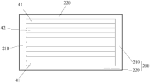
图2是本发明的显示面板的一种实施方式的俯视图;Fig. 2 is a top view of an embodiment of the display panel of the present invention;
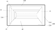
图3是本发明的显示面板的另一种实施方式的俯视图;3 is a top view of another embodiment of the display panel of the present invention;
图4是本发明所提供的显示面板的实现无边框显示的原理图;Fig. 4 is a schematic diagram of a display panel provided by the present invention for realizing borderless display;
图5是本发明所提供的显示面板上的导光件聚集光线的原理图。FIG. 5 is a schematic diagram of light collected by the light guide on the display panel provided by the present invention.
附图标记说明Explanation of reference signs
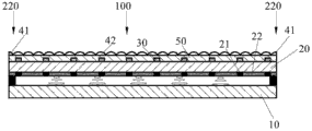
10:第一基板 20:第二基板10: The first substrate 20: The second substrate
21:黑矩阵 22:彩膜层21: Black matrix 22: Color film layer
30:太阳能电池 41:第一导光件30: Solar cell 41: The first light guide
42:第二导光件 50:平坦化层42: Second light guide 50: Planarization layer
100:显示区 200:边框区100: Display area 200: Border area
210:功能部 220:连接部210: Function Department 220: Connection Department
41a:安装面 41b:折射面41a: Mounting surface 41b: Refractive surface
41c:连接面41c: connection surface
具体实施方式Detailed ways
以下结合附图对本发明的具体实施方式进行详细说明。应当理解的是,此处所描述的具体实施方式仅用于说明和解释本发明,并不用于限制本发明。Specific embodiments of the present invention will be described in detail below in conjunction with the accompanying drawings. It should be understood that the specific embodiments described here are only used to illustrate and explain the present invention, and are not intended to limit the present invention.
如图1(d)和图2所示,作为本发明的一个方面,提供一种显示面板,该显示面板包括相对设置的第一基板10和第二基板20,第二基板20的外表面包括显示区100和环绕该显示区100的边框区200,其中,所述显示面板还包括设置在第二基板20的外表面上的导光件,该导光件包括第一导光件41,该第一导光件41设置在显示区100的边缘以将从显示区100边缘射出的光线L1传导至边框区200的至少一部分的上方。As shown in FIG. 1(d) and FIG. 2, as an aspect of the present invention, a display panel is provided, which includes a
应当理解的“第一导光件41设置在显示区100的边缘”可以理解为,第一导光件41设置在显示区100与边框区200的交界处,第一导光件41可以完全位于显示区100内,也可以一部分位于显示区100内,另一部分位于边框区200内。It should be understood that "the
如图4所示,从显示区100边缘射出的光线L1(即,显示区100边缘下方的背光源发出的光线)传导至第一导光件41,该第一导光件41对该光线L1进行折射,从而使所述光线可以被传导至边框区的至少一部分(图4中所示的是边框区的连接部220)的上方,成为出射光线L2。观看者观看图像时,可以看到边框区200的至少一部分上方的光线形成的图像。As shown in FIG. 4 , the light L1 emitted from the edge of the display area 100 (that is, the light emitted by the backlight below the edge of the display area 100 ) is transmitted to the
当第一导光件41传导的光线覆盖边框区200的一部分时,可以实现窄边框显示。当第一导光件41传导的光线完全覆盖边框区200时,可以实现无边框显示。When the light transmitted by the first
在现有的显示面板的第二基板的显示区上设置第一导光件41即可得到本发明所提供的显示面板。当将显示面板用于终端设备中时,无需省去连接显示面板和背光源的前框,从而不会降低显示面板与背光源之间的连接强度。The display panel provided by the present invention can be obtained by disposing the first
在本发明中,对第一导光件41的具体形式并没有特殊的要求,只要可以将显示区100边缘下方射出的光线L1折射至边框区200上方,以覆盖边框区200的至少一部分即可。In the present invention, there is no special requirement on the specific form of the first
为了便于设置并降低所述显示面板的总体成本,优选地,如图2中所示,第一导光件41可以为柱状件,即,第一导光件41形成为柱透镜。如图4所示,第一导光件41可以包括安装面41a、折射面41b和连接安装面41a和折射面41b的连接面41c,安装面41a与第二基板20的外表面贴合,安装面41a和折射面41b位于连接面41c的同一侧,使得显示区100边缘的光线经第一导光件41折射后从折射面41b射出,且从上至下(此处所述的“上、下”是指图4中的“上、下”方向),折射面41b上各点与连接面41c之间的距离逐渐增加。In order to facilitate installation and reduce the overall cost of the display panel, preferably, as shown in FIG. 2 , the first
将第一导光件41设置为包括安装面41a、折射面41b和连接面41c的优点在于,进入第一导光件41的光线基本上都朝同一方向发散,从而可以更好滴实现窄边框甚至无边框的显示效果。如图4中所示,连接面41c可以在于第二基板20的上表面垂直的同时与显示面板的侧面平齐。The advantage of setting the
并且,对第一导光件41的横截面形状也没有特殊要求。第一导光件41可以为四分之一圆柱,也可以为棱柱,只要可以将显示区100边缘下方发出的光线折射至边框区200上方即可。Moreover, there is no special requirement on the cross-sectional shape of the first
在本发明所提供的实施方式中,第一导光件41的横截面为四分之一圆形。此外,第一导光件41的横截面可以为直角梯形,容易理解的是,在这种情况中,第一导光件41的安装面41a大于第一导光件41的顶面。或者第一导光件41的横截面还可以为三角形。In the embodiment provided by the present invention, the cross section of the first
如图2中所示,边框区200包括功能部210和连接部220,功能部210位于边框区200的两端(图中的左右两端),连接部220位于边框区200的两侧(图中的上下两侧),且连接在两端的功能部210之间(即,功能部210和连接部220围成边框区200),第一导光件41的延伸方向平行于连接部220的延伸方向。As shown in FIG. 2 , the
在本发明中,可以只设置一个第一导光件41,该第一导光件41可以将光线折射至于该第一导光件41相邻的连接部220上方。优选地,可以设置两个第一导光件41,该两个第一导光件41的折射面41b相对设置。两个第一导光件41可以分别将光线传导至两侧的连接部220的上方。In the present invention, only one
当本发明所提供的显示面板设置在终端设备中时,将安装终端设备的功能性部件(例如,前置摄像头、听筒、话筒)的安装孔设置在功能部210中。并且,各种电路板、连接线等(例如,显示面板的驱动电路)也设置在功能部210的下方。在这种实施方式中,只需利用第一导光件41将光线引导至连接部220的上方即可。将第一导光件41的延伸方向设置为平行于连接部220的延伸方向的优点在于,可以简化第一导光件41的设置方式。优选地,两侧的连接部220均对应有沿连接部220的长度方向延伸的第一导光件41。When the display panel provided by the present invention is set in a terminal device, installation holes for installing functional components of the terminal device (for example, a front camera, an earpiece, and a microphone) are provided in the
此外,还可以将终端设备的功能性部件的安装孔设置在所述显示面板的侧面或显示面板上其他位置,此时还可以设置与两端的功能部210相对应的两个第一导光件41,从而可以实现无边框显示。In addition, the installation holes of the functional components of the terminal device can also be set on the side of the display panel or other positions on the display panel, and at this time, two first light guides corresponding to the
应当理解的是,对应于连接部220的两个第一导光件41以及对应于功能部210的两个第一导光件41首尾相接环绕显示区100的边缘设置。It should be understood that, the two first
应当理解的是,第一导光件41将显示区100边缘的光线传递至边框区200的上方之后,应当仍然能确保图像的连贯性。为了使所述显示面板显示的图像更加连贯,以使观看者获得理想的视觉效果,优选地,所述导光件还可以包括设置在第二基板20的外表面上的第二导光件42,如图2和图3所示,第二导光件42位于相对设置的第一导光件41之间,该第二导光件42对图像的放大倍数与第一导光件41对图像的放大倍数相同。It should be understood that after the first
图2中所示的是只设置有对应于连接部220的第一导光件41时,显示面板的俯视图,在这种实施方式中,第二导光件42互相平行设置。图3中所示的是设置有对应于连接部220的第一导光件41和对应于功能部210的第一导光件41时,显示面板的俯视图。在这种实施方式中,设置有平行于连接部220的第二导光件42和平行于功能部210的第二导光件42。2 is a top view of the display panel when only the first light guides 41 corresponding to the connecting
在两侧的第一导光件41之间设置第二导光件42之后,可以对整个显示区100内显示的图像的各个部分进行同等程度的放大,从而使观看者看到的图像更加连贯一致,并获得理想的视觉效果。应当理解的是,第一导光件41的底面和第二导光件42覆盖整个显示区100。容易理解的是,第二导光件42也为柱状件。After the second
在本发明中,第二导光件42的形状可以与连接面互相拼接在一起的两个第一导光件41的形状相同。例如,当第一导光件41为四分之一圆柱形时,第二导光件42可以为二分一圆柱形,当第一导光件41的横截面为直角梯形时,第二导光件42的横截面可以为等腰梯形。In the present invention, the shape of the second
为了提高利用本发明所提供的显示面板的终端设备的续航能力,优选地,所述显示面板还可以包括太阳能电池30,可以将该太阳能电池30设置在第二基板20的外表面上,从而可以通过太阳能电池30的采光面采集的太阳能进行发电,并为包括所述显示面板的终端设备供电。可以将太阳能电池30设置在第二导光件42的内侧(即,图5中的下方),一方面,太阳能电池30不会遮挡从显示区100的边缘射出的光线,另一方面,第二导光件42可以将显示面板外部的太阳光线L3聚集在太阳能电池30的采光面上,即,从显示面板外部入射的发散的太阳光线L3经第二导光件42折射后成为相对集中的入射光线L4,从而提高太阳能电池30采集的太阳能的总量(如图5所示)。In order to improve the battery life of the terminal equipment using the display panel provided by the present invention, preferably, the display panel may further include a
在本发明中,应当理解的是,在本发明中,“内”指的是,朝向显示面板内部的方向,“外”是指朝向显示面板外部的方向。太阳能电池30利用自身的采光面采集到的太阳能进行发电,从而可以为显示面板的驱动电路供电,或者可以为包括该显示面板的终端设备的电源充电,进而可以提高包括本发明所提供的显示面板的终端设备的续航能力。In the present invention, it should be understood that in the present invention, "inner" refers to a direction toward the inside of the display panel, and "outer" refers to a direction toward the outside of the display panel. The
容易理解的是,在设置有太阳能电池30的实施方式中,第二基板20的外表面上还应设置有相应的电路结构,从而可以将太阳能电池30产生的电能导出,并未所述显示装置供电。It is easy to understand that in the embodiment where the
本发明对显示面板的具体结构也没有特殊的要求,显示面板可以是液晶显示面板,也可以是有机电致发光显示面板,还可以是电致变色显示面板等。通常,如图1(d)所示,所述显示面板可以包括相对设置的第一基板10和第二基板20,太阳能电池30设置在所述第二基板20的外表面上。The present invention has no special requirements on the specific structure of the display panel, and the display panel may be a liquid crystal display panel, an organic electroluminescent display panel, or an electrochromic display panel. Generally, as shown in FIG. 1( d ), the display panel may include a
当然,太阳能电30还可以设置在第一基板10上,或者在第一基板10以及第二基板20上同时设置太阳能电池30,只要可以通过采光面采集太阳能进行发电即可。Of course, the
当所述显示面板为液晶显示面板时,第一基板10和第二基板20之间填充有液晶材料。第二基板20的内侧设置有黑矩阵21和彩膜层22,为了使显示面板具有较大的开口率,优选地,可以将太阳能电池30设置在第二基板20上与黑矩阵21相对应的位置。When the display panel is a liquid crystal display panel, liquid crystal material is filled between the
当所述显示面板为有机电致发光显示面板时,第一基板10上间隔设置有有机电致发光二极管,可以将太阳能电池30设置在第二基板20上与相邻两个有机电致发光二极管之间的间隙相对应的位置。When the display panel is an organic electroluminescent display panel, organic electroluminescent diodes are arranged at intervals on the
可以将所述导光件直接设置在太阳能电池30的外表面上,或者为了确保所述导光件牢固地固定在所述显示面板上,可以在第二基板20的外表面上设置平坦化层50,该平坦化层50覆盖太阳能电池30和第二基板20的外表面,且平坦化层50的外表面(平坦化层50与第二基板20的外表面相贴合的表面为平坦化层50的内表面,与该内表面相对的表面为平坦化层50的外表面)为平面。所述导光件设置在平坦化层50的外表面上,可以使所述导光件更加牢固地固定在显示面板中。可以利用相同的材料制造平坦化层50和所述导光件,从而可以提高所述导光件与平坦化层50之间的结合强度,防止所述导光件脱落。The light guide can be directly arranged on the outer surface of the
在所述导光件包括第二导光件42的实施方式中,由于平坦化层50的外表面为平面,因此可以使第一导光件41和第二导光件42更加均匀一致,对显示面板显示的图像的放大效果也均匀一致,从而使观看者获得更好的视觉效果。In the embodiment in which the light guide includes the second
在本发明中,对形成第一导光件41、第二导光件42和平坦化层50的具体材料并没有特殊的限定。平坦化层50只要是透明的且可以固定在第二基板20的外表面上即可,同样地,第一导光件41和第二导光件42只要是透明的且可以固定在平坦化层50的外表面上即可。In the present invention, there is no special limitation on the specific materials for forming the
例如,可以利用热固性树脂材料形成平坦化层50和/或第一导光件41和第二导光件42,或者,可以利用光固化材料形成平坦化层50和/或第一导光件41和第二导光件42。For example, the
作为本发明的另一个方面,提供一种终端设备,所述终端设备包括显示面板,其中,所述显示面板为本发明所提供的上述显示面板。As another aspect of the present invention, a terminal device is provided, and the terminal device includes a display panel, wherein the display panel is the above-mentioned display panel provided by the present invention.
如上文中所述,所述显示面板的发光面上设置有第一导光件,从而可以将显示面板的显示区的光线传导至边框区,从而可以实现窄边框显示甚至无边框显示。As mentioned above, the light-emitting surface of the display panel is provided with a first light guide member, so that the light from the display area of the display panel can be transmitted to the frame area, so that narrow frame display or even frameless display can be realized.
在包括太阳能电池的实施方式中,可以将太阳能电池与显示面板的驱动装置(例如,栅极驱动器或源极驱动器)相连,从而可以提供驱动显示面板所需的电量。In an embodiment including a solar cell, the solar cell can be connected to a driving device (for example, a gate driver or a source driver) of the display panel, so as to provide power required for driving the display panel.
或者,可以将太阳能电池直接与终端设备的电源相连,利用所述太阳能电池为所述电源充电。将太阳能电池与电源相连可以简化电路结构,易于实现。例如,直接将太阳能电池的正极与所述电源的正极相连,并直接将太阳能电池的负极与所述电源的负极相连。Alternatively, the solar cell may be directly connected to the power source of the terminal device, and the solar cell may be used to charge the power source. Connecting the solar cell to the power source can simplify the circuit structure and be easy to implement. For example, directly connect the positive pole of the solar cell to the positive pole of the power supply, and directly connect the negative pole of the solar battery to the negative pole of the power supply.
作为本发明的再一个方面,还提供一种显示面板的制造方法,如图1(a)至图1(d)和图2所示,所述显示面板包括第一基板10和第二基板20,第二基板的外表面包括显示区100和环绕该显示区100的边框区200(图2和图3),所述制造方法包括:As another aspect of the present invention, a method for manufacturing a display panel is also provided, as shown in FIG. 1(a) to FIG. 1(d) and FIG. 2 , the display panel includes a
设置导光件(如图(1d)所示),该导光件包括第一导光件41,该第一导光件41位于显示区100的边缘,以将从显示区100边缘射出的光线传导至边框区200的至少一部分的上方。A light guide is provided (as shown in FIG. Conducted to at least a portion of the
应当理解的是,所述制造方法还包括在所述设置导光件的步骤之前进行的将第一基板10和第二基板20对盒的步骤(如图1(a)所示)。It should be understood that, the manufacturing method further includes a step of aligning the
可以通过多种方式设置所述导光件,例如,可以通过构图工艺形成所述导光件,或者,可以通过卷对卷(roll to roll)转印工艺形成所述导光件。或者,可以通过机加工的方式预先制成所述导光件,随后将所述导光件粘合在显示面板的第二基板20的外表面上。The light guide can be provided in various ways, for example, the light guide can be formed by a patterning process, or the light guide can be formed by a roll-to-roll transfer process. Alternatively, the light guide may be prefabricated by machining, and then bonded to the outer surface of the
如上文中所述,为了便于加工制造并降低所述显示面板的总体成本,优选地,第一导光件41可以为柱状件。并且,在本发明中对第一导光件41的横截面形状也没有特殊限制,只要可以将显示区100边缘的光线传导至边框区200的至少一部分的上方即可。如图4所示,第一导光件41可以包括安装面41a、折射面41b和连接安装面41a和折射面41b的连接面41c,安装面41a与第二基板20的外表面贴合,安装面41a和折射面41b位于连接面41c的同一侧,使得显示区100边缘的光线经第一导光件41折射后从折射面41b射出,且从上至下(此处所述的“上、下”是指图4中的“上、下”方向),折射面41b上各点与连接面41c之间的距离逐渐增加。As mentioned above, in order to facilitate manufacturing and reduce the overall cost of the display panel, preferably, the first
将第一导光件41设置为包括安装面41a、折射面41b和连接面41c的优点在于,进入第一导光件41的光线基本上都朝同一方向发散,从而可以更好滴实现窄边框甚至无边框的显示效果。如图4中所示,连接面41c可以与显示面板的侧面平齐。The advantage of setting the
如上文中所述,如图2中所示,边框区200包括功能部210和连接部220,功能部210位于边框区200的两端(图中的左右两端),连接部220位于边框区200的两侧(图中的上下两侧),且连接在两端的功能部210之间(即,功能部210和连接部220围成边框区200),第一导光件41的延伸方向平行于连接部220的延伸方向。As mentioned above, as shown in FIG. 2 , the
或者,可以设置对应于两端的功能部210的第一导光件41,该第一导光件41平行于功能部210延伸。Alternatively, first light guides 41 corresponding to the
如图3中所示,可以同时设置平行于连接部220的第一导光件41和平行于功能部210的第一导光件41。As shown in FIG. 3 , the
上文中已经对功能部210和连接部220进行了具体描述,这里不再赘述。The
为了使所述显示面板显示的图像更加连贯,以使观看者获得理想的视觉效果,优选地,所述导光件还可以包括第二导光件42,该第二导光件42设置在相对设置的第一导光件41之间,且第二导光件42和第一导光件41的底面覆盖显示区100,第二导光件42对图像的放大倍数与第一导光件41对图像的放大倍数相同。In order to make the image displayed on the display panel more coherent, so that the viewer can obtain the ideal visual effect, preferably, the light guide can also include a second
应当理解的是,可以采用与设置第一导光件41相同的方式设置第二导光件42,并且,可以在同一步骤中同时设置第一导光件41和第二导光件42。也可以先设置第一导光件41再设置第二导光件42。It should be understood that the second
为了提高包括所述显示面板的终端设备的续航能力,优选地,所述制造方法还包括在所述设置第一导光件41的步骤之前进行的:In order to improve the battery life of the terminal device including the display panel, preferably, the manufacturing method further includes before the step of setting the first light guide 41:
设置太阳能电池30(如图1(b)所示),该太阳能电池30位于第二基板的外表面上。A solar cell 30 (as shown in FIG. 1( b )) is provided, and the
所述显示面板的第二基板20的外表面位于第二基板20的外侧,太阳能电池30形成在第二基板20的外表面上。The outer surface of the
当然,还可以将太阳能电池30设置在第一基板10上,只要可以在不影响显示面板正常显示的情况下利用采光面所采集的太阳能进行发电即可。Of course, the
为了便于设置所述导光件,优选地,所述制造方法还可以包括在所述设置太阳能电池30的步骤和所述设置导光件的步骤之间进行的形成平坦化层50的步骤,该平坦化层50覆盖第二基板20的外表面和太阳能电池30,且平坦化层50的外表面为平面,所述导光件设置在平坦化层50的外表面上。In order to facilitate the installation of the light guide member, preferably, the manufacturing method may further include a step of forming a
容易理解的是,所述设置太阳能电池30的步骤和所述形成平坦化层50的步骤是在所述设置导光件的步骤之前依次进行的。It is easy to understand that the step of arranging the
如上文中所述,可以利用热固性树脂或光固化材料制成平坦化层50。当利用热固性树脂制成平坦化层50时,可以先将热固性树脂涂布在第二基板20的外表面上,然后对第二基板20进行加热,使平坦化层50固化。当利用光固化材料制成平坦化层50时,可以先将光固化材料涂布在第二基板20的外表面上,然后利用紫外线进行照射,使光固化材料固化得到平坦化层50。As described above, the
同样地,可以利用光固化材料或热固性树脂形成第一导光件41和第二导光件42。当利用光固化材料形成第一导光件41和第二导光件42时,可先将光固化材料涂布在平坦化层50的外表面上,然后利用构图工艺对光固化材料层进行曝光,随后利用刻蚀液使光固化材料层显影,形成第一导光件41和第二导光件42。当利用热固性树脂形成第一导光件41和第二导光件42时,可以先将预成型(未固化)的第一导光件41和第二导光件42设置在平坦化层50上,随后进行加热使第一导光件41和第二导光件42固化成型并固定在平坦化层50上。Likewise, the
可以理解的是,以上实施方式仅仅是为了说明本发明的原理而采用的示例性实施方式,然而本发明并不局限于此。对于本领域内的普通技术人员而言,在不脱离本发明的精神和实质的情况下,可以做出各种变型和改进,这些变型和改进也视为本发明的保护范围。It can be understood that, the above embodiments are only exemplary embodiments adopted for illustrating the principle of the present invention, but the present invention is not limited thereto. For those skilled in the art, various modifications and improvements can be made without departing from the spirit and essence of the present invention, and these modifications and improvements are also regarded as the protection scope of the present invention.
Claims (10)
Priority Applications (3)
| Application Number | Priority Date | Filing Date | Title |
|---|---|---|---|
| CN201310416498.5A CN103473997B (en) | 2013-09-13 | 2013-09-13 | Display panel, manufacturing method thereof and terminal equipment |
| PCT/CN2014/076243 WO2015035782A1 (en) | 2013-09-13 | 2014-04-25 | Display panel, manufacturing method therefor, and terminal device |
| US14/422,808 US9618659B2 (en) | 2013-09-13 | 2014-04-25 | Display panel, manufacturing method of the same, and terminal apparatus |
Applications Claiming Priority (1)
| Application Number | Priority Date | Filing Date | Title |
|---|---|---|---|
| CN201310416498.5A CN103473997B (en) | 2013-09-13 | 2013-09-13 | Display panel, manufacturing method thereof and terminal equipment |
Publications (2)
| Publication Number | Publication Date |
|---|---|
| CN103473997A true CN103473997A (en) | 2013-12-25 |
| CN103473997B CN103473997B (en) | 2015-06-03 |
Family
ID=49798823
Family Applications (1)
| Application Number | Title | Priority Date | Filing Date |
|---|---|---|---|
| CN201310416498.5A Active CN103473997B (en) | 2013-09-13 | 2013-09-13 | Display panel, manufacturing method thereof and terminal equipment |
Country Status (3)
| Country | Link |
|---|---|
| US (1) | US9618659B2 (en) |
| CN (1) | CN103473997B (en) |
| WO (1) | WO2015035782A1 (en) |
Cited By (6)
| Publication number | Priority date | Publication date | Assignee | Title |
|---|---|---|---|---|
| WO2015035782A1 (en) * | 2013-09-13 | 2015-03-19 | 京东方科技集团股份有限公司 | Display panel, manufacturing method therefor, and terminal device |
| CN104867964A (en) * | 2015-05-18 | 2015-08-26 | 京东方科技集团股份有限公司 | Array substrate, manufacturing method thereof and organic light-emitting diode display apparatus |
| CN105336272A (en) * | 2015-11-30 | 2016-02-17 | 联想(北京)有限公司 | Electronic device |
| CN105336279A (en) * | 2014-08-14 | 2016-02-17 | 联想(北京)有限公司 | Electronic equipment |
| CN106206671A (en) * | 2016-09-05 | 2016-12-07 | 京东方科技集团股份有限公司 | The oled display substrate of integrated solar cell and display device |
| CN111864109A (en) * | 2020-07-14 | 2020-10-30 | 武汉华星光电半导体显示技术有限公司 | Display panel and display device |
Families Citing this family (3)
| Publication number | Priority date | Publication date | Assignee | Title |
|---|---|---|---|---|
| CN103970351A (en) * | 2014-04-24 | 2014-08-06 | 京东方科技集团股份有限公司 | Color film substrate, display panel and touch display device |
| CN108845623B (en) * | 2018-07-31 | 2023-11-24 | Oppo广东移动通信有限公司 | Display assembly, electronic equipment and control method of electronic equipment |
| CN113641031B (en) * | 2021-08-30 | 2022-07-01 | 厦门天马微电子有限公司 | Array substrate, display panel and display device |
Citations (6)
| Publication number | Priority date | Publication date | Assignee | Title |
|---|---|---|---|---|
| CN102184678A (en) * | 2011-05-05 | 2011-09-14 | 广东威创视讯科技股份有限公司 | Splicing display unit and large-screen display device |
| CN102540565A (en) * | 2012-03-20 | 2012-07-04 | 友达光电(苏州)有限公司 | Color filtering substrate with functions of solar battery and display panel |
| CN102879940A (en) * | 2011-07-13 | 2013-01-16 | 株式会社日本显示器西 | Display, method of manufacturing display, and electronic unit |
| US20130050613A1 (en) * | 2011-08-24 | 2013-02-28 | Panasonic Liquid Crystal Display Co., Ltd. | Liquid crystal display device |
| CN103217831A (en) * | 2013-03-29 | 2013-07-24 | 京东方科技集团股份有限公司 | Display device |
| CN103299356A (en) * | 2011-01-13 | 2013-09-11 | 夏普株式会社 | Display device |
Family Cites Families (5)
| Publication number | Priority date | Publication date | Assignee | Title |
|---|---|---|---|---|
| TWI365325B (en) * | 2008-10-31 | 2012-06-01 | Au Optronics Corp | Display apparatus |
| TWI406036B (en) * | 2010-06-28 | 2013-08-21 | Au Optronics Corp | Solar cell integrated liquid crystal display device and solar cell integrated flat display device |
| US8981391B2 (en) * | 2012-06-22 | 2015-03-17 | Industrial Technology Research Institute | Display panel with high transparency |
| US20140160387A1 (en) * | 2012-12-10 | 2014-06-12 | Hannstar Display Corporation | Liquid crystal display apparatus |
| CN103473997B (en) * | 2013-09-13 | 2015-06-03 | 北京京东方光电科技有限公司 | Display panel, manufacturing method thereof and terminal equipment |
-
2013
- 2013-09-13 CN CN201310416498.5A patent/CN103473997B/en active Active
-
2014
- 2014-04-25 US US14/422,808 patent/US9618659B2/en active Active
- 2014-04-25 WO PCT/CN2014/076243 patent/WO2015035782A1/en not_active Ceased
Patent Citations (6)
| Publication number | Priority date | Publication date | Assignee | Title |
|---|---|---|---|---|
| CN103299356A (en) * | 2011-01-13 | 2013-09-11 | 夏普株式会社 | Display device |
| CN102184678A (en) * | 2011-05-05 | 2011-09-14 | 广东威创视讯科技股份有限公司 | Splicing display unit and large-screen display device |
| CN102879940A (en) * | 2011-07-13 | 2013-01-16 | 株式会社日本显示器西 | Display, method of manufacturing display, and electronic unit |
| US20130050613A1 (en) * | 2011-08-24 | 2013-02-28 | Panasonic Liquid Crystal Display Co., Ltd. | Liquid crystal display device |
| CN102540565A (en) * | 2012-03-20 | 2012-07-04 | 友达光电(苏州)有限公司 | Color filtering substrate with functions of solar battery and display panel |
| CN103217831A (en) * | 2013-03-29 | 2013-07-24 | 京东方科技集团股份有限公司 | Display device |
Cited By (9)
| Publication number | Priority date | Publication date | Assignee | Title |
|---|---|---|---|---|
| WO2015035782A1 (en) * | 2013-09-13 | 2015-03-19 | 京东方科技集团股份有限公司 | Display panel, manufacturing method therefor, and terminal device |
| US9618659B2 (en) | 2013-09-13 | 2017-04-11 | Boe Technology Group Co., Ltd. | Display panel, manufacturing method of the same, and terminal apparatus |
| CN105336279A (en) * | 2014-08-14 | 2016-02-17 | 联想(北京)有限公司 | Electronic equipment |
| CN104867964A (en) * | 2015-05-18 | 2015-08-26 | 京东方科技集团股份有限公司 | Array substrate, manufacturing method thereof and organic light-emitting diode display apparatus |
| US10790341B2 (en) | 2015-05-18 | 2020-09-29 | Boe Technology Group Co., Ltd. | Array substrate, fabrication method thereof and organic light-emitting diode display device |
| CN105336272A (en) * | 2015-11-30 | 2016-02-17 | 联想(北京)有限公司 | Electronic device |
| CN106206671A (en) * | 2016-09-05 | 2016-12-07 | 京东方科技集团股份有限公司 | The oled display substrate of integrated solar cell and display device |
| CN106206671B (en) * | 2016-09-05 | 2019-02-26 | 京东方科技集团股份有限公司 | OLED display substrate and display device with integrated solar cell |
| CN111864109A (en) * | 2020-07-14 | 2020-10-30 | 武汉华星光电半导体显示技术有限公司 | Display panel and display device |
Also Published As
| Publication number | Publication date |
|---|---|
| US9618659B2 (en) | 2017-04-11 |
| US20160041310A1 (en) | 2016-02-11 |
| CN103473997B (en) | 2015-06-03 |
| WO2015035782A1 (en) | 2015-03-19 |
Similar Documents
| Publication | Publication Date | Title |
|---|---|---|
| CN103473997B (en) | Display panel, manufacturing method thereof and terminal equipment | |
| US8632201B2 (en) | Display device with integrated photovoltaic cells, with improved luminosity | |
| TWI479248B (en) | Electrophoretic display | |
| CN108594524A (en) | Display device | |
| RU2585312C2 (en) | High-brightness display device with integrated photovoltaic elements | |
| CN101641634B (en) | Liquid crystal display panel with microlens array and method for manufacturing the same | |
| CN104575269B (en) | Reflective display device and manufacturing method thereof | |
| US9716197B2 (en) | Backlit display device with integrated photovoltaic cells | |
| WO2017146806A1 (en) | Manufacturing display panels with integrated micro lens array | |
| CN105093681B (en) | A backlight module and a liquid crystal display device | |
| WO2012060246A1 (en) | Solar battery-equipped display device and electronic equipment | |
| CN107003554A (en) | It is integrated in the polarization photovoltaic module in electronic display device screen | |
| JP5905173B1 (en) | Liquid crystal display | |
| JP2017515168A (en) | Display device having an integrated photovoltaic cell with improved brightness and reflectivity | |
| CN103474452A (en) | Display panel and manufacturing method and terminal equipment thereof | |
| CN109976019A (en) | Transparence display plate body and transparency window having a display function | |
| US20150049424A1 (en) | Display device | |
| US20180164624A1 (en) | Splicing-type liquid crystal display device | |
| TW200629016A (en) | Electro-optical device, image printing apparatus, and method of manufacturing electro-optical device | |
| CN102413351B (en) | Three-dimensional display | |
| KR102036757B1 (en) | Flexible printed circuit board and Display device having the same | |
| JP6164411B2 (en) | Solar cell composite light emitting device and solar cell | |
| CN105116484A (en) | Light guide plate, backlight module and display device | |
| CN112394444B (en) | Light guide assembly, preparation method thereof and display device | |
| KR102106546B1 (en) | Liquid crystal display device and method for fabricating the same |
Legal Events
| Date | Code | Title | Description |
|---|---|---|---|
| C06 | Publication | ||
| PB01 | Publication | ||
| C10 | Entry into substantive examination | ||
| SE01 | Entry into force of request for substantive examination | ||
| C14 | Grant of patent or utility model | ||
| GR01 | Patent grant |