CN103682102A - Graphene field effect opto-transistor and manufacturing method thereof - Google Patents
Graphene field effect opto-transistor and manufacturing method thereof Download PDFInfo
- Publication number
- CN103682102A CN103682102A CN201310580448.0A CN201310580448A CN103682102A CN 103682102 A CN103682102 A CN 103682102A CN 201310580448 A CN201310580448 A CN 201310580448A CN 103682102 A CN103682102 A CN 103682102A
- Authority
- CN
- China
- Prior art keywords
- layer
- graphene
- quantum dot
- sio
- cdse quantum
- Prior art date
- Legal status (The legal status is an assumption and is not a legal conclusion. Google has not performed a legal analysis and makes no representation as to the accuracy of the status listed.)
- Pending
Links
Images


Classifications
-
- H—ELECTRICITY
- H10—SEMICONDUCTOR DEVICES; ELECTRIC SOLID-STATE DEVICES NOT OTHERWISE PROVIDED FOR
- H10F—INORGANIC SEMICONDUCTOR DEVICES SENSITIVE TO INFRARED RADIATION, LIGHT, ELECTROMAGNETIC RADIATION OF SHORTER WAVELENGTH OR CORPUSCULAR RADIATION
- H10F30/00—Individual radiation-sensitive semiconductor devices in which radiation controls the flow of current through the devices, e.g. photodetectors
- H10F30/20—Individual radiation-sensitive semiconductor devices in which radiation controls the flow of current through the devices, e.g. photodetectors the devices having potential barriers, e.g. phototransistors
- H10F30/21—Individual radiation-sensitive semiconductor devices in which radiation controls the flow of current through the devices, e.g. photodetectors the devices having potential barriers, e.g. phototransistors the devices being sensitive to infrared, visible or ultraviolet radiation
- H10F30/28—Individual radiation-sensitive semiconductor devices in which radiation controls the flow of current through the devices, e.g. photodetectors the devices having potential barriers, e.g. phototransistors the devices being sensitive to infrared, visible or ultraviolet radiation the devices being characterised by field-effect operation, e.g. junction field-effect phototransistors
- H10F30/287—Individual radiation-sensitive semiconductor devices in which radiation controls the flow of current through the devices, e.g. photodetectors the devices having potential barriers, e.g. phototransistors the devices being sensitive to infrared, visible or ultraviolet radiation the devices being characterised by field-effect operation, e.g. junction field-effect phototransistors the devices having PN heterojunction gates
- H10F30/2877—Field-effect phototransistors having PN heterojunction gates
-
- H—ELECTRICITY
- H10—SEMICONDUCTOR DEVICES; ELECTRIC SOLID-STATE DEVICES NOT OTHERWISE PROVIDED FOR
- H10F—INORGANIC SEMICONDUCTOR DEVICES SENSITIVE TO INFRARED RADIATION, LIGHT, ELECTROMAGNETIC RADIATION OF SHORTER WAVELENGTH OR CORPUSCULAR RADIATION
- H10F71/00—Manufacture or treatment of devices covered by this subclass
- H10F71/121—The active layers comprising only Group IV materials
-
- H—ELECTRICITY
- H10—SEMICONDUCTOR DEVICES; ELECTRIC SOLID-STATE DEVICES NOT OTHERWISE PROVIDED FOR
- H10F—INORGANIC SEMICONDUCTOR DEVICES SENSITIVE TO INFRARED RADIATION, LIGHT, ELECTROMAGNETIC RADIATION OF SHORTER WAVELENGTH OR CORPUSCULAR RADIATION
- H10F77/00—Constructional details of devices covered by this subclass
- H10F77/10—Semiconductor bodies
- H10F77/14—Shape of semiconductor bodies; Shapes, relative sizes or dispositions of semiconductor regions within semiconductor bodies
- H10F77/143—Shape of semiconductor bodies; Shapes, relative sizes or dispositions of semiconductor regions within semiconductor bodies comprising quantum structures
- H10F77/1433—Quantum dots
-
- Y—GENERAL TAGGING OF NEW TECHNOLOGICAL DEVELOPMENTS; GENERAL TAGGING OF CROSS-SECTIONAL TECHNOLOGIES SPANNING OVER SEVERAL SECTIONS OF THE IPC; TECHNICAL SUBJECTS COVERED BY FORMER USPC CROSS-REFERENCE ART COLLECTIONS [XRACs] AND DIGESTS
- Y02—TECHNOLOGIES OR APPLICATIONS FOR MITIGATION OR ADAPTATION AGAINST CLIMATE CHANGE
- Y02P—CLIMATE CHANGE MITIGATION TECHNOLOGIES IN THE PRODUCTION OR PROCESSING OF GOODS
- Y02P70/00—Climate change mitigation technologies in the production process for final industrial or consumer products
- Y02P70/50—Manufacturing or production processes characterised by the final manufactured product
Landscapes
- Thin Film Transistor (AREA)
Abstract
本发明公开的石墨烯场效应光晶体管自下而上依次有Si层和SiO2层的Si/SiO2复合晶片、n层石墨烯层,n=1-2、两块在同一水平面上彼此相隔的金电极、在两块金电极之间有CdSe量子点层,CdSe量子点层中的CdSe量子点的直径为3-8nm。其制造步骤包括:将用胶带从石墨烯晶体上剥离的石墨烯层黏贴到清洗干净的Si/SiO2复合晶片上;在石墨烯层上旋涂聚甲基丙烯酸甲酯,用电子束曝光法在涂层上刻蚀出金电极;用电子束蒸发方法在电极上依次沉积Ni和Au作为源极和漏极,制备CdSe量子点溶液;将CdSe量子点溶液涂覆到二块金电极之间的石墨烯层上。本发明为场效应光晶体管提供了一种新品种。
The graphene field effect phototransistor disclosed by the present invention has Si layer and SiO 2 layer Si/SiO 2 composite wafer, n-layer graphene layer, n=1-2, two blocks are separated from each other on the same horizontal plane successively from bottom to top A gold electrode, a CdSe quantum dot layer is arranged between two gold electrodes, and the diameter of the CdSe quantum dot in the CdSe quantum dot layer is 3-8nm. Its manufacturing steps include: adhering the graphene layer peeled from the graphene crystal with adhesive tape to the cleaned Si/ SiO2 composite wafer; spin-coating polymethyl methacrylate on the graphene layer, exposing it with an electron beam The gold electrode is etched on the coating by the method; the electron beam evaporation method is used to deposit Ni and Au on the electrode as the source and the drain in turn to prepare the CdSe quantum dot solution; the CdSe quantum dot solution is coated on the two gold electrodes on the graphene layer between them. The invention provides a new type of field effect phototransistor.
Description
技术领域 technical field
本发明涉及一种场效应光晶体管及其制造方法,尤其是石墨烯场效应光晶体管及其制造方法。 The invention relates to a field-effect phototransistor and a manufacturing method thereof, in particular to a graphene field-effect phototransistor and a manufacturing method thereof.
背景技术 Background technique
光晶体管是由双极型晶体管或场效应晶体管等三端器件构成的光电器件。光在这类器件的有源区内被吸收,产生光生载流子,通过内部电放大机构,产生光电流增益,光晶体管三端工作,故容易实现电控或电同步。光晶体管所用材料通常是砷化镓(CaAs),主要分为双极型光晶体管、场效应光晶体管及其相关器件。双极型光晶体管通常增益很高,对于GaAs-GaAlAs,放大系数可大于1000,响应时间大于纳秒,常用于光探测器,也可用于光放大。场效应光晶体管响应速度快(约为50皮秒),常用作极高速光探测器。与此相关还有许多其他平面型光电器件,其特点均是速度快(响应时间几十皮秒)、适于集成。 A phototransistor is an optoelectronic device composed of a three-terminal device such as a bipolar transistor or a field effect transistor. Light is absorbed in the active region of this type of device to generate photogenerated carriers, which generate photocurrent gain through the internal electrical amplification mechanism, and the phototransistor works at three terminals, so it is easy to realize electrical control or electrical synchronization. The material used in phototransistors is usually gallium arsenide (CaAs), which is mainly divided into bipolar phototransistors, field effect phototransistors and related devices. Bipolar phototransistors usually have high gain. For GaAs-GaAlAs, the amplification factor can be greater than 1000, and the response time is greater than nanoseconds. It is often used in photodetectors and can also be used for optical amplification. Field-effect phototransistors have fast response times (approximately 50 picoseconds) and are often used as extremely high-speed photodetectors. Related to this, there are many other planar optoelectronic devices, which are characterized by fast speed (response time tens of picoseconds) and suitable for integration.
目前,在光探测领域最新的研究成果是基于量子点调控的光晶体管。这种光晶体管可以提供比较高的光增益,并且有比较小的暗电流。据报道,有铝掺杂的氧化锌(AZO)和PbS量子点的光晶体管混合结构对红外光的吸收强烈,可以用于红外波段光电探测器的制作;基于石墨烯-PbS量子点混合而得到的光电MOS管,具有108电子/光子的量子效率和107A/W的高灵敏度,最低可探测10-15 W的光强;而单壁碳纳米管与量子点的混合光晶体管结构增强了光的斯塔效应。对量子点混合结构光晶体管的研究具有重要意义。 At present, the latest research achievement in the field of light detection is based on the phototransistor regulated by quantum dots. This phototransistor can provide relatively high optical gain and has relatively small dark current. According to reports, the phototransistor hybrid structure of aluminum-doped zinc oxide (AZO) and PbS quantum dots has a strong absorption of infrared light and can be used for the production of photodetectors in the infrared band; based on graphene-PbS quantum dots mixed to obtain The photoelectric MOS tube has a quantum efficiency of 10 8 electrons/photons and a high sensitivity of 10 7 A/W, and can detect a light intensity of 10 -15 W at the lowest; while the hybrid phototransistor structure of single-walled carbon nanotubes and quantum dots enhances The Star effect of light. The research on quantum dot hybrid structured phototransistor is of great significance.
发明内容 Contents of the invention
本发明的目的是为光探测领域提供一种使用半导体材料石墨烯而构建的场效应晶体管其制造方法,为场效应光晶体管提供一种新品种。 The purpose of the present invention is to provide a method for manufacturing a field-effect transistor constructed by using semiconductor material graphene in the field of light detection, and to provide a new type of field-effect phototransistor.
本发明的石墨烯场效应光晶体管,自下而上依次有Si层和SiO2层的Si/SiO2复合晶片、n层石墨烯层,n=1-2、两块在同一水平面上彼此相隔的金电极、在两块金电极之间有CdSe量子点层,CdSe量子点层中的CdSe量子点的直径为3-8nm。 Graphene field-effect phototransistor of the present invention has Si layer and SiO2 layer Si/ SiO2 composite wafer, n-layer graphene layer successively from bottom to top, n=1-2, two pieces are separated from each other on the same horizontal plane A gold electrode, a CdSe quantum dot layer is arranged between two gold electrodes, and the diameter of the CdSe quantum dot in the CdSe quantum dot layer is 3-8nm.
通常,Si/SiO2复合晶片的SiO2层的厚度为30-300nm,Si层厚度为200μm。CdSe量子点层的厚度为10-600nm。 Usually, the thickness of SiO2 layer of Si/ SiO2 composite wafer is 30-300nm, and the thickness of Si layer is 200μm. The thickness of the CdSe quantum dot layer is 10-600nm.
本发明的石墨烯场效应光晶体管的制造方法,包括如下步骤: The manufacture method of graphene field-effect phototransistor of the present invention, comprises the steps:
1)使用微机械力方法,用胶带从石墨烯晶体上剥离n层石墨烯,n=1-2,再将石墨烯黏贴到清洗干净的Si/SiO2复合晶片的SiO2层上; 1) Using micromechanical force method, peel off n layers of graphene from the graphene crystal with adhesive tape, n=1-2, and then paste the graphene on the SiO 2 layer of the cleaned Si/SiO 2 composite wafer;
2)在石墨烯层上旋涂质量浓度1%-10%的聚甲基丙烯酸甲酯,采用电子束曝光法在聚甲基丙烯酸甲酯涂层上刻蚀出金电极图形; 2) Spin-coat polymethyl methacrylate with a mass concentration of 1%-10% on the graphene layer, and etch gold electrode patterns on the polymethyl methacrylate coating by electron beam exposure;
3)采用电子束蒸发方法,在刻蚀的金电极图形上依次沉积5nmNi和20-100nmAu,作为场效应光晶体管的源极和漏极; 3) Using the electron beam evaporation method, sequentially deposit 5nmNi and 20-100nmAu on the etched gold electrode pattern, as the source and drain of the field effect phototransistor;
4)将丙烯酸羟丙酯充分溶解于氧化三辛基膦中,得到氧化三辛基膦丙烯酸羟丙酯混合溶液,混合溶液中丙烯酸羟丙酯的质量浓度为8%;将Se、Cd(CH3)2和三丁基膦按质量比1:2:38混合,得到储备液,将0.5-2ml储备液倒入加热至360℃的2-4g上述氧化三辛基膦丙烯酸羟丙酯混合溶液中,保持360℃温度不变,反应0.1-1小时,自然冷却至室温,得到CdSe量子点溶液; 4) Fully dissolve hydroxypropyl acrylate in trioctylphosphine oxide to obtain a mixed solution of trioctylphosphine oxide hydroxypropyl acrylate, the mass concentration of hydroxypropyl acrylate in the mixed solution is 8%; Se, Cd(CH 3 ) 2 and tributylphosphine were mixed at a mass ratio of 1:2:38 to obtain a stock solution, and 0.5-2ml stock solution was poured into 2-4g of the above-mentioned trioctylphosphine oxide hydroxypropyl acrylate mixed solution heated to 360°C , keeping the temperature at 360°C constant, reacting for 0.1-1 hour, and naturally cooling to room temperature to obtain a CdSe quantum dot solution;
5)采用旋涂的方法将步骤4)制得的CdSe量子点溶液涂覆到二块金电极之间的石墨烯层上,得到石墨烯场效应光晶体管。 5) Coating the CdSe quantum dot solution prepared in step 4) onto the graphene layer between the two gold electrodes by spin coating to obtain a graphene field effect phototransistor.
本发明制备过程中,清洗Si/SiO2复合晶片可以是先依次用去离子水、丙酮和异丙醇清洗,然后再用O2:Ar=1:1的混合等离子气体清洗。 In the preparation process of the present invention, cleaning the Si/SiO 2 composite wafer may be performed by first cleaning with deionized water, acetone and isopropanol in sequence, and then cleaning with a mixed plasma gas of O 2 : Ar=1:1.
上述步骤2)的电子束曝光刻蚀的曝光时间为1-2s、显影时间40s-1min。步骤3)的电子束蒸发过程中,气压控制在5×10⁻³Pa以下。 The exposure time of the electron beam exposure etching in the above step 2) is 1-2s, and the developing time is 40s-1min. During the electron beam evaporation process in step 3), the air pressure is controlled below 5×10 -3 Pa.
石墨烯具有二维晶体结构,表面平整,在室温下传递电子的速度比已知导体都快。利用石墨烯和CdSe量子点混合,可以克服石墨烯光透明的缺点,制造出石墨烯场效应晶体管结构。 Graphene has a two-dimensional crystal structure with a flat surface and can transfer electrons faster than any known conductor at room temperature. By using the mixture of graphene and CdSe quantum dots, the shortcomings of graphene's light transparency can be overcome, and a graphene field effect transistor structure can be manufactured.
本发明的石墨烯场效应光晶体管中石墨烯层受到Si背栅电极的调控,利用光致激发CdSe量子点构建成石墨烯的场效应晶体管。本发明为场效应光晶体管提供了一种新品种。 In the graphene field effect phototransistor of the present invention, the graphene layer is regulated by the Si back gate electrode, and the graphene field effect transistor is constructed by using photoinduced excitation of CdSe quantum dots. The invention provides a new type of field effect phototransistor.
附图说明 Description of drawings
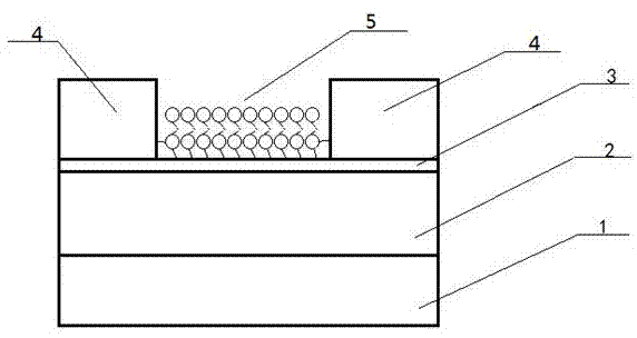
图1为石墨烯场效应光晶体管的结构示意图; Fig. 1 is the structural representation of graphene field-effect phototransistor;
图2为石墨烯场效应光晶体管的俯视图; Fig. 2 is the top view of graphene field-effect phototransistor;
图3为石墨烯场效应晶体管栅极电压与漏极电流的关系; Fig. 3 is the relation of graphene field effect transistor gate voltage and drain current;
图4为石墨烯场效应晶体管在不同栅压下漏极电流与漏极电压的关系。 Fig. 4 is the relationship between the drain current and the drain voltage of the graphene field effect transistor under different gate voltages.
具体实施方式 Detailed ways
以下结合附图进一步说明本发明。 Further illustrate the present invention below in conjunction with accompanying drawing.
参照图1、图2,本发明的石墨烯场效应光晶体管自下而上依次有Si层1和SiO2层2的Si/SiO2复合晶片、n层石墨烯层3,n=1-2、两块在同一水平面上彼此相隔的金电极4、在两块金电极4之间有CdSe量子点层5,CdSe量子点层5中的CdSe量子点的直径为3-8nm。
With reference to Fig. 1, Fig. 2, graphene field-effect phototransistor of the present invention has Si layer 1 and SiO 2 layer 2 Si/SiO Composite wafer, n-layer graphene layer 3 successively from bottom to top, n=1-2 1. Two
实施例1: Example 1:
1)将Si/SiO2复合晶片依次用去离子水、丙酮和异丙醇清洗,然后再用O2:Ar=1:1的混合等离子气体清洗;用胶带从石墨烯晶体上剥离单层石墨烯黏贴到清洗干净的Si/SiO2晶片的SiO2层上,其中SiO2层厚度250nm; 1) Clean the Si/SiO 2 composite wafer with deionized water, acetone and isopropanol in sequence, and then clean it with a mixed plasma gas of O 2 : Ar=1:1; use tape to peel off the single-layer graphite from the graphene crystal olefin is pasted on the SiO 2 layer of the cleaned Si/SiO 2 wafer, wherein the thickness of the SiO 2 layer is 250nm;
2)在石墨烯上旋涂质量浓度10%的聚甲基丙烯酸甲酯(PMMA),采用电子束曝光法在聚甲基丙烯酸甲酯涂层上刻蚀出金电极图形,电子束曝光刻蚀的曝光时间为2s、显影时间40s; 2) Spin-coat polymethyl methacrylate (PMMA) with a mass concentration of 10% on the graphene, etch the gold electrode pattern on the PMMA coating by electron beam exposure, and then etch The exposure time is 2s and the developing time is 40s;
3)采用电子束蒸发方法,在刻蚀的金电极图形上依次沉积5nmNi和20nmAu,电子束蒸发过程中,气压控制在5×10⁻³Pa; 3) Using electron beam evaporation method, sequentially deposit 5nmNi and 20nmAu on the etched gold electrode pattern. During the electron beam evaporation process, the air pressure is controlled at 5×10 -3 Pa;
4)将丙烯酸羟丙酯充分溶解于氧化三辛基膦中,得到氧化三辛基膦丙烯酸羟丙酯混合溶液,混合溶液中丙烯酸羟丙酯的质量浓度为8%;将Se、Cd(CH3)2和三丁基膦按质量比1:2:38混合,得到储备液,将1ml储备液倒入加热至360℃的3g上述氧化三辛基膦丙烯酸羟丙酯混合溶液中,保持360℃温度不变,反应0.3小时,自然冷却至室温,得到CdSe量子点液,CdSe量子点直径为5nm; 4) Fully dissolve hydroxypropyl acrylate in trioctylphosphine oxide to obtain a mixed solution of trioctylphosphine oxide hydroxypropyl acrylate, the mass concentration of hydroxypropyl acrylate in the mixed solution is 8%; Se, Cd(CH 3 ) 2 and tributylphosphine were mixed at a mass ratio of 1:2:38 to obtain a stock solution, and 1ml of stock solution was poured into 3g of the above mixed solution of trioctylphosphine oxide hydroxypropyl acrylate heated to 360°C, and kept at 360 Keep the temperature constant at ℃, react for 0.3 hours, cool naturally to room temperature, and obtain CdSe quantum dot liquid, the diameter of CdSe quantum dots is 5nm;
5)采用旋涂的方法将步骤4)制得的CdSe量子点层涂覆到二块金电极之间的单层石墨烯上,CdSe量子点层涂覆厚550nm,得到石墨烯场效应光晶体管。 5) Coat the CdSe quantum dot layer prepared in step 4) on the single-layer graphene between the two gold electrodes by spin coating, and the CdSe quantum dot layer is coated with a thickness of 550nm to obtain a graphene field effect phototransistor .
本例的石墨烯场效应晶体管在波长532nm(Nd3+YAG倍频激光器)功率1.7pw的绿色激光激发下栅极电压与漏极电流的关系见图3。不同栅压下漏极电流与漏极电压的关系见图4。 The relationship between the gate voltage and the drain current of the graphene field effect transistor in this example under the excitation of a green laser with a wavelength of 532nm (Nd 3 +YAG frequency doubling laser) and a power of 1.7pw is shown in Figure 3. The relationship between drain current and drain voltage under different gate voltages is shown in Figure 4.
the
实施例2: Example 2:
1)将Si/SiO2复合晶片依次用去离子水、丙酮和异丙醇清洗,然后再用O2:Ar=1:1的混合等离子气体清洗;用胶带从石墨烯晶体上剥离双层石墨烯黏贴到清洗干净的Si/SiO2晶片的SiO2层上,其中SiO2层厚度300nm; 1) Clean the Si/SiO 2 composite wafer with deionized water, acetone and isopropanol in sequence, and then clean it with a mixed plasma gas of O 2 : Ar=1:1; use adhesive tape to peel off the double-layer graphite from the graphene crystal olefin is pasted on the SiO 2 layer of the cleaned Si/SiO 2 wafer, wherein the thickness of the SiO 2 layer is 300nm;
2)在三层石墨烯上旋涂质量浓度1%的PMMA,采用电子束曝光法在聚甲基丙烯酸甲酯涂层上刻蚀出金电极图形,电子束曝光刻蚀的曝光时间为1s、显影时间1min; 2) Spin-coat PMMA with a mass concentration of 1% on the three-layer graphene, and use the electron beam exposure method to etch the gold electrode pattern on the polymethyl methacrylate coating. The exposure time of the electron beam exposure etching is 1s, Development time 1min;
3)采用电子束蒸发方法,在刻蚀的金电极图形上依次沉积5nmNi和80nmAu,电子束蒸发过程中,气压控制在5×10⁻³Pa; 3) Using electron beam evaporation method, sequentially deposit 5nmNi and 80nmAu on the etched gold electrode pattern. During the electron beam evaporation process, the air pressure is controlled at 5×10 -3 Pa;
4)将丙烯酸羟丙酯充分溶解于氧化三辛基膦中,得到氧化三辛基膦丙烯酸羟丙酯混合溶液,混合溶液中丙烯酸羟丙酯的质量浓度为8%;将Se、Cd(CH3)2和三丁基膦按质量比1:2:38混合,得到储备液,将2ml储备液倒入加热至360℃的2g上述氧化三辛基膦丙烯酸羟丙酯混合溶液中,保持360℃温度不变,反应0.8小时,自然冷却至室温,得到CdSe量子点溶液,CdSe量子点直径为8nm; 4) Fully dissolve hydroxypropyl acrylate in trioctylphosphine oxide to obtain a mixed solution of trioctylphosphine oxide hydroxypropyl acrylate, the mass concentration of hydroxypropyl acrylate in the mixed solution is 8%; Se, Cd(CH 3 ) 2 and tributylphosphine were mixed at a mass ratio of 1:2:38 to obtain a stock solution, and 2ml of the stock solution was poured into 2g of the above-mentioned trioctylphosphine oxide hydroxypropyl acrylate mixed solution heated to 360°C, and kept at 360 Keep the temperature constant at ℃, react for 0.8 hours, and cool naturally to room temperature to obtain a CdSe quantum dot solution, the diameter of the CdSe quantum dot is 8nm;
5)采用旋涂的方法将步骤4)制得的CdSe量子点层涂覆在二块金电极之间的四层石墨烯上,CdSe量子点层涂覆厚400nm,得到石墨烯场效应光晶体管。 5) Coat the CdSe quantum dot layer prepared in step 4) on the four-layer graphene between the two gold electrodes by spin coating, and the CdSe quantum dot layer is coated with a thickness of 400nm to obtain a graphene field effect phototransistor .
实施例3: Example 3:
1)将Si/SiO2复合晶片依次用去离子水、丙酮和异丙醇清洗,然后再用O2:Ar=1:1的混合等离子气体清洗;用胶带从石墨烯晶体上剥离单层石墨烯黏贴到清洗干净的Si/SiO2晶片的SiO2层上,其中SiO2层厚度280nm; 1) Clean the Si/SiO 2 composite wafer with deionized water, acetone and isopropanol in sequence, and then clean it with a mixed plasma gas of O 2 : Ar=1:1; use tape to peel off the single-layer graphite from the graphene crystal olefin is pasted on the SiO 2 layer of the cleaned Si/SiO 2 wafer, wherein the thickness of the SiO 2 layer is 280nm;
2)在石墨烯层上旋涂质量浓度5%的PMMA,采用电子束曝光法在聚甲基丙烯酸甲酯涂层上刻蚀出金电极图形,电子束曝光刻蚀的曝光时间为2s、显影时间50s; 2) Spin-coat PMMA with a mass concentration of 5% on the graphene layer, and etch the gold electrode pattern on the polymethyl methacrylate coating by electron beam exposure. The exposure time of electron beam exposure etching is 2s, and the developing time 50s;
3)采用电子束蒸发方法,在刻蚀的金电极图形上依次沉积5nmNi和40nmAu,电子束蒸发过程中,气压控制在5×10⁻³Pa; 3) Using electron beam evaporation method, sequentially deposit 5nmNi and 40nmAu on the etched gold electrode pattern. During the electron beam evaporation process, the air pressure is controlled at 5×10 -3 Pa;
4)将丙烯酸羟丙酯充分溶解于氧化三辛基膦中,得到氧化三辛基膦丙烯酸羟丙酯混合溶液,混合溶液中丙烯酸羟丙酯的质量浓度为8%;将Se、Cd(CH3)2和三丁基膦按质量比1:2:38混合,得到储备液,将0.5ml储备液倒入加热至360℃的1g上述氧化三辛基膦丙烯酸羟丙酯混合溶液中,保持360℃温度不变,反应1小时,自然冷却至室温,得到CdSe量子点液,CdSe量子点直径为3nm; 4) Fully dissolve hydroxypropyl acrylate in trioctylphosphine oxide to obtain a mixed solution of trioctylphosphine oxide hydroxypropyl acrylate, the mass concentration of hydroxypropyl acrylate in the mixed solution is 8%; Se, Cd(CH 3 ) 2 and tributylphosphine were mixed at a mass ratio of 1:2:38 to obtain a stock solution, and 0.5ml stock solution was poured into 1g of the above-mentioned trioctylphosphine oxide hydroxypropyl acrylate mixed solution heated to 360°C, keeping The temperature of 360°C was kept constant, reacted for 1 hour, and naturally cooled to room temperature to obtain a CdSe quantum dot liquid with a diameter of 3nm;
5)采用旋涂的方法步骤4)制得的CdSe量子点层涂覆在二块金电极之间的2层石墨烯上,CdSe量子点层涂覆厚50nm,得到石墨烯场效应光晶体管。 5) The CdSe quantum dot layer obtained in step 4) of the spin coating method is coated on two layers of graphene between two gold electrodes, and the CdSe quantum dot layer is coated with a thickness of 50 nm to obtain a graphene field effect phototransistor.
实施例4: Example 4:
1)将Si/SiO2复合晶片依次用去离子水、丙酮和异丙醇清洗,然后再用O2:Ar=1:1的混合等离子气体清洗;用胶带从石墨烯晶体上剥离单层石墨烯黏贴到清洗干净的Si/SiO2晶片的SiO2层上,其中SiO2层厚度250nm; 1) Clean the Si/SiO 2 composite wafer with deionized water, acetone and isopropanol in sequence, and then clean it with a mixed plasma gas of O 2 : Ar=1:1; use tape to peel off the single-layer graphite from the graphene crystal olefin is pasted on the SiO 2 layer of the cleaned Si/SiO 2 wafer, wherein the thickness of the SiO 2 layer is 250nm;
2)在石墨烯上旋涂质量浓度10%的PMMA,采用电子束曝光法在聚甲基丙烯酸甲酯涂层上刻蚀出金电极图形,电子束曝光刻蚀的曝光时间为2s、显影时间40s; 2) Spin-coat PMMA with a mass concentration of 10% on the graphene, and use the electron beam exposure method to etch the gold electrode pattern on the polymethyl methacrylate coating. The exposure time of the electron beam exposure etching is 2s, and the development time 40s;
3)采用电子束蒸发方法,在刻蚀的金电极图形上依次沉积5nmNi和20nmAu,电子束蒸发过程中,气压控制在5×10⁻³Pa; 3) Using electron beam evaporation method, sequentially deposit 5nmNi and 20nmAu on the etched gold electrode pattern. During the electron beam evaporation process, the air pressure is controlled at 5×10 -3 Pa;
4)将丙烯酸羟丙酯充分溶解于氧化三辛基膦中,得到氧化三辛基膦丙烯酸羟丙酯混合溶液,混合溶液中丙烯酸羟丙酯的质量浓度为8%;将Se、Cd(CH3)2和三丁基膦按质量比1:2:38混合,得到储备液,将2ml储备液倒入加热至360℃的4g上述氧化三辛基膦丙烯酸羟丙酯混合溶液中,保持360℃温度不变,反应0.1小时,自然冷却至室温,得到CdSe量子点液,CdSe量子点直径为6nm。 4) Fully dissolve hydroxypropyl acrylate in trioctylphosphine oxide to obtain a mixed solution of trioctylphosphine oxide hydroxypropyl acrylate, the mass concentration of hydroxypropyl acrylate in the mixed solution is 8%; Se, Cd(CH 3 ) 2 and tributylphosphine were mixed at a mass ratio of 1:2:38 to obtain a stock solution, and 2ml of the stock solution was poured into 4g of the above-mentioned trioctylphosphine oxide hydroxypropyl acrylate mixed solution heated to 360°C, and kept at 360 The temperature at °C was kept constant, reacted for 0.1 hour, and cooled naturally to room temperature to obtain a CdSe quantum dot liquid, and the diameter of the CdSe quantum dot was 6 nm.
5)采用旋涂的方法将步骤4)制得的CdSe量子点层涂覆到二块金电极之间的单层石墨烯上,CdSe量子点层涂覆厚550nm,得到石墨烯场效应光晶体管。 5) Coat the CdSe quantum dot layer prepared in step 4) on the single-layer graphene between the two gold electrodes by spin coating, and the CdSe quantum dot layer is coated with a thickness of 550nm to obtain a graphene field effect phototransistor .
Claims (7)
Priority Applications (1)
| Application Number | Priority Date | Filing Date | Title |
|---|---|---|---|
| CN201310580448.0A CN103682102A (en) | 2013-11-19 | 2013-11-19 | Graphene field effect opto-transistor and manufacturing method thereof |
Applications Claiming Priority (1)
| Application Number | Priority Date | Filing Date | Title |
|---|---|---|---|
| CN201310580448.0A CN103682102A (en) | 2013-11-19 | 2013-11-19 | Graphene field effect opto-transistor and manufacturing method thereof |
Publications (1)
| Publication Number | Publication Date |
|---|---|
| CN103682102A true CN103682102A (en) | 2014-03-26 |
Family
ID=50318970
Family Applications (1)
| Application Number | Title | Priority Date | Filing Date |
|---|---|---|---|
| CN201310580448.0A Pending CN103682102A (en) | 2013-11-19 | 2013-11-19 | Graphene field effect opto-transistor and manufacturing method thereof |
Country Status (1)
| Country | Link |
|---|---|
| CN (1) | CN103682102A (en) |
Cited By (12)
| Publication number | Priority date | Publication date | Assignee | Title |
|---|---|---|---|---|
| CN103943713A (en) * | 2014-04-02 | 2014-07-23 | 天津大学 | Quantum dot and graphene photosensitive field-effect transistor and manufacturing method thereof |
| CN104882542A (en) * | 2015-05-28 | 2015-09-02 | 福州大学 | Light-operated film transistor preparation method based on metal/organic shell-core quantum dot-semiconductor quantum dot composite structure |
| CN104979165A (en) * | 2015-07-15 | 2015-10-14 | 中国科学院半导体研究所 | Graphene field effect device manufacturing method |
| CN105337167A (en) * | 2015-11-03 | 2016-02-17 | 云南大学 | Semiconductor quantum dot laser and preparation method thereof |
| CN105679857A (en) * | 2016-01-20 | 2016-06-15 | 浙江大学 | Silicon quantum dot/graphene/silicon heterostructure-based photoelectric sensor |
| CN106197687A (en) * | 2016-07-19 | 2016-12-07 | 中国科学院重庆绿色智能技术研究院 | A kind of micro-metering bolometer based on graphene quantum dot |
| CN106328729A (en) * | 2016-10-19 | 2017-01-11 | 天津大学 | Quantum dot vertical channel field effect transistor based on graphene electrode and preparing method thereof |
| CN106803528A (en) * | 2016-12-28 | 2017-06-06 | 泰州巨纳新能源有限公司 | Position sensitive photo-detector based on Graphene |
| CN109216497A (en) * | 2018-09-05 | 2019-01-15 | 中国科学院半导体研究所 | On piece optical detector and its manufacturing method based on Two-Dimensional Anisotropic material |
| GB2568110A (en) * | 2017-11-07 | 2019-05-08 | Emberion Oy | Photosensitive field-effect transistor |
| CN110431672A (en) * | 2017-02-07 | 2019-11-08 | 多伦多大学管理委员会 | Photovoltaic Field Effect Transistor |
| CN116171055A (en) * | 2023-02-28 | 2023-05-26 | 上海铭锟半导体有限公司 | A kind of graphene detector and preparation method thereof |
Citations (2)
| Publication number | Priority date | Publication date | Assignee | Title |
|---|---|---|---|---|
| WO2013017605A1 (en) * | 2011-08-02 | 2013-02-07 | Fundació Institut De Ciències Fotòniques | Optoelectronic platform with carbon based conductor and quantum dots, and transistor comprising such a platform |
| CN103022357A (en) * | 2012-11-19 | 2013-04-03 | 福州大学 | Three-system organic photovoltaic device based on graphene quantum dots and preparation method of three-system organic photovoltaic device |
-
2013
- 2013-11-19 CN CN201310580448.0A patent/CN103682102A/en active Pending
Patent Citations (2)
| Publication number | Priority date | Publication date | Assignee | Title |
|---|---|---|---|---|
| WO2013017605A1 (en) * | 2011-08-02 | 2013-02-07 | Fundació Institut De Ciències Fotòniques | Optoelectronic platform with carbon based conductor and quantum dots, and transistor comprising such a platform |
| CN103022357A (en) * | 2012-11-19 | 2013-04-03 | 福州大学 | Three-system organic photovoltaic device based on graphene quantum dots and preparation method of three-system organic photovoltaic device |
Non-Patent Citations (2)
| Title |
|---|
| FREDERIK HETSCH,ET AL.: "Quantum dot field effect transistors", 《MATERIALS TODAY》 * |
| XIAOGANG PENG, ET AL.: "Shape control of CdSe nanocrystals", 《LETTERS TO NATURE》 * |
Cited By (17)
| Publication number | Priority date | Publication date | Assignee | Title |
|---|---|---|---|---|
| CN103943713A (en) * | 2014-04-02 | 2014-07-23 | 天津大学 | Quantum dot and graphene photosensitive field-effect transistor and manufacturing method thereof |
| CN104882542A (en) * | 2015-05-28 | 2015-09-02 | 福州大学 | Light-operated film transistor preparation method based on metal/organic shell-core quantum dot-semiconductor quantum dot composite structure |
| CN104882542B (en) * | 2015-05-28 | 2017-06-06 | 福州大学 | It is a kind of based on metal/have the preparation method of the casing nuclear quantum dot light-operated thin film transistor (TFT) of semiconductor-quantum-point composite construction |
| CN104979165A (en) * | 2015-07-15 | 2015-10-14 | 中国科学院半导体研究所 | Graphene field effect device manufacturing method |
| CN105337167A (en) * | 2015-11-03 | 2016-02-17 | 云南大学 | Semiconductor quantum dot laser and preparation method thereof |
| CN105679857A (en) * | 2016-01-20 | 2016-06-15 | 浙江大学 | Silicon quantum dot/graphene/silicon heterostructure-based photoelectric sensor |
| CN105679857B (en) * | 2016-01-20 | 2017-03-22 | 浙江大学 | Silicon quantum dot/graphene/silicon heterostructure-based photoelectric sensor |
| CN106197687B (en) * | 2016-07-19 | 2019-03-05 | 中国科学院重庆绿色智能技术研究院 | A kind of micro-metering bolometer based on graphene quantum dot |
| CN106197687A (en) * | 2016-07-19 | 2016-12-07 | 中国科学院重庆绿色智能技术研究院 | A kind of micro-metering bolometer based on graphene quantum dot |
| CN106328729A (en) * | 2016-10-19 | 2017-01-11 | 天津大学 | Quantum dot vertical channel field effect transistor based on graphene electrode and preparing method thereof |
| CN106803528A (en) * | 2016-12-28 | 2017-06-06 | 泰州巨纳新能源有限公司 | Position sensitive photo-detector based on Graphene |
| CN110431672A (en) * | 2017-02-07 | 2019-11-08 | 多伦多大学管理委员会 | Photovoltaic Field Effect Transistor |
| GB2568110A (en) * | 2017-11-07 | 2019-05-08 | Emberion Oy | Photosensitive field-effect transistor |
| GB2568110B (en) * | 2017-11-07 | 2019-12-04 | Emberion Oy | Photosensitive field-effect transistor |
| US10522706B2 (en) | 2017-11-07 | 2019-12-31 | Emberion Oy | Photosensitive field-effect transistor |
| CN109216497A (en) * | 2018-09-05 | 2019-01-15 | 中国科学院半导体研究所 | On piece optical detector and its manufacturing method based on Two-Dimensional Anisotropic material |
| CN116171055A (en) * | 2023-02-28 | 2023-05-26 | 上海铭锟半导体有限公司 | A kind of graphene detector and preparation method thereof |
Similar Documents
| Publication | Publication Date | Title |
|---|---|---|
| CN103682102A (en) | Graphene field effect opto-transistor and manufacturing method thereof | |
| CN107749433B (en) | Two-dimensional van der Waals heterojunction photoelectric detector and preparation method thereof | |
| CN103681837A (en) | Molybdenum disulfide-cadmium selenide quantum dot hybrid field effect opto-transistor and manufacturing method thereof | |
| CN101859858B (en) | Transparent conducting electrode based on graphene and manufacture method and applications thereof | |
| CN105206689B (en) | A preparation method of photodetector based on thin film semiconductor-graphene heterojunction | |
| CN107316915B (en) | The photodetector and preparation method thereof of the integrated graphene molybdenum disulfide of visible light wave range | |
| CN207529954U (en) | A kind of two dimension Van der Waals heterojunction photoelectric detector | |
| CN107833940B (en) | An optoelectronic device, preparation method and application based on two-dimensional molybdenum disulfide-rhenium disulfide heterojunction | |
| Liu et al. | Highly efficient broadband photodetectors based on lithography-free Au/Bi 2 O 2 Se/Au heterostructures | |
| CN112885922B (en) | Based on PtSe 2 Photoelectric detector with silicon nano-pillar array and preparation method thereof | |
| CN103681940A (en) | Molybdenum disulfide-zinc oxide quantum dot hybrid field effect opto-transistor and manufacturing method thereof | |
| CN107527968A (en) | A kind of lateral heterojunction photoelectric detector structure of graphene molybdenum disulfide | |
| CN101976712B (en) | A roughening method for enhancing LED light extraction efficiency | |
| CN108878636A (en) | A method of two-dimentional thermo-electric device is prepared based on two telluride molybdenums | |
| CN108281493A (en) | Two tungsten selenides and driving photodetector and the preparation certainly of metallic vertical type schottky junction | |
| CN116072749A (en) | Purple phosphorus/molybdenum disulfide heterojunction photoelectric detector and preparation method thereof | |
| CN114759104A (en) | Near-infrared polarized photoelectric detector based on II type van der Waals heterojunction and preparation method thereof | |
| CN103681938A (en) | Boron nitride-zinc oxide quantum dot hybrid field effect opto-transistor and manufacturing method thereof | |
| CN112071940A (en) | Alpha-indium selenide two-dimensional photoelectric detector based on transparent electrode | |
| CN113192835B (en) | Schottky diode of monolayer fluorinated graphene and its preparation method and application | |
| CN104576789B (en) | Graphene oxide is as the detector and preparation method thereof of barrier layer and tunnel layer | |
| CN108767068B (en) | A two-dimensional material photodetector and its manufacturing method | |
| CN118352421B (en) | Photoelectric detector and preparation method thereof | |
| CN110346931A (en) | A kind of certainty quantum light source device and its preparation method and application combining lenticule based on golden reflecting layer | |
| CN110212025A (en) | A kind of field-effect tube array and preparation method based on two selenizing platinum semiconductors |
Legal Events
| Date | Code | Title | Description |
|---|---|---|---|
| PB01 | Publication | ||
| PB01 | Publication | ||
| C10 | Entry into substantive examination | ||
| SE01 | Entry into force of request for substantive examination | ||
| C02 | Deemed withdrawal of patent application after publication (patent law 2001) | ||
| WD01 | Invention patent application deemed withdrawn after publication |
Application publication date: 20140326 |