CN1051802A - Delay logic used to prevent CPU from being blocked due to bus occupation - Google Patents

Delay logic used to prevent CPU from being blocked due to bus occupation Download PDF

Info

Publication number
CN1051802A
CN1051802A CN90109372A CN90109372A CN1051802A CN 1051802 A CN1051802 A CN 1051802A CN 90109372 A CN90109372 A CN 90109372A CN 90109372 A CN90109372 A CN 90109372A CN 1051802 A CN1051802 A CN 1051802A
Authority
CN
China
Prior art keywords
bus
delay
signal
cpu
master processor
Prior art date
Legal status (The legal status is an assumption and is not a legal conclusion. Google has not performed a legal analysis and makes no representation as to the accuracy of the status listed.)
Granted
Application number
CN90109372A
Other languages
Chinese (zh)
Other versions
CN1024962C (en
Inventor
达利尔·艾得蒙得·尤蒂斯
Current Assignee (The listed assignees may be inaccurate. Google has not performed a legal analysis and makes no representation or warranty as to the accuracy of the list.)
International Business Machines Corp
Original Assignee
International Business Machines Corp
Priority date (The priority date is an assumption and is not a legal conclusion. Google has not performed a legal analysis and makes no representation as to the accuracy of the date listed.)
Filing date
Publication date
Application filed by International Business Machines Corp filed Critical International Business Machines Corp
Publication of CN1051802A publication Critical patent/CN1051802A/en
Application granted granted Critical
Publication of CN1024962C publication Critical patent/CN1024962C/en
Anticipated expiration legal-status Critical
Expired - Fee Related legal-status Critical Current

Links

Images

Classifications

    • GPHYSICS
    • G06COMPUTING OR CALCULATING; COUNTING
    • G06FELECTRIC DIGITAL DATA PROCESSING
    • G06F15/00Digital computers in general; Data processing equipment in general
    • G06F15/16Combinations of two or more digital computers each having at least an arithmetic unit, a program unit and a register, e.g. for a simultaneous processing of several programs
    • GPHYSICS
    • G06COMPUTING OR CALCULATING; COUNTING
    • G06FELECTRIC DIGITAL DATA PROCESSING
    • G06F13/00Interconnection of, or transfer of information or other signals between, memories, input/output devices or central processing units
    • G06F13/14Handling requests for interconnection or transfer
    • G06F13/36Handling requests for interconnection or transfer for access to common bus or bus system
    • G06F13/362Handling requests for interconnection or transfer for access to common bus or bus system with centralised access control

Landscapes

  • Engineering & Computer Science (AREA)
  • Theoretical Computer Science (AREA)
  • Physics & Mathematics (AREA)
  • General Engineering & Computer Science (AREA)
  • General Physics & Mathematics (AREA)
  • Computer Hardware Design (AREA)
  • Software Systems (AREA)
  • Bus Control (AREA)

Abstract

一逻辑控制延迟电路连接到具有需经多个主机 控制的主数据总线的计算机系统的判断逻辑。该延 迟是这样来进行编程的,以致于该缺席主机-系统的 主处理机-分派驻留或缺席优先权,确保在总线上有 效时间的预先确定部分。采用这种插入并控制延迟 的方法,使加到CPU的该“HOLD”信号在该CPU 授权存取该总线时被延迟,其余的设备在延迟终止之 前不可能使用总线,在延迟终止的时刻,该CPU由 延迟信号触发,以响应允许判断开始的一个应答信 号。

A logic-controlled delay circuit is connected to the decision logic of a computer system having a master data bus controlled by a plurality of masters. The delay is programmed such that the absent master - the main processor of the system - assigns a resident or absent priority, ensuring a predetermined portion of the time available on the bus. With this method of inserting and controlling the delay, the "HOLD" signal added to the CPU is delayed when the CPU authorizes access to the bus, and other devices cannot use the bus before the delay is terminated. At the moment of delay termination, The CPU is triggered by the delay signal in response to an acknowledge signal allowing the judgment to begin.

Description

Be used to avoid CPU to be unlikely because of bus and occupy the delay logic that blocks
The present invention relates generally to computer system, particularly a kind of like this computer system, this system are used on the bus and allow to transmit more than the data that an equipment goes to manage on the main data bus by the priority level of distributing time rule.
People know in computer system, for example in the computing machine of the Micro Channel Architecture that is fit to IBM Corporation, to have a plurality of main frames (masters), and each all can transmit by management data on the main data bus of system in them.Use more such main frames can make Main Processor Unit (CPU) avoid being entangled between I/O (I/O) equipment and the primary memory, and the data from I/O equipment to I/O equipment transmit.In case shed these work, the transmission task that this CPU can be devoted to deal with data more fully and arrange miscellaneous equipment to carry out.
In this system, setting up right of priority is in order to make each equipment on data bus go the distribution bus time.This CPU assigns absent or remaining right of priority, distinguishes the groundwork on the bus, desirably is assigned to other equipment.If for each judgement cycle of bus, a kind of queuing improved the competitive power of the equipment that comprises CPU, and obtain the words of highest level right of priority, when character group (burst) transmission equipment can be assert their high priority continuously, a kind of " suitably " (fairness) limits usually and this character group transmission equipment uses together, so that before they are ranked again, promote them to wait for, till current queuing disappears.
If data bus is very busy, this work of treatment is the distribution bus time effectively.Under the sort of situation, the chance that this CPU gets instruction on bus is rare, as long as right of priority allows, and miscellaneous equipment preferentially occupies, and CPU obtains " separating signal " (bumped off) after bus cycles.This situation can " be sealed " (lock out) CPU, it can not be carried out transmit necessary preparation process of data or other work, for example for the desired storage access work of executing the task.When arriving this state, the performance of total system will reduce, and under extreme case, system may lose efficacy.
Therefore, primary and foremost purpose of the present invention is that a kind of like this CPU of system guarantees that on data bus a previously selected time value is used for data and transmits, and transmits even carry out data during high duty cycle.
Further aim of the present invention provides such time and needn't readjust the deterministic process of system.Another object of the present invention provides such time and needn't change the control bus of system or require an other microprocessor one promptly to require to have a microprocessor of extended instruction group.
The purpose of all these and other can reach by improving the way that response preempts, and the result is that this CPU occupies data bus.The best approach of this improvement is that the delay of a logic control is added in the signal wire between judgement person and the CPU.
According to the detailed description of most preferred embodiment of representing below and accompanying drawing, can obtain comprehensive understanding of the present invention is illustrated the purpose of invention with them, in any case but and do not mean that limitation of the scope of the invention, they are:
Fig. 1 is the calcspar that is suitable for implementing system of the present invention;
Fig. 2 is that the calcspar that signal connects between controller and the CPU is judged at the center that has in the existing system that right of priority judges;
Fig. 3 is according to most preferred embodiment of the present invention, and expression is to the improved calcspar from the judgement controller to the signal of CPU;
Fig. 4 is the calcspar that expression is used to implement optimal circuit of the present invention and equipment;
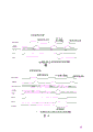
Fig. 5 is the explanation sequential chart that is used for the control signal of existing system shown in Figure 2;
Fig. 6 is the sequential chart of explanation control signal of most preferred embodiment according to the present invention.
Elaborate most preferred embodiment of the present invention now with reference to accompanying drawing.With reference to Fig. 1, one is used to implement optimizer system of the present invention and comprises a CPU100, for example it is Intel Company's 80386 microprocessor, and it is by comprising control bus 110, and a group system signal bus 105 of data bus 115 and address bus 120 is connected to other system element.The permanent primary memory 130 and the memory controller 135 of 125, one immediated addressing read/write store of ROM (read-only memory) (ROM) of resident system logic of keeping is connected to bus 105.
For according to system of the present invention, preferablely provided a point of contact 140, to allow bus interface equipment 140; For example bus master can be operatively connected to the data bus of system bus 105.As being familiar with in the prior art, normally use circuit board is inserted into this connection the (only representing with side figure) in the groove that is suitable for the card border connection in Fig. 1.These interfacing equipments 145 can be connected to other various equipment, for example I/O (I/O) equipment 150.Equipment as 150, for example it can comprise disc driver or tape unit (not shown).Can be the interfacing equipment 145 of bus master device and the system arrangement of control data bus 115 this comprising, it is the Micro Channel Architecture that is specifically designed to IBM Corporation, the latter has detailed description in IBM Corporation's handbook, its exercise question is " personal system/2 hardware interface technical Reference 68X2330 ".For this system, a center judges that controller 155 foundation are used for the right of priority of the equipment of control data bus 115, and is familiar with as people, and the data that-dma controller 160 is coordinated the reality on this bus transmit.One group of assignment of typically judging priority level of table 1 explanation.
Table 1
Judge once
Level is assigned
-2 memory refresses
-1 error correction
0 DMA port 0
1 DMA port one
2 DMA ports 2
3 DMA ports 3
4 DMA ports 4
5 DMA ports 5
6 DMA ports 6
7 DMA ports 7
8 is standby
9 is standby
A is standby
B is standby
C is standby
D is standby
E is standby
F system plugin processor
Referring now to Fig. 2, the prior art comprises path 200, it provides the connection between center judgement control 155 and the CPU, so that (not shown) is according to the signal input transmission terminating operation signal (" HOLD ") of concrete processor (as using CPU) on lead-in wire.And path 210 is to be used for transmitting an answer signal to be back to judgement control 155.As pointing out, the passage (referring to Fig. 1) that control is total 110 is used for distribute data bus 115.
Passage 200 transmits+and the ARB/-GRANT signal is when setting up judgement that bus occupies when taking place (ARB), and when occupying definite (GRANT), is used for recognition cycle, and different main frames 230 can be used for responsible assignment to occupying.Passage 240 is used for transmission-PREEPT signal, the one or more main process equipments of this signal indication, and for example equipment 240, comprise also that CPU100 is waiting for data bus 115 is carried out access.Passage 250 transmits a BURST signal, and this signal is being assert whether have the equipment of the ability of multiple transmission or character group transmission so that point out it by equipment 240 when it occupies data bus 115.
It can also be seen that from figure the judgement bus 260 that includes four lines (0-3) is connected to this center and judges control 155, assert and judges rank on these four lines, to get data bus 115 the right of possession corporeal right, then, during assert time GRANT on the passage 220, go the recognition holder.
With reference now to Fig. 3,, the logical circuit 300 of signalling channel 200 ' sensing complex 305, according to the present invention, this complex 305 inserts a delay, and the HOLD signal is produced an improvement of consequently representing with signal+CPUHOLD, this+the CPUHOLD signal is added to the terminating operation input port of CPU100.For 80386 of Intel Company, it can be " HOLD " of PGA pattern.One demoder 310 provides WRITE signal through 320 pairs of these logical circuits 300 of line, and it is used to that new delay width information is write register 400(and sees Fig. 4), this register is added to timer 410 through bus 420.
Then referring to Fig. 4, AND door 430 be used for receiving line 200 ' on+inversion signal of HOLD signal, on the line 220+inversion signal of ARB/-GRANT signal, and the information of the bus holder on the ARB bus 260.The output of this AND door 430 is+the CPUSEL signal that this signal is added to timer 410, is used for the cycle of appointment on bus 420 is triggered timeout signal on online 440.This signal+CPUSEL signal will stop request and send from judging control when one, and this CPU100 removes to trigger the timeout signal+DELAY on the line 450 when occupying DATA bus 115 under such certain situation.(GRANT is effective, and judges that rank is 1111, and the heuristicimal code F of expression is used for discerning CPU in the table 1).Line 200 ' on signal+HOLD and+inversion signal of DELAY is added to AND door 460 be added to CPU100(and see Fig. 3 so that on 1a line 470, produce) signal+CPUHOLD.Do one relatively as long as the sequential chart (Fig. 5) of prior art will be described with the sequential chart (Fig. 6) of explanation most preferred embodiment, the improvement benefit of this termination signal+HOLD will come into plain view.As noted above this CPU100 can keep occupying data bus 115 like that, till delay period stops.
The present invention has carried out detailed description with reference to most preferred embodiment, but, be appreciated that and enlighten wherein multiple modification those skilled in the art, but in order to determine scope of the present invention, must be with reference to claim, because claim is considered any equivalent of applicant's appellation.

Claims (1)

1, in a computer system, have a master processor, this master processor can enough termination signals be excited to disarmed state; One main data bus is arranged, it is distributed by decision logic, this decision logic when bus request arrives comprise said master processor more than a main process equipment time, select the bus holder repeatedly according to predetermined level of priority, this master processor is assigned absent level of priority, and a feature that preferentially occupies delay circuit is:
In case decision logic is selected said master processor, detect logic and produce a selection signal, and
One from the path that the termination input end of said decision logic equipment and said master processor extends, delay logic is connected to time delayed signal.
CN90109372A 1989-10-23 1990-10-23 Delay logic for preventing CPU lockout from bus ownership Expired - Fee Related CN1024962C (en)

Applications Claiming Priority (3)

Application Number Priority Date Filing Date Title
US42576589A 1989-10-23 1989-10-23
US425,765 1989-10-23
US07/425,765 1989-10-23

Publications (2)

Publication Number Publication Date
CN1051802A true CN1051802A (en) 1991-05-29
CN1024962C CN1024962C (en) 1994-06-08

Family

ID=23687939

Family Applications (1)

Application Number Title Priority Date Filing Date
CN90109372A Expired - Fee Related CN1024962C (en) 1989-10-23 1990-10-23 Delay logic for preventing CPU lockout from bus ownership

Country Status (7)

Country Link
EP (1) EP0425194B1 (en)
JP (1) JPH06105448B2 (en)
KR (1) KR930005726B1 (en)
CN (1) CN1024962C (en)
CA (1) CA2021826A1 (en)
DE (1) DE69024912T2 (en)
TW (1) TW369632B (en)

Cited By (2)

* Cited by examiner, † Cited by third party
Publication number Priority date Publication date Assignee Title
CN100388762C (en) * 2004-07-22 2008-05-14 奥林巴斯株式会社 bus request control circuit
CN103210382A (en) * 2010-10-20 2013-07-17 高通股份有限公司 Arbitrates bus transactions on a communication bus based on bus device health information and related power management

Families Citing this family (5)

* Cited by examiner, † Cited by third party
Publication number Priority date Publication date Assignee Title
CA2068010C (en) * 1991-08-30 1996-10-22 Robert Chih-Tsin Eng Alternate master bursting data rate management techniques for use in computer systems having dual bus architecture
GB9418753D0 (en) * 1994-09-16 1994-11-02 Ionica L3 Limited Process circuitry
CN1215636C (en) 2001-12-31 2005-08-17 艾默生网络能源有限公司 Method of establishing host machine in multi-module parallel system
FR2894696A1 (en) * 2005-12-14 2007-06-15 Thomson Licensing Sas METHOD FOR ACCESSING A DATA TRANSMISSION BUS, DEVICE AND CORRESPONDING SYSTEM
CN113094158B (en) * 2021-03-15 2024-07-02 国政通科技有限公司 Service drive calling method, calling device, electronic equipment and storage medium

Family Cites Families (4)

* Cited by examiner, † Cited by third party
Publication number Priority date Publication date Assignee Title
US4593350A (en) * 1983-05-25 1986-06-03 Rca Corporation Distributed processor with periodic data transfer from each memory to like addresses of all other memories
AU4907285A (en) * 1984-11-09 1986-05-15 Spacelabs, Inc. Communications bus broadcasting
JPS623364A (en) * 1985-06-28 1987-01-09 Fujitsu Ltd Bus occupation control system
US4980854A (en) * 1987-05-01 1990-12-25 Digital Equipment Corporation Lookahead bus arbitration system with override of conditional access grants by bus cycle extensions for multicycle data transfers

Cited By (4)

* Cited by examiner, † Cited by third party
Publication number Priority date Publication date Assignee Title
CN100388762C (en) * 2004-07-22 2008-05-14 奥林巴斯株式会社 bus request control circuit
CN103210382A (en) * 2010-10-20 2013-07-17 高通股份有限公司 Arbitrates bus transactions on a communication bus based on bus device health information and related power management
US9064050B2 (en) 2010-10-20 2015-06-23 Qualcomm Incorporated Arbitrating bus transactions on a communications bus based on bus device health information and related power management
CN103210382B (en) * 2010-10-20 2016-02-24 高通股份有限公司 Arbitrates bus transactions on a communication bus based on bus device health information and related power management

Also Published As

Publication number Publication date
CN1024962C (en) 1994-06-08
EP0425194A3 (en) 1991-10-23
DE69024912D1 (en) 1996-02-29
CA2021826A1 (en) 1991-04-24
KR910008592A (en) 1991-05-31
JPH03142650A (en) 1991-06-18
TW369632B (en) 1999-09-11
KR930005726B1 (en) 1993-06-24
EP0425194A2 (en) 1991-05-02
EP0425194B1 (en) 1996-01-17
JPH06105448B2 (en) 1994-12-21
DE69024912T2 (en) 1996-08-08

Similar Documents

Publication Publication Date Title
US5237567A (en) Processor communication bus
US5404538A (en) Method and apparatus for multilevel bus arbitration
US4320457A (en) Communication bus acquisition circuit
US4972313A (en) Bus access control for a multi-host system using successively decremented arbitration delay periods to allocate bus access among the hosts
US5257356A (en) Method of reducing wasted bus bandwidth due to slow responding slaves in a multiprocessor computer system
US5239651A (en) Method of and apparatus for arbitration based on the availability of resources
EP0428330A2 (en) Computer interface circuit
EP0588521A1 (en) System and method for regulating access to direct access storage devices in data processing systems
CN1013068B (en) Computer system with programmable direct memory access control
CA1164573A (en) Arbitration controller providing for access of a common resource by a plurality of central processing units
EP0675444B1 (en) Multiple arbitration scheme
EP0327203A2 (en) NxM arbitrating non-blocking high bandwidth switch
CN1214332C (en) System and method for implementing multi-level interrupt scheme in computer system
CN1051802A (en) Delay logic used to prevent CPU from being blocked due to bus occupation
WO2007067739A1 (en) Memory access request arbitration
US6430640B1 (en) Self-arbitrating, self-granting resource access
US5450591A (en) Channel selection arbitration
EP0425181B1 (en) Preference circuit for a computer system
EP0836143A3 (en) Method and apparatus for improving fairness in bus arbitration
US5241629A (en) Method and apparatus for a high performance round robin distributed bus priority network
KR950008228B1 (en) Computer system with direct memory access channd arbitration
JPS62283752A (en) Buffer allocating system in host computer
JPH04359353A (en) Bus controller
JPH0399355A (en) time sharing system
JPS61122769A (en) Bus control system

Legal Events

Date Code Title Description
C10 Entry into substantive examination
SE01 Entry into force of request for substantive examination
C06 Publication
PB01 Publication
C14 Grant of patent or utility model
GR01 Patent grant
C15 Extension of patent right duration from 15 to 20 years for appl. with date before 31.12.1992 and still valid on 11.12.2001 (patent law change 1993)
OR01 Other related matters
C19 Lapse of patent right due to non-payment of the annual fee
CF01 Termination of patent right due to non-payment of annual fee