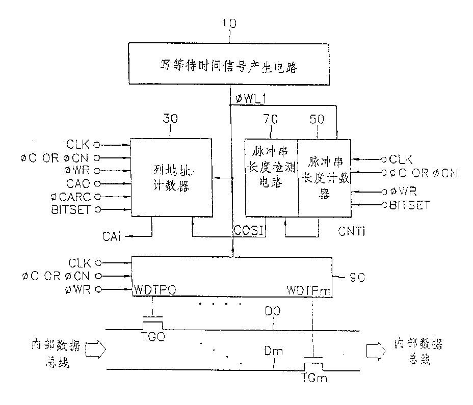
Most preferred embodiment of the present invention will be applied to the synchronous dynamic ram of mega bit order.Fig. 1 is illustrated in and comprises the ingredient of implementing a kind of write latency control function in the semiconductor storage arrangement.Write latency signal generating circuit 10 produces the write latency signal WL1 that determines the write latency value.This write latency signal WL1 can be provided with write latency value " 0 " or " 1 ", and its production process is shown among Fig. 2.Column address counter 30 receiving system clock CLK, CAS effective information signal C (or the CAS effective information amplifying signal CN when the write latency value is " n "), write permission (WE) effective information signal WR, column address signal CAO, column address reset signal CARC, position signalization BITSET and write latency signal WL1, and will be sent to column address buffer by many column address signals of column address signal CAO counting, burst length counter 50 receiving system clock CLK, CAS effective information signal C (or the CAS effective information amplifying signal CN when the write latency value is " n "), WE effective information signal WR, position signalization BITSET and write latency signal WL1, and burst length signal calculated CNTi (i is one of 0-8 here) is added to pulse train length detecting circuit 70.This pulse train length detecting circuit 70 will be compared with the burst length signal of stipulating by the burst length signal calculated CNTi that burst length counter 50 produces, to produce burst length read output signal COSi, and this burst length read output signal COSi is sent to column address counter 30, to control the calculating operation of this column address signal.Data transfer switch circuit 90 receiving system clock CLK, CAS effective information signal C (or the CAS effective information amplifying signal CN when the write latency value is " n "), WE effective information signal WR, write latency signal WL1, and generation data transfer switch signal WDTPO-WDTPm is used for control data transfer gate TGO-TGm.
System clock CLK is provided by microprocessor of chip exterior etc.
For example it has 100MHZ, the fixed frequency of 66MHZ or 33MHZ.This system clock CLK is used as the radix that the various running times are set in synchronous semiconductor memory device.CAS effective information signal C is produced by cas buffer device (not shown), and the column address gating signal CAS that is provided by chip exterior is provided this impact damper.Effectively column address gating signal CAS is effective to logic " low " for this CAS effective information signal response, and maintains logic " height " during one-period.CAS effective information amplifying signal CN relative set write latency value produces the number of CAS effective information signal C delayed time system clock CLK clock, and its production process will be described with reference to figure 3.WE effective information signal WR is produced by WE impact damper (not shown), the written allowance signal WE that is provided by chip exterior is provided for this impact damper, and response effectively this written allowance signal WE is effective to logic " low ".During write cycle time, only when initial column address signal was applied in and maintains logic " height ", WE effective information signal WR maintained logic " low ".Column address reset signal CARC is effective, with position signalization BITSET, and the CAS effective information signal C that response is produced by the cas buffer device, and during write cycle time, maintain logic " height ".Position signalization BITSET is only as response CAS effective information signal C, when the initial column address signal is provided to the effective pulse signal of logic " height ", with control column address counter 30 and burst length counter 50.Other details of these signals are understood easily according to following explanation.
The example of key diagram 1 write latency signal generating circuit among Fig. 2 A-2C.In Fig. 2 A, bonding wire 4 is used between the solder joint 6 in ground voltage lead-in wire 2 and the chips welding process.If bonding wire 4 is linked ground voltage lead-in wire 2, patrol " low " signal and be applied to reverser chain 14, and produce logic " height " write waiting signal WL1.In such example, the write latency value is " 1 ", this means according to the written allowance signal WE that provides, and after a clock of system clock, the input data are sent to internal data bus.If solder joint 6 is not linked ground voltage lead-in wire 2, the current potential of node 12 is placed in logic " height " by PMOS transistor 8 and produces the write latency signal WL1 of logic " low ".Afterwards, write latency is " 0 ", and this means that synchronous dynamic ram do not carry out write latency operation.
In Fig. 2 B, fuse 3 is used among the stand-by period process of the test.If fuse 3 is linked power Vcc, produce the write latency signal WL1 (in the case, the write latency value is " 0 ") of logic " height " by chain of inverters 14.If fuse 3 disconnects from power Vcc, produce the write latency signal WL1 (in the case, the write latency value is " 1 ") of logic " height ".In Fig. 2 C, use a kind of program format that produces write latency signal WL1 by WCBR clock WCBR logic state control and that respond any column address signal CAi here.If WCBR clock WCBR is set to logic " height ", the phase inverter of being made up of PMOS transistor 11 and nmos pass transistor 15 will move.The input of this phase inverter is column address signal CAi, and its output is added to latch 19.The output of this latch 19 is added to the Sheffer stroke gate (not shown) by reverser 21.If column address signal CAi is logic " low ", then produce the write latency signal WLi (in the case, the write latency value is " 0 ") of logic " low ".And if this column address signal CAi is logic " height ", then produce the write latency signal WLi (in the case, the write latency value is " 1 ") of logic " height ".
For the write latency value being set, as shown in Figure 3, need be used to produce the circuit of CAS effective information amplifying signal CN to " n " (being equal to or greater than " 2 ").For producing several CAS effective information signal CO- Cn-1, CAS effective information signal C is added to by latch L10, L
11..., L
12, L
13And transfer gate G
10, G
11... G
12, G
13G
14The shift register of forming.Transfer gate is the CMOS pattern.The N-type of adjacent transfer gate and P-type electrode are oppositely placed, and are controlled by system clock CLK.The several CAS effective information signal CO- Cn-1 that produce by this shift register are added to rejection gate NR10.The output of rejection gate NR10 is added to phase inverter 111, has the CAS effective information amplifying signal CN of relevant several CAS effective information signals with generation.If use this CAS effective information amplifying signal CN, the input data respond n system clock CLK after written allowance signal is effective, transfer to internal data bus.
The calculation stage of Fig. 4 A and 4B presentation graphs 1 column address counter 30.Column address signal CAi-1 and the carry signal CRi-1 that is produced by prime are provided to produce the calculated column address signal CAi of desire.Though do not show in the drawings, be used for the identical of 4A and 4B around the circuit structure of each calculation stage of common column address counter of synchronous semiconductor memory device, unless this column address signal and carry signal are provided by prime.The public circuit structure that is illustrated among Fig. 4 A and the 4B is the technology of knowing.And the column address counter of Fig. 4 A explanation when the write latency value is " 0 ", in Fig. 4 B, write latency information is considered to be used for producing this column address signal.With reference to Fig. 4 B, receive CAS effective information signal C (the perhaps CAS effective information amplifying signal CN when the write latency value is put " n "), the output and the column address reset signal CARC of the Sheffer stroke gate 46 of WE effective information signal WR and write latency signal WL1 are added to Sheffer stroke gate 47 together.The output of Sheffer stroke gate 47 is added to Sheffer stroke gate 31 by a phase inverter 48.Therefore, the column address reset signal CARC ' that produces by phase inverter 48 has write latency information.Should be pointed out that Fig. 4 B has considered to use the write latency information of column address calculating operation by the present invention.
The burst length counter 50 of Fig. 5 A and 5B presentation graphs 1 also produces burst length signal calculated CNTi (i is a number one of among the 0-8) here.Burst length counter when Fig. 5 A explanation is not considered to write outstanding message or write latency value and is " 0 ", and the burst length counter of Fig. 5 B explanation when consideration write latency information.In Fig. 5 A, the rejection gate 51 that receives position signalization BITSET and reset signal S produces the COSSET signal by phase inverter 52, is used for gating pulse string length calculating operation.This burst length calculation control signal COSSET is added to rejection gate 54.This rejection gate 54 is by system clock CLK control and receive the carry signal CRi-1 that is produced by prime.The output control CMOS transfer gate 56 and 58 of rejection gate 54.Latch 57 is connected between transfer gate 56 outputs and transfer gate 58 inputs.The output of phase inverter 52 is connected to the grid of nmos pass transistor 53, and this nmos pass transistor 53 is connected between latch 57 input ends and the substrate voltage Vss.Latch 59 and phase inverter 60 are serially connected between the input end of the output terminal of transfer gate 58 and transfer gate 56.Burst length signal calculated CNTi produces from latch 59.
In Fig. 5 B, write latency signal WL1 is added to the Sheffer stroke gate 61 by CAS effective information signal C (or the CAS effective information amplifying signal CN when the write latency value is put " n ") and WE effective information signal WR control.The output of Sheffer stroke gate 61 is added to the Sheffer stroke gate 62 by reset signal S control.And the output of Sheffer stroke gate 62 is added to the rejection gate 51 by position signalization BITSET control.Therefore, the burst length calculation control signal COSSET ' that produces by phase inverter 52 has write latency information.Other be used to produce the identical of the circuit structure of burst length signal calculated CNTi and Fig. 5 A.
Fig. 6 indicating impulse string testing circuit 70.This pulse length testing circuit receives the burst length signal calculated CNTO-CNT8 that is produced by the burst length counter with each calculation stage that is shown among Fig. 5 A or the 5B, and produces train of impulses detection signal COSI, is used for determining whether this train of impulses finishes.Burst length detection signal COSI is with the burst length signal SZ 2 of burst length signal calculated CNTO-CNT8 with the regulation that the generation of circuit (not shown) is set by operator scheme, SZ 4, SZ 8, SZ 16, SZ 32, SZ 64, and SZ 128, and SZ 256 and SZ 512 compare and obtain.The circuit of Fig. 6 is open in Korean Patent 93-7127, and this patent transfers same assignee of the present invention.Should be pointed out that in the detection burst length and consider write latency information in the time.
The data transfer switch circuit 90 that is shown in the Fig. 1 among Fig. 7 A and the 7B produces one of control chart 1 data transfer gate TGo-TGm data transfer switch signal WDTPi (i is one of o-m) here.Data transfer switch circuit when write latency information is not considered in Fig. 7 A explanation, and Fig. 7 B illustrates the data transfer switch circuit when considering write latency information.In Fig. 7 A, system clock CLK is added to Sheffer stroke gate 94 by the chain of inverters of being made up of four phase inverters 91.Receive WE effective information signal WR and reset signal S Sheffer stroke gate 92 output by-phase inverter 93 also is added to this Sheffer stroke gate 94, and column address signal CAi also is added to Sheffer stroke gate 94.This Sheffer stroke gate 94 produces this data transfer switch signal WDTPi by a chain of inverters of being made up of three phase inverters.Though the relative column address signal of the data transfer switch circuit of Fig. 7 A produces a data switch transfer signal, the quantity of column address signal is should be respectively identical with the quantity of the quantity of Sheffer stroke gate 94 and chain of inverters 95.The structure of Fig. 7 B is identical with Fig. 7 A, and the output that different is receives the Sheffer stroke gate 96 of CAS effective information signal C (or the CAS effective information amplifying signal CN when the write latency value is " n ") and write latency signal WL1 also is added to the Sheffer stroke gate 92 by WE effective information signal WR and repositioning information S.
The write latency control operation of the present invention that constitutes in a manner described will be described now.As shown in Figure 1, the write latency signal WL1 that is produced by write latency signal generating circuit 10 should be added to column address counter 30 simultaneously, pulse length counter 50 and data transfer switch circuit 90, so that by means of column address gating signal CAS and written allowance signal WE, begin to be sent to internal data bus execution time control entirely from data input buffer up to write data after by the data transfer gate from write cycle time.Arrive this, as from Fig. 4 B, what 5B and 7B understood, the signal with write latency information keeps the logic open operation at column address counter 30, burst length counter 50 and data transfer switch circuit 90 places.
Suppose the write latency value for " n ", write latency signal WL1 and the CAS effective information amplifying signal CN that locates logic " height " are added to the Sheffer stroke gate 46 of Fig. 4 B column address counter.During writing with the phase, because WE effective information signal WR place's logic " height ", so Sheffer stroke gate 46 is output as logic " low ".Be under the logic " high " state at write latency signal WL1, (this time is called as " retention time " when CAS effective information amplifying signal CN maintains logic " height ", and use " TH " expression in the drawings), maintain logic " low " by the output of the rejection gate 32 of system clock CLK control.Because during this retention time, transfer gate 40 disconnects, and transfer gate 43 is connected, then during this retention time, column address signal CAi maintains current logic state.
Similarly, if the write latency value is " n ", because the output in the Sheffer stroke gate 61 of this retention time Fig. 5 B burst length counter is logic " low ", so during this retention time, maintain logic " low " by the output of the rejection gate 54 of system clock CLK control.Transfer gate 56 disconnects, and transfer gate 68 is connected, and therefore will keep the present logic state in burst length signal calculated CNTi place during this retention time.In the data transfer switch circuit of Fig. 7 B, if the write latency value is " n ", owing to during this retention time, receive the output place logic " low " of the Sheffer stroke gate 96 of write latency signal WL1 and CAS effective information amplifying signal CN, then during this retention time, the output that receives the Sheffer stroke gate 94 of column address signal CAi maintains logic " height ".Because during this retention time, data transfer switch signal WDTPi maintains logic " low ", so the corresponding data transfer gate shown in Fig. 1 is disconnected.
Therefore, during this retention time, because the current logic state, the output that this column address counter, burst length counter and data transfer switch circuit produce is constant.This retention time is determined by CAS effective information signal and the write latency signal with write latency information.
Fig. 8 A-8C explanation is only when the sequential chart of Fig. 1 data transfer switch circuit 90 during without the write latency information Control.In Fig. 8 A, the write latency value is " 0 ", and input data D
1And D
2Generally response data transfer switch signal WDTP1 and WDTP2 carry out access respectively.Simultaneously, shown in Fig. 8 B and 8C, when the write latency value is respectively " 1 " and " 2 ", because during 2 times of retention time 2TH of the retention time of Fig. 8 B TH and Fig. 8 C, this column address signal CAi is not considered and maintains current state, so produce an invalid data transfer switch signal WDTP1 (by " IV " expression) (at the time of Fig. 8 B t at each system clock CLK
1T with Fig. 8 c
2).Therefore, invalid input data D1 transfers to internal data bus by data transfer gate TG1 and will produce fault.
Fig. 9 explanation can't help to write outstanding message control at the data transfer switch circuit 90 that has only Fig. 1, and this write latency value is under the situation of " 1 ", the sequential chart when the I/O masking operation is carried out by an output/output shielded signal DQM.As shown in the figure, invalid input data D
1By at time t
1Ineffectually the data transfer switch signal WDTP1 of Chan Shenging is sent to internal data bus.Like this, at time t
2Valid data transfer switch signal WDTP1 (with dot-and-dash line " a " expression) and can't help to produce at the I/O shielded signal DQM that time tM starts.Therefore, be transferred to writing of inner input bus and import data D
1Do not shift at dot-and-dash line " b ".Thus, as shown in figure 10, if data transfer switch circuit by the write latency information Control, data transfer switch signal WDTP1 is not at the time t shown in dot-and-dash line among the figure " C "
1Produce, but at t
2Produce.Therefore should import data D1 usually transfers to internal data bus.
So far the operation described is expressed as acquisition and should carries out processing how by effect of the present invention.
Figure 11 A and the best enforcement of 11B explanation sequential chart of the present invention.When the write latency value was " 0 " (promptly when write latency signal WL1 is logic " low "), the sequential chart of Figure 11 A was represented the A by Fig. 4,5A, and 6 operations of carrying out with 7A are identical with Fig. 8 A.
Shown in Figure 11 B, when the write latency value is " 1 " (promptly when write latency signal WL1 is logic " height "), be applicable to Fig. 2,4B, 5B, 6 and 7B.If position signalization BITSET is started by the CAS effective information signal C that starts to logic " height ", the column address CAi-1 that calculates in prime is not stored in the latch 42 by the transfer gate among Fig. 4 B 38, afterwards, system clock CLK rises to logic " height ", and transfer gate 43 is connected, and produces column address signal CAi (CAO) thus.Because write latency signal WL1 is a logic " height " (and CAS effective information signal C and WE effective information signal WR are logic " height "), so the output of the NOR door 32 of control transfer gate 40 and 43 maintains logic " low " therefore, before retention time TH, column address signal CAi (CAo) maintains the current logic state, and during retention time TH, the output of NOR door 32 maintains logic " low ".Equally, in Fig. 5 B, because burst length calculation control signal COSSET ' maintains logic " height " during retention time TH, so burst length signal calculated CNTi maintains the current logic state.Equally, in Fig. 7 B, because the output of Sheffer stroke gate 94 maintains logic " low " by write latency signal WL1 and the CAS effective information signal C that is in logic " height " during retention time TH, so data transfer switch signal WDTPO is postponed by this retention time TH.
After this retention time TH, because CAS effective information signal C drops to logic " low ", so column address reset signal CARC and burst length calculation control signal COSSET ' are set to logic " height " and " low " respectively.Therefore, in Fig. 4 B, the formation of column address signal CAi (CAO) be by trigger up and down by means of system clock LCK continuous finish equally in Fig. 5 B, finish the formation of burst length signal calculated CNTi (CNTO).In Fig. 7 B, because the output of phase inverter 93 is logic " height ", the column address signal CAi (CAO) of Sheffer stroke gate 94 response logic " height " and the following triggering for generating logic " low " of system clock CLK.Produced the data transfer switch signal WDTPO of logic " height " like this, and corresponding transfer gate TGO connects, therefore shift and write input data D
1To internal data bus.Next input data D
1Transfer process carried out similarly.
Write latency position if " n ", the CAS effective information amplifying signal CN that then uses Fig. 3 circuit to produce, and the retention time becomes and is n * TH.
When specific embodiment of the present invention was disclosed right at this already, will make some remodeling easily to those skilled in the art.For example, the circuit of Fig. 3 can use other row coherent signal or write coherent signal, rather than goes to produce write latency value " n " with CAS effective information signal C.
As mentioned above, obtain to be used to control the circuit of write latency value easily.Therefore, the stability of the operation of synchronous semiconductor memory device and unfailing performance improve.