CN1054018C - Adaptive video peaking circuitry using cross-faders - Google Patents
Adaptive video peaking circuitry using cross-faders Download PDFInfo
- Publication number
- CN1054018C CN1054018C CN93119799A CN93119799A CN1054018C CN 1054018 C CN1054018 C CN 1054018C CN 93119799 A CN93119799 A CN 93119799A CN 93119799 A CN93119799 A CN 93119799A CN 1054018 C CN1054018 C CN 1054018C
- Authority
- CN
- China
- Prior art keywords
- signal
- edge detector
- response
- comb filter
- horizontal
- Prior art date
- Legal status (The legal status is an assumption and is not a legal conclusion. Google has not performed a legal analysis and makes no representation as to the accuracy of the status listed.)
- Expired - Fee Related
Links
Images



Classifications
-
- H—ELECTRICITY
- H04—ELECTRIC COMMUNICATION TECHNIQUE
- H04N—PICTORIAL COMMUNICATION, e.g. TELEVISION
- H04N9/00—Details of colour television systems
- H04N9/77—Circuits for processing the brightness signal and the chrominance signal relative to each other, e.g. adjusting the phase of the brightness signal relative to the colour signal, correcting differential gain or differential phase
- H04N9/78—Circuits for processing the brightness signal and the chrominance signal relative to each other, e.g. adjusting the phase of the brightness signal relative to the colour signal, correcting differential gain or differential phase for separating the brightness signal or the chrominance signal from the colour television signal, e.g. using comb filter
-
- H—ELECTRICITY
- H04—ELECTRIC COMMUNICATION TECHNIQUE
- H04N—PICTORIAL COMMUNICATION, e.g. TELEVISION
- H04N11/00—Colour television systems
- H04N11/06—Transmission systems characterised by the manner in which the individual colour picture signal components are combined
- H04N11/12—Transmission systems characterised by the manner in which the individual colour picture signal components are combined using simultaneous signals only
- H04N11/14—Transmission systems characterised by the manner in which the individual colour picture signal components are combined using simultaneous signals only in which one signal, modulated in phase and amplitude, conveys colour information and a second signal conveys brightness information, e.g. NTSC-system
-
- H—ELECTRICITY
- H04—ELECTRIC COMMUNICATION TECHNIQUE
- H04N—PICTORIAL COMMUNICATION, e.g. TELEVISION
- H04N5/00—Details of television systems
- H04N5/14—Picture signal circuitry for video frequency region
- H04N5/20—Circuitry for controlling amplitude response
Landscapes
- Engineering & Computer Science (AREA)
- Multimedia (AREA)
- Signal Processing (AREA)
- Processing Of Color Television Signals (AREA)
Abstract
通过组合各种被延时的视频信号的响应,将所说的视频信号的水平和垂直蜂化信号分离。按照由一个平滑转换器控制信号所确定的比率,该平滑转换器将已分离的水平和垂直峰化信号组合。一相关器响应对于该视频信号的各种延时响应中的某些来产生表示在该视频信号中的垂直和水平相关程度的一个输出信号。该相关器的输出信号编址在一个提供该平滑转换器控制信号的一个只读存储器。
The horizontal and vertical buzzing of the video signal is separated by combining the responses of the various delayed video signals. The crossover combines the separated horizontal and vertical peaking signals according to a ratio determined by a crossover control signal. A correlator is responsive to some of the various delayed responses to the video signal to produce an output signal indicative of the degree of vertical and horizontal correlation in the video signal. The output signal of the correlator is addressed to a read only memory which provides the control signal of the cross-slipper.
Description
本发明涉及自适应视频峰化电路,可与一亮/色分离器结合使用,以便从一个NTSC复合视频信号分离出亮度信号(即“亮”或“Y”)和色度信号(即“色”或“C”)。The present invention relates to adaptive video peaking circuits that can be used in conjunction with a Bright/Color Separator to separate the Luminance (i.e. "Light" or "Y") and Chroma (i.e. "Chroma") signals from an NTSC composite video signal. " or "C").
1979年12月11日授予R.C.Beutel的题为“具有改进亮度响应的梳状滤波器”的4178609号美国专利描述了一个响应复合电视信号用以将亮度和色度彼此各自地分开的自适应行间梳状滤波器。与梳状滤波器一起使用的一个检波器检测在色度连续行中的相关缺欠,响应这一检测来改变梳状滤波器的操作,以便降低在已分离的亮度信号中的未被消除的色信号。U.S. Patent No. 4,178,609, issued December 11, 1979 to R.C. Beutel, entitled "Comb Filter with Improved Luminance Response," describes an adaptive line that responds to a composite television signal to separate luminance and chrominance from each other. comb filter. A detector used with the comb filter detects correlation defects in the chrominance succession lines and in response to this detection alters the operation of the comb filter so as to reduce unremoved chrominance in the separated luminance signal. Signal.
1985年2月5日授于O.H.Pritchard的题为“用于逐帧梳状滤波复合电视信号的装置”的4498099号美国专利描述了对在移动边缘部分劣质双影的降低。在当移动边缘被检测期间,由帧梳状滤波所分离的色信号被低通滤波并与由帧梳状滤波所分离的亮度信号组合,从而提供一个更好的被分离的亮度信号,以取代简单由帧梳状滤波所获的已分离的亮度信号。U.S. Patent No. 4,498,099, issued February 5, 1985 to O.H. Pritchard, entitled "Apparatus for Frame-by-Frame Comb Filtering of Composite Television Signals," describes the reduction of poor quality double images at moving edge portions. During periods when moving edges are detected, the color signal separated by frame comb filtering is low-pass filtered and combined with the luma signal separated by frame comb filtering to provide a better separated luma signal instead of The separated luminance signal obtained simply by frame comb filtering.
1985年2月5日授予R.M Bunting和A.A.Acampora的题为“用于逐帧梳状滤波复合电视信号的装置”的4498100号美国专利描述了对围绕再生彩色图象边周的色度失真的降低。当运动的边缘被检测期间,由帧梳状滤波所分离的色度信号被加到由帧梳状滤波所分离的亮度信号上,并将生成的结果做带通滤波,以提供一更好的已分离的色度信号,以便取代简单由帧梳状滤波所获得的已分离的色度信号。U.S. Patent No. 4,498,100, issued February 5, 1985 to R.M Bunting and A.A. Acampora, entitled "Apparatus for Comb Filtering a Composite Television Signal Frame by Frame," describes the reduction of chroma distortion around the perimeter of a reproduced color image . When moving edges are detected, the chrominance signal separated by frame comb filtering is added to the luma signal separated by frame comb filtering, and the resulting result is bandpass filtered to provide a better Separated chrominance signals to replace the separated chrominance signals obtained simply by frame comb filtering.
1989年4月4日授予Song Dongil和Kim Byung-Jin的题为“在电视接收机中的采用水平及垂直校正的自适应型亮/色信号分离电路”的4819062号美国专利描述了避免了对逐帧梳状滤波的需求的自适应梳状滤波。该4819062号美国专利的说明及附图被引用在此作为参考。U.S. Patent No. 4,819,062 to Song Dongil and Kim Byung-Jin on April 4, 1989, entitled "Adaptive Brightness/Colour Signal Separation Circuit Using Horizontal and Vertical Correction in Television Receiver" describes the avoidance of Adaptive comb filtering on demand for frame-by-frame comb filtering. The specification and drawings of US Patent No. 4,819,062 are incorporated herein by reference.
4819062号美国专利描述了低通和带通垂直滤波器的使用,以使当水平扫描通过图象场期间,在当信号用来表明边缘将出现时,该滤波器用以从NTSC复合视频信号分离亮度和色度信号。决定以哪种方法被选来从NTSC复合视频信号分离出亮度和色度信号是对应着在水平扫描边缘检波器的响应和垂直扫描边缘检波器的响应之间的比较结果。该水平扫描边缘检波器确定了该复合视频信号在水平方向上的相关性,而该垂直扫描边缘检波器确定了该复合视频信号在垂直方向上的相关性。U.S. Patent No. 4,819,062 describes the use of low-pass and band-pass vertical filters to separate luminance from an NTSC composite video signal when the signal is used to indicate that edges are to be present during horizontal scanning through the image field. and color signals. Determining which method has been selected to separate the luminance and chrominance signals from the NTSC composite video signal corresponds to a comparison between the response of the horizontal scan edge detector and the response of the vertical scan edge detector. The horizontal scan edge detector determines the correlation of the composite video signal in the horizontal direction, and the vertical scan edge detector determines the correlation of the composite video signal in the vertical direction.
4819062号美国专利还进一步描述了两种类型的用于边缘的峰化滤波器的选择性使用。当利用低通和带通垂直梳状滤波器从NTSC复合视频信号分离出亮度和色度信号时,水平高频成分则由一带通水平梳状滤波器从该低通垂直梳状滤波器的响应中被分离。当利用低通和带通水平梳状滤波器从NTSC复合视频信号分离出亮度和色度信号时,垂直高频成分则由一低通水平梳状滤波器从该带通垂直梳状滤波器的响应中被分离。US Patent No. 4819062 further describes the selective use of two types of peaking filters for edges. When the luminance and chrominance signals are separated from an NTSC composite video signal using a low-pass and band-pass vertical comb filter, the horizontal high-frequency components are determined by a band-pass horizontal comb filter from the response of the low-pass vertical comb filter. was separated. When the luminance and chrominance signals are separated from the NTSC composite video signal using low-pass and band-pass horizontal comb filters, the vertical high-frequency components are separated from the band-pass vertical comb filter by a low-pass horizontal comb filter. The response is separated.
由C.H.Strolle Jung-Wan KO和R.A.Schnitzler于1990年8月6日提交的题为“从一非折叠视频信号中除去折叠载波和边带”的、转让给三星电子公司的07/562,907号美国专利申请描述了软开关即平滑转换的使用,用于将低通垂直梳状滤波的亮度信号与低通水平梳状滤波的亮度信号相混合,这一混合是相对于在一个水平扫描边缘检波器对提供来进行自适应滤波的亮度信号的响应和一个垂直扫描边缘检波器对提供来进行自适应滤波的亮度信号的响应之间所作的比较而进行的。提供来进行低通垂直梳状滤波和低通水平梳状滤波的亮度信号被描述为是通过展开一个已折叠的频谱亮度信号所获得的,该折叠频谱亮度信号是从来自一VHS视频磁带记录接收的一个重放调频亮度载波解调的。U.S. Patent No. 07/562,907, assigned to Samsung Electronics Corporation, entitled "Removal of Folded Carrier and Sidebands from an Unfolded Video Signal," filed Aug. 6, 1990 by C.H. Strolle Jung-Wan KO and R.A. Schnitzler The application describes the use of soft switching, or smooth transitions, to mix a low-pass vertical comb-filtered luminance signal with a low-pass horizontal comb-filtered luminance signal relative to a pair of horizontally scanned edge detectors. A comparison is made between the response of a luminance signal supplied to the adaptive filtering and the response of a vertical scanning edge detector to the luminance signal supplied to the adaptive filtering. The luminance signal provided for low-pass vertical comb filtering and low-pass horizontal comb filtering is described as being obtained by unfolding a spectrally folded luminance signal received from a VHS video tape recording A playback of FM luminance carrier demodulated.
根据在07/562907号美国专利申请中使用和在此引用的专门术语,水平扫描遇到在白与黑之间的一个边缘被说成是遇到了一个“水平边缘”。该边缘可以是一个垂直线,但它被称为一个水平边缘是因为它是在一个水平扫描期间被遇到。相类似的,在一垂直扫描期间遇到的边缘叫作“垂直边缘”。“边缘”一词在技术上有时涉及“不连续性、”“过渡”、或“细节”。一个水平扫描边缘检波器是一个用以检测任何“水平边缘”的有效边缘检波器;而一个垂直扫描边缘检波器是一个用以检测任何“垂直边缘”的有效边缘检波器。Horizontal scanning encountering an edge between white and black is said to encounter a "horizontal edge," according to the terminology used in US Patent Application No. 07/562,907 and referenced herein. The edge can be a vertical line, but it is called a horizontal edge because it is encountered during a horizontal scan. Similarly, edges encountered during a vertical scan are called "vertical edges". The term "edge" technically sometimes refers to "discontinuity," "transition," or "detail." A horizontal scan edge detector is an effective edge detector that detects any "horizontal edge"; and a vertical scan edge detector is an effective edge detector that detects any "vertical edge".
依照本发明,4819062号美国专利所描述类型的自适应亮/色分离器被改进,以便使用于平滑转换而不是选择技术——即软转换而不是硬转换——出现在形成分离的亮度信号和分离的色度信号的过程中。这种改进降低了对构成的表面峰化过程中的自适应转变的可见性。In accordance with the present invention, an adaptive bright/color splitter of the type described in U.S. Patent No. 4,819,062 is modified so that smooth transitions rather than selection techniques—i.e., soft transitions rather than hard transitions—occur in forming separate luma signals and process of separating the chrominance signals. This improvement reduces the visibility of adaptive transitions during peaking of the constituent surfaces.
4819062号美国专利的附图1-7被包括在此作为参考,其被以下图1-6所扩大,简要地描述如下。Figures 1-7 of US Patent No. 4,819,062 are incorporated herein by reference, which are expanded by Figures 1-6 below, briefly described below.
图1是采用在本发明中的亮/色分离器的方框图;Fig. 1 is the block diagram that adopts bright/color separator in the present invention;
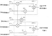
图2是可用于图1亮/色分离器中的平滑转换器电路以及对其控制的电路的详图;Fig. 2 is a detailed diagram of the smoother circuit and the circuit controlling it that can be used in the bright/color separator of Fig. 1;
图3是美国专利4819062的图1中用于平滑转换器电路的控制电路中由存储在只读存储器中的查阅表描述的转移函数曲线;Fig. 3 is the transfer function curve described by the look-up table stored in the read-only memory in the control circuit for the smoothing converter circuit in Fig. 1 of U.S. Patent 4819062;
图4是本发明另一实施例的电路框图,它以一个一半容量的只读存储器和一些数字算术电路取代了美国专利4819062的图1中用于平滑转换器电路的控制电路中的只读存储器;Fig. 4 is a circuit block diagram of another embodiment of the present invention, which replaces the ROM used in the control circuit of the smoothing converter circuit in Fig. 1 of U.S. Patent 4,819,062 with a ROM of half capacity and some digital arithmetic circuits ;
图5是由在图4所示的只读存储器中存储的查阅表所描述的一个转移函数曲线;Fig. 5 is a transfer function curve described by the look-up table stored in the read-only memory shown in Fig. 4;
图6和图7是方框图,每一个都表示可在本发明进一步的实施例中被用来改进或进一步改进的图1的亮/色分离器;Figure 6 and Figure 7 are block diagrams, each representing the bright/color separator of Figure 1 that can be used to improve or further improve in further embodiments of the present invention;
图8是一个可被用以改进图1亮/色分离器的方框图,以提供本发明一个可选用的实施例;Figure 8 is a block diagram that can be used to improve the bright/color separator of Figure 1 to provide an alternative embodiment of the present invention;
图9是可被用以对图1的亮/色分离器作又一改进的方框图,其中一平滑转换器电路的改进被包括在自适应色度滤波中;Fig. 9 is a block diagram that can be used to make yet another modification to the lightness/color separator of Fig. 1, wherein a smoother circuit modification is included in the adaptive chrominance filtering;
图10是由存储在图9中只读存储器中的查阅表所描述的一个转移函数曲线。FIG. 10 is a transfer function curve described by the look-up table stored in the read-only memory of FIG. 9. FIG.
图1中示出的亮/色分离器在许多方面与美国专利4819062的图4中示出的分离器相似,但区别在于,美国专利4819062的图4的数据选择装置60中的多路转换器MUX2和MUX3分别被平滑转换器XFD1和XFD2取代。而且,美国专利4819062的图4中的选择器装置在图1中由控制电路130取代。The bright/color splitter shown in FIG. 1 is similar in many respects to the splitter shown in FIG. 4 of US Patent 4,819,062, but the difference is that the multiplexer in the
控制电路130在结构上与美国专利4189062中的选择器装置30是类似的,但有以下的例外。所述专利中的数值比较器36由减法器136取代,并包括一个由来自减法器136的差的输出信号全部所编址的只读存储器137。ROM137产生加到平滑转换器(即软开关)XFD1和XFD2的控制信号。减法器136差输出信号的符号位被提取出来以加到多路转换器MUX1,以取代数值比较器36的输出信号,使得多路转换器MUX1的操作保持不变。第一绝对值操作装置34起到一个垂直扫描边缘检波器的作用,而在控制电路130中的第二绝对值操作装置35起到一个水平扫描边缘检波器的作用。The
复合电视信号延时装置10从连接点与二维空间滤波器20连接,滤波器的数字信号V1、V2、V3、V4、V5、V6、V7、V8、V9代表九个相邻图象单元或“象素”a、b、c、d、e、f、g、h、i的扫描方阵。这些方阵的现行的一个可出现在电视图象中作为一左侧顶行、中间和左侧象素a、b和c;左测一个中间行、中间和右侧象素d、e和f;以及左侧一个底行、中间和左侧象素g、h和i。用以产生第一分离色度响应C1的装置25包括在该二维空间滤波器20中,装置25在一带通垂直梳状滤波过程中以(-1)∶2∶(-1)的比率组合表示象素b、d与h的各种已延时的复合视频信号V2、V5和V8。用于产生第二分离色度响应的装置26被包括在二维空间滤波器20中,装置26在一带通水平梳状滤波过程中以(-1)∶2∶(-1)的比率组合表示象素c、d与e的各种已延时的复合视频信号V4、V5和V6。用于产生第一分离亮度响应Y1的装置27被包括在该二维空间滤波器20中,该装置27在一个低通垂直梳状滤波过程中组合表示象素b、d与h的各种已延时复合视频信号V2、V5与V8。用于产生第二分离亮度响应的装置28包括在该二维空间滤波器20中,该装置在一低通水平梳状滤波过程中以1∶2∶1的比率组合代表象素c、d与e的各种已延时的复合电视信号V4、V5和V6。Composite television
图2示出了在控制电路130中的其连接至ROM137的平滑转换器XFD1和XFD2的示意结构的具体情况。该平滑转换控制信号字从ROM137经总线32接收,在一数字减法器66中从整数一减去,或加1,以形成该平滑转换控制信号字的1的补码,而不是既以非互补又以互补的形式将平滑转换控制信号字存储在每一可编址位置。这就减半了所要求的ROM容量。该平滑转换器XFD1包括:一个第一数字乘法器63,借助于在总线32上接收的来自ROM137的平滑转换控制信号,该乘法器对经总线23接收的滤波器响应进行倍乘;第二数字乘法器64,借助于从减法器66提供的平滑转换控制信号的“1”的补码,该乘法器对经总线24接收的滤波器响应进行倍乘;一个第一数字加法器65,将乘法器63和64产生的信号加在一起,从该加法器65产生的和信号送到在亮度信号输出装置70中的延时单元90。平滑转换器XFD2包括:第三数字乘法器67,借助于在总线32上收到的来自ROM137的平滑转换控制信号,该乘法器67对在总线41上接收的滤波器40的响应进行倍乘,第四数字乘法器68,借助于从减法器66收到的平滑转换控制信号的“1”的补码,该乘法器68对经总线51接收的滤波器50的响应进行倍乘;一个第二数字加法器69,用于将从乘法器67和68输出的结果信号加在一起。加法器69产生的和信号送到在亮度信号输出装置中的非线性电路75,该非线性电路75核化(core)来自亮度高频峰化信号的噪声。FIG. 2 shows details of the schematic structure of smooth converters XFD1 and XFD2 connected to
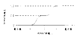
图3示出ROM137的输入/输出特性,它存储了一个用于平滑转换控制信号的查阅表。从减法器136送到ROM137的一个地址具有处在一个最小值,即负值和一个最大值即正值之间的值,产生一个具有在0和1之间的一个查阅表输出信号。该转换可根据平滑过渡曲线100进行,其中平滑转换器控制信号所具有的值是ROM137零值地址的一半。然而其它可替代形式的曲线,诸如曲线101或曲线102可被选用,在实验上可达到实现产生最佳的水平和垂直载波消除的特性。Fig. 3 shows the input/output characteristics of
图4中示出的电路在一定的条件下可以取代ROM137,它采用了具有等于ROM137的编址字存储器存储单元的的ROM1370。在作为来自减法器136的差信号的函数的平滑转换器控制信号的转移特性是关于该信号的值的一半为对称的场合,这种替代是可能的。来自减法器136的差信号被分解成包含有除符号位以外的全部比特的第一部分和一个包含符号位的第二部分,第一部分的比特被送到一个第一选择比特反相器1371,以选择比特补码;来自减法器136的差信号的符号位控制着由选择比特反相器1371选择的比特补码,并在一数字加法器1372中作为一个进位加到来自选择比特反相器1371的输出信号上。单元1371和1372组合起来起到一个绝对值电路的作用,即数字整流器的作用,以便将差信号的绝对值从减法器136加到ROM1370而作为寻址输入信号。The circuit shown in FIG. 4 can, under certain conditions, replace
图5示出存储在ROM1370中的查阅表。以ROM1370中读出的信号送到第二个选择比特反相器1373,以选择比特补码。来自减法器136的差信号的符号位控制着由选择比特反相器1373选择的比特补码,并作为来自选择比特反相器1373的输出信号的附带进位而被送到在一数字加法器1374中的值的一半上。来自数字加法器1374的和输出信号提供平滑转换器控制信号,该信号展现的转移特性是关于值的一半对称的、来自减法器136的差信号的函数,并对应于图3的曲线100的实例。FIG. 5 shows a look-up table stored in ROM1370. The signal read from ROM1370 is sent to the second
所要求保护的“只读存储器”在构思上要足够大,足以包含等效电路,该等效电路采用了与平滑转换器控制信号相关的信号的被降低的存储量,例如参考图3和5所描述的等效电路。The claimed "read only memory" is conceived to be large enough to contain an equivalent circuit employing a reduced amount of storage of signals related to the smoother control signal, see for example Figs. 3 and 5 The described equivalent circuit.
图5中的转移特性曲线可用一个X2n函数近似,并且,可通过用从取自减法器136的差信号开始重复地乘方的方式来算术地产生平滑转换器控制信号,而不是依靠对ROM表的查阅。用这种或任何其它的算术方法产生平滑转换器控制信号都是趋于缓慢的,因而在送往平滑转换器XFD1和XFD2的全部信号中都必须引入补偿延时。因而在本发明的优选实施例中采用的方法是利用来自ROM的表的查阅。The transfer characteristic curve in FIG. 5 can be approximated by an X2n function, and the cross-slipper control signal can be generated arithmetically by repeatedly squaring the difference signal from the
07/562,907号美国专利申请描述并要求保护了不带有第一绝对值操作装置34的水平扫描边缘检波器。该申请还描述及要求保护了不带有第一绝对值操作装置35的垂直扫描边缘检波器。这些边缘检波器是由本发明人以及他的合作者所研制,以便在录像带记录期间实现对亮度频谱折叠的残余不敏感,以及当进行梳状滤波以抑制这些出自亮度信号的残余时实现更加有特色的抗对角边缘的过渡,虽然在录像带记录期间对于亮度频谱折叠残余的抑制并不特别关注,但如本说明书中所描述的,在自适应视频峰化电路中,这些边缘检波器使其性能方面有改进并在亮/色分离方面有改进。这些边缘检波器的价值在于,它们所提供的两维空间滤波在水平或垂直方面上包含更大程度的相关性,并因此具备对影响边缘检波的不相关噪声的更好的鉴别。US Patent Application Serial No. 07/562,907 describes and claims a horizontal scanning edge detector without the first
图6和7示出了如同07/562907号美国专利申请所描述及要求保护的改进型垂直扫描边缘检波器VED1和VED2,这两个检波器VED1和VED2的任何一个都能够取代图1的控制电路130中的简单垂直扫描边缘检波器34。图6和7中还示出了如07/562907号美国专利申请所描述及要求保护的改进型水平扫描边缘检波器HED1和HED2,这两个检波器HED1和HED2的任何一个都能取代图1的控制电路130中的简单水平扫描边缘检波器35。数字信号V1、V2、V3、V4、V5、V6、V7、V8、V9是从图1中的在复合视频信号延时装置10中的点a、b、c、d、e、f、g、h、i提取的。Figures 6 and 7 show modified vertical scan edge detectors VED1 and VED2 as described and claimed in U.S. Patent Application No. 07/562,907, either of which can replace the control of Figure 1 Simple vertical
图6中,垂直扫描边缘检波器VED1包括一个用于从V2减去V8的数字减法器141、一个从V1减去V7的数字减法器142、一个从V3减去V9的数字减法器143、一个将差信号V1-V7和V3-V9相加的加法器144、一个用于将来自加法器144的[(V1-V7)+(V3-V9)]平分的线接二进制移位器145和用于将结果[(V1-V7)+(V3-V9)]/2从来自减法器141的差信号V2-V8中减去的数字减法器146。垂直扫描边缘检波器VED1还进一步包括一个线接二进制移位器145,用于平分来自减法器141的差[2(V2-V8)-(V1-V7)-(V3-V9)]/2,以产生垂直扫描边缘的标识,被平分的差[2(V2-V8)-(V1-V7)-(V3-V9)]/4被送到减法器136,作为它的被减数。In Fig. 6, the vertical scanning edge detector VED1 comprises a digital subtractor 141 for subtracting V8 from V2, a digital subtractor 142 for subtracting V7 from V1, a digital subtractor 143 for subtracting V9 from V3, a An adder 144 for adding difference signals V1-V7 and V3-V9, a wired binary shifter 145 for bisecting [(V1-V7)+(V3-V9)] from adder 144, and to a digital subtractor 146 that subtracts the result [(V1-V7)+(V3-V9)]/2 from the difference signal V2-V8 from the subtractor 141. The vertical scan edge detector VED1 further includes a wired binary shifter 145 for equally dividing the difference [2(V2-V8)-(V1-V7)-(V3-V9)]/2 from the subtractor 141, The halved difference [2(V2-V8)-(V1-V7)-(V3-V9)]/4 is sent to the
在图6中,水平扫描边缘检波器HED1包括一个从V4减去V6的数字减法器151、从V1减去V3的数字减法器152、从V7减去V9的数字减法器153、用于将差信号V1-V3和V7-V9取和的数字加法器154、用于对来自加法器154的和[(V1-V3)+(V7-V9)]作平分的一个线接二进制移位器155和一个用于从减法器151提供的差信号V6-V4中减去生成项[(V1-V3)+(V7-V9)]/2的数字减法器156。水平扫描边缘检波器HED1进一步包括一个将来自减法器151的差信号[2(V6-V4)-(V1-V3)-(V7-V9)]/2进行平分的一个线接二进制移位器155,用以产生水平扫描边缘的识别,已平分的差[2(V6-V4)-(V1-V3)-(V7-V9)]/4的绝对值送到减法器136作为它的减数输入信号。In FIG. 6, the horizontal scan edge detector HED1 includes a digital subtractor 151 for subtracting V6 from V4, a digital subtractor 152 for subtracting V3 from V1, a digital subtractor 153 for subtracting V9 from V7, and a digital subtractor 153 for subtracting the difference A digital adder 154 for summing the signals V1-V3 and V7-V9, a wired
一个数字设计领域的熟练技术人员将容易地看到,由于加与减的可交换及相关性,垂直扫描边缘检波器VED1和水平扫描边缘检波器HED1的直接了当的设计上的改变是存在的,而且,就共用滤波器21-24来说,这些变化中的某一些特别有益。例如,在一个垂直扫描边缘检波器VED1中,提供给减法器142和减法器143的被减数和减数信号可被调换,且数字减法器146可由一数字加法器替换。在另一个垂直扫描边缘检波器VED1的改进型中,用一个将V1和V3取和的数字加法器、将V7和V9取和的数字加法器和用于从和(V1+V3)减去和(V7+V9)以获得差信号[(V1+V3)-(V7+V9)]的数字减法器取代部件142-143,这样获得的差等效于由图6中的垂直扫描边缘检波器VED1中的加法器144获得的和信号[(V1-V7)+(V3-V9)]。对于水平扫描边缘检波器HED1可作类似的修正。A person skilled in the art of digital design will readily see that due to the interchangeability and correlation of addition and subtraction, straightforward design changes exist for the vertical scanning edge detector VED1 and the horizontal scanning edge detector HED1 , and some of these changes are particularly beneficial with respect to sharing filters 21-24. For example, in a vertical scanning edge detector VED1, the subtrahend and subtrahend signals supplied to the subtractor 142 and the subtractor 143 may be reversed, and the digital subtractor 146 may be replaced by a digital adder. In another modification of the vertical scan edge detector VED1, a digital adder summing V1 and V3, a digital adder summing V7 and V9, and a digital adder summing V7 and V9 are used to subtract the sum from the sum (V1+V3). (V7+V9) to obtain the difference signal [(V1+V3)-(V7+V9)] replaces the components 142-143 by a digital subtractor, so that the difference obtained is equivalent to that obtained by the vertical scanning edge detector VED1 in FIG. 6 The sum signal [(V1-V7)+(V3-V9)] obtained by the adder 144 in . Similar corrections can be made for the horizontal scan edge detector HED1.
在图7中,除去提供[(2V5+(V2+V8)]/4响应的垂直低通滤波器27外,垂直扫描边缘检波器VED2包括有提供[2V4+(V1+V7)]/8的响应的垂直低通滤波器149和提供[2V6+(V3+V9)]/8的响应的垂直低通滤波器1410,在一数字加法器/减法器电路1411中,这些响应被线性地以2∶(-1)∶(-1)的比率组合。来自电路1411的响应[4V5+2(V2-V4-V6+V8)-(V1+V3+V7+V9)]/8被送到线接二进制移位器147以进行平分。如[4V5+2(V2-V4-V6+V8)-(V1+V3+V7+V9)]/16的二进制移位器147的响应提供了垂直扫描边缘的标识,该标识的绝对值被送到减法器136作为它的被减数输入信号。In FIG. 7, in addition to the vertical low-
在图7中,除去提供[2V5+(V4+V6)]/4响应的水平低通滤波器28外,水平扫描边缘检波器HED2包括有提供[2V2+(V1+V3)]/8的响应的水平低通滤器159和一个提供[2V8+(V7+V9)]/8的响应的水平低通滤波器1510,这些响应在一数字加法器/减法器电路1511中被以2∶(-1)∶(-1)的比率组合。来自电路1511的响应[4V5+2(-V2+V4+V6-V8)-(V1+V3+V7+V9)]/8被送到线接二进制移位器157进行平分。[4V5+2(-V2+V4+V6-V8)-(V1+V3+V7+V9)]/16的二进制移位器157的响应提供了水平扫描边缘的标识,该标识的绝对值被送到减法器136作为它的减数输入信号。In Figure 7, in addition to the horizontal low-
一个数字设计领域的熟练技术人员将容易地看到,由于加与减的可交换及相关性,垂直扫描边缘检波器VED2和水平扫描边缘检波器HED2的直观可得的设计上的变化是存在的。图6和7中的电路的其它的改变中,在减法器136之后的两个线接二进制移位器147和157可以一个线接移位器取代。A person skilled in the art of digital design will readily see that due to the interchangeability and correlation of addition and subtraction, intuitively accessible design variations exist for the vertical scanning edge detector VED2 and the horizontal scanning edge detector HED2 . In other variations of the circuits in FIGS. 6 and 7, the two wired
图8示出了一个可施于图1的亮/色分离器的改进,这种改进以单一平滑转换器XFD3取代了两个平滑转换器XFD1和XFD2,以得到数字乘法器在整体上的节省。由滤波器40提供到总线41的垂直亮度高频峰化响应以及由滤波器50提供到总线51的水平亮度高频峰化响应并不被送到多路转换器MUX2以在它们之间作选择从而用于非线性电路75的噪声核化。相反地,在线41和51上的响应是被送到分别的非线性电路751和752以进行核化,以产生出分别用于数字乘法器801和802的被乘数信号。数字乘法器801和802接收相同的乘法器信号,该信号确定了亮度高频峰化的量值。在图8中的改进型采用两个数字乘法器801和802以确定亮度高频峰化的量值,而不是象图1中的亮/色分离器那样只有单一的数字乘法器80;而且,与平滑转换器XFD1相关连的数字乘法器63和64由在XFD3内的数字乘法器163和164取代。然而,与平滑转换器XFD2相关连的数字乘法器67和68被省去,以提供数字乘法器总体上的节省。Figure 8 shows a modification that can be applied to the bright/color splitter of Figure 1 by replacing the two smoothers XFD1 and XFD2 with a single smoother XFD3 to obtain an overall savings in the digital multiplier . The vertical luminance high frequency peaking response provided by
数字加法器161将来自数字乘法器801的已噪声核化、增益调节的水平亮度高频峰化响应与在总线24上的一个补偿延时单元901对滤波器28的延时响应相加。另一个数字加法器162将来自数字乘法器802的已噪声核化、增益调节的垂直亮度高频峰化响应与在总线23上的一个补偿延时单元902对滤波器27的延时响应相加。从加法器161和162输出的和信号被送到平滑转换器XFD3,以分别地用于在其内的数字乘法器163和164。数字乘法器163将来自加法器161的和信号与从ROM137读出的平滑转换器控制信号相乘,而数字乘法器164将来自加法器162的和信号与来自数字减法器66的平滑转换控制信号的1的补码相乘。平滑转换器XFD3进一步包括一个数字加法器165,用于将来自数字乘法器163和164的积信号相加,以产生已峰化的亮度响应Y。
图9示出了一个进一步的改进型,当平滑转换器电路被用于自适应亮度滤波时,该改进型很易于使用在图1中所示或如上述已改进的亮/色分离器中。在图9中,多路转换器MUX1由平滑转换器XFD4取代,它以由减法器136提供的差信号编址的只读存储器187接收它的平滑转换器控制信号。由于在图1的亮/色分离器中来自多路转换MUX1的色信号C被随之同步地检测以便检测色差信号,而且由于检波器响应通常是被低通滤波的,因而在已分离的色信号C中的转换过渡在电视图象中产生可见失真的可能性要比在已分离的亮度信号Y中的转换过渡产生这种失真的可能性小。然而,在由垂直带通滤波所色度分离的C1和由水平带通滤波所色度分离的C2之间的软转换即平滑转换对于两个数字乘法器的代价来说仍然能够是十分有益的。在暂态范围,由垂直带通滤波所色分离的C1中的噪声与由水平带通滤波所色分离的C2中的噪声无关联,但色度本身紧密关联。因此,通过在输出色度信号C中结合C1和C2的方法,可以实现在电视图象的低细节区域上的色度信噪比的某些改进。Fig. 9 shows a further modification which can be easily used in the modified luminance/color separator shown in Fig. 1 or as described above when the smoother circuit is used for adaptive luminance filtering. In FIG. 9, multiplexer MUX1 is replaced by a crossover XFD4, which receives its crossed-over control signal in read-only memory 187 addressed by the difference signal provided by
图10示出了一个转移函数曲线,查阅表可按此输入只读存储器187。当来自减法器136的差信号具有相当的值时,则表示出在输出色度信号C中出现亮度串扰的可能性,ROM187的读出信号将使得平滑转换器XFD4选择作为输出的色度信号C,该信号是信号C1和信号C2之一,且与由美国专4819062的图4中亮/色分离器的多路转换器MUX1所选择的为同一信号。当来自减法器136的差信号具有可忽略的值时,则表示很小或没有在输出色信号C中出现亮度串扰的可能性,ROM的读出信号将使得平滑转换器XFD4对C1和C2信号平均,以便在图1的亮/色分离器的改进型即图9的亮/色分离器中产生输出信号。存在有这样的可能,即存在ROM137中的查询表能提供适于使用在全部平滑转换器XFD1、XFD2和FXD4中使用的转移函数(假如图1的亮/色分离器由图8所示被改进的话,此时是指在平滑转换器XFD3和XFD4中使用的转移函数)。Figure 10 shows a transfer function curve according to which the look-up table can be entered into ROM 187. When the difference signal from
Claims (14)
Applications Claiming Priority (2)
| Application Number | Priority Date | Filing Date | Title |
|---|---|---|---|
| US08/032,258 US5416532A (en) | 1993-03-17 | 1993-03-17 | Adaptive video peaking circuitry using cross-faders |
| US032,258 | 1993-03-17 |
Publications (2)
| Publication Number | Publication Date |
|---|---|
| CN1092589A CN1092589A (en) | 1994-09-21 |
| CN1054018C true CN1054018C (en) | 2000-06-28 |
Family
ID=21863954
Family Applications (1)
| Application Number | Title | Priority Date | Filing Date |
|---|---|---|---|
| CN93119799A Expired - Fee Related CN1054018C (en) | 1993-03-17 | 1993-10-30 | Adaptive video peaking circuitry using cross-faders |
Country Status (7)
| Country | Link |
|---|---|
| US (1) | US5416532A (en) |
| EP (1) | EP0616475B1 (en) |
| JP (1) | JP3343430B2 (en) |
| KR (1) | KR0173694B1 (en) |
| CN (1) | CN1054018C (en) |
| DE (1) | DE69418086T2 (en) |
| RU (1) | RU2160972C2 (en) |
Families Citing this family (14)
| Publication number | Priority date | Publication date | Assignee | Title |
|---|---|---|---|---|
| US5594508A (en) * | 1994-11-07 | 1997-01-14 | Tektronix, Inc. | Decoder using adaptive non-separable digital filter |
| GB9607592D0 (en) * | 1996-04-12 | 1996-06-12 | Snell & Wilcox Ltd | Encoding and decoding of composite video signals |
| US5790205A (en) * | 1996-08-23 | 1998-08-04 | Texas Instruments Incorporated | Method of increase sharpness in digital displays |
| EP0896481B1 (en) | 1997-08-05 | 2006-08-23 | Micronas Semiconductor Holding AG | Adaptive filter |
| US6384873B1 (en) | 1999-12-03 | 2002-05-07 | Thomson Licensing S.A. | Vector magnitude control of a comb filter |
| US6810082B1 (en) | 1999-12-17 | 2004-10-26 | Koninklijke Philips Electronics N.V. | Chroma based adaptive signal peaking |
| EP1277337A2 (en) * | 2000-03-31 | 2003-01-22 | Koninklijke Philips Electronics N.V. | Text detection |
| US6914638B2 (en) * | 2000-12-20 | 2005-07-05 | Intel Corporation | Three-dimensional enhancement processing for television broadcasting signals |
| DE10214397A1 (en) * | 2002-03-30 | 2003-10-16 | Bts Media Solutions Gmbh | Method and device for processing signals |
| US6590833B1 (en) * | 2002-08-08 | 2003-07-08 | The United States Of America As Represented By The Secretary Of The Navy | Adaptive cross correlator |
| TWI222836B (en) * | 2003-03-21 | 2004-10-21 | Mediatek Inc | Video signal separating method and related apparatus |
| EP2198603A1 (en) * | 2007-10-01 | 2010-06-23 | Nxp B.V. | Pixel processing |
| TWI382755B (en) * | 2009-06-11 | 2013-01-11 | Novatek Microelectronics Corp | Image processing circuit and method thereof |
| KR200489566Y1 (en) | 2018-09-11 | 2019-07-04 | 이진희 | Floor noise prevention mat |
Citations (2)
| Publication number | Priority date | Publication date | Assignee | Title |
|---|---|---|---|---|
| US4819062A (en) * | 1987-12-05 | 1989-04-04 | Samsung Electronics Co., Ltd. | Adaptive-type luminance/color signal separation circuit using the horizontal and vertical correlation in television receiver |
| EP0360380A2 (en) * | 1988-09-23 | 1990-03-28 | Sony Corporation | Separating components of composite digital video signals |
Family Cites Families (10)
| Publication number | Priority date | Publication date | Assignee | Title |
|---|---|---|---|---|
| US4178609A (en) * | 1977-10-25 | 1979-12-11 | The Magnavox Company | Comb filter having improved luminance response |
| US4498099A (en) * | 1982-11-26 | 1985-02-05 | Rca Corporation | Apparatus for frame-to-frame comb filtering composite TV signal |
| US4498100A (en) * | 1982-11-26 | 1985-02-05 | Rca Corporation | Apparatus for frame-to-frame comb filtering composite TV signal |
| SU1239895A1 (en) * | 1984-11-30 | 1986-06-23 | Предприятие П/Я М-5876 | Versions of device for separating brightness and chrominance signals in decoder |
| US4616254A (en) * | 1985-04-18 | 1986-10-07 | Rca Corporation | Hanging dot reduction system |
| US4754322A (en) * | 1985-09-30 | 1988-06-28 | Hitachi, Ltd. | YC-signal separation circuit responsive to magnitude of vertical correlation |
| JP2748442B2 (en) * | 1988-10-13 | 1998-05-06 | ソニー株式会社 | Color video signal processing unit |
| US5097321A (en) * | 1989-04-28 | 1992-03-17 | Accom | Three dimensional adaptive decoding system and method |
| US5430497A (en) * | 1990-08-06 | 1995-07-04 | Samsung Electronics Co., Ltd. | Removal of the folding carrier and sidebands from an unfolded video signal |
| US5121209A (en) * | 1990-10-01 | 1992-06-09 | Rca Licensing Corporation | Sharpness control for a television image |
-
1993
- 1993-03-17 US US08/032,258 patent/US5416532A/en not_active Expired - Lifetime
- 1993-10-30 CN CN93119799A patent/CN1054018C/en not_active Expired - Fee Related
- 1993-12-02 RU RU93054010/09A patent/RU2160972C2/en not_active IP Right Cessation
-
1994
- 1994-01-26 KR KR1019940001357A patent/KR0173694B1/en not_active Expired - Fee Related
- 1994-02-02 JP JP01124994A patent/JP3343430B2/en not_active Expired - Fee Related
- 1994-03-17 DE DE69418086T patent/DE69418086T2/en not_active Expired - Fee Related
- 1994-03-17 EP EP94301916A patent/EP0616475B1/en not_active Expired - Lifetime
Patent Citations (2)
| Publication number | Priority date | Publication date | Assignee | Title |
|---|---|---|---|---|
| US4819062A (en) * | 1987-12-05 | 1989-04-04 | Samsung Electronics Co., Ltd. | Adaptive-type luminance/color signal separation circuit using the horizontal and vertical correlation in television receiver |
| EP0360380A2 (en) * | 1988-09-23 | 1990-03-28 | Sony Corporation | Separating components of composite digital video signals |
Also Published As
| Publication number | Publication date |
|---|---|
| EP0616475A3 (en) | 1994-12-21 |
| DE69418086D1 (en) | 1999-06-02 |
| JP3343430B2 (en) | 2002-11-11 |
| RU2160972C2 (en) | 2000-12-20 |
| EP0616475B1 (en) | 1999-04-28 |
| EP0616475A2 (en) | 1994-09-21 |
| CN1092589A (en) | 1994-09-21 |
| DE69418086T2 (en) | 1999-12-09 |
| US5416532A (en) | 1995-05-16 |
| JPH06311527A (en) | 1994-11-04 |
| KR940023272A (en) | 1994-10-22 |
| KR0173694B1 (en) | 1999-03-20 |
Similar Documents
| Publication | Publication Date | Title |
|---|---|---|
| US5325186A (en) | Motion adaptive luminance signal and color signal separating filter | |
| CN1054018C (en) | Adaptive video peaking circuitry using cross-faders | |
| US5668914A (en) | Video signal reproduction processing method and apparatus for reproduction of a recorded video signal as either a sharp still image or a clear moving image | |
| US5430500A (en) | Three-dimensional motion detection | |
| JP3044501B2 (en) | Video signal processing method and apparatus | |
| JPH0583732A (en) | Luminance and color-signal separating circuit | |
| EP0862334A2 (en) | A signal processing system | |
| JPH07118813B2 (en) | Color video signal encoding method | |
| US5475445A (en) | Motion adaptive luminance signal and color signal separation filter | |
| US5548342A (en) | Luminance/chrominance separating circuit using predetermined separations | |
| JPH03190473A (en) | Video signal processor | |
| JPH01251980A (en) | Digital video signal processing circuit | |
| JPS6345988A (en) | Circuit for separating luminance signal and chrominance signal | |
| JP3195943B2 (en) | Motion adaptive luminance signal / color signal separation filter | |
| JPH078048B2 (en) | YC separation circuit | |
| JP3663613B2 (en) | Video signal processing apparatus and method | |
| JPH051178Y2 (en) | ||
| JP3052582B2 (en) | Luminance signal / color signal separation circuit and television receiver or video signal recording / reproducing device | |
| JP2757495B2 (en) | Motion adaptive luminance signal color signal separation filter | |
| JP2786304B2 (en) | Motion adaptive luminance signal color signal separation filter | |
| KR930005612B1 (en) | Separating circuit of chrominance signal and luminance signal | |
| JP2964641B2 (en) | Luminance signal / color signal separation device | |
| JP2000333202A (en) | Luminance signal color signal separation circuit | |
| JPH06245225A (en) | Motion adaptive luminance signal / color signal separation circuit | |
| JP2004289575A (en) | Yc separating circuit |
Legal Events
| Date | Code | Title | Description |
|---|---|---|---|
| C10 | Entry into substantive examination | ||
| C06 | Publication | ||
| PB01 | Publication | ||
| C10 | Entry into substantive examination | ||
| SE01 | Entry into force of request for substantive examination | ||
| C14 | Grant of patent or utility model | ||
| GR01 | Patent grant | ||
| C17 | Cessation of patent right | ||
| CF01 | Termination of patent right due to non-payment of annual fee |
Granted publication date: 20000628 Termination date: 20091130 |