CN1055346C - Dynamic random access memory - Google Patents
Dynamic random access memory Download PDFInfo
- Publication number
- CN1055346C CN1055346C CN94120723A CN94120723A CN1055346C CN 1055346 C CN1055346 C CN 1055346C CN 94120723 A CN94120723 A CN 94120723A CN 94120723 A CN94120723 A CN 94120723A CN 1055346 C CN1055346 C CN 1055346C
- Authority
- CN
- China
- Prior art keywords
- bit line
- transistor
- read
- data bus
- voltage
- Prior art date
- Legal status (The legal status is an assumption and is not a legal conclusion. Google has not performed a legal analysis and makes no representation as to the accuracy of the status listed.)
- Expired - Lifetime
Links
Images


Classifications
-
- G—PHYSICS
- G11—INFORMATION STORAGE
- G11C—STATIC STORES
- G11C7/00—Arrangements for writing information into, or reading information out from, a digital store
- G11C7/10—Input/output [I/O] data interface arrangements, e.g. I/O data control circuits, I/O data buffers
- G11C7/1048—Data bus control circuits, e.g. precharging, presetting, equalising
-
- G—PHYSICS
- G11—INFORMATION STORAGE
- G11C—STATIC STORES
- G11C7/00—Arrangements for writing information into, or reading information out from, a digital store
- G11C7/10—Input/output [I/O] data interface arrangements, e.g. I/O data control circuits, I/O data buffers
- G11C7/1006—Data managing, e.g. manipulating data before writing or reading out, data bus switches or control circuits therefor
-
- G—PHYSICS
- G11—INFORMATION STORAGE
- G11C—STATIC STORES
- G11C11/00—Digital stores characterised by the use of particular electric or magnetic storage elements; Storage elements therefor
- G11C11/21—Digital stores characterised by the use of particular electric or magnetic storage elements; Storage elements therefor using electric elements
- G11C11/34—Digital stores characterised by the use of particular electric or magnetic storage elements; Storage elements therefor using electric elements using semiconductor devices
- G11C11/40—Digital stores characterised by the use of particular electric or magnetic storage elements; Storage elements therefor using electric elements using semiconductor devices using transistors
- G11C11/401—Digital stores characterised by the use of particular electric or magnetic storage elements; Storage elements therefor using electric elements using semiconductor devices using transistors forming cells needing refreshing or charge regeneration, i.e. dynamic cells
- G11C11/4063—Auxiliary circuits, e.g. for addressing, decoding, driving, writing, sensing or timing
- G11C11/407—Auxiliary circuits, e.g. for addressing, decoding, driving, writing, sensing or timing for memory cells of the field-effect type
- G11C11/409—Read-write [R-W] circuits
- G11C11/4091—Sense or sense/refresh amplifiers, or associated sense circuitry, e.g. for coupled bit-line precharging, equalising or isolating
-
- G—PHYSICS
- G11—INFORMATION STORAGE
- G11C—STATIC STORES
- G11C11/00—Digital stores characterised by the use of particular electric or magnetic storage elements; Storage elements therefor
- G11C11/21—Digital stores characterised by the use of particular electric or magnetic storage elements; Storage elements therefor using electric elements
- G11C11/34—Digital stores characterised by the use of particular electric or magnetic storage elements; Storage elements therefor using electric elements using semiconductor devices
- G11C11/40—Digital stores characterised by the use of particular electric or magnetic storage elements; Storage elements therefor using electric elements using semiconductor devices using transistors
- G11C11/401—Digital stores characterised by the use of particular electric or magnetic storage elements; Storage elements therefor using electric elements using semiconductor devices using transistors forming cells needing refreshing or charge regeneration, i.e. dynamic cells
- G11C11/4063—Auxiliary circuits, e.g. for addressing, decoding, driving, writing, sensing or timing
- G11C11/407—Auxiliary circuits, e.g. for addressing, decoding, driving, writing, sensing or timing for memory cells of the field-effect type
- G11C11/409—Read-write [R-W] circuits
- G11C11/4096—Input/output [I/O] data management or control circuits, e.g. reading or writing circuits, I/O drivers or bit-line switches
-
- G—PHYSICS
- G11—INFORMATION STORAGE
- G11C—STATIC STORES
- G11C7/00—Arrangements for writing information into, or reading information out from, a digital store
- G11C7/06—Sense amplifiers; Associated circuits, e.g. timing or triggering circuits
Landscapes
- Engineering & Computer Science (AREA)
- Microelectronics & Electronic Packaging (AREA)
- Computer Hardware Design (AREA)
- Databases & Information Systems (AREA)
- Dram (AREA)
- Semiconductor Memories (AREA)
Abstract
一种动态随机存取存储器,其中一种连接开关电路设置在一感应放大器和一数据总线之间,或设置在存储块之间,该存储块电路由相应的数据写/读控制信号控制,以便使其有能力以高速读取位线信号并可使集成电路的线路布局面积减小。
A dynamic random access memory, wherein a connection switch circuit is provided between an inductive amplifier and a data bus, or between memory blocks controlled by corresponding data write/read control signals, so that This makes it possible to read bit line signals at high speed and enables the circuit layout area of integrated circuits to be reduced.
Description
The present invention relates to a kind of semiconductor storage, more particularly, relate to a bit line and-be connected a transistorized semiconductor storage between the data bus with a readout gate circuit structure.
In relevant prior art, for example, as shown in Figure 1, storage comprises a sensor amplifier 32 as the semiconductor storage of the read and write data of electric signal (voltage), in read operation constantly, this amplifier 32 amplify and output from the read-out voltage of a storage unit (not shown) and constantly at write operation to bit line 30 and anti-phase bit line 31, this amplifier 32 provides one to write voltage and arrive this storage unit via bit line 30 and anti-phase bit line 31; Read/write data bus 33 and 34 is exported this constantly in read operation and is read voltage and receive the voltage of writing as its input constantly at write operation; Transmission gate 35 and 36 is finished the switch motion of above-mentioned sensor amplifier 32 and read/write data bus 33 and 34.
In semiconductor storage shown in Figure 1, deliver to bit line 30 and anti-phase bit line 31 as read-out voltage by reading the data that are stored in the storage unit, amplify this read-out voltage by sensor amplifier 32, and deliver to read/write data bus 33 and 34 via transmission gate 35 and 36, carry out the read operation of data with this.To deliver to induction amplifier 32 from the voltage of writing of read/write data bus 33 and 34 by providing, and the voltage of writing that will amplify delivers to this storage unit via bit line 30 and anti-phase bit line 31, carry out the write operation of data with this via transmission gate 35 and 36.
Yet, in above-mentioned semiconductor storage shown in Figure 1, because the electric capacity of read/write data bus 33 and 34 is affixed on bit line 30 and the anti-phase bit line 31 and also there is a small amount of electric capacity in storage unit, therefore read voltage and rise slowly, also therefore high speed operation is difficult.
Fig. 2 is the patented claim that is disclosed in Japanese unexamined of adopting this method, and application number is the view of examples of configurations of a kind of semiconductor storage of 61-123093.This device is that every capable bit line all is divided into giving an example of many lines.
In the figure, BLi0, _ BLi0, BLi1, _ BLi1 ... be to show that the capable multiple bit lines that is divided into of the i that includes a bit line and an anti-phase bit line (_ show anti-phase) is right; WL00 to WL0n, WL10 to WL1n ... show it is word line; C00 to C0n, C10 to C1n ... show it is the storage unit that belongs to delegation; RPE0, RPE1 ... what show is to give charging circuit; SA0, SA1 ... show it is induction amplifier; BK1, BK1 ... show it is the storage block (memory array) that is divided; Si0
A: Si0
B, Si1
A: Si1
B... show it is the storage block bit line or disconnect the on-off circuit of storage block bit line of being connected in series; Q1 and Q2 show it is the transmission gate of being controlled by array selecting signal Y; With DB and _ DB shows it is data bus.
Storage unit C00 to C0n be connected to bit line to BLi0 and _ BLi0, storage unit C10 to C1n be connected to bit line to BLi1 and _ BLi1.They are divided into storage block BK0 and BK1.
Storage block BK0, BK1 ... sensor amplifier SA0 is arranged, SA1 respectively ..., these sensor amplifiers SA0, SA1 ... by block selection signal BS1, BS1 ... trigger.
Fig. 3 A to Fig. 3 E is this view of giving an example in detail that installs variant part configuration, and wherein Fig. 3 A is depicted as a bit-line pre-charge circuit PRE; Fig. 3 B is depicted as the on-off circuit Si that is used to be connected bit line with Fig. 3 C; Fig. 3 D and Fig. 3 E be depicted as sensor amplifier 3A configuration for example.
Pre-charge circuit PRE0 shown in Fig. 3 A includes N-channel MOS transistor Q3 to Q5, and this transistor Q3 to Q5 has the gate circuit of the pipeline that is connected to precharging signal P.The source electrode of precharge transistor Q3 and Q4 is connected to supply voltage (1/2) V
CcPipeline.Balanced transistor-resistor logic Q5 is connected between the drain electrode of two transistor Q3 and Q4, the drain electrode of Q3 and Q4 also be connected in bit line to BLi0 and _ BLi0.
When providing precharging signal P, the charging circuit RPE0 that gives of the bit line precharge BLi0 of this configuration and _ BLi0 reaches identical electromotive force (1/2 V
Cc-V
1), this identical electromotive force also offers the pre-charge circuit RPE1 of other storage block ...
On-off circuit Si shown in Fig. 3 B includes N-channel MOS transistor Q6, and the on-off circuit Si shown in Fig. 3 C is made of the sliding utmost point and each interconnective transistor Q6 of drain electrode and P channel MOS transistor Q7 with the opposite conductance of allomeric pipe Q6.
On-off circuit Si shown in Fig. 3 B comes conducting for the gate circuit of transistor Q6 by input clock signal 1.
On-off circuit Si shown in Fig. 3 C is by providing a clock signal 1 and an inversion clock signal _ 1, thereby the gate circuit of transistor Q6 and Q7 is provided complementary level and makes transistor Q6 and the two conducting simultaneously of Q7.
Sensor amplifier SA shown in Fig. 3 D comprises N-channel MOS transistor Q8 and Q9, their source electrode is connected in the pipeline of signal BS0, the drain electrode that the grid level of transistor Q9 and the drain electrode of transistor Q8 are connected to the grid level of bit line BLi0 and transistor Q8 and transistor Q9 is put and is connected to anti-phase bit line _ BLi0.
Sensor amplifier SA shown in Fig. 3 E has the cross-coupled structure that is referred to as bistable trigger of CMOS phase inverter, in this connection, shown in Fig. 3 D, the drain electrode of P channel MOS transistor Q10 and Q11 is connected to the transistor Q8 of sensor amplifier SA and the drain electrode of Q9 respectively, and the source electrode of Q10 and Q11 all is connected on the inversion signal BS0 pipeline.
Two sensor amplifiers pin this bit line to BLi0 and _ the complementary level data of BLi0, and this data level amplified.
Have in the semiconductor storage of such configuration, the line of word line WL00 to WL0n that belongs to storage block BK0 is selected, when the capable unit of i that belongs to this word line is selected, only is that this sensor amplifier SA0 is excited by block selection signal BS0.
Its result, bit line BLi0 and _ differential voltage between the BLi0 is exaggerated and all on-off circuit Si0 at sensor amplifier SA0 place
A: Si0
B, Si1
A: Si1
B... be maintained at conducting state.
Thus, bit line BLi0, _ BLi0, BLi1 is connected with the series connection form with _ BLi1, equally, array selecting signal Y is the gate circuit that is added to transistor Q1 and Q2 of high level, and the Q1 and the Q2 of this gating are controlled in conducting state, bit line to be connected to data bus DB and _ DB, data read data bus DB and _ DB.
The advantage that above-mentioned bit line is formed is the load capacitance of each sensor amplifier, is little when read operation, that is, only the right load capacitance of the bit line that is assigned with is enough.
Yet, in above-mentioned semiconductor storage, as on-off circuit Si0
A: Si0
B, Si1
A: Si1
B... be switched on and be connected to bit line to the time, the load capacitance of this sensor amplifier is added to this value before bit line is assigned with, thus, in case bit line on this voltage that is exaggerated be lowered and the driving force of this sensor amplifier weakened.At last, up to data bus DB and _ time of setting up needed differential voltage on the DB does not then shorten a lot.
An object of the present invention is to provide a kind of semiconductor storage, this device can be to finish the area that the read and write operation also can reduce configuration at a high speed.
Another object of the present invention provides a kind of semiconductor storage, and it can increase the speed of read operation, and can reduce the charging or discharging current of bit line, thereby can reduce power consumption.
For realizing above-mentioned first purpose, a kind of semiconductor storage unit is provided, comprising there being transistor to be connected between a bit line and the data bus, it is characterized in that an oxide-semiconductor control transistors placed between transistorized source electrode with readout gate circuit structure or drain electrode and the ground and turn-off constantly at the write operation of data with a readout gate circuit structure; One reading transistor be arranged on have between the transistor of reading the grid structure and the data bus and read operation constantly and the write operation moment make its conducting by a reading request signal; Be arranged on transistorized front one-level with a write transistor, and make its conducting and between the reading transistor of bit line, finish switch motion by a written request signal with readout gate electricity structure.
Corresponding to this one side of memory storage of the present invention, when reading request signal is delivered to this reading transistor, this reading transistor conducting, same oxide-semiconductor control transistors becomes conducting state.When the transistor with readout gate circuit structure corresponding to bit-line voltage and during conducting, this data bus is linked earth potential via reading transistor and oxide-semiconductor control transistors, so that read current is flowed.The voltage of data bus is owing to this read current changes, thereby data are read out.
In addition, in the moment of data write operation, when written request signal is delivered to write transistor, this write transistor conducting.Equally, by this reading transistor conducting of reading request signal.Then, when when voltage is write in data bus input, this is write voltage and delivers to bit line via reading transistor and write transistor.Carve at this moment, thereby oxide-semiconductor control transistors is turned off and owing to do not have electric current to flow through to have the transistor of readout gate circuit structure and write voltage and can deliver to bit line with high speed from the voltage of writing of data.
Equally, semiconductor storage with this feature, oxide-semiconductor control transistors wherein is arranged between the source electrode or drain electrode and ground of the transistor (and each transistor all is connected between bit line and anti-phase bit line and the data bus) with readout gate circuit structure, and is turned off constantly at the write operation of data; Be arranged on transistor with readout gate circuit structure and the reading transistor between the data bus, in read operation constantly and constantly, be switched on by a reading request signal at write operation; With the write transistor at the one-level place that is arranged on transistorized front, conducting, and finish switch motion between bit line and anti-phase bit line and reading transistor by a written request signal with readout gate electricity structure.
Corresponding to this one side of semiconductor storage of the present invention, in the read operation moment of data, when reading request signal was sent to reading transistor, this reading transistor was switched on, and same, oxide-semiconductor control transistors also is switched on.Then, when voltage corresponding to bit line and anti-phase bit line, when this transistor with readout gate circuit structure is switched on, this data bus is connected to earth potential via reading transistor and oxide-semiconductor control transistors and has read current to flow, because this read current, the voltage of data bus changes, thereby data are read out.
In addition, in the write operation moment of data, when a written request signal was delivered to write transistor, this write transistor was switched on.Equally, because reading request signal, reading transistor also is switched on.When voltage is write in data bus input, this is write voltage and delivers to bit line and anti-phase bit line via reading transistor and write transistor.Carve at this moment, oxide-semiconductor control transistors is turned off, thereby, though the voltage of writing from data bus is arranged, this transistor with readout gate circuit structure do not have electric current to flow and this write voltage can be to deliver to bit line at a high speed.
And then understand the 2nd purpose of the present invention, and a kind of semiconductor storage, it has: the bit line that is divided and be connected to a plurality of storage displays in storage block; The sensor amplifier that is used for each storage array; Be used to connect the switchgear that belongs to a plurality of bit lines together that adjoin storage array; Be connected to the door gear that is in relation to the bit line of switchgear with parallel mode.
In semiconductor storage of the present invention, preferably per two to adjoin storage array sense amplifiers shared.
Be more preferably, excite door gear in order successively from the farthest side of output terminal.
Be more preferably in addition, each sensor amplifier has two and is used to provide the end points of an operating voltage and crosses these two end points one fixed voltage is provided.
Be more preferably in addition, semiconductor storage of the present invention, its composition has such ability; Set up bit line potentials to the 1 electromotive force, utilize each bit line that provides selectively with this potential discharges to the 2 electromotive forces then, for realizing that this each bit line of potential change has a transistor that is provided with between bit line and the 2nd electromotive force, this transistorized gate circuit end is by the output control of this sensor amplifier.
Corresponding to semiconductor storage of the present invention, these data are subjected to amplification and are delivered to the bit line of next stage, for example, and without being connected to the bit line switch device but by being parallel to the door gear of switchgear.
In the case, the switchgear that is used to connect bit line is opened and is excited simultaneously with door gear by disposable after read operation, and so, bit line signal does not reduce the driving force of sensor amplifier to read at a high speed.
Equally, carry out read operation till selected bit line potentials reaches for the necessary electromotive force of the rewriting of finishing storage unit, excite door gear then.
And then, the switchgear that is used to connect bit line before bit line potentials reaches predetermined voltage fully, be opened and, at this synchronization, door gear is excited, so, the speed of read operation is further increased.
In the situation after, after data bus, must open the column selection door reading this signal, close switch between bit line that belongs to selected storage block and sensor amplifier, and to provide be that necessary voltage is to this bit line from sensor amplifier for rewriting.
With reference to the description of accompanying drawing in company with following most preferred embodiment, it is clearer that these and other objects of the present invention and characteristics will become.
Fig. 1 relates to the basic circuit diagram of configuration of the semiconductor storage of the 1st kind of correlation technique;
Fig. 2 is a kind of view for example corresponding to the configuration of the semiconductor storage of the 2nd kind of correlation technique;
Fig. 3 A to 3E is the concrete view for example of Fig. 2 principle configuration;
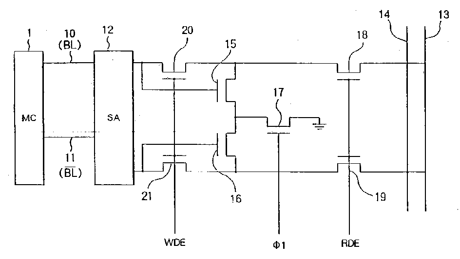
Fig. 4 is the circuit diagram corresponding to the principle configuration of the semiconductor storage of the 1st embodiment of the present invention;
Fig. 5 A to 5C is the view that is used to explain the operation of semiconductor storage shown in Figure 4;
Fig. 6 is the circuit diagram corresponding to the semiconductor storage of the 2nd embodiment of the present invention;
Fig. 7 A to 7M is the timing diagram of operation of the semiconductor storage of key drawing 6;
Fig. 8 is the circuit diagram corresponding to the principle configuration of the semiconductor storage of the 3rd embodiment of the present invention;
Fig. 9 is the circuit diagram corresponding to the principle configuration of the semiconductor storage of the 4th embodiment of the present invention; With
Figure 10 is the circuit diagram corresponding to the principle configuration of the semiconductor storage of the 5th embodiment of the present invention.
Hereinafter with reference to the most preferred embodiment of accompanying drawing detailed description corresponding to semiconductor storage of the present invention.This embodiment relates to dynamic RAM (DRAM), and the storage unit that wherein is used for storing data is included in capacity cell.
Semiconductor storage shown in Figure 4, the composition of memory cell array 1 is: a plurality of storage unit that are used to store data; The voltage of can output reading from this memory cell array 1 and carrying is write voltage to the bit line (BL) 10 of memory cell array 1 and anti-phase bit line (_ BL) 11; Can be amplified to the voltage that these bit lines 10 and anti-phase bit line 11 read and can export the sensor amplifier 12 of these voltages, it can also be write voltage with input via bit line 10 and anti-phase bit line 11 and deliver to memory cell array 1; Can output read voltage and receive the read/write data bus of importing by himself 13 and 14 of writing voltage; Utilize readout gate (transistor) 15 and 16 bit line 10 and anti-phase bit line 11 and finish switch motion by the voltage that sensor amplifier 12 amplifies with readout gate circuit structure; Be arranged on the drain electrode of these readout gates 15 and 16 and the oxide-semiconductor control transistors 17 that the write operation in data between the ground is turned off constantly; Be arranged on readout gate 15 and 16 and data bus 13 and 14 between and read operation constantly and the write operation moment by the reading transistor 18 and 19 of a reading request signal conducting; With, be arranged on readout gate 15 and 16 front one-levels by the written request signal conducting and can write the write transistor 20 and 21 of voltage from what data bus 13 and 14 provided input to sensor amplifier 12.
The read operation of the data shown in Fig. 5 A to 5C constantly, the control signal 1 that delivers to the door place of oxide-semiconductor control transistors 17 becomes high level, these oxide-semiconductor control transistors 17 conductings, this readout gate 15 and 16 drain electrode are via oxide-semiconductor control transistors 17 ground connection, equally, when the reading request signal RDE at the door place that delivers to reading transistor 18 and 19 became high level, this reading transistor 18 and 19 was switched on.
Here, when readout gate 15 conductings, read current is via reading transistor 18, and readout gate 15 and oxide-semiconductor control transistors 17 flow from data bus 13.Equally, when readout gate 16 conductings, read current is via reading transistor 19, and readout gate 16 and oxide-semiconductor control transistors 17 flow from data bus 14. Data bus 13 and 14 voltage are changed by this read current, thereby data are read out.
More specifically be, when the voltage of delivering to readout gate 15 for example and 16 was respectively high level and low level, readout gate 15 conductings and readout gate 16 turn-offed, and electric current flows via reading transistor 18, readout gate 15 and oxide-semiconductor control transistors 17 from data bus 13.Then, the voltage of data bus 13 is because the resistance of data bus 13 etc. are former thereby step-down and final voltage with respect to data bus 14, and the voltage of this data bus 13 becomes low level.
Equally, when the voltage of delivering to readout gate 15 for example and 16 is respectively low level and high level, readout gate 15 turn-offs, readout gate 16 conductings, electric current from data bus 14 via reading transistor 19, readout gate 16 and oxide-semiconductor control transistors 17 flow, and then, the voltage step-down of data bus 14 and the voltage of data bus 13 become high level with respect to the voltage of data bus 14.Like this, be output to data bus 13 and 14 corresponding to the voltage of reading that is stored in the data in the memory cell array 1.
Shown in above-mentioned Fig. 5 C, at the write operation of data constantly, deliver to the control signal 1 of oxide-semiconductor control transistors 17, become low level and oxide-semiconductor control transistors 17 is turn-offed, in other words, this state is to forbid attitude, wherein readout gate 15 and 16 drain electrode do not have ground connection.Equally, a reading request signal RDE who delivers to the door place of reading transistor 18 and 19 becomes high level and reading transistor 18 and 19 conductings.Equally, a written request signal WDE who delivers to the door place of write transistor 20 and 21 becomes high level and write transistor 20 and 21 conductings.
Then, when writing voltage and deliver to data bus 13 and 14, sensor amplifier 12 is through reading transistors 18 and 19 and write the voltage of writing that crystal 20 and 21 receives the inputs of doing it, and this voltage delivered to bit line 10 and anti-phase bit line 11 is write the data of memory cell array 1 to finish.For example, when low level when writing voltage and delivering to writing voltage and delivering to data bus 14 of data bus 13 and high level, this induction amplifier 12 send a high level voltage to bit line 10 with send a low level voltage to anti-phase bit line 11, like this, " 0 " just is stored in the storage unit of memory cell array 1.
Carve at this moment, oxide-semiconductor control transistors 17 is turn-offed, thereby not owing to the source electrode that voltage makes current direction readout gate 15 and 16 of writing from data bus 13 and 14.
Can understand from above-mentioned explanation, this semiconductor storage has such configuration: owing to turn-off in this oxide-semiconductor control transistors 17 of the write operation moment of data, thereby electric current can not flow to readout gate 15 and 16 from data bus 13 and 14, with, wherein because in read and write operation moment common data bus, thereby compare with having the two the semiconductor storage of related art of a read data bus and a write data bus, the area of configuration is lowered.Equally, since write transistor 20 with 21 with reading transistor 18 with 19 with the series connection form with relevant data bus 13 and 14 phase configuration, so the junction capacity of door overlap capacitance and write transistor 20 and 21 does not append to data bus 13 and 14, like this, with write transistor is compared with the semiconductor storage that parallel form is connected the related art of data bus with reading transistor, this electric capacity that appends to data bus 13 and 14 has been lowered, thereby the speed that increases the read and write operation becomes possibility.
It should be noted that to the invention is not restricted to the foregoing description, a kind of configuration that it may adopt is, for example, do not establish anti-phase bit line 11, and only establish bit line 10, and readout gate, oxide-semiconductor control transistors, reading transistor and write transistor.In the case, be based on the read and write operation that electric potential difference between earth potential and the data bus electromotive force is carried out data.Equally, the present invention also is not limited to a kind of DRAM, and it is used for SRAM naturally, short-access storage (flash memory), or similar storage data as electric signal.
Can understand from the above description, in the present invention, semiconductor storage, wherein, transistor with readout gate circuit structure is connected between bit line and the data bus, this source electrode or drain electrode with readout gate circuit structure is connected to earth potential via oxide-semiconductor control transistors, wherein this oxide-semiconductor control transistors is turned off constantly at the write operation of data, with, write transistor comes conducting by the written request signal that is provided in the transistor front one-level with readout gate circuit structure, be arranged between the transistor and data bus with readout gate circuit structure by the reading transistor of this reading request signal conducting constantly constantly and at write operation in read operation, being connected electric capacity and can not appending to data bus of door overlap capacitance and write transistor, thus, read and write operation can with carry out at a high speed and, common data bus when read operation and write operation, thereby compare with relevant prior art, the configuration area can be lowered.
Equally, in semiconductor storage of the present invention, wherein, transistor with readout gate circuit structure is connected between bit line and anti-phase bit line and the data bus, oxide-semiconductor control transistors be arranged on have a readout gate circuit structure and be connected between the source electrode or drain electrode and data bus and ground between bit line and the anti-phase bit line, and turn-off constantly at the write operation of data; Read transistor and be arranged on branch other has between the transistor and data bus of readout gate circuit structure, and read operation constantly and the write operation moment by the reading request signal conducting; Write transistor is arranged on branch and else has the transistorized front one-level of readout gate circuit structure, and conducting and finish switch motion between bit line and anti-phase bit line and reading transistor under written request signal.The junction capacity of door overlap capacitance and write transistor can not append to data bus, therefore, the read and write operation can with carry out at a high speed and, the data bus that uses constantly at read operation and write operation is public, thus the configuration area is lowered.
Fig. 6 is the circuit diagram corresponding to the 2nd embodiment of semiconductor storage of the present invention, wherein represents with same sequence number with the element of those same structures of related art shown in Figure 2.
That is, BLi0, _ BLi0, BLi1, _ BLi1 ... represent that the capable bit line of i is right; WL00 to WL01 ... the expression word line; C00, C01 ... expression belongs to the storage unit with delegation; PRE0 ... the expression pre-charge circuit; SA0 ... the expression sensor amplifier; SW0
A: SW0
BBe can be when operation for the storage unit C0 that connects use, C01 ... with sensor amplifier SA0 ... on-off circuit; BK0, BK1 ... the storage block that expression is divided (storage display); Si0
A: Si0
B, Si1
A: Si1
B... be connected in series storage block bit line or discharge the on-off circuit of storage block bit line of expression; Q1 and Q2 represent the transmission gate by array selecting signal Y control; With DB and _ DB submeter registration according to bus.
Pre-charge circuit PRE0 comprises the N-channel MOS transistor Q3 to Q5 of the gate circuit that contains the pipeline that is connected to precharging signal P.The source electrode of precharge transistor Q3 and Q4 is connected to supply voltage (1/2) V
CcPipeline, and balanced transistor-resistor logic Q5 is connected between the drain electrode of transistor Q3 and Q4, and Q3 and Q4 be connected in bit line to BLi0 and _ BLi0.
Pre-charge circuit PRE0 when providing precharging signal P, is pre-charged to identical electromotive force (1/2V with bit line BLi0 and BLi0
Cc-V
Th), the pre-charge circuit PRE1 of other storage block ... do not draw, but have similar 26S Proteasome Structure and Function.
Storage unit C00 is by N-channel MOS transistor Q
CoBe connected bit line BLi0 and reference potential (for example ground wire) V with the series connection form
pBetween capacitor C
CoConstitute transistor Q
CoGrid be connected to word line WL00.
Similarly, storage unit C01 is by N-channel MOS transistor Q
C1Be connected bit line _ BLi0 and reference potential V with the series connection form
PBetween capacitor C
C1Constitute transistor Q
C1Grid is connected to word line WL01.Other storage unit is not drawn, but all similar structures is arranged.
On-off circuit SW0
AAnd SW0
BBy be respectively inserted into bit line BLi0 and _ BLi0 in and the N-channel MOS transistor Q12 and the Q13 that are connected wherein constitute, the grid of transistor Q12 and Q13 is connected to the pipeline of signal 00.
Sensor amplifier SA0 by with the cross connection of bistable trigger version bit line BLi0 and _ between the pipeline of pipeline between the BLi0 and signal BS0 and inversion signal _ BS0 constituted, wherein, one phase inverter comprises that an interconnective N-channel MOS transistor Q8 of drain and gate and a P channel MOS transistor Q10 and a phase inverter comprise a N-channel MOS transistor Q9 and a P channel MOS transistor Q11.Sensor amplifier SA pins the data of bit line to BLi0 and BLi0, also promptly catches a complementary level, and is amplified.Equally, other storage block BK1 that has similar structures ... induction amplifier do not draw yet.
On-off circuit Si0
A: Si0
BSi1
A: Si1
B... by being inserted in the bit line pairs between other storage block of branch and being connected wherein N-channel MOS transistor Q6
0A: Q6
0B, Q6
1A: Q6
1B... constitute transistor Q6
0AAnd Q6
0BGrid be connected to pipeline and the transistor Q6 of signal 10
1AAnd Q6
1BGrid be connected to the pipeline of signal 11.
Corresponding to signal 10, 11 ... incoming level, the bit line of storage block connects with the string form or discharges.
Gate circuit GT0
AAnd GT0
BBe connected to parallel form and relate to the right on-off circuit Si0 of this bit line
AAnd Si0
B
Gate circuit GT0 is made of a CMOS phase inverter, and this CMOS phase inverter comprises that a P channel MOS transistor Q20 and a N-channel MOS transistor Q21 constitute, and their drain and gate interconnects, at signal 20 (supply voltage V for example
CcLevel) and _ obtain complementary level between the pipeline of 20 (for example ground level).
Then, the tie point of the grid of transistor Q20 and Q21, i.e. gate circuit GT0
AThe tie point of input be connected at storage block BK0 and on-off circuit Si0
BBetween bit line _ BLi0 place and, the drain electrode tie point of transistor Q20 and Q21, promptly the tie point of the output of gate circuit GT0 is connected to the bit line BLi1 place between on-off circuit Si0 and storage block BK1.
Gate circuit GT0
BBe made of a CMOS phase inverter, this CMOS phase inverter comprises a P channel MOS transistor Q20
BWith a N-channel MOS transistor Q21
B, their drain electrode and door interconnect, at signal 20 (supply voltage V for example
CCLevel) and _ obtain complementary level between the pipeline of 20 (for example ground level).
Then, transistor Q20
BAnd Q21
BThe tie point of grid, i.e. gate circuit GT0
BThe tie point of input be connected between storage block BK0 and on-off circuit Si0 bit line BLi0 place and, transistor Q20
BAnd Q21
BThe tie point of drain electrode, i.e. gate circuit GT0
BThe tie point of output be connected at on-off circuit Si0
BAnd the bit line BLi1 between the storage block BK1
BThe place.
Correspondingly, the level as hypothesis bit line BLi0 is V
CCThe level of level and bit line _ BLi0 is a ground level, as for example on-off circuit Si0
AAnd Si0
BWhen being nonconducting state because the signal of the ground level of bit line _ BLi0 is imported into the input end of inverter gate circuit Gi0, then should the next one level of bit line BLi1 of storage display become the level of signal 20, i.e. V
CcLevel.
Equally, because the V of bit line BLi0
CcThe signal of level is transfused to inverter gate circuit Gi0
BInput end, then should the next one level of bit line _ BLi1 of storage display become the level of signal _ 20, i.e. ground level.
Using such method is owing to be connected to on-off circuit Si0 with parallel form
AAnd Si0
BGate circuit Gi0
AAnd Gi0
BExistence, even, if this on-off circuit Si0
AAnd Si0
BBe nonconducting state, then this bit line to BLi0 and _ data of BLi0 can be sent to next bit line to BLi1 and _ BLi1.
Note, have as above-mentioned gate circuit GT0
AAnd GT0
BThe gate circuit GT1 of same structure and function
A: GT1
B... be connected to other on-off circuit Si1 with parallel form
A: Si1
B,
According to the above structure,, will explain next step operation with reference to the timing diagram of Fig. 7 A to Fig. 7 M.It should be noted that existing hypothesis bit line to BLi0 and _ BLi0 quilt charging.
At first, in original state, signal _ RAS and _ CAS the two become high level, this constantly, give charging signals P be in high level and bit line to BLi0 and _ BLi0 given and having been put at high level, as 1/2V
Cc
Next step, row address is latched in the address bus, for example by the negative edge from high level to low level signal _ RAS, the level of selected word line WL00 rises to high level from low level, it should be noted that at this moment and carve that precharging signal P converts low level to from high level.
Along with the level conversion of selected word line LW00 to high level, the transistor Q of this storage unit C00
CoBecome conducting state and be stored in capacitor C
CoIn electric charge be read out on the bit line BLi0 and go.
In the case, the electromotive force that constitutes the right bit line _ BLi0 of bit line with bit line BLi0 is precharge (1/2) V
Cc, initial voltage is higher or low accurate Δ V level than pre-charge voltage, and this accurate Δ V voltage is delivered to bit line BLi0 according to the information that is stored among the storage unit C00.
Then, signal 00 rises to high level and on-off circuit SW0 from low level
AAnd SW0
BRemain on conducting state.
Then, be used to excite the signal BS0 of induction amplifier SA0 to reduce to low level from high level, on the contrary, signal _ BS0 rises to high level from low level.Thus, bit line to BLi0 and _ electric potential difference between the BLi0 amplified by sense amplifier SA0, consequently, the electromotive force that bit line is right, its neutrality line BLi0 remains on supply voltage V
CcLevel, bit line _ BLi0 remains on ground level.
After this, signal 20 rises to high level, and signal _ 20 is arranged on low level, carves at this moment, and signal 10 remains on the low level that it has been, on-off circuit Si0
AAnd Si0
BRemain on nonconducting state.
As above-mentioned, because signal 20 is arranged on high level and signal _ 20 is arranged on low level, if the level of bit line BLi0 is to be in V
CcThe level of level and bit line _ BLi0 is to be in ground level, if even on-off circuit Si0
AAnd Si0
BBe at nonconducting state, because the ground level signal of bit line _ BLi0 is imported into the input end of inverter gate circuit Gi0, so the level of the bit line BLi1 of next storage display becomes the level of signal 20, i.e. V
CcLevel.Equally, because the V of bit line BLi0
CcLevel signal is imported into inverter gate circuit Gi0
BInput end, so the level of the bit line _ BLi1 of next storage display becomes the level of signal _ 20, i.e. ground level.
Using such method, the right electromotive force of bit line is via gate circuit Gi0
A: Gi0
B, Gi1
A: Gi1
B..., be sent to successively on the bit line of input/output end port side.
After this, signal _ CAS reduces to low level from high level, thereby row address is latched, then, signal 00 ... reduce to low level from high level, array selecting signal Y by selectively from low level rise to high level and, the information of reading from storer be sent to data bus DB and _ DB.
As explained above, corresponding to present embodiment, amplify the gate circuit Gi0 of this signal to I/O door direction from bit line
A: Gi0
B... be connected to the on-off circuit Si0 that is used to connect bit line with parallel form
A: Si0
B..., this is used to connect the on-off circuit Si0 of bit line
A: Si0
B... after read operation, open immediately, and gate circuit Gi0
A: Gi0
B... be excited simultaneously, thereby bit line signal can not reduce the driving force of sensor amplifier to be read out at a high speed.
It should be noted that even if so constitutes that the execution of i.e. read operation is until the electromotive force of selected bit line is reached for to finish rewrites in storage unit till the necessary electromotive force, then, this bit line signal amplifies gate circuit Gi0
A: Gi0
B... be excited, this also can obtain and the similar effect of above-mentioned effect.
Equally, before bit line potentials reached predetermined voltage fully, this was used to connect the on-off circuit Si0 of bit line
A: Si0
B... be opened and at this synchronization gate circuit Gi0
A: Gi0
B... be excited, thereby it also can further increase read operation speed.
But under one situation of back, read signal output to data bus DB and _ DB after, must open row and select door, be closed in bit line and the on-off circuit between the sensor amplifier that belongs to selected storage block and from the sensor amplifier to the bit line, provide for rewriteeing necessary voltage.
Equally, in the present embodiment, for the composition explanation of the set sensor amplifier of each storage block (storage array), but need not say that the present invention can provide a kind of and be referred to as to share-sense amplifier system, in this system, the shared sensor amplifier of for example per two storage arrays that adjoin.
Fig. 8 is the circuit diagram corresponding to the principle configuration of the 3rd embodiment of semiconductor storage of the present invention.
The difference of present embodiment and above-mentioned the 1st embodiment ascribes to, and this phase inverter that is used as gate circuit is arranged in the right only line of bit line.
In this situation, the information from storage block BK0 to storage block BK1 is sent to bit line BLi1 from bit line _ BLi0.
Impact damper from bit line BLi1 to output port connected, the connection of this phase inverter must alternative inversion.
Introduce in the case, if data bus DB and _ DB just is being preset to/intermediate value of negative supply voltage and data bus DB and _ DB is read out amplification in the time that lags behind a little of the rising edge from array selecting signal Y, this array selecting signal Y is the signal that excites the ABC of Q1 of transmission and Q2 selectively, that is a signal that obtains by for example CAS signal delay.
Owing to adopt such configuration, a kind of advantage also just arranged therein.In addition, except the effect of the foregoing description, promptly this bit line discharges stream that is used for complete loop can be lowered half.
Fig. 9 is the circuit diagram corresponding to the principle configuration of the 4th embodiment of semiconductor storage of the present invention.
The distinctive points of present embodiment and above-mentioned the 2nd embodiment is that gate circuit Gi0 is made of single phase inverter, but constitute by two cascaded inverters IV1 and IV2, equally, its output is not to be connected in bit line _ BLi0 but the input that is connected in the gate circuit Gi0 of bit line BLi1 is connected in bit line BLi0.
Corresponding to present embodiment, on data line, read amplification not necessarily, thereby it may reduce the discharge current of bit line.
Figure 10 is the circuit diagram corresponding to the principle configuration of the 5th embodiment of semiconductor storage of the present invention.
In Figure 10, TF1 and TF2 show it is to be interconnected and the transmission gate that constitutes by the drain electrode of N-channel MOS transistor and P channel MOS transistor and source electrode; DSA is a differential scale-up version sensor amplifier; Q20 is the N-channel MOS transistor that is used for gate circuit.
Present embodiment is a kind of structure of a corresponding instrument, and the bit line of this instrument is not to be pre-charged to 1/2V
Cc, but be pre-charged to V
CcLevel.
That is, in this instrument, the composition of its structure is: bit line is given is charged to supply voltage V
CcThe high level of level; This transistor Q20 only, is just driven by sensor amplifier SA when being transmitted in low level (ground level); With, the bit line BLi1 of next stage being drawn to ground level.
Equally, in the present embodiment, can obtain those similar effects in the foregoing description.
Explain as above that corresponding to of the present invention it can increase the speed of read operation and reduce the charging current of bit line and suppress power consumption in the identical moment.
Claims (2)
Applications Claiming Priority (6)
| Application Number | Priority Date | Filing Date | Title |
|---|---|---|---|
| JP328340/93 | 1993-12-24 | ||
| JP5328340A JPH07182865A (en) | 1993-12-24 | 1993-12-24 | Semiconductor memory device |
| JP328340/1993 | 1993-12-24 | ||
| JP137315/1994 | 1994-06-20 | ||
| JP6137315A JPH087564A (en) | 1994-06-20 | 1994-06-20 | Semiconductor memory device |
| JP137315/94 | 1994-06-20 |
Related Child Applications (1)
| Application Number | Title | Priority Date | Filing Date |
|---|---|---|---|
| CNB971231184A Division CN1149580C (en) | 1993-12-24 | 1997-11-14 | DRAM |
Publications (2)
| Publication Number | Publication Date |
|---|---|
| CN1115100A CN1115100A (en) | 1996-01-17 |
| CN1055346C true CN1055346C (en) | 2000-08-09 |
Family
ID=26470668
Family Applications (2)
| Application Number | Title | Priority Date | Filing Date |
|---|---|---|---|
| CN94120723A Expired - Lifetime CN1055346C (en) | 1993-12-24 | 1994-12-23 | Dynamic random access memory |
| CNB971231184A Expired - Lifetime CN1149580C (en) | 1993-12-24 | 1997-11-14 | DRAM |
Family Applications After (1)
| Application Number | Title | Priority Date | Filing Date |
|---|---|---|---|
| CNB971231184A Expired - Lifetime CN1149580C (en) | 1993-12-24 | 1997-11-14 | DRAM |
Country Status (3)
| Country | Link |
|---|---|
| US (1) | US5515315A (en) |
| KR (1) | KR950020734A (en) |
| CN (2) | CN1055346C (en) |
Families Citing this family (9)
| Publication number | Priority date | Publication date | Assignee | Title |
|---|---|---|---|---|
| KR100244247B1 (en) * | 1997-04-09 | 2000-02-01 | 김영환 | Sensing circuit |
| JP3360717B2 (en) * | 1997-09-29 | 2002-12-24 | 日本電気株式会社 | Dynamic semiconductor memory device |
| KR100301822B1 (en) * | 1999-07-21 | 2001-11-01 | 김영환 | Sensing amp of nonvolatile ferroelectric memory device |
| US7349266B2 (en) * | 2004-06-10 | 2008-03-25 | Freescale Semiconductor, Inc. | Memory device with a data hold latch |
| JP5337108B2 (en) * | 2009-08-10 | 2013-11-06 | セイコーインスツル株式会社 | Memory circuit and voltage detection circuit having the same |
| TW201142869A (en) * | 2010-02-09 | 2011-12-01 | Samsung Electronics Co Ltd | Memory device from which dummy edge memory block is removed |
| US11145923B2 (en) * | 2016-10-13 | 2021-10-12 | Prologium Technology Co., Ltd. | Battery structure |
| US11145924B2 (en) * | 2017-10-09 | 2021-10-12 | Prologium Technology Co., Ltd. | Battery structure |
| CN112018118B (en) * | 2020-07-21 | 2024-08-06 | 长江存储科技有限责任公司 | 3D memory device, memory structure thereof and control method of memory structure |
Citations (1)
| Publication number | Priority date | Publication date | Assignee | Title |
|---|---|---|---|---|
| US4730280A (en) * | 1984-11-20 | 1988-03-08 | Fujitsu Limited | Semiconductor memory device having sense amplifiers with different driving abilities |
Family Cites Families (3)
| Publication number | Priority date | Publication date | Assignee | Title |
|---|---|---|---|---|
| DE3039997A1 (en) * | 1980-10-23 | 1982-06-03 | Bayer Ag, 5090 Leverkusen | PHOSPHONOHYDROXYACETONITRILE, A METHOD FOR THE PRODUCTION THEREOF AND ITS USE AS AN INTERMEDIATE PRODUCT FOR THE PRODUCTION OF MEDICINAL PRODUCTS |
| JPS62123093A (en) * | 1985-11-22 | 1987-06-04 | Nec Corp | Mounting of substrate on molecular beam epitaxial growth apparatus |
| JPH06215564A (en) * | 1993-01-13 | 1994-08-05 | Nec Corp | Semiconductor storage device |
-
1994
- 1994-12-20 US US08/360,007 patent/US5515315A/en not_active Expired - Lifetime
- 1994-12-22 KR KR1019940035896A patent/KR950020734A/en not_active Withdrawn
- 1994-12-23 CN CN94120723A patent/CN1055346C/en not_active Expired - Lifetime
-
1997
- 1997-11-14 CN CNB971231184A patent/CN1149580C/en not_active Expired - Lifetime
Patent Citations (1)
| Publication number | Priority date | Publication date | Assignee | Title |
|---|---|---|---|---|
| US4730280A (en) * | 1984-11-20 | 1988-03-08 | Fujitsu Limited | Semiconductor memory device having sense amplifiers with different driving abilities |
Also Published As
| Publication number | Publication date |
|---|---|
| CN1115100A (en) | 1996-01-17 |
| KR950020734A (en) | 1995-07-24 |
| US5515315A (en) | 1996-05-07 |
| CN1185006A (en) | 1998-06-17 |
| CN1149580C (en) | 2004-05-12 |
Similar Documents
| Publication | Publication Date | Title |
|---|---|---|
| US7342826B2 (en) | Semiconductor device | |
| CN1196137C (en) | Digit line setting and discharge circuit for programming nonvolatile memory | |
| CN101599300B (en) | Static Random Access Memory Using Boosted Voltage | |
| US4661928A (en) | Output buffer in which inductive noise is suppressed | |
| US6826081B2 (en) | Nonvolatile semiconductor memory device, nonvolatile semiconductor memory device-integrated system, and defective block detecting method | |
| US7379345B2 (en) | Nonvolatile semiconductor memory device that achieves speedup in read operation | |
| US6795346B2 (en) | Non volatile memory and data processor | |
| CN1591684A (en) | Semiconductor memory device | |
| US6154405A (en) | Semiconductor memory device having a dummy cell resetting the bit lines to a reset potential that is based on data read in a previous read data | |
| KR20000020558A (en) | Input and output line precharging circuit of semiconductor memory and method for using the same | |
| US8644095B2 (en) | Input-output line sense amplifier having adjustable output drive capability | |
| CN1185006A (en) | Dynamic random access storage | |
| US7154784B2 (en) | Flash memory with reduced size and method for accessing the same | |
| CN107527639A (en) | Memory reading circuitry and its read method | |
| JPH06139776A (en) | Semiconductor memory device | |
| US5295104A (en) | Integrated circuit with precharged internal data bus | |
| US6385108B2 (en) | Voltage differential sensing circuit and methods of using same | |
| US6597201B1 (en) | Dynamic predecoder circuitry for memory circuits | |
| JP3843486B2 (en) | Nonvolatile semiconductor memory device | |
| JP4294977B2 (en) | Nonvolatile storage device | |
| TWI281159B (en) | Sense out circuit for single-bitline semiconductor memory device | |
| JPH07220477A (en) | Semiconductor memory device | |
| JP4012151B2 (en) | Nonvolatile semiconductor memory device | |
| JP4604436B2 (en) | Semiconductor memory device and data read method thereof | |
| JP2011187141A (en) | Transfer circuit and nonvolatile semiconductor memory device using the same |
Legal Events
| Date | Code | Title | Description |
|---|---|---|---|
| C06 | Publication | ||
| PB01 | Publication | ||
| C10 | Entry into substantive examination | ||
| SE01 | Entry into force of request for substantive examination | ||
| C14 | Grant of patent or utility model | ||
| GR01 | Patent grant | ||
| C17 | Cessation of patent right | ||
| CX01 | Expiry of patent term |
Expiration termination date: 20141223 Granted publication date: 20000809 |