The present application is a divisional application of chinese patent application entitled method for manufacturing vapor deposition mask and method for manufacturing organic semiconductor element, filed by japan printing press, 2013, year 01, month 11, and application No. 201380005299.3.
Detailed Description
Hereinafter, a method for manufacturing a vapor deposition mask according to the present invention will be described in detail with reference to the drawings. In the following description, first, the process will be mainly described, and the description of the material and the like will be collectively made when the vapor deposition mask manufactured by the manufacturing method is described.
(first production method)
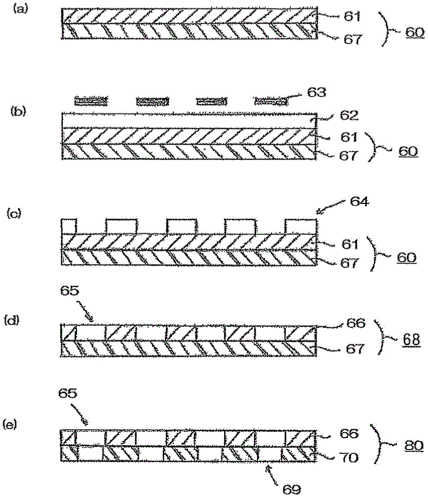
Fig. 1 is a process diagram for explaining a first method for manufacturing a vapor deposition mask according to the present invention. FIGS. 1(a) to (e) are sectional views.
As shown in fig. 1(a), a resin-layer-provided metal plate 60 having a resin layer 67 provided on one surface of a metal plate 61 is prepared. Here, the method for preparing the metal plate with a resin layer 60 is not particularly limited, and a commercially available metal plate with a resin layer 60 may be purchased, or a metal plate with a resin layer 60 may be formed by providing a resin layer on the surface of the metal plate. As a method of providing a resin layer on the surface of the metal plate, for example, a coating liquid containing a resin to be a resin layer is applied to the metal plate and dried, thereby obtaining a metal plate 60 with a resin layer. Instead of this method, a resin plate may be bonded to a metal plate to obtain a metal plate with a resin layer. As a method for bonding the metal plate and the resin plate, for example, various adhesives may be used, or a resin plate having self-adhesiveness may be used. Further, it is known that a so-called aging period needs to be provided until the shape of the resin is stabilized because the resin changes with time in a certain period after the formation. Since the commercially available metal plate with a resin layer 60 is considered to have passed through a so-called aging period, it is preferable to use the commercially available metal plate with a resin layer from the viewpoint of yield.
Next, a metal mask 68 with a resin layer is formed on the metal plate 61 of the metal plate 60 with a resin layer by forming a slit penetrating only the metal plate. The step in the method is not particularly limited, and any step may be used as long as a desired slit can be formed only in the metal mask. The resin layer-provided metal mask 68 referred to in the present specification means a structure in which a slit is formed in the metal plate of the resin layer-provided metal plate 60.
Fig. 1(b) to (d) show an example of a process for forming the metal mask 68 with a resin layer. As shown in fig. 1(b), a resist material 62 is applied to the surface of the resin layer-equipped metal plate 60 on which the resin layer 67 is not provided, and the resist material is masked with a mask 63 having a slit pattern formed thereon, and exposed and developed. As a result, as shown in fig. 1(c), a resist pattern 64 is formed on the surface of the metal plate 67. Then, the resist pattern 64 is used as an etching resist mask, and only the metal plate 60 is etched, and after the etching is completed, the resist pattern is removed by washing. As a result, as shown in fig. 1 d, a metal mask 66 (metal mask with resin layer 68) in which slits 65 are formed only in the metal plate 67 can be obtained.
The method of masking the resist material is not particularly limited, and the resist material 62 may be applied only to the surface of the resin-layer-provided metal plate 60 on which the resin layer 67 is not provided as shown in fig. 1(b), or the resist material 62 may be applied to both surfaces of the resin-layer-provided metal plate 60 (not shown). Further, a dry film method in which a dry film resist is bonded to the surface of the metal plate with a resin layer 60 on which the resin layer 67 is not provided, or to both surfaces of the metal plate with a resin layer 60 can also be used. The method for applying the resist material 62 is not particularly limited, and when the resist material 62 is applied only to the surface of the metal plate 60 with a resin layer on which the resin layer 67 is not provided, a spin coating method or a spray coating method can be used. On the other hand, when the long sheet-like metal plate 60 with a resin layer is used, a dip coating method or the like capable of applying a resist material in a roll-to-roll manner is preferably used. In the dip coating method, the resist material 62 is applied to both surfaces of the metal plate with resin layer 60.
As the resist material, a material having good handling property and a desired resolution is preferably used. The etching material used in the etching process is not particularly limited, and a known etching material may be appropriately selected.
The etching method of the metal plate 60 is not particularly limited, and examples thereof include a wet etching method such as a spray etching method in which an etching material is sprayed from a spray nozzle at a predetermined spray pressure, a dip etching method in which the etching material is immersed in an etching solution filled with the etching material, and a spin etching method in which the etching material is dropped, and a dry etching method using gas, plasma, or the like.
Next, a resin mask 70 is formed by irradiating the metal plate 68 with laser light from the metal mask 66 side through the slit 65, and forming a plurality of rows (2 or more) of openings 69 corresponding to a pattern to be vapor-deposited in the resin layer 67 in a vertical and horizontal manner. The laser device used here is not particularly limited, and a conventionally known laser device may be used. This makes it possible to obtain a vapor deposition mask 80 as shown in fig. 1 (e). In the present specification, the pattern to be formed by vapor deposition means a pattern to be formed using the vapor deposition mask, and for example, when the vapor deposition mask is used for forming an organic layer of an organic electroluminescent element, the pattern is in the shape of the organic layer. Hereinafter, the same applies to the manufacturing method of the other embodiments.
(second production method)
Fig. 2 is a process diagram for explaining a second method for manufacturing a vapor deposition mask according to the present invention. In addition, fig. 2(a) to (e) are sectional views.
In the first manufacturing method shown in fig. 1, the etching pattern 64 used as an etching mask in forming the metal mask 66 is removed, but may be left as it is as shown in fig. 2(d) and 2(e) without removing it. The other steps, that is, (a) to (c) of fig. 2, are the same as (a) to (c) of fig. 1, and therefore, the description thereof is omitted here.
In the first and second manufacturing methods, the metal mask 66 (the metal mask 68 with the resin layer) may be formed and then the metal mask 68 with the resin layer may be fixed to the metal-containing frame, that is, between fig. 1 and fig. 2(d) and (e). In this way, by fixing the vapor deposition mask to the frame at a stage before forming the openings of the resin mask 70 corresponding to the pattern shape to be finally produced by vapor deposition, the mounting error occurring when the vapor deposition mask is fixed to the frame can be made zero. In the conventional method, the metal mask defining the opening is fixed to the frame while being stretched, and therefore the accuracy of the opening position coordinates is lowered.
When the openings 69 are provided in the resin layer of the metal mask with resin layer 68 fixed to the housing by the laser processing method, a reference plate on which a pattern to be vapor-deposited, that is, a pattern corresponding to the openings 69 to be formed is provided in advance may be prepared, and laser irradiation corresponding to the pattern of the reference plate may be performed from the metal mask 66 side in a state where the reference plate is bonded to the surface of the metal mask with resin layer 68 on the side where the metal mask 66 is not provided. According to this method, the openings 69 can be formed in the resin layer 68 in a state where the reference plate patterns bonded to the metal mask with resin layer 68 are observed and laser irradiation is performed so as to face each other (こう to わせ), and the resin mask 70 having the openings 69 with high definition and extremely high dimensional accuracy can be formed. In addition, in this method, since the opening 69 is formed in a state of being fixed to the frame, it is possible to form a vapor deposition mask having not only high dimensional accuracy but also excellent positional accuracy.
In addition, in the case of using the above method, it is necessary to be able to recognize the pattern of the reference plate from the metal mask 66 side through the resin layer 67 by a laser irradiation device or the like. The resin layer 67 needs to have a structure having transparency when it has a certain thickness, but as described later, when it is formed to have a preferable thickness in consideration of the influence of shading, for example, a thickness of about 3 to 25 μm, the pattern of the reference plate can be recognized even with a colored resin layer.
The method of bonding the resin layer and the reference plate is not particularly limited, and for example, in the case where the metal mask 66 is a magnetic material, a magnet or the like is disposed behind the reference plate, and the resin layer 67 and the reference plate are bonded by being attracted. In addition, bonding can be performed by an electrostatic adsorption method or the like. Examples of the reference plate include a TFT substrate having a predetermined pattern, a photomask, and the like.
According to the first and second manufacturing methods of the present invention, even when both are increased in size, a vapor deposition mask that can satisfy both high definition and light weight can be manufactured with high yield. In addition, according to one embodiment of the present invention, the positional accuracy of the frame and the vapor deposition mask 100 can be improved. In addition, by forming the opening 69 using the reference plate, the opening 69 can be formed with excellent dimensional accuracy.
Specifically, in the manufacturing method of the present invention, the vapor deposition mask 100 in which the resin mask 70 and the metal mask 66 are laminated is manufactured. Here, on the assumption that the thickness of the entire vapor deposition mask is the same, the mass of the vapor deposition mask 100 of the present invention is reduced by replacing a part of the metal material of the conventionally known vapor deposition mask with the resin material, as compared with the mass of the vapor deposition mask made of only the conventionally known metal, by comparing the mass of the vapor deposition mask 100 manufactured by the manufacturing method of the present invention with the mass of the vapor deposition mask made of only the conventionally known metal. Further, although a vapor deposition mask made of only a metal is used, the thickness of the vapor deposition mask needs to be reduced in order to reduce the weight, when the thickness of the vapor deposition mask is reduced, the vapor deposition mask may be deformed or the durability may be reduced when the vapor deposition mask is increased in size. On the other hand, according to the vapor deposition mask of the present invention, even when the vapor deposition mask is deformed in an increase in size or the thickness of the entire vapor deposition mask is increased to satisfy durability, the weight can be reduced compared to a vapor deposition mask formed only of a metal due to the presence of the resin mask 70.
In the manufacturing method of the present invention, since the resin mask 70 can be obtained by irradiating the resin layer 67 capable of forming the high-definition openings with the laser light as compared with the metal material, the vapor deposition mask 100 having the high-definition openings 69 can be manufactured.
(thinning Process)
In the manufacturing method of the present invention, the thinning step may be performed between the steps described above or after the steps. This step is an arbitrary step of the manufacturing method of the present invention, and is a step of optimizing the thickness of the metal mask 66 or the thickness of the resin mask 70. The preferred thickness of the metal mask 66 or the resin mask 70 may be set as appropriate within a preferred range described later, and a detailed description thereof will be omitted.
For example, when a metal plate with a resin layer 60 having a certain thickness is used, excellent durability and transportability can be provided when the vapor deposition mask 100 produced by the above-described production method is transported in the production process when the metal plate with a resin layer 60 or the metal mask with a resin layer 68 is transported. On the other hand, in order to prevent the occurrence of a shadow or the like, the thickness of the vapor deposition mask 100 obtained by the production method of the present invention is preferably an optimum thickness. The thinning step is a step useful in the case where the thickness of the vapor deposition mask 100 is optimized while satisfying durability and transportability between manufacturing steps or after the steps.
The thinning of the metal plate 61 or the metal mask 66 to be the metal mask 66, that is, the optimization of the thickness of the metal mask can be achieved by etching the surface of the metal plate 61 not in contact with the resin layer or the surface of the metal mask 66 not in contact with the resin layer 67 or the resin mask 70 using an etching material capable of etching the metal plate 61 or the metal mask 66 after the above-described steps or steps.
Similarly, the resin layer 67 or the resin mask 70 to be the resin mask 70 is thinned, that is, the thicknesses of the resin layer 67 and the resin mask 70 are optimized, and after the above-described steps or the above-described steps, the surface of the resin layer 70 not in contact with the metal plate 61 or the metal mask 66 or the surface of the resin layer 70 not in contact with the metal mask 66 is etched by using an etching material capable of etching the material of the resin layer 67 or the resin mask 70. After the vapor deposition mask 100 is formed, the thicknesses of both the metal mask 66 and the resin mask 70 can be optimized by etching both the masks.
In the thinning step, the etching material for etching the resin layer 67 or the resin mask 70 may be appropriately set according to the resin material of the resin layer 67 or the resin mask 70, and is not particularly limited. For example, when a polyimide resin is used as a resin material of the resin layer 67 or the resin mask 70, an alkaline aqueous solution in which sodium hydroxide or potassium hydroxide is dissolved, hydrazine hydrate, or the like can be used as an etching material. As the etching material, a commercially available product can be used as it is, and as the etching material for polyimide resin, TPE3000 manufactured by tokyo corporation and the like can be used.
(vapor deposition mask produced by the first production method)
Fig. 3(a) is a front view of the vapor deposition mask manufactured by the first manufacturing method, as viewed from the metal mask side, and fig. 3(b) is an enlarged cross-sectional view of the vapor deposition mask 100 manufactured by the first manufacturing method. The figure shows the ratio of the metal mask to the entire metal mask in order to emphasize the gap provided in the metal mask and the opening provided in the vapor deposition mask. For convenience of explanation, in the embodiment shown in fig. 3 to 6, the metal mask mark is denoted by 10, the resin mask mark is denoted by 20, the metal mask 10 can be directly replaced with the metal mask 66 described in the manufacturing method of the present invention, and the resin mask 20 can be directly replaced with the metal mask 70 described in the manufacturing method of the present invention.
As shown in fig. 3, the vapor deposition mask 100 manufactured by the first manufacturing method of the present invention is configured by stacking a metal mask 10 provided with slits 15 and openings 25 positioned on the surface of the metal mask 10 (the lower surface of the metal mask 10 in the case shown in fig. 3 (b)) and arranged in a plurality of rows and columns in a vertical and horizontal manner so as to correspond to a pattern to be vapor deposited. Hereinafter, each of the methods will be described specifically.
(resin mask)
The resin mask 20 is made of resin, and as shown in fig. 3, a plurality of rows of openings 25 corresponding to a pattern to be vapor-deposited are arranged in a row and column at positions overlapping the slits 15. In the present invention, the example in which the plurality of rows of openings are arranged vertically and horizontally has been described, but the openings 25 may be provided at positions overlapping the slits, and when only one row of openings is arranged in the longitudinal direction or the lateral direction of the slits 15, the openings 25 may be provided at positions overlapping the slits 15 in the row.
The resin mask 20 can be used by appropriately selecting a conventionally known resin material, and the material is not particularly limited, and a material which can form the high-definition openings 25 by laser processing or the like, and which has a small thermal or temporal dimensional change rate or moisture absorption rate and is lightweight is preferably used. Examples of such a material include polyimide resin, polyamide-imide resin, polyester resin, polyethylene resin, polyvinyl alcohol resin, polypropylene resin, polycarbonate resin, polystyrene resin, polyacrylonitrile resin, ethylene-vinyl acetate copolymer resin, ethylene-vinyl alcohol copolymer resin, ethylene-methacrylic acid copolymer resin, polyvinyl chloride resin, polyvinylidene chloride resin, cellophane, ionomer resin, and the like. Among the above-mentioned materials, a resin material having a thermal expansion coefficient of 16 ppm/DEG C or less is preferable, and a resin material having a moisture absorption rate of 1.0% or less is preferable, and a resin material having both of these conditions is particularly preferable. Therefore, since the resin layer 67 in fig. l and 2 will be the resin mask 20 in the future, for example, a resin layer made of a preferable resin material in the above-described example is preferably used.
The thickness of the resin mask 20 is not particularly limited, but when vapor deposition is performed using the vapor deposition mask of the present invention, it is preferable to make the resin mask 20 as thin as possible in order to prevent the occurrence of an insufficient vapor deposition portion, that is, a vapor deposition portion having a film thickness smaller than a desired vapor deposition film thickness, that is, a so-called shadow, in a pattern to be vapor deposited. However, when the thickness of the resin mask 20 is less than 3 μm, defects such as pinholes tend to occur, and the risk of deformation or the like increases. On the other hand, if it exceeds 25 μm, shading occurs. In view of this point, the thickness of the resin mask 20 is preferably 3 μm or more and 25 μm or less. By setting the thickness of the resin mask 20 within this range, it is possible to reduce the risk of defects such as pinholes, deformation, and the like, and to effectively prevent the occurrence of shadows. In particular, by forming the thickness of the resin mask 20 to be 3 μm or more and 10 μm or less, more preferably 4 μm or more and 8 μm or less, the influence of the shadow can be more effectively prevented when forming a high-definition pattern exceeding 300 ppi. Therefore, the resin layer 67 in fig. 1 and 2 is preferably formed to have the above thickness since it will be the resin mask 20 in the future. The resin layer 67 may be bonded to the metal plate via an adhesive layer or an adhesive layer, or the resin layer 67 and the metal plate may be directly bonded, but when the resin layer and the metal plate are bonded via an adhesive layer or an adhesive layer, the total thickness of the resin layer 67 and the adhesive layer or the resin layer 67 and the adhesive layer is preferably set to be in the range of 3 μm to 25 μm in consideration of the above-described shading.
The shape and size of the opening 25 are not particularly limited, and may be any shape and size according to the pattern to be formed by vapor deposition. As shown in fig. 2(a), the pitch P1 in the lateral direction or the pitch P2 in the vertical direction of the adjacent openings 25 can be set as appropriate according to the pattern to be produced by vapor deposition. Therefore, in the case of forming the openings by laser irradiation in fig. 1 and 2, the pitches P1 and P2 may be appropriately designed.
The position where the opening 25 is provided and the number of the openings 25 are not particularly limited, and one opening may be provided at a position overlapping the slit 15, or a plurality of openings (2 or more) may be provided in the longitudinal direction or the transverse direction. For example, as shown in fig. 5(a), when the slit extends in the longitudinal direction, two or more opening portions 25 may be provided in the lateral direction so as to overlap with the slit 15.
The cross-sectional shape of the openings 25 is not particularly limited, and the end surfaces of the resin mask that form the openings 25 and face each other may be substantially parallel to each other, but as shown in fig. 3(b) or 4, the cross-sectional shape of the openings 25 is preferably a shape that spreads toward the vapor deposition source. In other words, it is preferable to have a tapered surface expanding toward the metal mask 10 side. By forming the cross-sectional shape of the opening 25 in this configuration, it is possible to prevent the shadow from being generated in the pattern to be formed by vapor deposition when vapor deposition is performed using the vapor deposition mask of the present invention. The taper angle θ can be appropriately designed in consideration of the thickness of the resin mask 20, but it is preferable that the angle connecting the lower bottom end of the opening of the resin mask and the upper bottom end of the opening of the same resin mask is in the range of 25 ° to 65 °. In particular, in this range, an angle smaller than the deposition angle of the deposition machine used is preferable. In fig. 3(b) or 4, the end surface 25a forming the opening 25 has a linear shape, but is not limited thereto, and may have a curled shape protruding outward, that is, the entire shape of the opening 25 may be bowl-shaped. The opening 25 having such a cross-sectional shape can be formed by appropriately adjusting the irradiation position of the laser beam and the irradiation energy of the laser beam, or by performing laser irradiation in multiple stages (2 stages or more) in which the irradiation position is changed stepwise.
In the present invention, since the resin mask 20 is used as the structure of the vapor deposition mask 100, when vapor deposition is performed using the vapor deposition mask 10, extremely high heat is applied to the openings 25 of the resin mask 20, gas is generated from the end surfaces 25a (see fig. 3) of the resin mask 20 where the openings 25 are formed, and the degree of vacuum or the like in the vapor deposition device is reduced. Therefore, in view of this point, as shown in fig. 3, it is preferable that a barrier layer 26 is provided on an end face 25a of the resin mask 20 where the opening 25 is formed. By forming the barrier layer 26, it is possible to prevent gas from being generated from the end face 25a of the resin mask 20 where the opening 25 is formed.
The barrier layer 26 may be a thin film layer of inorganic oxide, inorganic nitride, metal, or an evaporated layer. As the inorganic oxide, aluminum, or oxides of silicon, indium, tin, and magnesium can be used, and as the metal, aluminum or the like can be used. The thickness of the barrier layer 26 is preferably about 0.05 μm to 1 μm. Therefore, in the manufacturing method of the present invention described in fig. l and 2, the step of forming the barrier layer 26 as described above may be performed after the vapor deposition mask 80 is obtained.
Further, the barrier layer preferably covers the surface on the vapor deposition source side of the resin mask 20. The barrier property is further improved by covering the vapor deposition source side surface of the resin mask 20 with the barrier layer 26. The barrier layer is preferably formed by various PVD methods or CVD methods in the case of an inorganic oxide or an inorganic nitride. In the case of metal, it is preferably formed by a vacuum evaporation method. The surface on the vapor deposition source side of the resin mask 20 described here may be the entire surface on the vapor deposition source side of the resin mask 20, or may be a portion exposed only from the metal mask on the surface on the vapor deposition source side of the resin mask 20.
(Metal mask)
The metal mask 10 is made of metal, and when viewed from the front of the metal mask 10, a plurality of rows of slits 15 extending in the longitudinal direction or the transverse direction are arranged at positions overlapping the openings 25, in other words, at positions arranged in all the openings 25 of the resin mask 20. In fig. 3, the slits 15 extending in the longitudinal direction of the metal mask 10 are arranged continuously in the lateral direction. In the present invention, the slits 15 extending in the longitudinal direction or the transverse direction are arranged in a plurality of rows, but the slits 15 may be arranged only in one row in the longitudinal direction or the transverse direction.
The width W of the slit 15 is not particularly limited, but is preferably designed to be shorter than the pitch between the adjacent openings 25. Specifically, as shown in fig. 2(a), in the case where the slit 15 extends in the longitudinal direction, the width W in the lateral direction of the slit 15 is preferably shorter than the pitch P1 of the opening portions 25 adjacent in the lateral direction. Similarly, although not shown, in the case where the slits 15 extend in the transverse direction, the longitudinal width of the slits 15 is preferably shorter than the pitch P2 of the slits 25 adjacent in the longitudinal direction. On the other hand, the longitudinal length L of the slit 15 when extending in the longitudinal direction is not particularly limited, and may be appropriately designed according to the longitudinal length of the metal mask 1 and the position of the opening 25 provided in the resin mask 20. Therefore, in the manufacturing method of the present invention described with reference to fig. 1 and 2, the metal plate is preferably etched as described above.
Further, the slit 15 continuously extending in the longitudinal or transverse direction may be divided into a plurality of pieces by the bridge 18 as shown in fig. 5 (b). Fig. 5b is a front view of the vapor deposition mask 100 as viewed from the metal mask 10 side, and shows an example in which one slit 15 continuously extending in the longitudinal direction shown in fig. 3 a is divided into a plurality of slits ( slits 15a and 15b) by the bridge 18. The width of the bridge 18 is not particularly limited, but is preferably about 5 μm to 20 μm. By setting the width of the bridge 18 in this range, the rigidity of the metal mask 10 can be effectively improved. The position of the bridge 18 is not particularly limited, and the bridge 18 is preferably disposed so that the divided slits overlap two or more openings 25.
The cross-sectional shape of the slit 15 formed in the metal mask 10 is not particularly limited, but is preferably a shape spreading toward the vapor deposition source as shown in fig. 3, similarly to the opening 25 of the resin mask 20. Therefore, in the manufacturing method of the present invention described with reference to fig. l and 2, it is preferable that the metal plate is etched so as to have the above-described cross-sectional shape.
The material of the metal mask 10 is not particularly limited, and conventionally known materials can be appropriately selected and used in the field of vapor deposition masks, and examples thereof include metal materials such as stainless steel, iron-nickel alloys, and aluminum alloys. Among them, an iron-nickel alloy, i.e., an invar material, is suitably used because it is less deformed by heat.
When the vapor deposition mask 100 of the present invention is used to perform vapor deposition on a substrate, the metal mask 10 is preferably formed of a magnetic material when it is necessary to arrange a magnet or the like behind the substrate and attract the vapor deposition mask 100 in front of the substrate by magnetic force. Examples of the magnetic metal mask 10 include pure iron, carbon steel, W steel, Cr steel, Co steel, KS steel, MK steel, NKS steel, Cunico steel, and Al — Fe alloy. In the case where the material itself forming the metal mask 10 is not a magnetic body, the metal mask 10 may be provided with magnetism by dispersing the powder of the magnetic body in the material.
The thickness of the metal mask is not particularly limited, but is preferably about 5 μm to 100 μm. When the thickness of the metal mask 10 is preferably small in consideration of prevention of shading at the time of vapor deposition, and when it is thinner than 5 μm, the risk of cracking and deformation increases and handling may be difficult. However, in the present invention, since the metal mask 10 and the resin mask 20 are integrated, the risk of cracking and deformation can be reduced even when the thickness of the metal mask 10 is very small, i.e., 5 μm or more, and the metal mask can be used. When the thickness is larger than 100 μm, shading can be generated, which is not preferable. Therefore, in the manufacturing method of the present invention described with reference to fig. 1 and 2, it is preferable to prepare a metal plate with a resin layer in consideration of these circumstances.
The relationship between the occurrence of the shadow and the thickness of the metal mask 10 will be specifically described below with reference to fig. 6(a) to 6 (c). As shown in fig. 6(a), when the thickness of the metal mask 10 is small, the vapor deposition material released from the vapor deposition source to the vapor deposition object reaches the vapor deposition object through the slit 15 of the metal mask 10 and the opening 25 of the resin mask 20 without colliding with the inner wall surface of the slit 15 of the metal mask 10 or the surface of the metal mask 10 on the side where the resin mask 20 is not provided. This enables formation of a vapor deposition pattern with a uniform film thickness on a vapor deposition target. That is, the occurrence of the shadow can be prevented. On the other hand, as shown in fig. 6(b), when the thickness of the metal mask 10 is large, for example, when the thickness of the metal mask 10 exceeds 100 μm, a part of the vapor deposition material released from the vapor deposition source collides with the inner wall of the slit 15 of the metal mask 10 or the surface of the metal mask 10 on the side where the resin mask 20 is not formed, and cannot reach the vapor deposition target. The more the vapor deposition material that cannot reach the vapor deposition object, the more easily an undeposition portion, that is, a shadow, having a film thickness smaller than a desired vapor deposition film is generated on the vapor deposition object.
In order to sufficiently prevent the occurrence of the shadow, it is preferable that the cross-sectional shape of the slit 15 is a shape expanding toward the vapor deposition source as shown in fig. 6 (c). By forming the cross-sectional shape as described above, even when the thickness of the entire vapor deposition mask is increased in order to prevent deformation of the vapor deposition mask 100 or improve durability, the vapor deposition material discharged from the vapor deposition source does not collide with the surface of the slit 15 or the inner wall surface of the slit 15, and the vapor deposition material can reach the vapor deposition target. More specifically, an angle formed by a straight line connecting the lower bottom front end of the slit 15 of the metal mask 10 and the upper bottom front end of the slit 15 of the same metal mask 10 and the bottom surface of the metal mask 10 is preferably in a range of 25 ° to 65 °. In particular, in this range, the angle is preferably smaller than the deposition angle of the deposition machine used. By forming the sectional shape as described above, even when the thickness of the metal mask cover 10 is increased in order to prevent deformation that can occur in the vapor deposition mask 100 or improve durability, the vapor deposition material can reach the vapor deposition target without the vapor deposition material released from the vapor deposition source colliding with the inner wall surfaces of the slit 15 or the like. This can more effectively prevent the occurrence of shadows. Fig. 6 is a partial schematic cross-sectional view for explaining the relationship between the occurrence of the shadow and the slit 15 of the metal mask 10. In the embodiment shown in fig. 6(c), the slit 15 of the metal mask 10 is formed in a shape expanding toward the vapor deposition source side, and the end faces of the openings of the resin mask 20 opposing each other are substantially parallel to each other, but in order to more effectively prevent the occurrence of the shadow, it is preferable that both the slit of the metal mask 10 and the slit 25 of the resin mask 20 have cross-sectional shapes expanding toward the vapor deposition source side. Therefore, in the method for manufacturing a vapor deposition mask according to the present invention, it is preferable that the slit 15 of the metal mask 10 and the opening 25 of the resin mask 20 are manufactured so that the sectional shapes of the slit of the metal mask and the opening of the resin mask are shapes spreading toward the vapor deposition source side.
Fig. 7(a) to (d) are schematic cross-sectional views showing the relationship between the slit of the metal mask and the opening of the resin mask, and in the illustrated embodiment, the cross-sectional shape of the entire opening formed by the slit 15 of the metal mask and the opening 25 of the resin mask is stepped. As shown in fig. 7, the cross-sectional shape of the entire opening is formed in a step shape expanding toward the vapor deposition source side, whereby the occurrence of a shadow can be effectively prevented.
Therefore, in the method for manufacturing a vapor deposition mask according to the present invention, it is preferable that the entire opening formed by the slit of the metal mask and the opening 25 of the resin mask is manufactured so as to have a step-like cross-sectional shape.
The cross-sectional shapes of the slit 15 of the metal mask and the resin mask 20 may be substantially parallel to the end surfaces facing each other as shown in fig. 7(a), or only either one of the slit 15 of the metal mask and the opening of the resin mask may have a cross-sectional shape that expands toward the vapor deposition source side as shown in fig. 7(b) and (c). As described above, in order to more effectively prevent the occurrence of the shadow, it is preferable that the slit 15 of the metal mask and the opening 25 of the resin mask each have a cross-sectional shape that expands toward the vapor deposition source side as shown in fig. 3(b) and 7 (d).
The width of the flat portion (mark (X) in fig. 7) having the stepped cross section is not particularly limited, but when the width of the flat portion (X) is less than 1 μm, the effect of preventing the occurrence of the shadow tends to decrease due to the interference of the slit of the metal mask. Therefore, in view of this point, the width of the flat portion (X) is preferably 1 μm or more. The preferable upper limit is not particularly limited, and may be appropriately set in consideration of the size of the opening of the resin mask, the interval between adjacent openings, and the like, and is, for example, about 20 μm.
In addition, although fig. 7(a) to (d) show an example in which the opening 25 overlapping the slit 15 is provided in the lateral direction when the slit extends in the longitudinal direction, two or more openings 25 overlapping the slit 15 may be provided in the lateral direction when the slit extends in the longitudinal direction as shown in fig. 8. In fig. 8, each of the slit 15 of the metal mask and the opening 25 of the resin mask has a cross-sectional shape expanding toward the vapor deposition source side, and two or more openings 25 overlapping the slit 15 are provided in the lateral direction.
(vapor deposition mask produced by the second production method)
Fig. 4 is an enlarged cross-sectional view of a vapor deposition mask manufactured by the second manufacturing method.
As shown in fig. 4, the vapor deposition mask 100 manufactured by the second manufacturing method is different from the vapor deposition mask manufactured by the first manufacturing method shown in fig. 3 only in that the resist pattern 30 remains, and is otherwise the same. Therefore, the explanation of the metal mask 10 and the resin mask 20 is omitted.
(resist Pattern)
The resist pattern 30 is a resist pattern used as an etching mask when etching a metal plate, and is made of a resist material. The pattern is substantially the same as the slit formed in the metal mask 10. Further, the cross-sectional shape of the openings 31 of the resist pattern 30 is preferably a shape spreading toward the vapor deposition source as shown in fig. 4.
The vapor deposition mask produced by the second production method is preferably a mask in which both surfaces of the metal mask are covered with the resin, and therefore, even when the resin expands due to heat generated during vapor deposition, the resin uniformly expands on both surfaces, and therefore, the mask is less likely to bend than a mask in which the resin is present on only one surface. In order to effectively exhibit this effect, it is preferable to select the resin constituting the resin mask, that is, the material of the resin layer provided on the metal plate and the material of the resist material constituting the resist pattern so that the difference in thermal expansion coefficient between the two materials is small.
(method for manufacturing organic semiconductor device)
The method for manufacturing an organic semiconductor element according to the present invention is characterized in that an organic semiconductor element is formed using the vapor deposition mask 100 manufactured by the above-described method for manufacturing an organic semiconductor element according to the present invention. The vapor deposition mask 100 manufactured by the manufacturing method of the present invention described above can be used as it is as the vapor deposition mask 100, and a detailed description thereof will be omitted. According to the vapor deposition mask of the present invention described above, an organic semiconductor element having a high-definition pattern can be formed through the openings 25 having high dimensional accuracy of the vapor deposition mask 100. Examples of the organic semiconductor element produced by the production method of the present invention include an organic layer, a light-emitting layer, and a cathode electrode of an organic electroluminescent element. In particular, the organic semiconductor device of the present invention can be suitably used for manufacturing an R, G, B light-emitting layer of an organic electroluminescent device requiring high-precision pattern precision.