CN106549112B - light-emitting element - Google Patents
light-emitting element Download PDFInfo
- Publication number
- CN106549112B CN106549112B CN201710017343.2A CN201710017343A CN106549112B CN 106549112 B CN106549112 B CN 106549112B CN 201710017343 A CN201710017343 A CN 201710017343A CN 106549112 B CN106549112 B CN 106549112B
- Authority
- CN
- China
- Prior art keywords
- light
- emitting element
- absorption
- element according
- spectrum
- Prior art date
- Legal status (The legal status is an assumption and is not a legal conclusion. Google has not performed a legal analysis and makes no representation as to the accuracy of the status listed.)
- Active
Links
Images


Classifications
-
- C—CHEMISTRY; METALLURGY
- C09—DYES; PAINTS; POLISHES; NATURAL RESINS; ADHESIVES; COMPOSITIONS NOT OTHERWISE PROVIDED FOR; APPLICATIONS OF MATERIALS NOT OTHERWISE PROVIDED FOR
- C09K—MATERIALS FOR MISCELLANEOUS APPLICATIONS, NOT PROVIDED FOR ELSEWHERE
- C09K11/00—Luminescent materials, e.g. electroluminescent or chemiluminescent
- C09K11/02—Use of particular materials as binders, particle coatings or suspension media therefor
- C09K11/025—Use of particular materials as binders, particle coatings or suspension media therefor non-luminescent particle coatings or suspension media
-
- C—CHEMISTRY; METALLURGY
- C09—DYES; PAINTS; POLISHES; NATURAL RESINS; ADHESIVES; COMPOSITIONS NOT OTHERWISE PROVIDED FOR; APPLICATIONS OF MATERIALS NOT OTHERWISE PROVIDED FOR
- C09K—MATERIALS FOR MISCELLANEOUS APPLICATIONS, NOT PROVIDED FOR ELSEWHERE
- C09K11/00—Luminescent materials, e.g. electroluminescent or chemiluminescent
- C09K11/06—Luminescent materials, e.g. electroluminescent or chemiluminescent containing organic luminescent materials
-
- H—ELECTRICITY
- H05—ELECTRIC TECHNIQUES NOT OTHERWISE PROVIDED FOR
- H05B—ELECTRIC HEATING; ELECTRIC LIGHT SOURCES NOT OTHERWISE PROVIDED FOR; CIRCUIT ARRANGEMENTS FOR ELECTRIC LIGHT SOURCES, IN GENERAL
- H05B33/00—Electroluminescent light sources
- H05B33/12—Light sources with substantially two-dimensional [2D] radiating surfaces
- H05B33/14—Light sources with substantially two-dimensional [2D] radiating surfaces characterised by the chemical or physical composition or the arrangement of the electroluminescent material, or by the simultaneous addition of the electroluminescent material in or onto the light source
-
- H—ELECTRICITY
- H10—SEMICONDUCTOR DEVICES; ELECTRIC SOLID-STATE DEVICES NOT OTHERWISE PROVIDED FOR
- H10K—ORGANIC ELECTRIC SOLID-STATE DEVICES
- H10K50/00—Organic light-emitting devices
- H10K50/10—OLEDs or polymer light-emitting diodes [PLED]
- H10K50/11—OLEDs or polymer light-emitting diodes [PLED] characterised by the electroluminescent [EL] layers
-
- H—ELECTRICITY
- H10—SEMICONDUCTOR DEVICES; ELECTRIC SOLID-STATE DEVICES NOT OTHERWISE PROVIDED FOR
- H10K—ORGANIC ELECTRIC SOLID-STATE DEVICES
- H10K50/00—Organic light-emitting devices
- H10K50/10—OLEDs or polymer light-emitting diodes [PLED]
- H10K50/14—Carrier transporting layers
- H10K50/15—Hole transporting layers
-
- H—ELECTRICITY
- H10—SEMICONDUCTOR DEVICES; ELECTRIC SOLID-STATE DEVICES NOT OTHERWISE PROVIDED FOR
- H10K—ORGANIC ELECTRIC SOLID-STATE DEVICES
- H10K50/00—Organic light-emitting devices
- H10K50/10—OLEDs or polymer light-emitting diodes [PLED]
- H10K50/14—Carrier transporting layers
- H10K50/16—Electron transporting layers
-
- H—ELECTRICITY
- H10—SEMICONDUCTOR DEVICES; ELECTRIC SOLID-STATE DEVICES NOT OTHERWISE PROVIDED FOR
- H10K—ORGANIC ELECTRIC SOLID-STATE DEVICES
- H10K50/00—Organic light-emitting devices
- H10K50/10—OLEDs or polymer light-emitting diodes [PLED]
- H10K50/17—Carrier injection layers
-
- H—ELECTRICITY
- H10—SEMICONDUCTOR DEVICES; ELECTRIC SOLID-STATE DEVICES NOT OTHERWISE PROVIDED FOR
- H10K—ORGANIC ELECTRIC SOLID-STATE DEVICES
- H10K50/00—Organic light-emitting devices
- H10K50/10—OLEDs or polymer light-emitting diodes [PLED]
- H10K50/17—Carrier injection layers
- H10K50/171—Electron injection layers
-
- H—ELECTRICITY
- H10—SEMICONDUCTOR DEVICES; ELECTRIC SOLID-STATE DEVICES NOT OTHERWISE PROVIDED FOR
- H10K—ORGANIC ELECTRIC SOLID-STATE DEVICES
- H10K50/00—Organic light-emitting devices
- H10K50/80—Constructional details
- H10K50/805—Electrodes
- H10K50/81—Anodes
- H10K50/818—Reflective anodes, e.g. ITO combined with thick metallic layers
-
- H—ELECTRICITY
- H10—SEMICONDUCTOR DEVICES; ELECTRIC SOLID-STATE DEVICES NOT OTHERWISE PROVIDED FOR
- H10K—ORGANIC ELECTRIC SOLID-STATE DEVICES
- H10K50/00—Organic light-emitting devices
- H10K50/80—Constructional details
- H10K50/805—Electrodes
- H10K50/82—Cathodes
- H10K50/828—Transparent cathodes, e.g. comprising thin metal layers
-
- H—ELECTRICITY
- H10—SEMICONDUCTOR DEVICES; ELECTRIC SOLID-STATE DEVICES NOT OTHERWISE PROVIDED FOR
- H10K—ORGANIC ELECTRIC SOLID-STATE DEVICES
- H10K85/00—Organic materials used in the body or electrodes of devices covered by this subclass
- H10K85/60—Organic compounds having low molecular weight
- H10K85/649—Aromatic compounds comprising a hetero atom
- H10K85/657—Polycyclic condensed heteroaromatic hydrocarbons
- H10K85/6572—Polycyclic condensed heteroaromatic hydrocarbons comprising only nitrogen in the heteroaromatic polycondensed ring system, e.g. phenanthroline or carbazole
-
- H—ELECTRICITY
- H10—SEMICONDUCTOR DEVICES; ELECTRIC SOLID-STATE DEVICES NOT OTHERWISE PROVIDED FOR
- H10K—ORGANIC ELECTRIC SOLID-STATE DEVICES
- H10K85/00—Organic materials used in the body or electrodes of devices covered by this subclass
- H10K85/60—Organic compounds having low molecular weight
- H10K85/649—Aromatic compounds comprising a hetero atom
- H10K85/657—Polycyclic condensed heteroaromatic hydrocarbons
- H10K85/6576—Polycyclic condensed heteroaromatic hydrocarbons comprising only sulfur in the heteroaromatic polycondensed ring system, e.g. benzothiophene
-
- C—CHEMISTRY; METALLURGY
- C09—DYES; PAINTS; POLISHES; NATURAL RESINS; ADHESIVES; COMPOSITIONS NOT OTHERWISE PROVIDED FOR; APPLICATIONS OF MATERIALS NOT OTHERWISE PROVIDED FOR
- C09K—MATERIALS FOR MISCELLANEOUS APPLICATIONS, NOT PROVIDED FOR ELSEWHERE
- C09K2211/00—Chemical nature of organic luminescent or tenebrescent compounds
- C09K2211/10—Non-macromolecular compounds
- C09K2211/1003—Carbocyclic compounds
- C09K2211/1007—Non-condensed systems
-
- C—CHEMISTRY; METALLURGY
- C09—DYES; PAINTS; POLISHES; NATURAL RESINS; ADHESIVES; COMPOSITIONS NOT OTHERWISE PROVIDED FOR; APPLICATIONS OF MATERIALS NOT OTHERWISE PROVIDED FOR
- C09K—MATERIALS FOR MISCELLANEOUS APPLICATIONS, NOT PROVIDED FOR ELSEWHERE
- C09K2211/00—Chemical nature of organic luminescent or tenebrescent compounds
- C09K2211/10—Non-macromolecular compounds
- C09K2211/1018—Heterocyclic compounds
- C09K2211/1025—Heterocyclic compounds characterised by ligands
- C09K2211/1044—Heterocyclic compounds characterised by ligands containing two nitrogen atoms as heteroatoms
-
- C—CHEMISTRY; METALLURGY
- C09—DYES; PAINTS; POLISHES; NATURAL RESINS; ADHESIVES; COMPOSITIONS NOT OTHERWISE PROVIDED FOR; APPLICATIONS OF MATERIALS NOT OTHERWISE PROVIDED FOR
- C09K—MATERIALS FOR MISCELLANEOUS APPLICATIONS, NOT PROVIDED FOR ELSEWHERE
- C09K2211/00—Chemical nature of organic luminescent or tenebrescent compounds
- C09K2211/18—Metal complexes
- C09K2211/185—Metal complexes of the platinum group, i.e. Os, Ir, Pt, Ru, Rh or Pd
-
- H—ELECTRICITY
- H10—SEMICONDUCTOR DEVICES; ELECTRIC SOLID-STATE DEVICES NOT OTHERWISE PROVIDED FOR
- H10K—ORGANIC ELECTRIC SOLID-STATE DEVICES
- H10K2101/00—Properties of the organic materials covered by group H10K85/00
-
- H—ELECTRICITY
- H10—SEMICONDUCTOR DEVICES; ELECTRIC SOLID-STATE DEVICES NOT OTHERWISE PROVIDED FOR
- H10K—ORGANIC ELECTRIC SOLID-STATE DEVICES
- H10K2101/00—Properties of the organic materials covered by group H10K85/00
- H10K2101/10—Triplet emission
-
- H—ELECTRICITY
- H10—SEMICONDUCTOR DEVICES; ELECTRIC SOLID-STATE DEVICES NOT OTHERWISE PROVIDED FOR
- H10K—ORGANIC ELECTRIC SOLID-STATE DEVICES
- H10K85/00—Organic materials used in the body or electrodes of devices covered by this subclass
- H10K85/30—Coordination compounds
- H10K85/341—Transition metal complexes, e.g. Ru(II)polypyridine complexes
- H10K85/342—Transition metal complexes, e.g. Ru(II)polypyridine complexes comprising iridium
-
- H—ELECTRICITY
- H10—SEMICONDUCTOR DEVICES; ELECTRIC SOLID-STATE DEVICES NOT OTHERWISE PROVIDED FOR
- H10K—ORGANIC ELECTRIC SOLID-STATE DEVICES
- H10K85/00—Organic materials used in the body or electrodes of devices covered by this subclass
- H10K85/60—Organic compounds having low molecular weight
- H10K85/615—Polycyclic condensed aromatic hydrocarbons, e.g. anthracene
-
- H—ELECTRICITY
- H10—SEMICONDUCTOR DEVICES; ELECTRIC SOLID-STATE DEVICES NOT OTHERWISE PROVIDED FOR
- H10K—ORGANIC ELECTRIC SOLID-STATE DEVICES
- H10K85/00—Organic materials used in the body or electrodes of devices covered by this subclass
- H10K85/60—Organic compounds having low molecular weight
- H10K85/615—Polycyclic condensed aromatic hydrocarbons, e.g. anthracene
- H10K85/624—Polycyclic condensed aromatic hydrocarbons, e.g. anthracene containing six or more rings
-
- H—ELECTRICITY
- H10—SEMICONDUCTOR DEVICES; ELECTRIC SOLID-STATE DEVICES NOT OTHERWISE PROVIDED FOR
- H10K—ORGANIC ELECTRIC SOLID-STATE DEVICES
- H10K85/00—Organic materials used in the body or electrodes of devices covered by this subclass
- H10K85/60—Organic compounds having low molecular weight
- H10K85/615—Polycyclic condensed aromatic hydrocarbons, e.g. anthracene
- H10K85/626—Polycyclic condensed aromatic hydrocarbons, e.g. anthracene containing more than one polycyclic condensed aromatic rings, e.g. bis-anthracene
-
- H—ELECTRICITY
- H10—SEMICONDUCTOR DEVICES; ELECTRIC SOLID-STATE DEVICES NOT OTHERWISE PROVIDED FOR
- H10K—ORGANIC ELECTRIC SOLID-STATE DEVICES
- H10K85/00—Organic materials used in the body or electrodes of devices covered by this subclass
- H10K85/60—Organic compounds having low molecular weight
- H10K85/631—Amine compounds having at least two aryl rest on at least one amine-nitrogen atom, e.g. triphenylamine
- H10K85/633—Amine compounds having at least two aryl rest on at least one amine-nitrogen atom, e.g. triphenylamine comprising polycyclic condensed aromatic hydrocarbons as substituents on the nitrogen atom
-
- H—ELECTRICITY
- H10—SEMICONDUCTOR DEVICES; ELECTRIC SOLID-STATE DEVICES NOT OTHERWISE PROVIDED FOR
- H10K—ORGANIC ELECTRIC SOLID-STATE DEVICES
- H10K85/00—Organic materials used in the body or electrodes of devices covered by this subclass
- H10K85/60—Organic compounds having low molecular weight
- H10K85/631—Amine compounds having at least two aryl rest on at least one amine-nitrogen atom, e.g. triphenylamine
- H10K85/636—Amine compounds having at least two aryl rest on at least one amine-nitrogen atom, e.g. triphenylamine comprising heteroaromatic hydrocarbons as substituents on the nitrogen atom
Landscapes
- Physics & Mathematics (AREA)
- Chemical & Material Sciences (AREA)
- Optics & Photonics (AREA)
- Engineering & Computer Science (AREA)
- Materials Engineering (AREA)
- Spectroscopy & Molecular Physics (AREA)
- Organic Chemistry (AREA)
- Electroluminescent Light Sources (AREA)
- Crystallography & Structural Chemistry (AREA)
- Inorganic Chemistry (AREA)
Abstract
本发明提供一种外部量子效率高的发光元件,或者提供一种寿命长的发光元件。该发光元件包括位于一对电极之间的包含客体材料及主体材料的发光层,其中主体材料的发射光谱与客体材料的吸收光谱重叠,并且通过将主体材料的激发能量转换为客体材料的激发能量,来发射磷光。由于通过利用主体材料的发射光谱与客体材料的吸收光谱的重叠,顺利进行从主体材料到客体材料的能量转移,所以该发光元件的能量转移效率很高。从而,可以实现外部量子效率高的发光元件。
The present invention provides a light-emitting element with high external quantum efficiency, or a light-emitting element with a long lifetime. The light-emitting element includes a light-emitting layer comprising a guest material and a host material between a pair of electrodes, wherein the emission spectrum of the host material overlaps with the absorption spectrum of the guest material, and the excitation energy of the host material is converted into the excitation energy of the guest material by converting the excitation energy of the host material , to emit phosphorescence. Since the energy transfer from the host material to the guest material proceeds smoothly by utilizing the superposition of the emission spectrum of the host material and the absorption spectrum of the guest material, the energy transfer efficiency of the light-emitting element is high. Thus, a light-emitting element with high external quantum efficiency can be realized.
Description
本申请是2012年2月7日提交的申请号为201280009003.0,发明名称为“发光元件”的中国申请的分案申请,该申请要求2011年2月 16日的优先权。This application is a divisional application of the Chinese application with the application number 201280009003.0 and the invention name "light-emitting element" filed on February 7, 2012, which claims priority on February 16, 2011.
技术领域technical field
本发明涉及一种利用有机电致发光(EL:Electroluminescence)现象的发光元件(以下将这种发光元件也称为有机EL元件)。The present invention relates to a light-emitting element utilizing an organic electroluminescence (EL: Electroluminescence) phenomenon (hereinafter, such a light-emitting element is also referred to as an organic EL element).
背景技术Background technique
对有机EL元件积极地进行研究开发。有机EL元件的基本结构是在一对电极之间夹有包含发光性有机化合物的层(以下,也称为发光层)的结构。有机EL元件由于具有可实现薄型轻量化、能够对输入信号进行高速响应、能够实现直流低电压驱动等的特性,所以作为下一代的平板显示元件受到关注。此外,使用这种发光元件的显示器还具有优异的对比度和图像质量以及广视角的特征。再者,由于有机EL元件为面光源,因此期望将有机EL元件应用于例如液晶显示器的背光灯和照明装置的光源。Actively conduct research and development on organic EL elements. The basic structure of the organic EL element is a structure in which a layer containing a light-emitting organic compound (hereinafter, also referred to as a light-emitting layer) is sandwiched between a pair of electrodes. The organic EL element has attracted attention as a next-generation flat-panel display element due to its characteristics of being thin and lightweight, capable of high-speed response to an input signal, and capable of low-voltage DC driving. In addition, displays using such light-emitting elements are also characterized by excellent contrast ratio and image quality as well as wide viewing angles. Furthermore, since the organic EL element is a surface light source, it is desired to apply the organic EL element to, for example, a backlight of a liquid crystal display and a light source of an illuminating device.
有机EL元件的发光机理属于载流子注入型。换言之,通过对夹在电极之间的发光层施加电压,从电极注入的电子和空穴复合,以使发光物质被激发,并且当激发态回到基态时发光。有两种类型的激发态:单重激发态(S*)和三重激发态(T*)。在发光元件中,单重激发态和三重激发态的统计学上的生成比例被认为是S*:T*=1:3。The light-emitting mechanism of the organic EL element is a carrier injection type. In other words, by applying a voltage to the light-emitting layer sandwiched between the electrodes, electrons and holes injected from the electrodes recombine, so that the light-emitting substance is excited and emits light when the excited state returns to the ground state. There are two types of excited states: singlet excited states (S * ) and triplet excited states (T * ). In the light-emitting element, the statistical generation ratio of the singlet excited state and the triplet excited state is considered to be S * :T * =1:3.
发光性有机化合物的基态通常是单重激发态。因此,来自单重激发态(S*)的发光因是由相同的自旋多重态之间的电子跃迁导致的而被称为荧光。另一方面,来自三重激发态(T*)的发光因是不同的自旋多重态之间的电子跃迁而被称为磷光。在此,在发射荧光的化合物(以下,称为荧光化合物)中,通常在室温下无法观察到磷光,且只能观察到荧光。因此,基于S*:T*=1:3,使用荧光化合物的发光元件中的内部量子效率(所生成的光子与所注入的载流子之比)的理论上的极限被认为是25%。The ground state of a luminescent organic compound is usually a singlet excited state. Therefore, luminescence from a singlet excited state (S * ) is called fluorescence because it results from electronic transitions between the same spin multiplet states. On the other hand, light emission from a triplet excited state (T * ) is called phosphorescence because it is an electronic transition between different spin multiple states. Here, in a compound that emits fluorescence (hereinafter, referred to as a fluorescent compound), phosphorescence is usually not observed at room temperature, and only fluorescence is observed. Therefore, based on S * :T * =1:3, the theoretical limit of the internal quantum efficiency (ratio of generated photons to injected carriers) in light-emitting elements using fluorescent compounds is considered to be 25%.
另一方面,如果使用发射磷光的化合物(以下称为磷光化合物),则内部量子效率在理论上可达到100%。换言之,与使用荧光化合物相比,可以得到较高的发光效率。根据上述理由,为了实现高效率的发光元件,近年来积极地开发出使用磷光化合物的发光元件。尤其是,作为磷光化合物,以铱等为中心金属的有机金属配合物由于其高磷光量子产率已受到关注。例如,专利文献1公开了以铱为中心金属的有机金属配合物作为磷光材料。On the other hand, if a compound that emits phosphorescence (hereinafter referred to as a phosphorescent compound) is used, the internal quantum efficiency can theoretically reach 100%. In other words, higher luminous efficiency can be obtained than when a fluorescent compound is used. For the above reasons, in order to realize a high-efficiency light-emitting element, a light-emitting element using a phosphorescent compound has been actively developed in recent years. In particular, as phosphorescent compounds, organometallic complexes with iridium or the like as a central metal have attracted attention due to their high phosphorescent quantum yields. For example,
当使用上述磷光化合物形成发光元件的发光层时,为了抑制磷光化合物的浓度猝灭或者由三重态-三重态湮灭导致的猝灭,通常以使该磷光化合物分散在另一种化合物的基质(matrix)中的方式形成发光层。在此,用作基质的化合物被称为主体材料,分散在基质中的化合物诸如磷光化合物被称为客体材料。When the above-described phosphorescent compound is used to form a light-emitting layer of a light-emitting element, in order to suppress concentration quenching of the phosphorescent compound or quenching due to triplet-triplet annihilation, the phosphorescent compound is usually dispersed in a matrix of another compound. ) to form the light-emitting layer. Here, a compound used as a matrix is called a host material, and a compound such as a phosphorescent compound dispersed in the matrix is called a guest material.
[参考文献][references]
[专利文献][Patent Literature]
[专利文献1]国际公开WO 00/70655号小册子[Patent Document 1]
发明内容SUMMARY OF THE INVENTION
然而,一般认为有机EL元件中的光提取效率为20%至30%左右。因此,当考虑到由反射电极和透明电极吸收光时,使用磷光化合物的发光元件的外部量子效率的极限为最高约25%。However, it is generally considered that the light extraction efficiency in an organic EL element is about 20% to 30%. Therefore, when the absorption of light by the reflective electrode and the transparent electrode is considered, the limit of the external quantum efficiency of the light-emitting element using the phosphorescent compound is at most about 25%.
本发明的一个方式的一个目的是提供一种外部量子效率高的发光元件。本发明的一个方式的另一目的是提供一种寿命长的发光元件。An object of one embodiment of the present invention is to provide a light-emitting element with high external quantum efficiency. Another object of one embodiment of the present invention is to provide a light-emitting element with a long lifetime.
本发明的一个方式是一种发光元件,该发光元件包括一对电极之间的包含客体材料及主体材料的发光层,其中主体材料的发射光谱与客体材料的吸收光谱重叠,并且通过将主体材料的激发能量转换为客体材料的激发能量,来发射磷光。One aspect of the present invention is a light-emitting element including a light-emitting layer including a guest material and a host material between a pair of electrodes, wherein the emission spectrum of the host material and the absorption spectrum of the guest material overlap, and by combining the host material The excitation energy is converted into the excitation energy of the guest material to emit phosphorescence.
本发明的另一个方式是一种发光元件,该发光元件包括一对电极之间的包含客体材料及主体材料的发光层,其中主体材料的发射光谱与客体材料的吸收光谱中的最长波长一侧(低能量一侧)的吸收带重叠,并且通过将主体材料的激发能量转换为客体材料的激发能量,来发射磷光。Another aspect of the present invention is a light-emitting element comprising a light-emitting layer between a pair of electrodes including a guest material and a host material, wherein the emission spectrum of the host material is equal to the longest wavelength in the absorption spectrum of the guest material The absorption bands of the side (low energy side) overlap, and phosphorescence is emitted by converting the excitation energy of the host material to that of the guest material.
在上述发光元件中,最长波长一侧的吸收带优选包含基于三重态 MLCT(金属到配体的电荷转移:Metal to Ligand Charge Transfer) 跃迁的吸收。In the above-mentioned light-emitting element, the absorption band on the longest wavelength side preferably includes absorption by triplet MLCT (Metal to Ligand Charge Transfer) transition.
在上述发光元件中,主体材料的发射光谱优选为荧光光谱。In the above light-emitting element, the emission spectrum of the host material is preferably a fluorescence spectrum.
在上述发光元件中,客体材料优选为有机金属配合物,特别优选为铱配合物。In the above light-emitting element, the guest material is preferably an organometallic complex, particularly preferably an iridium complex.
在上述发光元件中,发射光谱的峰值的能值与吸收光谱的最低能量一侧的吸收带的峰值的能值之间的差异优选为0.3eV或更小。In the above light-emitting element, the difference between the energy value of the peak of the emission spectrum and the energy value of the peak of the absorption band on the lowest energy side of the absorption spectrum is preferably 0.3 eV or less.
在上述发光元件中,吸收光谱的最长波长一侧的吸收带的摩尔吸光系数优选为5000M-1·cm-1或更大。In the above light-emitting element, the molar absorption coefficient of the absorption band on the longest wavelength side of the absorption spectrum is preferably 5000 M −1 ·cm −1 or more.
根据本发明的一个方式,可以提供一种具有高外部量子效率的发光元件。此外,根据本发明的一个方式,可以提供一种具有长寿命的发光元件。According to one aspect of the present invention, a light-emitting element having high external quantum efficiency can be provided. Furthermore, according to one aspect of the present invention, a light-emitting element having a long lifetime can be provided.
附图说明Description of drawings
在附图中:In the attached image:
图1A和图1B示出有关实施例1的吸收光谱及发射光谱;1A and 1B show the absorption spectrum and the emission spectrum of Example 1;
图2示出实施例的发光元件的结构;FIG. 2 shows the structure of the light-emitting element of the embodiment;
图3示出实施例2的发光元件的电流密度-亮度特性;3 shows the current density-brightness characteristics of the light-emitting element of Example 2;
图4示出实施例2的发光元件的电压-亮度特性;FIG. 4 shows the voltage-brightness characteristics of the light-emitting element of Example 2;
图5示出实施例2的发光元件的亮度-电流效率特性;5 shows luminance-current efficiency characteristics of the light-emitting element of Example 2;
图6示出实施例2的发光元件的亮度-外部量子效率特性;6 shows luminance-external quantum efficiency characteristics of the light-emitting element of Example 2;
图7示出实施例2的发光元件的发射光谱;FIG. 7 shows the emission spectrum of the light-emitting element of Example 2;
图8示出实施例2的发光元件的可靠性测试的结果;FIG. 8 shows the result of the reliability test of the light-emitting element of Example 2;
图9示出实施例3的发光元件的电流密度-亮度特性;9 shows the current density-brightness characteristics of the light-emitting element of Example 3;
图10示出实施例3的发光元件的电压-亮度特性;10 shows the voltage-luminance characteristics of the light-emitting element of Example 3;
图11示出实施例3的发光元件的亮度-电流效率特性;11 shows luminance-current efficiency characteristics of the light-emitting element of Example 3;
图12示出实施例3的发光元件的亮度-外部量子效率特性;12 shows luminance-external quantum efficiency characteristics of the light-emitting element of Example 3;
图13示出实施例3的发光元件的发射光谱;13 shows the emission spectrum of the light-emitting element of Example 3;
图14示出实施例3的发光元件的可靠性测试的结果;14 shows the results of reliability testing of the light-emitting element of Example 3;
图15A至图15C示出本发明的一个方式的发光元件;15A to 15C illustrate a light-emitting element according to one embodiment of the present invention;
图16示出有关实施例1的吸收光谱及发射光谱;Figure 16 shows the absorption spectrum and the emission spectrum related to Example 1;
图17A和图17B示出有关实施例4的吸收光谱及发射光谱;17A and 17B show the absorption spectrum and the emission spectrum of Example 4;
图18示出实施例5的发光元件的电流密度-亮度特性;18 shows current density-brightness characteristics of the light-emitting element of Example 5;
图19示出实施例5的发光元件的电压-亮度特性;19 shows the voltage-luminance characteristics of the light-emitting element of Example 5;
图20示出实施例5的发光元件的亮度-电流效率特性;20 shows luminance-current efficiency characteristics of the light-emitting element of Example 5;
图21示出实施例5的发光元件的亮度-外部量子效率特性;21 shows luminance-external quantum efficiency characteristics of the light-emitting element of Example 5;
图22示出实施例5的发光元件的发射光谱;22 shows the emission spectrum of the light-emitting element of Example 5;
图23A和图23B示出有关实施例6的吸收光谱及发射光谱;23A and 23B show the absorption spectrum and the emission spectrum of Example 6;
图24示出实施例7的发光元件的电流密度-亮度特性;24 shows the current density-brightness characteristics of the light-emitting element of Example 7;
图25示出实施例7的发光元件的电压-亮度特性;25 shows the voltage-luminance characteristics of the light-emitting element of Example 7;
图26示出实施例7的发光元件的亮度-电流效率特性;26 shows luminance-current efficiency characteristics of the light-emitting element of Example 7;
图27示出实施例7的发光元件的亮度-外部量子效率特性;27 shows luminance-external quantum efficiency characteristics of the light-emitting element of Example 7;
图28示出实施例7的发光元件的发射光谱;28 shows the emission spectrum of the light-emitting element of Example 7;
图29示出实施例7的发光元件的可靠性测试的结果;29 shows the results of reliability testing of the light-emitting element of Example 7;
图30A和图30B示出有关实施例8的吸收光谱及发射光谱;30A and 30B show the absorption spectrum and the emission spectrum of Example 8;
图31示出实施例9的发光元件的电流密度-亮度特性;31 shows current density-brightness characteristics of the light-emitting element of Example 9;
图32示出实施例9的发光元件的电压-亮度特性;32 shows the voltage-luminance characteristics of the light-emitting element of Example 9;
图33示出实施例9的发光元件的亮度-电流效率特性;33 shows luminance-current efficiency characteristics of the light-emitting element of Example 9;
图34示出实施例9的发光元件的亮度-外部量子效率特性;34 shows luminance-external quantum efficiency characteristics of the light-emitting element of Example 9;
图35示出实施例9的发光元件的发射光谱;35 shows the emission spectrum of the light-emitting element of Example 9;
图36示出实施例9的发光元件的可靠性测试的结果;36 shows the results of reliability testing of the light-emitting element of Example 9;
图37A和图37B示出有关实施例10的吸收光谱及发射光谱;37A and 37B show the absorption spectrum and the emission spectrum of Example 10;
图38示出实施例11的发光元件的电流密度-亮度特性;38 shows the current density-brightness characteristics of the light-emitting element of Example 11;
图39示出实施例11的发光元件的电压-亮度特性;39 shows the voltage-luminance characteristics of the light-emitting element of Example 11;
图40示出实施例11的发光元件的亮度-电流效率特性;40 shows luminance-current efficiency characteristics of the light-emitting element of Example 11;
图41示出实施例11的发光元件的亮度-外部量子效率特性;41 shows luminance-external quantum efficiency characteristics of the light-emitting element of Example 11;
图42示出实施例11的发光元件的发射光谱;42 shows the emission spectrum of the light-emitting element of Example 11;
图43A和图43B示出有关实施例12的吸收光谱及发射光谱;43A and 43B show the absorption spectrum and the emission spectrum of Example 12;
图44示出实施例13的发光元件的电流密度-亮度特性;44 shows the current density-brightness characteristics of the light-emitting element of Example 13;
图45示出实施例13的发光元件的电压-亮度特性;FIG. 45 shows the voltage-luminance characteristics of the light-emitting element of Example 13;
图46示出实施例13的发光元件的亮度-电流效率特性;46 shows luminance-current efficiency characteristics of the light-emitting element of Example 13;
图47示出实施例13的发光元件的亮度-外部量子效率特性;47 shows luminance-external quantum efficiency characteristics of the light-emitting element of Example 13;
图48示出实施例13的发光元件的发射光谱;48 shows the emission spectrum of the light-emitting element of Example 13;
图49A和图49B示出有关实施例14的吸收光谱及发射光谱;49A and 49B show the absorption spectrum and the emission spectrum of Example 14;
图50示出实施例15的发光元件的电流密度-亮度特性;50 shows current density-brightness characteristics of the light-emitting element of Example 15;
图51示出实施例15的发光元件的电压-亮度特性;51 shows the voltage-luminance characteristics of the light-emitting element of Example 15;
图52示出实施例15的发光元件的亮度-电流效率特性;52 shows luminance-current efficiency characteristics of the light-emitting element of Example 15;
图53示出实施例15的发光元件的亮度-外部量子效率特性;以及FIG. 53 shows luminance-external quantum efficiency characteristics of the light-emitting element of Example 15; and
图54示出实施例15的发光元件的发射光谱。FIG. 54 shows the emission spectrum of the light-emitting element of Example 15. FIG.
具体实施方式Detailed ways
参照附图对实施方式进行详细说明。但是,本发明不局限于以下说明,而所属技术领域的普通技术人员可以很容易地理解在不脱离本发明的宗旨及其范围的情况下本发明可以被变换为各种各样的形式。因此,本发明不应该被解释为仅局限在以下所示的实施方式所记载的内容中。注意,在下面说明的发明结构中,在不同的附图中共同使用相同的附图标记来表示相同的部分或具有相同功能的部分,而省略反复说明。Embodiments will be described in detail with reference to the accompanying drawings. However, the present invention is not limited to the following description, and it can be easily understood by those skilled in the art that the present invention can be changed into various forms without departing from the spirit and scope of the present invention. Therefore, the present invention should not be construed as being limited only to the contents described in the embodiments shown below. Note that, in the structure of the invention described below, the same reference numerals are commonly used in different drawings to denote the same parts or parts having the same functions, and repeated descriptions are omitted.
实施方式1
实施方式1说明本发明的一个方式的发光元件。
本实施方式的发光元件包括发光层,所述发光层具有作为发光物质的客体材料及其中分散有该客体材料的主体材料。作为客体材料使用磷光化合物。作为主体材料可以使用一种或多种有机化合物。The light-emitting element of the present embodiment includes a light-emitting layer having a guest material as a light-emitting substance and a host material in which the guest material is dispersed. A phosphorescent compound is used as the guest material. One or more organic compounds can be used as host materials.
通过采用将客体材料分散在主体材料中的结构,可以抑制发光层的晶化。此外,可以抑制因客体材料的浓度高而导致的浓度猝灭,从而提高发光元件的发光效率。By adopting a structure in which the guest material is dispersed in the host material, crystallization of the light-emitting layer can be suppressed. In addition, concentration quenching due to a high concentration of the guest material can be suppressed, thereby improving the light-emitting efficiency of the light-emitting element.
在本实施方式中,用作主体材料的有机化合物的三重激发态能级 (T1能级)优选高于客体材料的T1能级。这是因为当主体材料的T1能级低于客体材料的T1能级时,主体材料使对发光贡献的客体材料的三重激发态能猝灭,而导致发光效率的降低。In the present embodiment, the triplet excited state energy level (T 1 energy level) of the organic compound used as the host material is preferably higher than the T 1 energy level of the guest material. This is because when the T1 energy level of the host material is lower than that of the guest material, the host material quenches the triplet excited state energy of the guest material that contributes to light emission, resulting in a decrease in light emission efficiency.
<发光的基本过程><Basic process of emitting light>
首先,对将磷光化合物用作客体材料的发光元件中的发光的一般的基本过程进行说明。First, a general basic process of light emission in a light-emitting element using a phosphorescent compound as a guest material will be described.
(1)当在客体分子中电子和空穴复合,客体分子处于激发态的情况(直接复合过程)。(1) When electrons and holes recombine in the guest molecule, the guest molecule is in an excited state (direct recombination process).
(1-1)在客体分子的激发态为三重激发态时,客体分子发射磷光。(1-1) When the excited state of the guest molecule is a triplet excited state, the guest molecule emits phosphorescence.
(1-2)在客体分子的激发态为单重激发态时,单重激发态的客体分子系间跨越(intersystem crossing)到三重激发态而发射磷光。(1-2) When the excited state of the guest molecule is a singlet excited state, the guest molecule in the singlet excited state intersystem crosses to the triplet excited state to emit phosphorescence.
换言之,在上述(1)的直接复合过程中,只要客体分子的系间跨越效率及磷光量子产率高,就可以获得高发光效率。如上所述,主体分子的T1能级优选高于客体分子的T1能级。In other words, in the direct recombination process of the above (1), as long as the intersystem spanning efficiency of the guest molecule and the phosphorescence quantum yield are high, high luminous efficiency can be obtained. As mentioned above, the T1 energy level of the host molecule is preferably higher than the T1 energy level of the guest molecule.
(2)当在主体分子中电子和空穴复合,主体分子处于激发态的情况(能量转移过程)。(2) When electrons and holes recombine in the host molecule, the host molecule is in an excited state (energy transfer process).
(2-1)在主体分子的激发态为三重激发态,并且主体分子的T1能级高于客体分子的T1能级时,激发能量从主体分子转移到客体分子,从而使客体分子处于三重激发态。处于三重激发态的客体分子发射磷光。注意,在理论上有可能能量转移到客体分子的单重激发能级(S1能级),但是在很多情况下客体分子的S1能级比主体分子的T1能级的能量更高,至客体分子的S1能级的能量转移不容易成为主要能量转移过程;因此在此省略说明。(2-1) When the excited state of the host molecule is a triplet excited state, and the T1 energy level of the host molecule is higher than the T1 energy level of the guest molecule, the excitation energy is transferred from the host molecule to the guest molecule, so that the guest molecule is in the triplet excited state. Guest molecules in triplet excited states emit phosphorescence. Note that it is theoretically possible to transfer energy to the singlet excitation level (S 1 level) of the guest molecule, but in many cases the S 1 level of the guest molecule is more energetic than the T 1 level of the host molecule, The energy transfer to the S 1 level of the guest molecule does not easily become the main energy transfer process; therefore, the description is omitted here.
(2-2)在主体分子的激发态为单重激发态,并且主体分子的S1能级高于客体分子的S1能级及T1能级时,激发能量从主体分子转移到客体分子,因此客体分子处于单重激发态或三重激发态。处于三重激发态的客体分子发射磷光。此外,处于单重激发态的客体分子系间跨越到三重激发态而发射磷光。(2-2) When the excited state of the host molecule is a singlet excited state, and the S 1 energy level of the host molecule is higher than the S 1 energy level and the T 1 energy level of the guest molecule, the excitation energy is transferred from the host molecule to the guest molecule. , so the guest molecule is in either a singlet excited state or a triplet excited state. Guest molecules in triplet excited states emit phosphorescence. In addition, the guest molecules in the singlet excited state intersystemically cross to the triplet excited state to emit phosphorescence.
换言之,在上述(2)的能量转移过程中,尽可能使主体分子的三重激发能及单重激发能都高效地转移到客体分子是重要的。In other words, in the energy transfer process of the above (2), it is important to transfer both the triplet excitation energy and the singlet excitation energy of the host molecule to the guest molecule as efficiently as possible.
<能量转移过程><Energy transfer process>
以下,详细说明分子间的能量转移过程。Hereinafter, the energy transfer process between molecules will be described in detail.
首先,作为分子间的能量转移机理,提出了以下两个机理。将赋予激发能量的分子记为主体分子,而将接受激发能量的分子记为客体分子。First, as an energy transfer mechanism between molecules, the following two mechanisms are proposed. Molecules that impart excitation energy are designated as host molecules, and molecules that receive excitation energy are designated as guest molecules.
《福斯特
在福斯特机理(也称为福斯特共振能量转移(
[公式1][Formula 1]

在公式(1)中,ν表示频率,f’h(ν)表示主体分子的归一化发射光谱(从单重激发态的能量转移中的荧光光谱,从三重激发态的能量转移中的磷光光谱),εg(ν)表示客体分子的摩尔吸光系数,N表示阿伏伽德罗数,n表示介质的折射率,R表示主体分子和客体分子的分子间距离,τ表示所测量的激发态的寿命(荧光寿命或磷光寿命),c表示光速,φ表示发光量子产率(从单重激发态的能量转移中的荧光量子产率,从三重激发态的能量转移中的磷光量子产率),K2表示主体分子和客体分子的跃迁偶极矩的取向的系数(0至4)。注意,在无规取向中K2=2/3。In formula (1), ν represents the frequency, and f' h (ν) represents the normalized emission spectrum of the host molecule (fluorescence spectrum in energy transfer from a singlet excited state, phosphorescence in energy transfer from a triplet excited state) spectrum), ε g (ν) is the molar absorption coefficient of the guest molecule, N is the Avogadro number, n is the refractive index of the medium, R is the intermolecular distance between the host and guest molecules, and τ is the measured excitation The lifetime of the state (fluorescence lifetime or phosphorescence lifetime), c is the speed of light, φ is the luminescence quantum yield (fluorescence quantum yield in energy transfer from a singlet excited state, phosphorescence quantum yield in energy transfer from a triplet excited state) ), K 2 represents the coefficient (0 to 4) of the orientation of the transition dipole moments of the host molecule and the guest molecule. Note that K2= 2 /3 in random orientation.
《德克斯特(Dexter)机理(电子交换相互作用)》Dexter Mechanism (Electron Exchange Interaction)
在德克斯特机理(也称为德克斯特电子转移(Dexter electron transfer))中,主体分子和客体分子接近于产生轨道重叠的接触有效距离,激发态的主体分子和基态的客体分子交换电子,发生能量转移。公式2示出德克斯特机理的速率常数kh*→g。In the Dexter mechanism (also known as Dexter electron transfer), the host molecule and the guest molecule are close to the contact effective distance that produces orbital overlap, and the excited state host molecule and the ground state guest molecule exchange electrons, energy transfer occurs.
[公式2][Formula 2]

在公式(2)中,h表示普朗克常数,K表示具有能量维数(energy dimension)的常数,ν表示频率,f’h(ν)表示主体分子的归一化发射光谱(从单重激发态的能量转移中的荧光光谱,从三重激发态的能量转移中的磷光光谱),ε’g(ν)表示客体分子的归一化吸收光谱,L 表示有效分子半径,R表示主体分子和客体分子的分子间距离。In equation (2), h represents Planck's constant, K represents a constant with energy dimension, ν represents frequency, and f' h (ν) represents the normalized emission spectrum of the host molecule (from singlet Fluorescence spectra in energy transfer from excited states, phosphorescence spectra in energy transfer from triplet excited states), ε' g (ν) is the normalized absorption spectrum of the guest molecule, L is the effective molecular radius, R is the host molecule and The intermolecular distance of the guest molecule.
在此,可以认为以公式(3)表示从主体分子到客体分子的能量转移的效率(能量转移效率ΦET)。式中,kr表示主体分子的发光过程(从单重激发态的能量转移中的荧光,从三重激发态的能量转移中的磷光) 的速率常数,kn表示主体分子的非发光过程(热失活或系间跨越)的速率常数,τ表示所检测出的主体分子的激发态的寿命。Here, the efficiency of energy transfer from the host molecule to the guest molecule (energy transfer efficiency Φ ET ) can be considered to be expressed by the formula (3). In the formula, k r represents the rate constant of the luminescence process of the host molecule (fluorescence in the energy transfer from the singlet excited state, phosphorescence in the energy transfer from the triplet excited state), and k n represents the non-luminescence process of the host molecule (thermal rate constant for inactivation or crossover), τ represents the lifetime of the detected excited state of the host molecule.
[公式3][Formula 3]
首先,根据公式(3),为了提高能量转移效率ΦET,使能量转移的速率常数kh*→g与其他竞争的速率常数kr+kn(=1/τ)相比进一步增大即可。而且,为了增大该能量转移的速率常数kh*→g,基于公式(1)及公式(2),在福斯特机理和德克斯特机理中,优选的是,主体分子的发射光谱(从单重激发态的能量转移中的荧光光谱与从三重激发态的能量转移中的磷光光谱大幅重叠)和客体分子的吸收光谱重叠。First, according to formula (3), in order to improve the energy transfer efficiency Φ ET , the rate constant k h*→g of energy transfer is further increased compared with other competing rate constants k r +k n (=1/τ), namely Can. Furthermore, in order to increase the rate constant k h*→g of the energy transfer, based on the formula (1) and the formula (2), in the Förster mechanism and the Dexter mechanism, it is preferable that the emission spectrum of the host molecule is (The fluorescence spectrum in the energy transfer from the singlet excited state greatly overlaps with the phosphorescence spectrum in the energy transfer from the triplet excited state) and the absorption spectrum of the guest molecule.
在此,本发明的一个方式是一种发光元件,该发光元件包括一对电极之间的包含客体材料及主体材料的发光层,其中主体材料的发射光谱与客体材料的吸收光谱重叠,并且通过将主体材料的激发能量转换为客体材料的激发能量,来发射磷光。Here, one embodiment of the present invention is a light-emitting element including a light-emitting layer including a guest material and a host material between a pair of electrodes, wherein the emission spectrum of the host material and the absorption spectrum of the guest material overlap, and the The excitation energy of the host material is converted into the excitation energy of the guest material to emit phosphorescence.
根据本发明的一个方式,由于通过利用主体材料的发射光谱与客体材料的吸收光谱的重叠,顺利进行从主体材料到客体材料的能量转移,所以能量转移效率很高。从而,根据本发明的一个方式,可以实现外部量子效率高的发光元件。According to one aspect of the present invention, energy transfer from the host material to the guest material is performed smoothly by utilizing the overlapping of the emission spectrum of the host material and the absorption spectrum of the guest material, so that the energy transfer efficiency is high. Therefore, according to one aspect of the present invention, a light-emitting element having high external quantum efficiency can be realized.
此外,从上述能量转移过程来看,在主体分子的激发能量转移到客体分子之前,主体分子本身将该激发能量作为光或热释放而发生失活时,发光效率降低且寿命缩短。根据本发明的一个方式,由于顺利进行能量转移,所以可以抑制激发能量的失活。从而,可以实现寿命长的发光元件。In addition, according to the above-mentioned energy transfer process, before the excitation energy of the host molecule is transferred to the guest molecule, when the host molecule itself releases the excitation energy as light or heat and is deactivated, the luminous efficiency decreases and the lifetime is shortened. According to one aspect of the present invention, since energy transfer proceeds smoothly, deactivation of excitation energy can be suppressed. Thus, a light-emitting element having a long lifetime can be realized.
在此,本发明人等认为在考虑到主体分子的发射光谱和客体分子的吸收光谱的重叠上,客体分子的吸收光谱中的最长波长一侧(最低能量一侧)的吸收带是重要的。Here, the present inventors considered that the absorption band on the longest wavelength side (lowest energy side) in the absorption spectrum of the guest molecule is important in consideration of the overlap of the emission spectrum of the host molecule and the absorption spectrum of the guest molecule. .
在本实施方式中,作为客体材料使用磷光化合物。在磷光化合物的吸收光谱中,被认为对发光贡献最大的吸收带位于相当于从单重基态到三重激发态的直接跃迁的吸收波长和其附近,这是呈现在最长波长一侧的吸收带。由此,可以认为优选的是,主体材料的发射光谱(荧光光谱及磷光光谱)与磷光化合物的吸收光谱的最长波长一侧的吸收带重叠。In this embodiment, a phosphorescent compound is used as the guest material. In the absorption spectrum of phosphorescent compounds, the absorption band considered to contribute the most to light emission is located at and near the absorption wavelength corresponding to the direct transition from the singlet ground state to the triplet excited state, which is the absorption band appearing on the longest wavelength side . Therefore, it is considered preferable that the emission spectrum (fluorescence spectrum and phosphorescence spectrum) of the host material overlap with the absorption band on the longest wavelength side of the absorption spectrum of the phosphorescent compound.
例如,大部分有机金属配合物,尤其是发光铱配合物,最长波长一侧的吸收带在500nm至600nm附近具有宽吸收带(当然,根据发光波长宽吸收带可以出现在更短波长一侧或更长波长一侧)。该吸收带主要来源于三重态MLCT(从金属到配体的电荷转移:Metal toLigand Charge Transfer)跃迁。注意,可以认为该吸收带也包括来源于三重态π-π*跃迁及单重态MLCT跃迁的吸收,这些吸收彼此重叠,在吸收光谱的最长波长一侧形成宽吸收带。从而,在作为客体材料使用有机金属配合物(尤其是铱配合物)时,如上所述那样优选最长波长一侧的宽吸收带与主体材料的发射光谱较多地重叠。For example, most organometallic complexes, especially luminescent iridium complexes, have a broad absorption band on the longest wavelength side around 500 nm to 600 nm (of course, the broad absorption band can appear on the shorter wavelength side depending on the luminescent wavelength). or longer wavelength side). The absorption band mainly originates from the triplet MLCT (charge transfer from metal to ligand: Metal to Ligand Charge Transfer) transition. Note that it can be considered that this absorption band also includes absorptions originating from triplet π-π * transitions and singlet MLCT transitions, which overlap each other to form a broad absorption band on the longest wavelength side of the absorption spectrum. Therefore, when an organometallic complex (especially an iridium complex) is used as a guest material, it is preferable that the broad absorption band on the longest wavelength side and the emission spectrum of the host material overlap a lot as described above.
相应地,本发明的另一个方式是一种发光元件,该发光元件包括一对电极之间的包含客体材料及主体材料的发光层,其中主体材料的发射光谱与客体材料的吸收光谱中的最长波长一侧的吸收带重叠,并且通过将主体材料的激发能量转换为客体材料的激发能量,来发射磷光。Accordingly, another aspect of the present invention is a light-emitting element comprising a light-emitting layer between a pair of electrodes including a guest material and a host material, wherein the emission spectrum of the host material and the absorption spectrum of the guest material are the highest. The absorption bands on the long wavelength side overlap, and phosphorescence is emitted by converting the excitation energy of the host material to the excitation energy of the guest material.
在上述发光元件中,该吸收带优选包含来源于三重态MLCT跃迁的吸收。三重MLCT激发态是作为客体材料的磷光化合物的最低三重激发态,磷光化合物从该激发态发射磷光。换言之,来自三重MLCT激发态的磷光涉及除发光以外的失活过程少,因此可以认为在使该激发态的存在率尽可能多时可获得高发光效率。根据上述理由,优选的是如下能量转移过程多,即通过利用来源于三重态MLCT跃迁的吸收将能量从主体材料直接转移到三重MLCT激发态的能量转移过程。在上述发光元件中,客体材料优选为有机金属配合物,特别优选为铱配合物。In the above light-emitting element, the absorption band preferably includes absorption derived from triplet MLCT transition. The triplet MLCT excited state is the lowest triplet excited state of the phosphorescent compound as a guest material, from which the phosphorescent compound emits phosphorescence. In other words, since the phosphorescence from the triplet MLCT excited state involves few deactivation processes other than light emission, it is considered that high light emission efficiency can be obtained by increasing the existence rate of the excited state as much as possible. From the above-mentioned reasons, it is preferable that there are many energy transfer processes in which energy is directly transferred from the host material to the triplet MLCT excited state by utilizing absorption derived from the triplet MLCT transition. In the above light-emitting element, the guest material is preferably an organometallic complex, particularly preferably an iridium complex.
本发明人等发现:在主体分子处于单重激发态时(上述(2-2)),与主体分子处于三重激发态时(上述(2-1))相比,能量不容易转移到客体分子,即磷光化合物,而发光效率容易降低。因此,本发明人等着眼于上述事实而将其作为课题。The present inventors found that when the host molecule is in a singlet excited state (above (2-2)), energy is less easily transferred to a guest molecule than when the host molecule is in a triplet excited state (above (2-1)). , that is, a phosphorescent compound, and the luminous efficiency is easily reduced. Therefore, the inventors of the present invention have made this a subject in view of the above-mentioned fact.
作为主体材料,一般使用荧光化合物,但是其荧光寿命(τ)非常短,即纳秒级(kr+kn大)。这是因为从单重激发态到基态(单重)的跃迁为容许跃迁的缘故。从公式(3)可知,这不利于能量转移效率ΦET。这也意味着通常不容易发生从主体材料的单重激发态到客体材料的能量转移。As a host material, a fluorescent compound is generally used, but its fluorescence lifetime (τ) is very short, that is, in nanosecond order (k r +k n is large). This is because the transition from the singlet excited state to the ground state (singlet) is an allowable transition. As can be seen from equation (3), this is detrimental to the energy transfer efficiency Φ ET . This also means that energy transfer from the singlet excited state of the host material to the guest material does not generally occur easily.
然而,本发明的一个方式可以克服如上所述那样的关于从主体材料的单重激发态到客体材料的能量转移效率的问题。换言之,根据本发明的一个方式,发光元件包括一对电极之间的包含客体材料及主体材料的发光层,其中优选的是主体材料的荧光光谱与客体材料的吸收光谱中的最长波长一侧的吸收带重叠,并且通过利用该重叠将主体材料的激发能量转换为客体材料的激发能量,来发射磷光。However, one aspect of the present invention can overcome the problems with the energy transfer efficiency from the singlet excited state of the host material to the guest material as described above. In other words, according to one aspect of the present invention, the light-emitting element includes a light-emitting layer including a guest material and a host material between a pair of electrodes, and the longest wavelength side of the fluorescence spectrum of the host material and the absorption spectrum of the guest material is preferable. The absorption bands of the overlap and phosphorescence is emitted by using the overlap to convert the excitation energy of the host material to the excitation energy of the guest material.
换言之,在根据本发明的一个方式的发光元件中,主体材料的荧光光谱与客体材料的吸收光谱中的最长波长一侧的吸收带重叠,并且通过利用该重叠将主体材料的激发能量转换为客体材料的激发能量,来发射磷光。这种结构可以抑制单重激发能的失活。因此,通过应用本发明的一个方式可以抑制除了元件的效率以外还影响到寿命的主体材料的单重激发能的失活,可以实现寿命长的发光元件。此时,优选的是,主体材料的激发能量充分转移到磷光化合物而实质上没有观察到来自单重激发态的荧光发光。In other words, in the light-emitting element according to one embodiment of the present invention, the fluorescence spectrum of the host material overlaps the absorption band on the longest wavelength side in the absorption spectrum of the guest material, and the excitation energy of the host material is converted into The excitation energy of the guest material to emit phosphorescence. This structure can suppress the deactivation of singlet excitation energy. Therefore, by applying one aspect of the present invention, it is possible to suppress the deactivation of the singlet excitation energy of the host material, which affects not only the efficiency of the device but also the lifetime, and a light-emitting element with a long lifetime can be realized. At this time, it is preferable that the excitation energy of the host material is sufficiently transferred to the phosphorescent compound without substantially observing fluorescence emission from the singlet excited state.
为了使主体材料的发射光谱与客体材料的吸收光谱充分地重叠,优选发射光谱的峰值的能值和吸收光谱的最低能量一侧的吸收带的峰值的能值之间的差异为0.3eV或更小。更优选为0.2eV或更小,特别优选为0.1eV或更小。In order to sufficiently overlap the emission spectrum of the host material and the absorption spectrum of the guest material, it is preferable that the difference between the energy value of the peak of the emission spectrum and the energy value of the peak of the absorption band on the lowest energy side of the absorption spectrum be 0.3 eV or more Small. It is more preferably 0.2 eV or less, particularly preferably 0.1 eV or less.
再者,可以认为在从处于单重激发态的主体材料的能量转移中福斯特机理是重要的。当考虑到这一点时,从公式(1)可知,客体材料的最长波长一侧的吸收带的摩尔吸光系数优选为2000M-1·cm-1或更大,更优选为5000M-1·cm-1或更大。Furthermore, it is believed that the Förster mechanism is important in the energy transfer from the host material in the singlet excited state. When this point is taken into consideration, it is known from the formula (1) that the molar absorption coefficient of the absorption band on the longest wavelength side of the guest material is preferably 2000 M -1 ·cm -1 or more, more preferably 5000 M -1 ·cm -1 or greater.
本实施方式可以与其他实施方式适当地组合。This embodiment mode can be appropriately combined with other embodiments.
实施方式2
在本实施方式中参照图15A至图15C说明本发明的一个方式的发光元件。In this embodiment mode, a light-emitting element according to one embodiment of the present invention will be described with reference to FIGS. 15A to 15C .
图15A示出在第一电极103与第二电极108之间具有EL层102的发光元件。图15A中的发光元件包括:在第一电极103上按顺序层叠的空穴注入层701、空穴传输层702、发光层703、电子传输层704、电子注入层705;以及设置在其上的第二电极108。FIG. 15A shows a light-emitting element having the
第一电极103优选使用具有高功函(具体的是4.0eV或更大)的任意金属、合金、导电化合物以及它们的混合物等形成。具体而言,例如可以举出氧化铟-氧化锡(ITO:IndiumTin Oxide,氧化铟锡)、含有硅或氧化硅的氧化铟-氧化锡、氧化铟-氧化锌(Indium ZincOxide:氧化铟锌)、含有氧化钨及氧化锌的氧化铟(IWZO)等。这些导电金属氧化物膜一般通过溅射法形成,但是,也可以使用溶胶-凝胶法等形成。例如,通过溅射法,使用在氧化铟中添加有1wt%至20wt%的氧化锌的靶材,可以形成氧化铟-氧化锌膜。此外,通过溅射法,使用在氧化铟中添加有0.5wt%至5wt%的氧化钨和0.1wt%至1wt%的氧化锌的靶材,可以形成IWZO膜。此外,可以举出石墨烯、金、铂、镍、钨、铬、钼、铁、钴、铜、钯或金属材料的氮化物(例如氮化钛)等。The
注意,当包含在EL层102中且以与第一电极103接触的方式形成的层使用将后面所述的有机化合物和电子受体(acceptor)混合而构成的复合材料形成时,可以使用任意金属、合金、导电化合物以及它们的混合物等形成第一电极103,而不考虑功函。例如,也可以使用铝、银、含铝的合金(例如Al-Si)等。Note that when the layer included in the
第一电极103例如可以通过溅射法或蒸镀法(包括真空蒸镀法) 等形成。The
第二电极108优选使用具有低功函数(优选为3.8eV或更低)的任意金属、合金、导电化合物以及它们的混合物等形成。具体而言,可以举出如下材料:属于元素周期表中第1族或第2族的元素,即碱金属诸如锂和铯等、碱土金属诸如钙和锶等、镁、这些金属的合金(例如,Mg-Ag、Al-Li)、稀土金属诸如铕、镱等、这些金属的合金、铝和银等。The
当包含在EL层102中且以与第二电极108接触的方式形成的层使用后面所述的将有机化合物和电子供体(donor)混合而形成的复合材料时,可以使用各种导电材料中的任一种形成第二电极108,所述导电材料例如Al、Ag、ITO、含有硅或氧化硅的氧化铟-氧化锡等,而不用考虑功函。When the layer contained in the
另外,在形成第二电极108时可以使用真空蒸镀法或溅射法。在使用银浆等的情况下,可以采用涂覆法、喷墨法等。In addition, a vacuum evaporation method or a sputtering method may be used when forming the
EL层102至少具有发光层703。EL层102的一部分可以使用已知物质,且可以使用低分子类化合物和高分子类化合物中的任一个。另外,形成EL层102的物质由有机化合物构成,或者还可以包括无机化合物作为其一部分。The
此外,EL层102除了发光层703以外,如图15A所示那样,也包括以下各层的适当组合:包含具有高空穴注入性的物质的空穴注入层 701、包含具有高空穴传输性的物质的空穴传输层702、包含具有高电子传输性的物质的电子传输层704以及包含具有高电子注入性的物质的电子注入层705等。In addition to the light-emitting
空穴注入层701是包含具有高空穴注入性的物质的层。作为具有高空穴注入性的物质的例子,可以举出金属氧化物,例如氧化钼、氧化钛、氧化钒、氧化铼、氧化钌、氧化铬、氧化锆、氧化铪、氧化钽、氧化银、氧化钨或氧化锰。此外,也可以使用酞菁类化合物,例如酞菁(缩写:H2Pc)或酞菁铜(II)(缩写:CuPc)。The
也可以使用低分子有机化合物的芳香胺化合物等,例如4,4',4”- 三(N,N-二苯基氨基)三苯胺(缩写:TDATA)、4,4',4”-三[N-(3-甲基苯基)-N-苯基氨基]三苯胺(缩写:MTDATA)、4,4'-双[N-(4-二苯基氨基苯基)-N-苯基氨基]联苯(缩写:DPAB)、4,4'-双(N-{4-[N'-(3-甲基苯基)-N'-苯基氨基]苯基}-N-苯基氨基)联苯(缩写:DNTPD)、1,3,5- 三[N-(4-二苯基氨基苯基)-N-苯基氨基]苯(缩写:DPA3B)、3-[N-(9- 苯基咔唑-3-基)-N-苯基氨基]-9-苯基咔唑(缩写:PCzPCA1)、3,6-双 [N-(9-苯基咔唑-3-基)-N-苯基氨基]-9-苯基咔唑(缩写:PCzPCA2)、 3-[N-(1-萘基)-N-(9-苯基咔唑-3-基)氨基]-9-苯基咔唑(缩写:PCzPCN1)。Aromatic amine compounds of low molecular weight organic compounds, etc. can also be used, such as 4,4',4"-tris(N,N-diphenylamino)triphenylamine (abbreviation: TDATA), 4,4',4"-triphenylamine [N-(3-Methylphenyl)-N-phenylamino]triphenylamine (abbreviation: MTDATA), 4,4'-bis[N-(4-diphenylaminophenyl)-N-phenyl Amino]biphenyl (abbreviation: DPAB), 4,4'-bis(N-{4-[N'-(3-methylphenyl)-N'-phenylamino]phenyl}-N-phenyl Amino)biphenyl (abbreviation: DNTPD), 1,3,5-tris[N-(4-diphenylaminophenyl)-N-phenylamino]benzene (abbreviation: DPA3B), 3-[N-( 9-Phenylcarbazol-3-yl)-N-phenylamino]-9-phenylcarbazole (abbreviation: PCzPCA1), 3,6-bis[N-(9-phenylcarbazol-3-yl) )-N-phenylamino]-9-phenylcarbazole (abbreviation: PCzPCA2), 3-[N-(1-naphthyl)-N-(9-phenylcarbazol-3-yl)amino]- 9-Phenylcarbazole (abbreviation: PCzPCN1).
另外,也可以使用高分子化合物(例如,低聚物、树枝状聚合物或聚合物),例如聚(N-乙烯基咔唑)(缩写:PVK)、聚(4-乙烯基三苯胺)(缩写:PVTPA)、聚[N-(4-{N'-[4-(4-二苯基氨基)苯基]苯基-N'-苯基氨基}苯基)甲基丙烯酰胺](缩写:PTPDMA)、聚[N,N'-双(4-丁基苯基)-N,N'-双(苯基)联苯胺](缩写:Poly-TPD);以及添加有酸的高分子化合物,例如聚(3,4-乙烯二氧噻吩)/聚(苯乙烯磺酸)(PEDOT/PSS) 或聚苯胺/聚(苯乙烯磺酸)(PAni/PSS)。In addition, high molecular compounds (eg, oligomers, dendrimers or polymers) such as poly(N-vinylcarbazole) (abbreviation: PVK), poly(4-vinyltriphenylamine) ( Abbreviations: PVTPA), poly[N-(4-{N'-[4-(4-diphenylamino)phenyl]phenyl-N'-phenylamino}phenyl)methacrylamide] (abbreviation : PTPDMA), poly[N,N'-bis(4-butylphenyl)-N,N'-bis(phenyl)benzidine] (abbreviation: Poly-TPD); and acid-added polymer compounds , such as poly(3,4-ethylenedioxythiophene)/poly(styrenesulfonic acid) (PEDOT/PSS) or polyaniline/poly(styrenesulfonic acid) (PAni/PSS).
空穴注入层701可以使用将有机化合物与电子受体(acceptor)混合形成的复合材料形成。这种复合材料具有高空穴注入性和空穴传输性,这是因为通过电子受体在有机化合物中产生空穴。在此情况下,有机化合物优选为在传输产生的空穴方面性能优异的材料(具有高空穴传输性的物质)。The
作为用于复合材料的有机化合物的例子,可以举出各种化合物,例如芳族胺化合物、咔唑衍生物、芳香烃和高分子化合物(例如,低聚物、树枝状聚合物或聚合物)。该用于复合材料的有机化合物优选为具有高空穴传输性的有机化合物,具体而言,优选为具有10- 6cm2/Vs或更大的空穴迁移率的物质。注意,除了上述物质之外,还可以使用空穴传输性高于电子传输性的任意物质。下面,举出可以用于复合材料的有机化合物的具体例子。As examples of organic compounds used in composite materials, various compounds such as aromatic amine compounds, carbazole derivatives, aromatic hydrocarbons, and high molecular compounds (eg, oligomers, dendrimers, or polymers) can be cited . The organic compound used for the composite material is preferably an organic compound having high hole-transporting properties, specifically, a substance having a
作为可以用于该复合材料的有机化合物的例子,可以举出芳族胺化合物,例如TDATA、MTDATA、DPAB、DNTPD、DPA3B、PCzPCA1、PCzPCA2、 PCzPCN1、4,4'-双[N-(1-萘基)-N-苯基氨基]联苯(缩写:NPB或α-NPD)、 N,N'-双(3-甲基苯基)-N,N'-二苯基-[1,1'-联苯]-4,4'-二胺(缩写: TPD)、4-苯基-4'-(9-苯基芴-9-基)三苯胺(缩写:BPAFLP);以及咔唑衍生物,例如4,4'-二(N-咔唑基)联苯(缩写:CBP)、1,3,5-三[4-(N- 咔唑基)苯基]苯(缩写:TCPB)、9-[4-(N-咔唑基)苯基-10-苯基蒽(缩写:CzPA)、9-苯基-3-[4-(10-苯基-9-蒽基)苯基]-9H-咔唑(缩写: PCzPA)、1,4-双[4-(N-咔唑基)苯基]-2,3,5,6-四苯基苯。As examples of organic compounds that can be used in the composite material, aromatic amine compounds such as TDATA, MTDATA, DPAB, DNTPD, DPA3B, PCzPCA1, PCzPCA2, PCzPCN1, 4,4'-bis[N-(1- Naphthyl)-N-phenylamino]biphenyl (abbreviation: NPB or α-NPD), N,N'-bis(3-methylphenyl)-N,N'-diphenyl-[1,1 '-Biphenyl]-4,4'-diamine (abbreviation: TPD), 4-phenyl-4'-(9-phenylfluoren-9-yl)triphenylamine (abbreviation: BPAFLP); and carbazole derivatives compounds such as 4,4'-bis(N-carbazolyl)biphenyl (abbreviation: CBP), 1,3,5-tris[4-(N-carbazolyl)phenyl]benzene (abbreviation: TCPB) , 9-[4-(N-carbazolyl)phenyl-10-phenylanthracene (abbreviation: CzPA), 9-phenyl-3-[4-(10-phenyl-9-anthracenyl)phenyl ]-9H-carbazole (abbreviation: PCzPA), 1,4-bis[4-(N-carbazolyl)phenyl]-2,3,5,6-tetraphenylbenzene.
作为其它例子,可以举出芳香烃化合物,例如2-叔丁基-9,10-二 (2-萘基)蒽(缩写:t-BuDNA)、2-叔丁基-9,10-二(1-萘基)蒽、9,10- 双(3,5-二苯基苯基)蒽(缩写:DPPA)、2-叔丁基-9,10-双(4-苯基苯基) 蒽(缩写:t-BuDBA)、9,10-二(2-萘基)蒽(缩写:DNA)、9,10-二苯基蒽(缩写:DPAnth)、2-叔丁基蒽(缩写:t-BuAnth)、9,10-双(4-甲基 -1-萘基)蒽(缩写:DMNA)、9,10-双[2-(1-萘基)苯基)]-2-叔丁基蒽、 9,10-双[2-(1-萘基)苯基]蒽、2,3,6,7-四甲基-9,10-二(1-萘基)蒽。As other examples, aromatic hydrocarbon compounds such as 2-tert-butyl-9,10-bis(2-naphthyl)anthracene (abbreviation: t-BuDNA), 2-tert-butyl-9,10-bis( 1-Naphthyl)anthracene, 9,10-bis(3,5-diphenylphenyl)anthracene (abbreviation: DPPA), 2-tert-butyl-9,10-bis(4-phenylphenyl)anthracene (abbreviation: t-BuDBA), 9,10-bis(2-naphthyl)anthracene (abbreviation: DNA), 9,10-diphenylanthracene (abbreviation: DPAnth), 2-tert-butylanthracene (abbreviation: t -BuAnth), 9,10-bis(4-methyl-1-naphthyl)anthracene (abbreviation: DMNA), 9,10-bis[2-(1-naphthyl)phenyl)]-2-tert-butyl anthracene, 9,10-bis[2-(1-naphthyl)phenyl]anthracene, 2,3,6,7-tetramethyl-9,10-bis(1-naphthyl)anthracene.
作为其它例子,可以举出芳香烃化合物,例如2,3,6,7-四甲基 -9,10-二(2-萘基)蒽、9,9'-联蒽、10,10'-二苯基-9,9'-联蒽、10,10'- 双(2-苯基苯基)-9,9'-联蒽、10,10'-双[(2,3,4,5,6-五苯基)苯基]-9,9'-联蒽、蒽、并四苯、红荧烯、苝、2,5,8,11-四(叔丁基)苝、并五苯、晕苯、4,4'-双(2,2-二苯基乙烯基)联苯(缩写:DPVBi)、9,10- 双[4-(2,2-二苯基乙烯基)苯基]蒽(缩写:DPVPA)等。As other examples, aromatic hydrocarbon compounds such as 2,3,6,7-tetramethyl-9,10-bis(2-naphthyl)anthracene, 9,9'-bianthracene, 10,10'- Diphenyl-9,9'-bianthracene, 10,10'-bis(2-phenylphenyl)-9,9'-bianthracene, 10,10'-bis[(2,3,4,5 ,6-Pentaphenyl)phenyl]-9,9'-bianthracene, anthracene, tetracene, rubrene, perylene, 2,5,8,11-tetra (tert-butyl) perylene, pentacene , coronene, 4,4'-bis(2,2-diphenylvinyl)biphenyl (abbreviation: DPVBi), 9,10-bis[4-(2,2-diphenylvinyl)phenyl ] Anthracene (abbreviation: DPVPA) and so on.
此外,作为电子受体的例子,可以举出有机化合物,例如7,7,8,8- 四氰基-2,3,5,6-四氟醌二甲烷(缩写:F4-TCNQ)、氯醌等有机化合物;过渡金属氧化物、属于元素周期表第4族至第8族的金属的氧化物等。具体而言,优选使用氧化钒、氧化铌、氧化钽、氧化铬、氧化钼、氧化钨、氧化锰和氧化铼,因为这些金属氧化物具有高电子接受性。其中,尤其优选使用氧化钼,因为氧化钼在大气中稳定,吸湿性低,容易处理。Further, examples of the electron acceptor include organic compounds such as 7,7,8,8-tetracyano-2,3,5,6-tetrafluoroquinodimethane (abbreviation: F 4 -TCNQ), Organic compounds such as chloranil; transition metal oxides, oxides of metals belonging to
可以使用上述高分子化合物例如PVK、PVTPA、PTPDMA或Poly-TPD 以及上述电子受体形成复合材料,并将其用于空穴注入层701。A composite material can be formed using the above-described high molecular compound such as PVK, PVTPA, PTPDMA or Poly-TPD and the above-described electron acceptor, and used for the
空穴传输层702是包含具有高空穴传输性的物质的层。作为具有高空穴传输性的物质的例子,可以举出芳族胺化合物,例如NPB、TPD、 BPAFLP、4,4'-双[N-(9,9-二甲基芴-2-基)-N-苯基氨基]联苯(缩写: DFLDPBi)或4,4'-双[N-(螺环-9,9'-二芴-2-基)-N-苯基氨基]联苯(缩写:BSPB)等。在此所述的物质主要是其空穴迁移率为10-6cm2/Vs或更高的物质。注意,除了上述物质之外,可以使用空穴传输性高于电子传输性的任意物质。另外,包含具有高空穴传输性的物质的层不限于单层,还可以层叠两层或更多层的包含任一种上述物质的层。The
另外,也可以使用咔唑衍生物如CBP、CzPA、PCzPA等或蒽衍生物如t-BuDNA、DNA、DPAnth等形成空穴传输层702。In addition, the
此外,也可以使用高分子化合物如PVK、PVTPA、PTPDMA或Poly-TPD 等形成空穴传输层702。In addition, the
发光层703是包含发光物质的层。本实施方式的发光层703包含客体材料及主体材料。可以使用多种材料作为主体材料。具体而言,可以参照实施方式1。The light-emitting
作为磷光化合物,优选使用有机金属配合物,尤其优选使用铱配合物。此外,在考虑到上述福斯特机理的能量转移时,磷光化合物的最长波长一侧的吸收带的摩尔吸光系数优选为2000M-1·cm-1或更高,尤其优选为5000M-1·cm-1或更高。作为具有这样大的摩尔吸光系数的化合物的具体例子,可以举出双(3,5-二甲基-2-苯基吡嗪根)(二新戊酰基甲烷根)铱(III)(缩写:[Ir(mppr-Me)2(dpm)])、(乙酰丙酮根)双(4,6- 二苯基嘧啶根(diphenylpyrimidinato))铱(III)(缩写: [Ir(dppm)2(acac)])、双(2,3,5-三苯基吡嗪根)(二新戊酰基甲烷根) 铱(III)(缩写:[Ir(tppr)2(dpm)])、(乙酰丙酮根)双(6-甲基-4-苯基嘧啶根(phenylpyrimidinato))铱(III)(缩写:[Ir(mppm)2(acac)])、 (乙酰丙酮根)双(6-叔丁基-4-苯基嘧啶根)铱(III)(缩写: [Ir(tBuppm)2(acac)])等。尤其是使用摩尔吸光系数达到5000M-1·cm-1或更高的材料如[Ir(dppm)2(acac)]时,可以获得外部量子效率达到 30%左右的高效率的发光元件。As the phosphorescent compound, organometallic complexes are preferably used, and iridium complexes are particularly preferably used. In addition, when considering the energy transfer of the above-mentioned Förster mechanism, the molar absorption coefficient of the absorption band on the longest wavelength side of the phosphorescent compound is preferably 2000 M -1 ·cm -1 or more, particularly preferably 5000 M -1 · cm -1 or higher. As a specific example of a compound having such a large molar absorption coefficient, bis(3,5-dimethyl-2-phenylpyrazinate)(dipivaloylmethane)iridium(III) (abbreviation: [Ir(mppr-Me) 2 (dpm)]), (acetylacetonate)bis(4,6-diphenylpyrimidinato) iridium(III) (abbreviation: [Ir(dppm) 2 (acac) ]), bis(2,3,5-triphenylpyrazine)(dipivaloylmethane) iridium(III) (abbreviation: [Ir(tppr) 2 (dpm)]), (acetylacetonate) Bis(6-methyl-4-phenylpyrimidinato) iridium(III) (abbreviation: [Ir(mppm) 2 (acac)]), (acetylacetonate) bis(6-tert-butyl-4 -Phenylpyrimidinyl)iridium(III) (abbreviation: [Ir(tBuppm) 2 (acac)]) and the like. Especially when a material having a molar absorption coefficient of 5000 M -1 ·cm -1 or higher such as [Ir(dppm) 2 (acac)] is used, a high-efficiency light-emitting element with an external quantum efficiency of about 30% can be obtained.
作为主体材料,优选使用容易接受电子的化合物(典型地是杂环化合物)和容易接受空穴的化合物(典型地是芳香胺化合物或咔唑化合物)的混合材料。通过采用这种结构,发光层可以具有在空穴传输和电子传输之间的优异载流子平衡,因此发光效率及寿命提高。作为主体材料的具体例子,可以举出如下材料:2-[3-(二苯并噻吩-4-基) 苯基]二苯并[f,h]喹喔啉(缩写:2mDBTPDBq-II)和4-苯基-4'-(9- 苯基-9H-咔唑-3-基)三苯胺(缩写:PCBA1BP)的混合材料; 2mDBTPDBq-II和4,4'-二(1-萘基)-4”-(9-苯基-9H-咔唑-3-基) 三苯胺(缩写:PCBNBB)的复合材料;2-[4-(3,6-二苯基-9H-咔唑-9- 基)苯基]二苯并[f,h]喹喔啉(缩写:2CzPDBq-II I)和PCBNBB的复合材料;2-[4-(二苯并噻吩-4-基)苯基]-1-苯基-1H-苯并咪唑(缩写: DBTBIm-II)和4,4',4”-三[N-(1-萘基)-N-苯基氨基]三苯胺(缩写:1'-TNATA)的复合材料等。此外,作为主体材料,也可以使用 2mDBTPDBq-II和任意下述物质的混合材料:4,4'-双[N-(1-萘基)-N- 苯基氨基]联苯(缩写:NPB)、4-(1-萘基)-4'-苯基三苯胺(缩写:αNBA1BP)、2,7-双[N-(二苯基氨基苯基)-N-苯基氨基]-螺环-9,9'- 联芴(缩写:DPA2SF)、9-苯基-9H-3-(9-苯基-9H-咔唑-3-基)咔唑(缩写:PCCP)和1'-TNATA。注意,不局限于上述物质,也可以使用其他已知的主体材料。As the host material, a mixed material of an electron-accepting compound (typically a heterocyclic compound) and a hole-accepting compound (typically an aromatic amine compound or a carbazole compound) is preferably used. By adopting this structure, the light-emitting layer can have an excellent carrier balance between hole transport and electron transport, and thus the light-emitting efficiency and lifetime are improved. Specific examples of host materials include the following materials: 2-[3-(dibenzothiophen-4-yl)phenyl]dibenzo[f,h]quinoxaline (abbreviation: 2mDBTPDBq-II) and Mixed material of 4-phenyl-4'-(9-phenyl-9H-carbazol-3-yl)triphenylamine (abbreviation: PCBA1BP); 2mDBTPDBq-II and 4,4'-bis(1-naphthyl) - Composite of 4"-(9-phenyl-9H-carbazol-3-yl)triphenylamine (abbreviation: PCBNBB); 2-[4-(3,6-diphenyl-9H-carbazole-9 - phenyl)phenyl]dibenzo[f,h]quinoxaline (abbreviation: 2CzPDBq-III) and a composite of PCBNBB; 2-[4-(dibenzothiophen-4-yl)phenyl]- 1-Phenyl-1H-benzimidazole (abbreviation: DBTBIm-II) and 4,4',4"-tris[N-(1-naphthyl)-N-phenylamino]triphenylamine (abbreviation: 1' -TNATA) composite materials, etc. In addition, as the host material, a mixed material of 2mDBTPDBq-II and any of the following substances can also be used: 4,4'-bis[N-(1-naphthyl)-N-phenylamino]biphenyl (abbreviation: NPB) , 4-(1-naphthyl)-4'-phenyltriphenylamine (abbreviation: αNBA1BP), 2,7-bis[N-(diphenylaminophenyl)-N-phenylamino]-spiro- 9,9'-bifluorene (abbreviation: DPA2SF), 9-phenyl-9H-3-(9-phenyl-9H-carbazol-3-yl)carbazole (abbreviation: PCCP) and 1'-TNATA. Note that it is not limited to the above-mentioned substances, and other known host materials may also be used.
另外,通过设置多个发光层并使每个发光层的发光颜色互不相同,可以从发光元件的整体得到所希望的颜色的发光。例如,在具有两个发光层的发光元件中,通过使第一发光层的发光颜色和第二发光层的发光颜色处于补色关系,来可以从发光元件的整体得到发射白色光。注意,“补色”是指当混合颜色时成为无彩色的颜色关系。换言之,通过混合从发射补色光的物质得到的光,可以得到白色光。这可以应用于具有三个或更多个的发光层的发光元件。In addition, by providing a plurality of light-emitting layers and making the light-emitting color of each light-emitting layer different from each other, it is possible to obtain light emission of a desired color from the entire light-emitting element. For example, in a light-emitting element having two light-emitting layers, the emission color of the first light-emitting layer and the light-emitting color of the second light-emitting layer are in a complementary color relationship, so that white light can be emitted from the entire light-emitting element. Note that "complementary colors" refer to color relationships that become achromatic when colors are mixed. In other words, white light can be obtained by mixing light obtained from substances emitting complementary color light. This can be applied to a light-emitting element having three or more light-emitting layers.
电子传输层704是包含具有高电子传输性的物质的层。作为高电子传输性的物质的例子,可以举出金属配合物诸如Alq3、三(4-甲基-8- 羟基喹啉(quinolinolato))铝(缩写:Almq3)、双(10-羟基苯并[h]喹啉)铍(缩写:BeBq2)、BAlq、Zn(BOX)2、双[2-(2-羟基苯基)苯并噻唑] 锌(缩写:Zn(BTZ)2)。作为其它例子,可以举出杂芳族化合物例如2-(4- 联苯基)-5-(4-叔丁基苯基)-l,3,4-噁二唑(缩写:PBD)、1,3-双[5-(对叔丁基苯基)-1,3,4-噁二唑-2-基]苯(缩写:OXD-7)、3-(4-叔丁基苯基)-4-苯基-5-(4-联苯基)-1,2,4-三唑(缩写:TAZ)、3-(4-叔丁基苯基)-4-(4-乙基苯基)-5-(4-联苯基)-1,2,4-三唑(缩写: p-EtTAZ)、红菲绕啉(缩写:BPhen)、浴铜灵(缩写:BCP)、4,4'-双 (5-甲基苯并噁唑-2-基)芪(缩写:BzOs)。此外,作为其它例子,可以举出高分子化合物例如聚(2,5-吡啶-二基)(缩写:PPy)、聚[(9,9- 二己基芴-2,7-二基)-共聚-(吡啶-3,5-二基)](缩写:PF-Py)、聚 [(9,9-二辛基芴-2,7-二基)-共聚-(2,2'-联吡啶-6,6'-二基)](缩写:PF-BPy)。在此所述的物质主要是具有10-6cm2/Vs或更高的电子迁移率的物质。注意,除了上述物质之外,可以使用其空穴传输性高于电子传输性的任意物质作为电子传输层。The
另外,电子传输层不限于单层,也可以是包含任意上述物质的两个以上的层的叠层。In addition, the electron transport layer is not limited to a single layer, and may be a stack of two or more layers including any of the above-mentioned substances.
电子注入层705是包含具有高电子注入性的物质的层。作为可以用于电子注入层705的物质的例子,可以举出碱金属、碱土金属及其化合物,例如锂、铯、钙、氟化锂、氟化铯、氟化钙和氧化锂;稀土金属化合物例如氟化铒;以及上述用于电子传输层704的物质。The
或者,可以将有机化合物与电子供体(donor)混合形成的复合材料用于电子注入层705。这种复合材料因为通过电子供体在有机化合物中产生电子而具有优异的电子注入性和电子传输性。在此情况下,有机化合物优选在传输产生的电子方面性能优异的材料,具体而言,可以使用任一种上述用于电子传输层704的物质(例如,金属配合物或杂芳族化合物等)。作为电子供体,可以使用对有机化合物显示电子给予性的物质。作为电子供体的具体例子,优选使用碱金属、碱土金属和稀土金属,例如锂、铯、镁、钙、铒和镱;碱金属氧化物或碱土金属氧化物,例如氧化锂、氧化钙和氧化钡。此外,可以使用路易斯碱如氧化镁或有机化合物如四硫富瓦烯(缩写:TTF)。Alternatively, a composite material formed by mixing an organic compound with an electron donor (donor) may be used for the
注意,上述空穴注入层701、空穴传输层702、发光层703、电子传输层704和电子注入层705分别可以通过蒸镀法(包括真空蒸镀法)、喷墨法或涂覆法等形成。Note that the
如图15B所示,在第一电极103和第二电极108之间也可以层叠多个EL层。在此情况下,优选在被层叠的第一EL层800和第二EL层 801之间设置电荷发生层803。电荷发生层803可以使用上述复合材料来形成。另外,电荷发生层803还可以采用层叠包含复合材料的层和包含其他材料的层的叠层结构。在此情况下,作为包含其他材料的层,可以使用包含具有电子给予性的物质和具有高电子传输性的物质的层、由透明导电膜构成的层等。具有这种结构的发光元件不容易发生能量转移或猝灭等的问题,并且,由于可以扩大材料的选择范围,容易得到兼有高发光效率和长寿命的发光元件。另外,容易得到从一EL 层发射磷光,并从另一EL层发射荧光的发光元件。这种结构可以与上述EL层的结构组合。As shown in FIG. 15B , a plurality of EL layers may be stacked between the
另外,通过使每个EL层的发光颜色互不相同,可以使发光元件整体发射所需颜色的光。例如,在具有两个EL层的发光元件中,使第一 EL层和第二EL层发射的光互补,由此可以使发光元件整体发射白色光。另外,这可以应用于具有三个以上的EL层的发光元件。In addition, by making the emission color of each EL layer different from each other, it is possible to make the entire light-emitting element emit light of a desired color. For example, in a light-emitting element having two EL layers, the light emitted from the first EL layer and the second EL layer are made complementary, whereby the light-emitting element as a whole can emit white light. In addition, this can be applied to a light-emitting element having three or more EL layers.
如图15C所示,EL层102可以在第一电极103和第二电极108之间具有空穴注入层701、空穴传输层702、发光层703、电子传输层704、电子注入缓冲层706、电子继电层707以及与第二电极108接触的复合材料层708。As shown in FIG. 15C, the
通过设置与第二电极108接触的复合材料层708,尤其当使用溅射法形成第二电极108时,可以减轻EL层102所受到的损伤,所以是优选的。复合材料层708可以使用上述复合材料形成,所述复合材料中具有高空穴传输性的有机化合物包含受体物质。By providing the
此外,通过设置电子注入缓冲层706,可以降低复合材料层708 与电子传输层704之间的注入壁垒;从而,可以将在复合材料层708 中产生的电子容易地注入到电子传输层704。Furthermore, by providing the electron
电子注入缓冲层706可以使用如下具有高电子注入性的物质形成: 例如碱金属、碱土金属、稀土金属以及其化合物(例如碱金属化合物 (包括氧化物如氧化锂、卤化物、碳酸盐如碳酸锂或碳酸铯)、碱土金属化合物(包括氧化物、卤化物、碳酸盐)、或稀土金属化合物(包括氧化物、卤化物、碳酸盐))。The electron
此外,当电子注入缓冲层706包含具有高电子传输性的物质和供体物质时,优选添加所述供体物质以使供体物质相对于具有高电子传输性的物质的质量比为0.001:1至0.1:1。注意,作为供体物质,可以使用如下物质:有机化合物例如四硫萘并萘(tetrathianaphthacene)(缩写:TTN)、二茂镍或十甲基二茂镍、以及碱金属、碱土金属、稀土金属及其化合物(例如碱金属化合物(包括氧化物如氧化锂、卤化物、碳酸盐如碳酸锂或碳酸铯)、碱土金属化合物(包括氧化物、卤化物和碳酸盐)、稀土金属化合物(包括氧化物、卤化物和碳酸盐))。另外,作为具有高电子传输性的物质,可以使用与上述电子传输层704同样的材料来形成。Further, when the electron
再者,优选在电子注入缓冲层706和复合材料层708之间形成电子继电层707。电子继电层707并不是必须要设置的;但是通过设置具有高电子传输性的电子继电层707,可以将电子迅速传输到电子注入缓冲层706。Furthermore, the
在复合材料层708和电子注入缓冲层706之间夹持电子继电层707 的结构中,复合材料层708所包含的受体物质和电子注入缓冲层706 所包含的供体物质彼此不容易相互作用,由此不容易互相影响各自的功能。因而,可以防止驱动电压增高。In the structure in which the
电子继电层707包含具有高电子传输性的物质,并且将该具有高电子传输性的物质的LUMO能级设定为位于复合材料层708所包含的受体物质的LUMO能级与电子传输层704所包含的具有高电子传输性的物质的LUMO能级之间。当电子继电层707包含供体物质时,将该供体物质的供体能级也控制为位于复合材料层708所包含的受体物质的LUMO 能级与电子传输层704所包含的具有高电子传输性物质的LUMO能级之间。至于能级的具体数值,优选电子继电层707所包含的具有高电子传输性的物质的LUMO能级为大于或等于-5.0eV,更优选大于或等于 -5.0eV且小于或等于-3.0eV。The
作为电子继电层707所包含的具有高电子传输性的物质,优选使用酞菁类的材料或具有金属-氧键和芳族配体的金属配合物。As the substance having high electron transport properties contained in the
作为电子继电层707所包含的酞菁类材料,具体而言,优选使用如下物质中的任一种:CuPc;酞菁锡(II)配合物SnPc(Phthalocyanine tin(II)complex);酞菁锌配合物ZnPc(Phthalocyanine zinc complex);酞菁钴(II)CoPc,β型(Cobalt(II)phthalocyanine, β-form);酞菁铁FePc(Phthalocyanine Iron)以及2,9,16,23-四苯氧基-29H,31H-酞菁氧钒PhO-VOPc(Vanadyl 2,9,16, 23-tetraphenoxy-29H,31H-phthalocyanine)。Specifically, as the phthalocyanine-based material contained in the
作为电子继电层707所包含的具有金属-氧键和芳族配体的金属配合物,优选使用具有金属-氧的双键的金属配合物。由于金属-氧双键具有受体性(容易接受电子的性质);因此电子的移动(授受)变得更加容易。并且,可以认为具有金属-氧的双键的金属配合物是稳定的。因而,通过使用具有金属-氧双键的金属配合物,可以使发光元件以低电压进行更稳定的驱动。As the metal complex having a metal-oxygen bond and an aromatic ligand contained in the
作为具有金属-氧键和芳族配体的金属配合物,优选使用酞菁类材料。具体而言,优选使用酞菁氧钒VOPc(Vanadyl phthalocyanine)、酞菁氧化锡(IV)配合物SnOPc(Phthalocyanine tin(IV)oxide complex)以及酞菁氧化钛配合物TiOPc(Phthalocyaninetitanium oxide complex)中的任一种,这是因为在分子结构上金属-氧双键容易与其他分子相互作用并且受体性高。As the metal complex having a metal-oxygen bond and an aromatic ligand, a phthalocyanine-based material is preferably used. Specifically, VOPc (Vanadyl phthalocyanine), SnOPc (Phthalocyanine tin(IV) oxide complex), and TiOPc (Phthalocyaninetitanium oxide complex) are preferably used. Either, this is because the metal-oxygen double bond easily interacts with other molecules in the molecular structure and has high acceptability.
另外,作为上述酞菁类材料,优选使用具有苯氧基的酞菁类材料。具体而言,优选使用具有苯氧基的酞菁衍生物如PhO-VOPc。具有苯氧基的酞菁衍生物可以溶解于溶剂,因此,具有形成发光元件时容易处理以及有助于维护用于成膜的装置的优点。In addition, as the above-mentioned phthalocyanine-based material, a phthalocyanine-based material having a phenoxy group is preferably used. Specifically, a phthalocyanine derivative having a phenoxy group such as PhO-VOPc is preferably used. Since the phthalocyanine derivative having a phenoxy group can be dissolved in a solvent, it has advantages of being easy to handle when forming a light-emitting element, and contributing to the maintenance of a device for film formation.
电子继电层707还可以包含供体物质。作为供体物质,可以使用如下物质:有机化合物如四硫萘并萘(tetrathianaphthacene)(缩写: TTN)、二茂镍或十甲基二茂镍、以及碱金属、碱土金属、稀土金属及其化合物(例如碱金属化合物(包括氧化物如氧化锂、卤化物、碳酸盐如碳酸锂或碳酸铯)、碱土金属化合物(包括氧化物、卤化物、碳酸盐)、和稀土金属化合物(包括氧化物、卤化物、碳酸盐))。当将这些供体物质包含在电子继电层707中时,电子容易移动,能够以更低的电压驱动发光元件。The
当使供体物质包含在电子继电层707中时,作为具有高电子传输性的物质,除了上述物质以外还可以使用其LUMO能级高于包含在复合材料层708中的受体物质的受体能级的物质。具体地,优选使用具有高于或等于-5.0eV,更优选为高于或等于-5.0eV且低于或等于-3.0eV 的LUMO能级的物质。作为这种物质的例子,可以举出苝衍生物、含氮稠环芳香化合物等。另外,因为含氮稠环芳香化合物具有高稳定性,所以优选用于电子继电层707。When a donor substance is contained in the
作为苝衍生物的具体例子,可以举出3,4,9,10-苝四羧酸二酐(缩写:PTCDA)、3,4,9,10-苝四羧酸双苯并咪唑(缩写:PTCBI)、N,N'- 二辛基-3,4,9,10-苝四羧酸二酰亚胺(缩写:PTCDI-C8H)、N,N'-二己基-3,4,9,10-苝四羧酸二酰亚胺(缩写:Hex PTC)等。Specific examples of perylene derivatives include 3,4,9,10-perylenetetracarboxylic dianhydride (abbreviation: PTCDA), 3,4,9,10-perylenetetracarboxylic bisbenzimidazole (abbreviation: PTCDA) PTCBI), N,N'-dioctyl-3,4,9,10-perylenetetracarboxylic acid diimide (abbreviation: PTCDI-C8H), N,N'-dihexyl-3,4,9, 10-Perylenetetracarboxylic acid diimide (abbreviation: Hex PTC) and the like.
作为含氮稠环芳香化合物的具体例子,可以举出吡嗪并 [2,3-f][1,10]菲咯啉-2,3-二腈(缩写:PPDN)、2,3,6,7,10,11- 六氰-1,4,5,8,9,12-六氮杂苯并[9,10]菲(hexaazatriphenylene) (缩写:HAT(CN)6)、2,3-二苯基吡啶并[2,3-b]吡嗪(缩写:2PYPR)、 2,3-双(4-氟苯基)吡啶并[2,3-b]吡嗪(缩写:F2PYPR)等。Specific examples of nitrogen-containing fused-ring aromatic compounds include pyrazino[2,3-f][1,10]phenanthroline-2,3-dicarbonitrile (abbreviation: PPDN), 2,3,6 , 7,10,11-hexacyano-1,4,5,8,9,12-hexaazatriphenylene (hexaazatriphenylene) (abbreviation: HAT(CN) 6 ), 2,3- Diphenylpyrido[2,3-b]pyrazine (abbreviation: 2PYPR), 2,3-bis(4-fluorophenyl)pyrido[2,3-b]pyrazine (abbreviation: F2PYPR), and the like.
此外,还可以使用7,7,8,8-四氰基对醌二甲烷(缩写:TCNQ)、 1,4,5,8-萘四羧酸二酐(缩写:NTCDA)、全氟并五苯 (perfluoropentacene)、十六氟代酞菁铜(缩写:F16CuPc)、N,N'-双(2,2,3,3,4,4,5,5,6,6,7,7,8,8,8-十五氟代辛基)-1,4,5,8-萘四羧酸二酰亚胺(缩写:NTCDI-C8F)、3',4'-二丁基-5,5”-双(二氰基亚甲基)-5,5”-二氢-2,2':5',2”-三噻吩(缩写:DCMT)、亚甲基富勒烯(例如,[6,6]-苯基C61丁酸甲酯)等。In addition, 7,7,8,8-tetracyanoquinodimethane (abbreviation: TCNQ), 1,4,5,8-naphthalenetetracarboxylic dianhydride (abbreviation: NTCDA), perfluoropentapenta Benzene (perfluoropentacene), copper hexafluoro phthalocyanine (abbreviation: F 16 CuPc), N,N'-bis(2,2,3,3,4,4,5,5,6,6,7,7 ,8,8,8-pentadecafluorooctyl)-1,4,5,8-naphthalenetetracarboxylic acid diimide (abbreviation: NTCDI-C8F), 3',4'-dibutyl-5 ,5"-bis(dicyanomethylene)-5,5"-dihydro-2,2':5',2"-trithiophene (abbreviation: DCMT), methylenefullerene (for example, [6,6]-phenyl C 61 methyl butyrate) and the like.
另外,当使电子继电层707包含供体物质时,可以通过例如对具有高电子传输性的物质和供体物质进行共蒸镀的方法来形成电子继电层707。In addition, when the
空穴注入层701、空穴传输层702、发光层703以及电子传输层704 的每一个都可以使用上述材料形成。Each of the
如上所述,可以形成本实施方式的EL层102。As described above, the
在上述发光元件中,因在第一电极103和第二电极108之间产生的电位差,而电流流过,并在EL层102中空穴和电子复合而发光。然后,该发光穿过第一电极103和第二电极108中的任一方或双方被取出到外部。因此,第一电极103和第二电极108中的任一方或双方是具有对可见光的透光性的电极。In the above-described light-emitting element, a current flows due to a potential difference generated between the
另外,设置在第一电极103和第二电极108之间的层的结构不局限于上述结构。也可以采用不同于上述的结构,只要在远离第一电极 103和第二电极108的部分中具有空穴和电子复合的发光区,以防止发光区接近金属而产生的猝灭即可。In addition, the structure of the layer provided between the
换言之,对层的叠层结构没有特别限制。可以将包含具有高电子传输性的物质、具有高空穴传输性的物质、具有高电子注入性的物质、具有高空穴注入性的物质、双极性物质(具有高电子传输性和高空穴传输性的物质)或者空穴阻挡材料等的层与发光层自由组合。In other words, the laminated structure of the layers is not particularly limited. Substances with high electron transport properties, substances with high hole transport properties, substances with high electron injection properties, substances with high hole injection properties, bipolar substances (with high electron transport properties and high hole transport properties) can be included. (substance) or hole blocking material and the like are freely combined with the light-emitting layer.
通过使用本实施方式所示的发光元件,可以制造被动矩阵型发光装置或由晶体管控制发光元件的驱动的主动矩阵型发光装置。此外,可以将该发光装置应用于电子设备或照明装置等。By using the light-emitting element described in this embodiment mode, a passive-matrix light-emitting device or an active-matrix light-emitting device in which driving of the light-emitting element is controlled by a transistor can be manufactured. In addition, the light-emitting device can be applied to electronic equipment, lighting devices, and the like.
通过上述方式,可以制造本发明的一个方式的发光元件。In the above-described manner, the light-emitting element of one embodiment of the present invention can be manufactured.
本实施方式可以与其他实施方式适当地组合。This embodiment mode can be appropriately combined with other embodiments.
实施例1Example 1
在实施例1中,参照图1A和图1B及图16描述可包含在本发明的一个方式的发光元件中的客体材料及主体材料。In Example 1, a guest material and a host material that can be included in a light-emitting element of one embodiment of the present invention are described with reference to FIGS. 1A and 1B and FIG. 16 .
在本实施例中使用的客体材料是以下三种:(乙酰丙酮根)双(4,6- 二苯基嘧啶根(diphenylpyrimidinato))铱(III)(缩写: [Ir(dppm)2(acac)])、双(3,5-二甲基-2-苯基吡嗪根)(二新戊酰基甲烷根)铱(III)(缩写:[Ir(mppr-Me)2(dpm)])以及(乙酰丙酮根)双(6- 甲基-4-苯基嘧啶根(phenylpyrimidinato))铱(III)(缩写: [Ir(mppm)2(acac)])。在本实施例中使用的主体材料是2-[3-(二苯并噻吩-4-基)苯基]二苯并[f,h]喹喔啉(缩写:2mDBTPDBq-II)和4-The guest materials used in this example were the following three: (acetylacetonate)bis(4,6-diphenylpyrimidinato)iridium(III) (abbreviation: [Ir(dppm) 2 (acac) ]), bis(3,5-dimethyl-2-phenylpyrazine)(dipivaloylmethane)iridium(III) (abbreviation: [Ir(mppr-Me) 2 (dpm)]) and (Acetylacetonate)bis(6-methyl-4-phenylpyrimidinato)iridium(III) (abbreviation: [Ir(mppm) 2 (acac)]). The host materials used in this example were 2-[3-(dibenzothiophen-4-yl)phenyl]dibenzo[f,h]quinoxaline (abbreviation: 2mDBTPDBq-II) and 4-
苯基-4'-(9-苯基-9H-咔唑-3-基)三苯胺(缩写:PCBA1BP)的混合材Mixture of phenyl-4'-(9-phenyl-9H-carbazol-3-yl)triphenylamine (abbreviation: PCBA1BP)
料。以下示出在本实施例中使用的材料的化学式。material. The chemical formulas of the materials used in this example are shown below.

《客体材料的吸收光谱及主体材料的发射光谱的测量结果》"Measurement Results of Absorption Spectrum of Guest Materials and Emission Spectra of Host Materials"
<吸收光谱><absorption spectrum>
图1A和图16示出[Ir(dppm)2(acac)]的二氯甲烷溶液中的 [Ir(dppm)2(acac)]紫外可见吸收光谱(下面,简单地称为吸收光谱) 作为吸收光谱1。同样地,图1A和图16还示出[Ir(mppr-Me)2(dpm)] 的二氯甲烷溶液中[Ir(mppr-Me)2(dpm)]的吸收光谱作为吸收光谱2以及[Ir(mppm)2(acac)]的二氯甲烷溶液中[Ir(mppm)2(acac)]的吸收光谱作为吸收光谱3。FIGS. 1A and 16 show the UV-Vis absorption spectrum of [Ir(dppm) 2 (acac)] in a dichloromethane solution of [Ir(dppm) 2 (acac)] (hereinafter, simply referred to as absorption spectrum) as the
在各个吸收光谱的测量中,使用紫外可见分光光度计(日本分光株式会社(JASCOCorporation)制造的V550型),将二氯甲烷溶液放在石英皿中,并在室温下进行测量。In the measurement of each absorption spectrum, using an ultraviolet-visible spectrophotometer (Model V550 manufactured by JASCO Corporation), a dichloromethane solution was placed in a quartz dish, and the measurement was performed at room temperature.
<发射光谱><Emission spectrum>
在图1A和图16还示出2mDBTPDBq-II和PCBA1BP的混合材料的薄膜的发射光谱。在图1A中,横轴表示波长(nm),纵轴表示摩尔吸光系数ε(M-1·cm-1)及发光强度(任意单位)。在图16中,横轴表示能量 (eV),纵轴表示摩尔吸光系数ε(M-1·cm-1)及发光强度(任意单位)。Also shown in Figures 1A and 16 are the emission spectra of thin films of mixed materials of 2mDBTPDBq-II and PCBA1BP. In FIG. 1A , the horizontal axis represents the wavelength (nm), and the vertical axis represents the molar absorption coefficient ε (M −1 ·cm −1 ) and the luminous intensity (arbitrary unit). In FIG. 16 , the horizontal axis represents energy (eV), and the vertical axis represents molar absorption coefficient ε (M −1 ·cm −1 ) and luminous intensity (arbitrary unit).
图1A和图16示出吸收光谱1至3的每一个与发射光谱重叠。从而,可知由于利用主体材料的发射光谱与客体材料的吸收光谱的重叠进行能量转移,将本实施例的客体材料的任一种与本实施例的主体材料都用于发光层的发光元件具有高能量转移效率。1A and 16 show that each of the
在此,在图1A和图16中,关注吸收光谱的最长波长一侧(最低能量一侧)的吸收带(可认为是对发光贡献很大的吸收带)的峰值及发射光谱的峰值。在吸收光谱1至3的该峰值中,吸收光谱1的峰值位于离发射光谱的峰值最近的位置,而吸收光谱3的峰值位于离发射光谱的峰值最远的位置。Here, in FIGS. 1A and 16 , attention is paid to the peak of the absorption band on the longest wavelength side (the lowest energy side) of the absorption spectrum (the absorption band that can be considered to greatly contribute to light emission) and the peak of the emission spectrum. Among the peaks of the
具体而言,在图16中,吸收光谱1的峰值与发射光谱的峰值之间的差异为0.02eV,吸收光谱2的峰值与发射光谱的峰值之间的差异为 0.12eV,吸收光谱3的峰值与发射光谱的峰值之间的差异为0.23eV。Specifically, in FIG. 16 , the difference between the peak of the
接着,在图1A中,关注吸收光谱的最长波长一侧(最低能量一侧) 的吸收带的峰值的摩尔吸光系数。在吸收光谱1至3中,吸收光谱1 的摩尔吸光系数最大,吸收光谱2的摩尔吸光系数最小。Next, in FIG. 1A, attention is paid to the molar absorptivity of the peak of the absorption band on the longest wavelength side (the lowest energy side) of the absorption spectrum. Among the
也就是说,在吸收光谱1至3中,吸收光谱1的最长波长一侧(最低能量一侧)的吸收带中的峰值离发射光谱的峰值最近,且峰值的摩尔吸光系数最大。That is, in the
从上述结果可知,吸收光谱1与发射光谱的重叠尤其大。因此,可知将2mDBTPDBq-II和PCBA1BP的混合材料用于主体材料且将 [Ir(dppm)2(acac)]用于客体材料的发光元件由于利用该混合材料的发射光谱与[Ir(dppm)2(acac)]的吸收光谱的重叠进行能量转移,具有特别高的能量转移效率。As can be seen from the above results, the overlap between the
《客体材料的吸收光谱的计算结果》"Calculation Results of Absorption Spectra of Guest Materials"
接着,试图利用计算而再现通过上述测量得到的[Ir(dppm)2(acac)] 及[Ir(mppr-Me)2(dpm)]的吸收光谱(图1A中的吸收光谱1及2)。Next, the absorption spectra of [Ir(dppm) 2 (acac)] and [Ir(mppr-Me) 2 (dpm)] obtained by the above measurement were attempted to be reproduced by calculation (
为了求出[Ir(dppm)2(acac)]及[Ir(mppr-Me)2(dpm)]的吸收光谱,使用各个分子的基态下的最稳定结构求出激发能量及振子强度。而且,基于算出来的振子强度得到吸收光谱。以下示出具体的计算方法。In order to obtain the absorption spectra of [Ir(dppm) 2 (acac)] and [Ir(mppr-Me) 2 (dpm)], excitation energy and oscillator strength were obtained using the most stable structure in the ground state of each molecule. Then, an absorption spectrum is obtained based on the calculated oscillator strength. A specific calculation method is shown below.
利用密度泛函法(DFT)计算[Ir(dppm)2(acac)]及 [Ir(mppr-Me)2(dpm)]的基态下的最稳定结构。再者,使用时间依赖密度泛函理论(TD-DFT)求出[Ir(dppm)2(acac)]及[Ir(mppr-Me)2(dpm)] 的激发能量及振子强度,使用该结果计算出吸收光谱。在DFT中,总能量被表示为势能、电子之间的静电能、电子动能、和包括电子之间的所有的复杂交互作用的交换关联能(exchange-correlation energy) 的和。在DFT中,交换关联交互作用由按照电子密度表示的一个电子势能的泛函(即,另一函数的函数)来近似,以使得能够实现高准确度的计算。在此,使用作为混合泛函的B3PW91来规定涉及交换相关能的各参数的权重。此外,作为基础函数,将LanL2DZ用于Ir原子,而将6-311(对各原子价轨道使用三个缩短函数的三重分裂价层(triple split valence)基础类的基础函数)用于Ir原子以外的原子。通过上述基函数,例如,在氢原子的情况下考虑1s至3s的轨道,而在碳原子的情况下考虑1s至4s的轨道和2p至4p的轨道。再者,作为分极基底类,对氢原子加p函数,而对氢原子以外的原子加d函数,以便提高计算精度。The most stable structures in the ground state of [Ir(dppm) 2 (acac)] and [Ir(mppr-Me) 2 (dpm)] were calculated by density functional method (DFT). Furthermore, the excitation energy and oscillator strength of [Ir(dppm) 2 (acac)] and [Ir(mppr-Me) 2 (dpm)] were obtained using time-dependent density functional theory (TD-DFT), and the results were used Calculate the absorption spectrum. In DFT, the total energy is expressed as the sum of potential energy, electrostatic energy between electrons, electron kinetic energy, and exchange-correlation energy including all complex interactions between electrons. In DFT, exchange-correlation interactions are approximated by a functional of one electron potential energy (ie, a function of another function) expressed in terms of electron density, to enable high-accuracy calculations. Here, the weight of each parameter related to exchange correlation energy is defined using B3PW91 which is a hybrid functional. In addition, LanL2DZ was used for the Ir atom as the basis function, and 6-311 (basic function of the triple split valence basis class using three shortening functions for each atomic valence orbital) was used for other than the Ir atom. of atoms. With the above basis functions, for example, orbitals of 1s to 3s are considered in the case of hydrogen atoms, and orbitals of 1s to 4s and orbitals of 2p to 4p are considered in the case of carbon atoms. Furthermore, as a polarized base class, a p-function is applied to hydrogen atoms, and a d-function is applied to atoms other than hydrogen atoms, in order to improve the calculation accuracy.
此外,作为量子化学计算程序,使用Gaussian09。将高性能计算机(Altix 4700,由SGI日本有限公司(SGI Japan,Ltd.)制造)用于计算。Also, as a quantum chemical calculation program, Gaussian09 was used. A high-performance computer (Altix 4700, manufactured by SGI Japan, Ltd.) was used for the calculation.
图1B示出通过计算获得的吸收光谱。为了比较,图1B还示出通过上述测量得到的吸收光谱。具体而言,示出通过[Ir(dppm)2(acac)] 的测量得到的吸收光谱作为吸收光谱1,并且示出通过计算获得的吸收光谱作为吸收光谱1'。此外,示出通过[Ir(mppr-Me)2(dpm)]的测量得到的吸收光谱作为吸收光谱2,并且示出通过计算获得的吸收光谱作为吸收光谱2'。在图1B中,横轴示出波长(nm),纵轴示出摩尔吸光系数ε(M-1·cm-1)及发光强度(任意单位)。FIG. 1B shows the absorption spectrum obtained by calculation. For comparison, FIG. 1B also shows the absorption spectrum obtained by the above measurement. Specifically, an absorption spectrum obtained by measurement of [Ir(dppm) 2 (acac)] is shown as
如图1B所示那样,通过测量得到的吸收光谱1、吸收光谱2的形状分别与通过计算得到的吸收光谱1'、吸收光谱2'的形状在实质上相同。尤其是,在吸收光谱1'、2'中也可以确认到在吸收光谱1、2中观察到的如下两个倾向。As shown in FIG. 1B , the shapes of the
倾向1:吸收光谱1(1')的峰值波长比吸收光谱2(2')的峰值波长更接近发射光谱的峰值波长。Trend 1: The peak wavelength of the absorption spectrum 1 (1') is closer to the peak wavelength of the emission spectrum than the peak wavelength of the absorption spectrum 2 (2').
倾向2:吸收光谱1(1')的最长波长一侧的吸收带的峰值波长的摩尔吸光系数比吸收光谱2(2')大。Trend 2: The molar absorption coefficient at the peak wavelength of the absorption band on the longest wavelength side of the absorption spectrum 1 (1') is larger than that of the absorption spectrum 2 (2').
实施例2Example 2
在本实施例2中,参照图2说明本发明的一个方式的发光元件。以下示出在本实施例中使用的材料的化学式。另外,省略在上述实施例中使用的材料的化学式。In the second embodiment, a light-emitting element according to one embodiment of the present invention will be described with reference to FIG. 2 . The chemical formulas of the materials used in this example are shown below. In addition, the chemical formulas of the materials used in the above-described embodiments are omitted.

以下示出本实施例的发光元件1至3的制造方法。The manufacturing methods of the light-emitting
(发光元件1)(Light-emitting element 1)
首先,在玻璃衬底1100上通过溅射法形成含氧化硅的氧化锡铟 (ITSO)膜,由此形成用作阳极的第一电极1101。其厚度为110nm,且将其电极面积设定为2mm×2mm。First, an indium tin oxide (ITSO) film containing silicon oxide is formed on a
接着,作为在衬底1100上形成发光元件的预处理,用水洗涤衬底表面,在200℃下进行焙烧1小时,进行UV臭氧处理370秒。Next, as a pretreatment for forming a light-emitting element on the
然后,将衬底1100放入到其内部被减压到10-4Pa左右的真空蒸镀装置中,并在真空蒸镀装置的加热室中以170℃进行30分钟的真空焙烧,然后对衬底1100进行30分钟左右的冷却。Then, the
接着,将形成有第一电极1101的衬底1100固定在真空蒸镀装置内的衬底支架上,使其上形成有第一电极1101的表面面朝下。将真空蒸镀装置内的压力减压到10-4Pa左右。然后,在第一电极1101上共蒸镀4-苯基-4'-(9-苯基芴-9-基)三苯胺(缩写:BPAFLP)和氧化钼(Ⅵ),以形成空穴注入层1111。将空穴注入层1111的厚度设定为40nm,将 BPAFLP与氧化钼的重量比调节为4:2(=BPAFLP:氧化钼)。Next, the
接着,在空穴注入层1111上形成厚度为20nm的BPAFLP膜,来形成空穴传输层1112。Next, a BPAFLP film with a thickness of 20 nm was formed on the
再者,共蒸镀2mDBTPDBq-II、PCBA1BP和[Ir(dppm)2(acac)],以在空穴传输层1112上形成发光层1113。将2mDBTPDBq-II、PCBA1BP、 [Ir(dppm)2(acac)]的重量比调节为 0.8:0.2:0.05(=2mDBTPDBq-II:PCBA1BP:[Ir(dppm)2(acac)])。将发光层1113的厚度设定为40nm。Furthermore, 2mDBTPDBq-II, PCBA1BP, and [Ir(dppm) 2 (acac)] were co-evaporated to form a light-emitting
接着,在发光层1113上形成厚度为10nm的2mDBTPDBq-II膜,来形成第一电子传输层1114a。Next, a 2mDBTPDBq-II film with a thickness of 10 nm was formed on the light-emitting
接着,在第一电子传输层1114a上形成厚度为20nm的红菲绕啉(缩写:BPhen)膜,来形成第二电子传输层1114b。Next, a 20 nm thick phenanthroline (abbreviation: BPhen) film was formed on the first
然后,在第二电子传输层1114b上通过蒸镀形成厚度为1nm的氟化锂(LiF)膜,来形成电子注入层1115。Then, a lithium fluoride (LiF) film with a thickness of 1 nm was formed on the second
最后,通过蒸镀形成厚度为200nm的铝膜,以形成用作阴极的第二电极1103。这样,制造本实施例的发光元件1。Finally, an aluminum film with a thickness of 200 nm was formed by vapor deposition to form a
(发光元件2)(Light-emitting element 2)
发光元件2的发光层1113通过共蒸镀2mDBTPDBq-II、PCBA1BP及 [Ir(mppr-Me)2(dpm)]来形成。将2mDBTPDBq-II、PCBA1BP、 [Ir(mppr-Me)2(dpm)]的重量比调节为0.8:0.2:0.05(=2mDBTPDBq-II: PCBA1BP:[Ir(mppr-Me)2(dpm)])。将发光层1113的厚度设定为40nm。除了发光层1113之外的层通过采用与发光元件1同样的方式制造。The light-emitting
(发光元件3)(Light-emitting element 3)
发光元件3的发光层1113通过共蒸镀2mDBTPDBq-II、PCBA1BP及 [Ir(mppm)2(acac)]来形成。将2mDBTPDBq-II、PCBA1BP、 [Ir(mppm)2(acac)]的重量比调节为0.8:0.2:0.05(=2mDBTPDBq-II: PCBA1BP:[Ir(mppm)2(acac)])。将发光层1113的厚度设定为40nm。除了发光层1113之外的层通过采用与发光元件1同样的方式制造。The light-emitting
注意,在上述蒸镀过程中,均采用电阻加热法进行蒸镀。Note that, in the above evaporation process, the resistance heating method was used for evaporation.
表1示出通过上述步骤获得的发光元件1至发光元件3的元件结构。Table 1 shows the element structures of Light-emitting
[表1][Table 1]

在含有氮气氛的手套箱中,以不暴露于空气的方式对这些发光元件进行密封。然后,对这些发光元件的工作特性进行测量。注意,在室温下(在保持于25℃的气氛中)进行测量。These light-emitting elements were sealed in a glove box containing a nitrogen atmosphere so as not to be exposed to air. Then, the operation characteristics of these light-emitting elements were measured. Note that the measurement was performed at room temperature (in an atmosphere maintained at 25°C).
图3示出发光元件1至3的电流密度-亮度特性。在图3中,横轴表示电流密度(mA/cm2),而纵轴表示亮度(cd/m2)。图4示出电压-亮度特性。在图4中,横轴表示电压(V),而纵轴表示亮度(cd/m2)。图 5示出亮度-电流效率特性。在图5中,横轴表示亮度(cd/m2),而纵轴表示电流效率(cd/A)。图6示出亮度-外部量子效率特性。在图6 中,横轴表示亮度(cd/m2),而纵轴表示外部量子效率(%)。FIG. 3 shows the current density-brightness characteristics of the light-emitting
此外,表2示出发光元件1至3在亮度大约1000cd/m2时的电压 (V)、电流密度(mA/cm2)、CIE色坐标(x,y)、电流效率(cd/A)、功率效率(lm/W)和外部量子效率(%)。In addition, Table 2 shows the voltage (V), current density (mA/cm 2 ), CIE color coordinates (x, y), and current efficiency (cd/A) of the light-emitting
[表2][Table 2]

图7示出施加0.1mA的电流而得到的发光元件1至3的发射光谱。在图7中,横轴表示波长(nm),而纵轴表示发光强度(任意单位)。如表2所示那样,在840cd/m2的亮度下的发光元件1的CIE色坐标为 (x,y)=(0.56,0.44),在1000cd/m2的亮度下的发光元件2的CIE色坐标为(x,y)=(0.55,0.45),并且在940cd/m2的亮度下的发光元件3的CIE色坐标为(x,y)=(0.44,0.55)。从上述结果可知,发光元件1发射来源于[Ir(dppm)2(acac)]的光,发光元件2发射来源于[Ir(mppr-Me)2(dpm)]的光,发光元件3发射来源于 [Ir(mppm)2(acac)]的光。FIG. 7 shows the emission spectra of light-emitting
从表2及图3至图6可知,发光元件1至3均具有高电流效率、高功率效率、高外部量子效率。It can be seen from Table 2 and FIGS. 3 to 6 that the light-emitting
在本实施例的发光元件中,发光层包含实施例1所示的主体材料及客体材料。如实施例1所述,包含在发光元件1至3中的各个客体材料的吸收光谱与主体材料的发射光谱重叠。由于利用该重叠进行能量转移,所以本实施例的发光元件可认为具有高能量转移效率和高外部量子效率。In the light-emitting element of this embodiment, the light-emitting layer includes the host material and the guest material shown in
此外,发光元件1的外部量子效率比发光元件2及3高。根据实施例1的结果,在包含在发光元件1中的客体材料的吸收光谱的最低能量一侧的吸收带上,峰值离发射光谱的峰值最近(峰值的差异为 0.02eV),且峰值波长的摩尔吸光系数最大(>5000M-1·cm-1)。由此,可知由于发光元件1的特别高的能量转移效率可实现高外部量子效率。In addition, the external quantum efficiency of the light-emitting
此外,发光元件2的外部量子效率比发光元件3高。根据实施例1 的结果,吸收光谱2的峰值波长比吸收光谱3的峰值波长更接近发射光谱的峰值波长。由此可知,这是发光元件2及3的外部量子效率特性彼此不同的原因。In addition, the external quantum efficiency of the light-emitting
从上述结果可知,通过应用本发明的一个方式,可以实现外部量子效率高的发光元件。From the above results, it was found that a light-emitting element having a high external quantum efficiency can be realized by applying one aspect of the present invention.
接着,进行发光元件1至3的可靠性测试。图8示出可靠性测试的结果。在图8中,纵轴表示以初始亮度为100%的情况下的归一化亮度(%),而横轴表示元件的驱动时间(h)。Next, reliability tests of light-emitting
在可靠性测试中,将初始亮度设定为5000cd/m2,并且在电流密度恒定的条件下分别驱动发光元件1至3。In the reliability test, the initial luminance was set to 5000 cd/m 2 , and the light-emitting
发光元件1在驱动470小时后的亮度为初始亮度的85%。发光元件2在驱动470小时后的亮度为初始亮度的72%。发光元件3在驱动 280小时后的亮度为初始亮度的72%。The luminance of the light-emitting
从上述结果可知,通过应用本发明的一个方式,可以实现寿命长的元件。From the above-mentioned results, it was found that a device with a long life can be realized by applying one aspect of the present invention.
实施例3Example 3
在本实施例3中,参照图2说明本发明的一个方式的发光元件。由于在本实施例中使用的材料是在上述实施例中使用的材料,所以在此省略化学式。In the third embodiment, a light-emitting element according to one embodiment of the present invention will be described with reference to FIG. 2 . Since the materials used in this embodiment are those used in the above-described embodiments, chemical formulae are omitted here.
以下示出本实施例的发光元件4的制造方法。The manufacturing method of the light-emitting
(发光元件4)(Light-emitting element 4)
首先,在玻璃衬底1100上通过溅射法形成包含氧化硅的氧化铟锡 (ITSO)膜,由此形成用作阳极的第一电极1101。将其厚度设定为110nm,且将其电极面积设定为2mm×2mm。First, an indium tin oxide (ITSO) film containing silicon oxide is formed on a
接着,作为在衬底1100上形成发光元件的预处理,用水洗涤衬底表面,在200℃下进行焙烧1小时,进行UV臭氧处理370秒。Next, as a pretreatment for forming a light-emitting element on the
然后,将衬底1100放入到其内部被减压到10-4Pa左右的真空蒸镀装置中,并在真空蒸镀装置的加热室中以170℃进行30分钟的真空焙烧,然后对衬底1100进行30分钟左右的冷却。Then, the
接着,以使其上形成有第一电极1101的表面面朝下的方式将形成有第一电极1101的衬底1100固定在真空蒸镀装置内的衬底支架上。将真空蒸镀装置内的压力减压到10-4Pa左右。然后,在第一电极1101 上共蒸镀BPAFLP和氧化钼(Ⅵ),以形成空穴注入层1111。将空穴注入层1111的厚度设定为40nm,将BPAFLP与氧化钼的重量比调节为 4:2(=BPAFLP:氧化钼)。Next, the
接着,在空穴注入层1111上形成厚度为20nm的BPAFLP膜,来形成空穴传输层1112。Next, a BPAFLP film with a thickness of 20 nm was formed on the
再者,共蒸镀2mDBTPDBq-II、PCBA1BP和[Ir(dppm)2(acac)],以在空穴传输层1112上形成发光层1113。将2mDBTPDBq-II、PCBA1BP、 [Ir(dppm)2(acac)]的重量比调节为0.8:0.2:0.1(=2mDBTPDBq-II: PCBA1BP:[Ir(dppm)2(acac)])。将发光层1113的厚度设定为40nm。Furthermore, 2mDBTPDBq-II, PCBA1BP, and [Ir(dppm) 2 (acac)] were co-evaporated to form a light-emitting
接着,在发光层1113上形成厚度为15nm的2mDBTPDBq-II膜,来形成第一电子传输层1114a。Next, a 2mDBTPDBq-II film with a thickness of 15 nm was formed on the light-emitting
接着,在第一电子传输层1114a上形成厚度为15nm的BPhen膜,来形成第二电子传输层1114b。Next, a BPhen film having a thickness of 15 nm was formed on the first
然后,在第二电子传输层1114b上通过蒸镀形成厚度为1nm的LiF 膜,来形成电子注入层1115。Then, an electron injection layer 1115 was formed by forming a LiF film with a thickness of 1 nm on the second
最后,通过蒸镀形成厚度为200nm的铝膜,以形成用作阴极的第二电极1103。这样,制造本实施例的发光元件4。Finally, an aluminum film with a thickness of 200 nm was formed by vapor deposition to form a
注意,在上述蒸镀过程中,均采用电阻加热法进行蒸镀。Note that, in the above evaporation process, the resistance heating method was used for evaporation.
表3示出通过上述步骤获得的发光元件4的元件结构。Table 3 shows the element structure of the light-emitting
[表3][table 3]

在含有氮气氛的手套箱中,以不暴露于空气的方式对该发光元件4 进行密封。然后,对该发光元件的工作特性进行测量。注意,在室温下(在保持于25℃的气氛中)进行测量。The light-emitting
图9示出发光元件4的电流密度-亮度特性。在图9中,横轴表示电流密度(mA/cm2),而纵轴表示亮度(cd/m2)。图10示出电压-亮度特性。在图10中,横轴表示电压(V),而纵轴表示亮度(cd/m2)。图 11示出亮度-电流效率特性。在图11中,横轴表示亮度(cd/m2),而纵轴表示电流效率(cd/A)。图12示出亮度-外部量子效率特性。在图 12中,横轴表示亮度(cd/m2),而纵轴表示外部量子效率(%)。FIG. 9 shows the current density-luminance characteristics of the light-emitting
此外,表4示出发光元件4在亮度大约1100cd/m2时的电压(V)、电流密度(mA/cm2)、CIE色坐标(x,y)、电流效率(cd/A)、功率效率(lm/W) 和外部量子效率(%)。In addition, Table 4 shows the voltage (V), current density (mA/cm 2 ), CIE color coordinates (x, y), current efficiency (cd/A), power at a luminance of about 1100 cd/m 2 of the light-emitting
[表4][Table 4]

图13示出施加0.1mA的电流而得到的发光元件4的发射光谱。在图13中,横轴表示波长(nm),而纵轴表示发光强度(任意单位)。如表4所示那样,1100cd/m2的亮度下的发光元件4的CIE色坐标为(x, y)=(0.57,0.43)。从上述结果可知,发光元件4发射来源于 [Ir(dppm)2(acac)]的光。FIG. 13 shows the emission spectrum of the light-emitting
从表4及图9至图12可知,发光元件4具有高电流效率、高功率效率和高外部量子效率。尤其是,1100cd/m2的亮度时发光元件4的外部量子效率高,即31%。如上所述那样,外部量子效率的限度被认为 25%左右。然而,这次结果超过该限度。As can be seen from Table 4 and FIGS. 9 to 12 , the light-emitting
在本实施例的发光元件中,发光层包含实施例1所示的主体材料及客体材料。如实施例1所述,包含在发光元件4中的客体材料的吸收光谱与主体材料的发射光谱重叠。由于利用该重叠进行能量转移,所以本实施例的发光元件可认为具有高能量转移效率和高外部量子效率。In the light-emitting element of this embodiment, the light-emitting layer includes the host material and the guest material shown in
此外,根据实施例1的结果,在包含在发光元件4中的客体材料的吸收光谱的最长波长一侧的吸收带上,峰值波长离发射光谱的峰值波长近(峰值的差异为0.02eV),且峰值波长的摩尔吸光系数很大 (>5000M-1·cm-1)。由此,可知由于发光元件4的特别高的能量转移效率可实现新的高外部量子效率。In addition, according to the results of Example 1, in the absorption band on the longest wavelength side of the absorption spectrum of the guest material contained in the light-emitting
从上述结果可知,通过应用本发明的一个方式,可以实现外部量子效率高的发光元件。From the above results, it was found that a light-emitting element having a high external quantum efficiency can be realized by applying one aspect of the present invention.
接着,进行发光元件4的可靠性测试。图14示出可靠性测试的结果。在图14中,纵轴表示以初始亮度为100%的情况下的归一化亮度 (%),而横轴表示元件的驱动时间(h)。Next, a reliability test of the light-emitting
在可靠性测试中,将初始亮度设定为5000cd/m2,并且在电流密度恒定的条件下驱动发光元件4。In the reliability test, the initial luminance was set to 5000 cd/m 2 , and the light-emitting
发光元件4在驱动170小时后保持初始亮度的95%。Light-emitting
从上述结果可知,通过应用本发明的一个方式,可以实现可靠性高的元件。From the above results, it was found that a highly reliable element can be realized by applying one aspect of the present invention.
实施例4Example 4
在实施例4中,参照图17A和图17B描述可包含在本发明的一个方式的发光元件中的客体材料及主体材料的例子。In Example 4, examples of the guest material and the host material that can be included in the light-emitting element of one embodiment of the present invention are described with reference to FIGS. 17A and 17B .
在本实施例中使用的客体材料是[Ir(dppm)2(acac)]。在本实施例中使用的主体材料是2mDBTPDBq-II和4,4'-双[N-(1-萘基)-N-苯基氨基]联苯(缩写:NPB)的混合材料。以下示出在本实施例中使用的材料的化学式。注意,省略在上述实施例中使用的材料的化学式。The guest material used in this example is [Ir(dppm) 2 (acac)]. The host material used in this example was a mixed material of 2mDBTPDBq-II and 4,4'-bis[N-(1-naphthyl)-N-phenylamino]biphenyl (abbreviation: NPB). The chemical formulas of the materials used in this example are shown below. Note that the chemical formulas of the materials used in the above-described embodiments are omitted.
<吸收光谱><absorption spectrum>
图17A和图17B示出[Ir(dppm)2(acac)]的二氯甲烷溶液中 [Ir(dppm)2(acac)]的紫外可见吸收光谱(吸收光谱a)。在吸收光谱的测量中,使用紫外可见分光光度计(日本分光株式会社(JASCO Corporation)制造的V550型),将二氯甲烷溶液(0.093mmol/L)放在石英皿中,并在室温下进行测量。17A and 17B show the ultraviolet-visible absorption spectrum (absorption spectrum a) of [Ir(dppm) 2 (acac)] in a dichloromethane solution of [Ir(dppm) 2 (acac)]. In the measurement of the absorption spectrum, using an ultraviolet-visible spectrophotometer (Model V550 manufactured by JASCO Corporation), a dichloromethane solution (0.093 mmol/L) was placed in a quartz dish, and the measurement was carried out at room temperature. Measurement.
<发射光谱><Emission spectrum>
图17A和图17B还示出2mDBTPDBq-II和NPB的混合材料的薄膜的发射光谱(发射光谱a)。在图17A中,横轴表示波长(nm),而纵轴表示摩尔吸光系数ε(M-1·cm-1)及发光强度(任意单位)。在图17B中,横轴表示能量(eV),而纵轴表示摩尔吸光系数ε(M-1·cm-1)及发光强度(任意单位)。17A and 17B also show the emission spectrum (emission spectrum a) of the thin film of the mixed material of 2mDBTPDBq-II and NPB. In FIG. 17A , the horizontal axis represents wavelength (nm), and the vertical axis represents molar absorption coefficient ε (M −1 ·cm −1 ) and luminous intensity (arbitrary unit). In FIG. 17B , the horizontal axis represents energy (eV), and the vertical axis represents molar absorption coefficient ε (M −1 ·cm −1 ) and luminous intensity (arbitrary unit).
从图17A的吸收光谱a可知,[Ir(dppm)2(acac)]在520nm附近具有宽吸收带。可以认为该吸收带对发光贡献很大。As can be seen from the absorption spectrum a in FIG. 17A , [Ir(dppm) 2 (acac)] has a broad absorption band around 520 nm. It is considered that this absorption band greatly contributes to light emission.
发射光谱a的峰值与吸收光谱a中的可认为是对发光贡献很大的吸收带的重叠很大。具体而言,吸收光谱a中的该吸收带的峰值(515nm) 与发射光谱a的峰值之间的差异为0.09eV。从而,可知由于利用主体材料的发射光谱与客体材料的吸收光谱的重叠进行能量转移,将本实施例的客体材料及主体材料都用于发光层的发光元件具有高能量转移效率。因此,可知可以得到外部量子效率高的发光元件。The peak of the emission spectrum a greatly overlaps with the absorption band in the absorption spectrum a that can be considered to greatly contribute to luminescence. Specifically, the difference between the peak (515 nm) of the absorption band in the absorption spectrum a and the peak of the emission spectrum a was 0.09 eV. Therefore, it can be seen that the light-emitting element using both the guest material and the host material of the present embodiment for the light-emitting layer has high energy transfer efficiency due to the superposition of the emission spectrum of the host material and the absorption spectrum of the guest material for energy transfer. Therefore, it was found that a light-emitting element having a high external quantum efficiency can be obtained.
实施例5Example 5
在本实施例5中,参照图2说明本发明的一个方式的发光元件。以下示出在本实施例中使用的材料的化学式。注意,省略在上述实施例中使用的材料的化学式。In the fifth embodiment, a light-emitting element according to one embodiment of the present invention will be described with reference to FIG. 2 . The chemical formulas of the materials used in this example are shown below. Note that the chemical formulas of the materials used in the above-described embodiments are omitted.

以下示出本实施例的发光元件5的制造方法。The manufacturing method of the
(发光元件5)(Light-emitting element 5)
首先,在玻璃衬底1100上通过溅射法形成ITSO膜,由此形成用作阳极的第一电极1101。将其厚度设定为110nm,且将其电极面积设定为2mm×2mm。First, an ITSO film is formed on a
接着,作为在衬底1100上形成发光元件的预处理,用水洗涤衬底表面,在200℃下进行焙烧1小时,进行UV臭氧处理370秒。Next, as a pretreatment for forming a light-emitting element on the
然后,将衬底1100放入到其内部被减压到10-4Pa左右的真空蒸镀装置中,并在真空蒸镀装置的加热室中,以170℃进行30分钟的真空焙烧,然后对衬底1100进行30分钟左右的冷却。Then, the
接着,以使其上形成有第一电极1101的表面面朝下的方式将形成有第一电极1101的衬底1100固定在真空蒸镀装置内的衬底支架上。将真空蒸镀装置内的压力减压到10-4Pa左右。然后,在第一电极1101 上共蒸镀4,4',4”-(1,3,5-苯三基)三(二苯并噻吩)(缩写:DBT3P-II) 和氧化钼(Ⅵ),以形成空穴注入层1111。将空穴注入层1111的厚度设定为40nm,将DBT3P-II与氧化钼的重量比调节为4:2(=DBT3P-II:氧化钼)。Next, the
接着,在空穴注入层1111上形成厚度为20nm的BPAFLP膜,来形成空穴传输层1112。Next, a BPAFLP film with a thickness of 20 nm was formed on the
再者,共蒸镀2mDBTPDBq-II、NPB和[Ir(dppm)2(acac)],以在空穴传输层1112上形成发光层1113。将2mDBTPDBq-II、NPB、 [Ir(dppm)2(acac)]的重量比调节为 0.8:0.2:0.05(=2mDBTPDBq-II:NPB:[Ir(dppm)2(acac)])。将发光层 1113的厚度设定为40nm。Furthermore, 2mDBTPDBq-II, NPB and [Ir(dppm) 2 (acac)] were co-evaporated to form a
接着,在发光层1113上形成厚度为10nm的2mDBTPDBq-II膜,来形成第一电子传输层1114a。Next, a 2mDBTPDBq-II film with a thickness of 10 nm was formed on the light-emitting
接着,在第一电子传输层1114a上形成厚度为20nm的BPhen膜,来形成第二电子传输层1114b。Next, a BPhen film with a thickness of 20 nm was formed on the first
然后,在第二电子传输层1114b上通过蒸镀形成厚度为1nm的LiF 膜,来形成电子注入层1115。Then, an electron injection layer 1115 was formed by forming a LiF film with a thickness of 1 nm on the second
最后,通过蒸镀形成厚度为200nm的铝膜,以形成用作阴极的第二电极1103。这样,制造本实施例的发光元件5。Finally, an aluminum film with a thickness of 200 nm was formed by vapor deposition to form a
注意,在上述蒸镀过程中,均采用电阻加热法进行蒸镀。Note that, in the above evaporation process, the resistance heating method was used for evaporation.
表5示出通过上述步骤获得的发光元件5的元件结构。Table 5 shows the element structure of the light-emitting
[表5][table 5]
在含有氮气氛的手套箱中,以不暴露于空气的方式对该发光元件5 进行密封。然后,对该发光元件的工作特性进行测量。注意,在室温下(在保持于25℃的气氛中)进行测量。The light-emitting
图18示出发光元件5的电流密度-亮度特性。在图18中,横轴表示电流密度(mA/cm2),而纵轴表示亮度(cd/m2)。图19示出电压-亮度特性。在图19中,横轴表示电压(V),而纵轴表示亮度(cd/m2)。图20示出亮度-电流效率特性。在图20中,横轴表示亮度(cd/m2),而纵轴表示电流效率(cd/A)。图21示出亮度-外部量子效率特性。在图21中,横轴表示亮度(cd/m2),而纵轴表示外部量子效率(%)。FIG. 18 shows the current density-luminance characteristics of the light-emitting
此外,表6示出发光元件5在亮度大约1100cd/m2时的电压(V)、电流密度(mA/cm2)、CIE色坐标(x,y)、电流效率(cd/A)、功率效率(lm/W) 和外部量子效率(%)。In addition, Table 6 shows the voltage (V), current density (mA/cm 2 ), CIE color coordinates (x, y), current efficiency (cd/A), power of the light-emitting
[表6][Table 6]

图22示出施加0.1mA的电流而得到的发光元件5的发射光谱。在图22中,横轴表示波长(nm),而纵轴表示发光强度(任意单位)。如表6所示那样,1100cd/m2的亮度下的发光元件5的CIE色坐标为(x, y)=(0.57,0.43)。从上述结果可知,发光元件5发射来源于 [Ir(dppm)2(acac)]的光。FIG. 22 shows the emission spectrum of the light-emitting
从表6及图18至图21可知,发光元件5具有高电流效率、高功率效率和高外部量子效率。As can be seen from Table 6 and FIGS. 18 to 21 , the light-emitting
在发光元件5中,发光层包含实施例4所示的2mDBTPDBq-II、NPB 及[Ir(dppm)2(acac)]。如实施例4所示,2mDBTPDBq-II和NPB的混合材料的发射光谱与[Ir(dppm)2(acac)]的吸收光谱中的对发光贡献很大的吸收带的重叠大。由于利用该重叠进行能量转移,所以发光元件5 可以认为具有高能量转移效率及高外部量子效率。In the light-emitting
此外,根据实施例4的结果,在包含在发光元件5中的客体材料的吸收光谱的最长波长一侧的吸收带上,峰值离发射光谱的峰值近,且峰值的摩尔吸光系数很大(>5000M-1·cm-1)。由此,可知由于发光元件5具有特别高的能量转移效率,可实现高外部量子效率。In addition, according to the results of Example 4, in the absorption band on the longest wavelength side of the absorption spectrum of the guest material contained in the light-emitting
从上述结果可知,通过应用本发明的一个方式,可以实现外部量子效率高的发光元件。From the above results, it was found that a light-emitting element having a high external quantum efficiency can be realized by applying one aspect of the present invention.
实施例6Example 6
在实施例6中,参照图23A和图23B描述可包含在本发明的一个方式的发光元件中的客体材料及主体材料的例子。In Example 6, examples of the guest material and the host material that can be included in the light-emitting element of one embodiment of the present invention are described with reference to FIGS. 23A and 23B .
在本实施例中使用的客体材料是双(2,3,5-三苯基吡嗪根)(二新戊酰基甲烷根)铱(III)(缩写:[Ir(tppr)2(dpm)]。在本实施例中使用的主体材料是2mDBTPDBq-II和NPB的混合材料。以下示出在本实施例中使用的材料的化学式。注意,省略在上述实施例中使用的材料的化学式。The guest material used in this example is bis(2,3,5-triphenylpyrazine)(dipivaloylmethane)iridium(III) (abbreviation: [Ir(tppr) 2 (dpm)] The host material used in this embodiment is a mixed material of 2mDBTPDBq-II and NPB. The chemical formula of the material used in this embodiment is shown below. Note that the chemical formula of the material used in the above embodiment is omitted.

<吸收光谱><absorption spectrum>
图23A和图23B示出[Ir(tppr)2(dpm)]的二氯甲烷溶液中 [Ir(tppr)2(dpm)]的紫外可见吸收光谱(吸收光谱b)。在吸收光谱的测量中,使用紫外可见分光光度计(日本分光株式会社(JASCO Corporation)制造的V550型),将二氯甲烷溶液(0.094mmol/L)放在石英皿中,并在室温下进行测量。23A and 23B show the ultraviolet-visible absorption spectrum (absorption spectrum b) of [Ir(tppr) 2 (dpm)] in a dichloromethane solution of [Ir(tppr) 2 (dpm)]. In the measurement of the absorption spectrum, using an ultraviolet-visible spectrophotometer (Model V550 manufactured by JASCO Corporation), a dichloromethane solution (0.094 mmol/L) was placed in a quartz dish, and the measurement was carried out at room temperature. Measurement.
<发射光谱><Emission spectrum>
图23A和图23B还示出2mDBTPDBq-II和NPB的混合材料的薄膜的发射光谱(发射光谱b)。在图23A中,横轴表示波长(nm),而纵轴表示摩尔吸光系数ε(M-1·cm-1)及发光强度(任意单位)。在图23B中,横轴表示能量(eV),而纵轴表示摩尔吸光系数ε(M-1·cm-1)及发光强度(任意单位)。23A and 23B also show the emission spectrum (emission spectrum b) of the thin film of the mixed material of 2mDBTPDBq-II and NPB. In FIG. 23A , the horizontal axis represents the wavelength (nm), and the vertical axis represents the molar absorption coefficient ε (M −1 ·cm −1 ) and the luminous intensity (arbitrary unit). In FIG. 23B , the horizontal axis represents energy (eV), and the vertical axis represents molar absorption coefficient ε (M −1 ·cm −1 ) and luminous intensity (arbitrary unit).
从图23A的吸收光谱b可知,[Ir(tppr)2(dpm)]在530nm附近具有宽吸收带。可以认为该吸收带对发光贡献很大。From the absorption spectrum b of FIG. 23A , [Ir(tppr) 2 (dpm)] has a broad absorption band around 530 nm. It is considered that this absorption band greatly contributes to light emission.
发射光谱b的峰值与吸收光谱b中的可认为是对发光贡献很大的吸收带的重叠很大。具体而言,吸收光谱b中的该吸收带的峰值(530nm 附近的肩峰)与发射光谱b的峰值之间的差异为0.01eV。从而,可知由于利用主体材料的发射光谱与客体材料的吸收光谱的重叠进行能量转移,将本实施例的客体材料及主体材料都用于发光层的发光元件具有高能量转移效率。因此,可知可以得到外部量子效率高的发光元件。The peak of the emission spectrum b has a large overlap with the absorption band in the absorption spectrum b that can be considered to greatly contribute to luminescence. Specifically, the difference between the peak of the absorption band (the shoulder peak around 530 nm) in the absorption spectrum b and the peak of the emission spectrum b was 0.01 eV. Therefore, it can be seen that the light-emitting element using both the guest material and the host material of the present embodiment for the light-emitting layer has high energy transfer efficiency due to the superposition of the emission spectrum of the host material and the absorption spectrum of the guest material for energy transfer. Therefore, it was found that a light-emitting element having a high external quantum efficiency can be obtained.
实施例7Example 7
在本实施例7中,参照图2说明本发明的一个方式的发光元件。由于在本实施例中使用的材料是在上述实施例中使用的材料,所以在此省略化学式。In the seventh embodiment, a light-emitting element according to one embodiment of the present invention will be described with reference to FIG. 2 . Since the materials used in this embodiment are those used in the above-described embodiments, chemical formulae are omitted here.
以下示出本实施例的发光元件6的制造方法。The manufacturing method of the light-emitting
(发光元件6)(Light-emitting element 6)
共蒸镀2mDBTPDBq-II、NPB和[Ir(tppr)2(dpm)],以形成发光元件 6的发光层1113。将2mDBTPDBq-II、NPB、[Ir(tppr)2(dpm)]的重量比调节为0.8:0.2:0.05(=2mDBTPDBq-II:NPB:[Ir(tppr)2(dpm)])。将发光层1113的厚度设定为40nm。除了发光层1113之外,采用与实施例 5所示的发光元件5同样的方式制造发光元件6。2mDBTPDBq-II, NPB, and [Ir(tppr) 2 (dpm)] were co-evaporated to form the light-emitting
表7示出通过上述步骤获得的发光元件6的元件结构。Table 7 shows the element structure of the light-emitting
[表7][Table 7]
在含有氮气氛的手套箱中,以不暴露于空气的方式对该发光元件6 进行密封。然后,对该发光元件的工作特性进行测量。注意,在室温下(在保持于25℃的气氛中)进行测量。The light-emitting
图24示出发光元件6的电流密度-亮度特性。在图24中,横轴表示电流密度(mA/cm2),而纵轴表示亮度(cd/m2)。图25示出电压-亮度特性。在图25中,横轴表示电压(V),而纵轴表示亮度(cd/m2)。图26示出亮度-电流效率特性。在图26中,横轴表示亮度(cd/m2),而纵轴表示电流效率(cd/A)。图27示出亮度-外部量子效率特性。在图27中,横轴表示亮度(cd/m2),而纵轴表示外部量子效率(%)。FIG. 24 shows the current density-luminance characteristics of the light-emitting
此外,表8示出发光元件6在亮度大约1100cd/m2时的电压(V)、电流密度(mA/cm2)、CIE色坐标(x,y)、电流效率(cd/A)、功率效率(lm/W) 和外部量子效率(%)。In addition, Table 8 shows the voltage (V), current density (mA/cm 2 ), CIE color coordinates (x, y), current efficiency (cd/A), power of the light-emitting
[表8][Table 8]

图28示出施加0.1mA的电流而得到的发光元件6的发射光谱。在图28中,横轴表示波长(nm),而纵轴表示发光强度(任意单位)。如表8所示那样,1100cd/m2的亮度下的发光元件6的CIE色坐标为(x, y)=(0.66,0.34)。从上述结果可知,发光元件6发射来源于 [Ir(tppr)2(dpm)]的光。FIG. 28 shows the emission spectrum of the light-emitting
从表8及图24至图27可知,发光元件6具有高电流效率、高功率效率和高外部量子效率。As can be seen from Table 8 and FIGS. 24 to 27 , the light-emitting
在发光元件6中,发光层包含实施例6所示的2mDBTPDBq-II、NPB 及[Ir(tppr)2(dpm)]。如实施例6所述,2mDBTPDBq-II和NPB的混合材料的发射光谱与[Ir(tppr)2(dpm)]的吸收光谱中的可认为对发光贡献很大的吸收带重叠大。由于利用该重叠进行能量转移,所以发光元件6可以认为具有高能量转移效率及高外部量子效率。In the light-emitting
从上述结果可知,通过应用本发明的一个方式,可以实现外部量子效率高的发光元件。From the above results, it was found that a light-emitting element having a high external quantum efficiency can be realized by applying one aspect of the present invention.
接着,进行发光元件6的可靠性测试。图29示出可靠性测试的结果。在图29中,纵轴表示以初始亮度为100%的情况下的归一化亮度 (%),而横轴表示元件的驱动时间(h)。Next, the reliability test of the light-emitting
在可靠性测试中,将初始亮度设定为5000cd/m2,并且在电流密度恒定的条件下驱动发光元件6。In the reliability test, the initial luminance was set to 5000 cd/m 2 , and the light-emitting
发光元件6在驱动98小时后保持初始亮度的87%。从上述结果可知,发光元件6的寿命很长。Light-emitting
从上述结果可知,通过应用本发明的一个方式,可以实现可靠性高的元件。From the above results, it was found that a highly reliable element can be realized by applying one aspect of the present invention.
实施例8Example 8
在实施例8中,参照图30A和图30B描述可包含在本发明的一个方式的发光元件中的客体材料及主体材料的例子。In Example 8, examples of the guest material and the host material that can be included in the light-emitting element of one embodiment of the present invention are described with reference to FIGS. 30A and 30B .
在本实施例中使用的客体材料是[Ir(mppm)2(acac)]。在本实施例中使用的主体材料是以下两种:2mDBTPDBq-II和PCBA1BP的混合材料以及2mDBTPDBq-II和4-(1-萘基)-4'-苯基三苯胺(缩写:αNBA1BP)的混合材料。以下示出在本实施例中使用的材料的化学式。注意,省略在上述实施例中使用的材料的化学式。The guest material used in this example is [Ir(mppm) 2 (acac)]. The host materials used in this example are the following two: a mixture of 2mDBTPDBq-II and PCBA1BP and a mixture of 2mDBTPDBq-II and 4-(1-naphthyl)-4'-phenyltriphenylamine (abbreviation: αNBA1BP) Material. The chemical formulas of the materials used in this example are shown below. Note that the chemical formulas of the materials used in the above-described embodiments are omitted.

<吸收光谱><absorption spectrum>
图30A和图30B示出[Ir(mppm)2(acac)]的二氯甲烷溶液中 [Ir(mppm)2(acac)]的紫外可见吸收光谱(吸收光谱c)。在吸收光谱的测量中,使用紫外可见分光光度计(日本分光株式会社(JASCO Corporation)制造的V550型),将二氯甲烷溶液(0.10mmol/L)放在石英皿中,并在室温下进行测量。30A and 30B show the UV-Vis absorption spectrum (absorption spectrum c) of [Ir(mppm) 2 (acac)] in a dichloromethane solution of [Ir(mppm) 2 (acac)]. In the measurement of the absorption spectrum, using an ultraviolet-visible spectrophotometer (Model V550 manufactured by JASCO Corporation), a dichloromethane solution (0.10 mmol/L) was placed in a quartz dish, and the measurement was carried out at room temperature. Measurement.
<发射光谱><Emission spectrum>
图30A和图30B还示出2mDBTPDBq-II和PCBA1BP的混合材料的薄膜的发射光谱(发射光谱c-1)以及2mDBTPDBq-II和αNBA1BP的混合材料的薄膜的发射光谱(发射光谱c-2)。在图30A中,横轴表示波长 (nm),而纵轴表示摩尔吸光系数ε(M-1·cm-1)及发光强度(任意单位)。在图30B中,横轴表示能量(eV),而纵轴表示摩尔吸光系数ε(M-1·cm-1) 及发光强度(任意单位)。30A and 30B also show the emission spectrum of the thin film of the mixed material of 2mDBTPDBq-II and PCBA1BP (emission spectrum c-1) and the emission spectrum of the thin film of the mixed material of 2mDBTPDBq-II and αNBA1BP (emission spectrum c-2). In FIG. 30A , the horizontal axis represents wavelength (nm), and the vertical axis represents molar absorption coefficient ε (M −1 ·cm −1 ) and luminous intensity (arbitrary unit). In FIG. 30B , the horizontal axis represents energy (eV), and the vertical axis represents molar absorption coefficient ε (M -1 ·cm -1 ) and luminous intensity (arbitrary unit).
从图30A的吸收光谱c可知,[Ir(mppm)2(acac)]在490nm附近具有宽吸收带。可以认为该吸收带对发光贡献很大。From the absorption spectrum c of FIG. 30A , [Ir(mppm) 2 (acac)] has a broad absorption band around 490 nm. It is considered that this absorption band greatly contributes to light emission.
发射光谱c-1及发射光谱c-2的峰值与吸收光谱c中的可认为是对发光贡献很大的吸收带的重叠很大。从而,可知由于利用主体材料的发射光谱与客体材料的吸收光谱的重叠进行能量转移,将本实施例的客体材料及主体材料都用于发光层的发光元件具有高能量转移效率。因此,可知可以得到外部量子效率高的发光元件。The peaks of the emission spectrum c-1 and the emission spectrum c-2 overlap greatly with the absorption band in the absorption spectrum c, which is considered to greatly contribute to luminescence. Therefore, it can be seen that the light-emitting element using both the guest material and the host material of the present embodiment for the light-emitting layer has high energy transfer efficiency due to the superposition of the emission spectrum of the host material and the absorption spectrum of the guest material for energy transfer. Therefore, it was found that a light-emitting element having a high external quantum efficiency can be obtained.
在此,与发射光谱c-1相比,发射光谱c-2的峰值位于短波长(高能量)一侧。发射光谱c-2的峰值与发射光谱c-1的峰值相比位于离该吸收带更近的位置。具体而言,吸收光谱c中的该吸收带的峰值 (490nm附近的肩峰)与发射光谱c-1的峰值之间的差异为0.15eV,并且吸收光谱c中的该吸收带的峰值(490nm附近的肩峰)与发射光谱 c-2的峰值之间的差异为0.01eV。Here, the peak of the emission spectrum c-2 is located on the short wavelength (high energy) side compared to the emission spectrum c-1. The peak of the emission spectrum c-2 is located closer to the absorption band than the peak of the emission spectrum c-1. Specifically, the difference between the peak of the absorption band in the absorption spectrum c (shoulder peak around 490 nm) and the peak of the emission spectrum c-1 is 0.15 eV, and the peak of the absorption band in the absorption spectrum c (490 nm) The difference between the nearby shoulder peak) and the peak of emission spectrum c-2 is 0.01 eV.
发射光谱c-1的峰值与发射光谱c-2的峰值之间的差异可以认为起因于PCBA1BP的HOMO能级与αNBA1BP的HOMO能级之间的差异。具体而言,PCBA1BP的HOMO能级为-5.43eV,而αNBA1BP的HOMO能级为 -5.52eV(通过循环伏安法(CV)测量算出这些数值)。由此可以认为,由于αNBA1BP的HOMO能级比PCBA1BP的HOMO能级低(深),所以与发射光谱c-1相比发射光谱c-2的峰值位于较短波长(较高能量)一侧。The difference between the peak of the emission spectrum c-1 and the peak of the emission spectrum c-2 can be considered to be caused by the difference between the HOMO energy level of PCBA1BP and the HOMO energy level of αNBA1BP. Specifically, the HOMO level of PCBA1BP is -5.43 eV, while the HOMO level of αNBA1BP is -5.52 eV (these values were calculated by cyclic voltammetry (CV) measurements). From this, since the HOMO level of αNBA1BP is lower (deeper) than that of PCBA1BP, the peak of emission spectrum c-2 is on the shorter wavelength (higher energy) side than emission spectrum c-1.
实施例9Example 9
在本实施例9中,参照图2说明本发明的一个方式的发光元件。由于在本实施例中使用的材料是在上述实施例中使用的材料,所以在此省略化学式。In the ninth embodiment, a light-emitting element according to one embodiment of the present invention will be described with reference to FIG. 2 . Since the materials used in this embodiment are those used in the above-described embodiments, chemical formulae are omitted here.
以下示出本实施例的发光元件7及8的制造方法。The manufacturing method of the light-emitting
(发光元件7)(Light-emitting element 7)
首先,在玻璃衬底1100上通过溅射法形成ITSO膜,由此形成用作阳极的第一电极1101。将其厚度设定为110nm,且将其电极面积设定为2mm×2mm。First, an ITSO film is formed on a
接着,作为在衬底1100上形成发光元件的预处理,用水洗涤衬底表面,在200℃下进行焙烧1小时,进行UV臭氧处理370秒。Next, as a pretreatment for forming a light-emitting element on the
然后,将衬底1100放入到其内部被减压到10-4Pa左右的真空蒸镀装置中,并在真空蒸镀装置的加热室中以170℃进行30分钟的真空焙烧,然后对衬底1100进行30分钟左右的冷却。Then, the
接着,以使其上形成有第一电极1101的表面面朝下的方式将形成有第一电极1101的衬底1100固定在真空蒸镀装置内的衬底支架上。将真空蒸镀装置内的压力减压到10-4Pa左右。然后,在第一电极1101 上共蒸镀BPAFLP和氧化钼(Ⅵ),以形成空穴注入层1111。将空穴注入层1111的厚度设定为40nm,将BPAFLP与氧化钼的重量比调节为 4:2(=BPAFLP:氧化钼)。Next, the
接着,在空穴注入层1111上形成厚度为20nm的BPAFLP膜,来形成空穴传输层1112。Next, a BPAFLP film with a thickness of 20 nm was formed on the
再者,共蒸镀2mDBTPDBq-II、PCBA1BP和[Ir(mppm)2(acac)],以在空穴传输层1112上形成发光层1113。将2mDBTPDBq-II、PCBA1BP、 [Ir(mppm)2(acac)]的重量比调节为0.8:0.2:0.05(=2mDBTPDBq-II: PCBA1BP:[Ir(mppm)2(acac)])。将发光层1113的厚度设定为40nm。Furthermore, 2mDBTPDBq-II, PCBA1BP, and [Ir(mppm) 2 (acac)] were co-evaporated to form a light-emitting
接着,在发光层1113上形成厚度为10nm的2mDBTPDBq-II膜,来形成第一电子传输层1114a。Next, a 2mDBTPDBq-II film with a thickness of 10 nm was formed on the light-emitting
接着,在第一电子传输层1114a上形成厚度为20nm的BPhen膜,来形成第二电子传输层1114b。Next, a BPhen film with a thickness of 20 nm was formed on the first
然后,在第二电子传输层1114b上通过蒸镀形成厚度为1nm的LiF 膜,来形成电子注入层1115。Then, an electron injection layer 1115 was formed by forming a LiF film with a thickness of 1 nm on the second
最后,通过蒸镀形成厚度为200nm的铝膜,以形成用作阴极的第二电极1103。这样,制造本实施例的发光元件7。Finally, an aluminum film with a thickness of 200 nm was formed by vapor deposition to form a
(发光元件8)(Light-emitting element 8)
发光元件8的发光层1113通过共蒸镀2mDBTPDBq-II、αNBA1BP及 [Ir(mppm)2(acac)]来形成。将2mDBTPDBq-II、αNBA1BP、 [Ir(mppm)2(acac)]的重量比调节为0.8:0.2:0.05(=2mDBTPDBq-II: αNBA1BP:[Ir(mppm)2(acac)])。将发光层1113的厚度设定为40nm。除了发光层1113之外的层通过采用与发光元件7同样的方式制造。The light-emitting
注意,在上述蒸镀过程中,均采用电阻加热法进行蒸镀。Note that, in the above evaporation process, the resistance heating method was used for evaporation.
表9示出通过上述步骤获得的发光元件7及8的元件结构。Table 9 shows the element structures of the light-emitting
[表9][Table 9]

在含有氮气氛的手套箱中,以不暴露于空气的方式对这些发光元件进行密封。然后,对这些发光元件的工作特性进行测量。注意,在室温下(在保持于25℃的气氛中)进行测量。These light-emitting elements were sealed in a glove box containing a nitrogen atmosphere so as not to be exposed to air. Then, the operation characteristics of these light-emitting elements were measured. Note that the measurement was performed at room temperature (in an atmosphere maintained at 25°C).
图31示出发光元件7及8的电流密度-亮度特性。在图31中,横轴表示电流密度(mA/cm2),而纵轴表示亮度(cd/m2)。图32示出电压 -亮度特性。在图32中,横轴表示电压(V),而纵轴表示亮度(cd/m2)。图33示出亮度-电流效率特性。在图33中,横轴表示亮度(cd/m2),而纵轴表示电流效率(cd/A)。图34示出亮度-外部量子效率特性。在图34中,横轴表示亮度(cd/m2),而纵轴表示外部量子效率(%)。FIG. 31 shows the current density-luminance characteristics of the light-emitting
此外,表10示出发光元件7及8在亮度大约1000cd/m2时的电压 (V)、电流密度(mA/cm2)、CIE色坐标(x,y)、电流效率(cd/A)、功率效率(lm/W)和外部量子效率(%)。In addition, Table 10 shows the voltage (V), current density (mA/cm 2 ), CIE color coordinates (x, y), and current efficiency (cd/A) of the light-emitting
[表10][Table 10]

图35示出施加0.1mA的电流而得到的发光元件7及8的发射光谱。在图35中,横轴表示波长(nm),而纵轴表示发光强度(任意单位)。如表10所示那样,1100cd/m2的亮度下的发光元件7的CIE色坐标为(x,y)=(0.43,0.56),860cd/m2的亮度下的发光元件8的CIE色坐标为(x,y)=(0.43,0.56)。从上述结果可知,发光元件7和8 发射来源于[Ir(mppm)2(acac)]的黄绿色光。FIG. 35 shows the emission spectra of light-emitting
从表10及图31至图34可知,发光元件7及8均具有高电流效率、As can be seen from Table 10 and FIGS. 31 to 34 , the light-emitting
高功率效率、高外部量子效率。High power efficiency, high external quantum efficiency.
发光元件7的发光层包含实施例8所示的PCBA1BP、2mDBTPDBq-II 及[Ir(mppm)2(acac)],发光元件8的发光层包含实施例8所示的αNBA1BP、2mDBTPDBq-II及[Ir(mppm)2(acac)]。如实施例8所述, 2mDBTPDBq-II和PCBA1BP的混合材料以及2mDBTPDBq-II和αNBA1BP 的混合材料的发射光谱与[Ir(mppm)2(acac)]的吸收光谱中的可认为对发光贡献很大的吸收带的重叠大。由于利用该重叠进行能量转移,所以发光元件7及8可以认为具有高能量转移效率及高外部量子效率。The light-emitting layer of light-emitting element 7 includes PCBA1BP, 2mDBTPDBq-II and [Ir(mppm) 2 (acac)] shown in Example 8, and the light-emitting layer of light-emitting
从上述结果可知,通过应用本发明的一个方式,可以实现外部量子效率高的发光元件。From the above results, it was found that a light-emitting element having a high external quantum efficiency can be realized by applying one aspect of the present invention.
接着,进行发光元件7及8的可靠性测试。图36示出可靠性测试的结果。在图36中,纵轴表示以初始亮度为100%的情况下的归一化亮度(%),而横轴表示元件的驱动时间(h)。Next, reliability tests of the light-emitting
在可靠性测试中,将初始亮度设定为5000cd/m2,并且在电流密度恒定的条件下驱动发光元件7及8。In the reliability test, the initial luminance was set to 5000 cd/m 2 , and the light-emitting
发光元件7在驱动260小时后保持初始亮度的74%。发光元件8 在驱动260小时后保持初始亮度的75%。从上述结果可知,发光元件7 及8的寿命很长。Light-emitting element 7 maintained 74% of the initial luminance after being driven for 260 hours. Light-emitting
从上述结果可知,通过应用本发明的一个方式,可以实现可靠性高的元件。From the above results, it was found that a highly reliable element can be realized by applying one aspect of the present invention.
实施例10Example 10
在实施例10中,参照图37A和图37B描述可包含在本发明的一个方式的发光元件中的客体材料及主体材料的例子。In Example 10, examples of guest materials and host materials that can be included in a light-emitting element of one embodiment of the present invention are described with reference to FIGS. 37A and 37B .
在本实施例中使用的客体材料是(乙酰丙酮根)双(6-叔丁基-4- 苯基嘧啶根)铱(III)(缩写:[Ir(tBuppm)2(acac)])。在本实施例中使用的主体材料是以下两种:2mDBTPDBq-II和NPB的混合材料以及 2mDBTPDBq-II和2,7-双[N-(二苯基氨基苯基)-N-苯基氨基]-螺环 -9,9'-联芴(缩写:DPA2SF)的混合材料。以下示出在本实施例中使用的材料的化学式。注意,省略在上述实施例中使用的材料的化学式。The guest material used in this example was (acetylacetonate)bis(6-tert-butyl-4-phenylpyrimidinato)iridium(III) (abbreviation: [Ir(tBuppm) 2 (acac)]). The host materials used in this example were the following two: a hybrid material of 2mDBTPDBq-II and NPB and 2mDBTPDBq-II and 2,7-bis[N-(diphenylaminophenyl)-N-phenylamino] - Mixed material of spiro-9,9'-bifluorene (abbreviation: DPA2SF). The chemical formulas of the materials used in this example are shown below. Note that the chemical formulas of the materials used in the above-described embodiments are omitted.

<吸收光谱><absorption spectrum>
图37A和图37B示出[Ir(tBuppm)2(acac)]的二氯甲烷溶液中 [Ir(tBuppm)2(acac)]的紫外可见吸收光谱(吸收光谱d)。在吸收光谱的测量中,使用紫外可见分光光度计(日本分光株式会社(JASCO Corporation)制造的V550型),将二氯甲烷溶液(0.093mmol/L)放在石英皿中,并在室温下进行测量。37A and 37B show the UV-Vis absorption spectrum (absorption spectrum d) of [Ir(tBuppm) 2 (acac)] in a dichloromethane solution of [Ir(tBuppm) 2 (acac)]. In the measurement of the absorption spectrum, using an ultraviolet-visible spectrophotometer (Model V550 manufactured by JASCO Corporation), a dichloromethane solution (0.093 mmol/L) was placed in a quartz dish, and the measurement was carried out at room temperature. Measurement.
<发射光谱><Emission spectrum>
图37A和图37B还示出2mDBTPDBq-II和DPA2SF的混合材料的薄膜的发射光谱(发射光谱d-1)以及2mDBTPDBq-II和NPB的混合材料的薄膜的发射光谱(发射光谱d-2)。在图37A中,横轴表示波长(nm),而纵轴表示摩尔吸光系数ε(M-1·cm-1)及发光强度(任意单位)。在图 37B中,横轴表示能量(eV),而纵轴表示摩尔吸光系数ε(M-1·cm-1) 及发光强度(任意单位)。37A and 37B also show the emission spectrum of the thin film of the mixed material of 2mDBTPDBq-II and DPA2SF (emission spectrum d-1) and the emission spectrum of the thin film of the mixed material of 2mDBTPDBq-II and NPB (emission spectrum d-2). In FIG. 37A , the horizontal axis represents wavelength (nm), and the vertical axis represents molar absorption coefficient ε (M −1 ·cm −1 ) and luminous intensity (arbitrary unit). In FIG. 37B , the horizontal axis represents energy (eV), and the vertical axis represents molar absorption coefficient ε (M -1 ·cm -1 ) and luminous intensity (arbitrary unit).
从图37A的吸收光谱d可知,[Ir(tBuppm)2(acac)]在490nm附近具有宽吸收带。可以认为该吸收带对发光贡献很大。From the absorption spectrum d of FIG. 37A , [Ir(tBuppm) 2 (acac)] has a broad absorption band around 490 nm. It is considered that this absorption band greatly contributes to light emission.
发射光谱d-1及发射光谱d-2的峰值与吸收光谱d中的可认为是对发光贡献很大的吸收带的重叠很大。从而,可知将本实施例的客体材料及主体材料都用于发光层的发光元件具有高能量转移效率,因为利用主体材料的发射光谱与客体材料的吸收光谱的重叠进行能量转移。因此,可知可以得到外部量子效率高的发光元件。The peaks of the emission spectrum d-1 and the emission spectrum d-2 overlap greatly with the absorption band in the absorption spectrum d, which can be considered to greatly contribute to light emission. Therefore, it can be seen that the light-emitting element using both the guest material and the host material of the present embodiment for the light-emitting layer has high energy transfer efficiency because the energy transfer is performed using the superposition of the emission spectrum of the host material and the absorption spectrum of the guest material. Therefore, it was found that a light-emitting element having a high external quantum efficiency can be obtained.
在此,与发射光谱d-1相比,发射光谱d-2的峰值位于短波长(高能量)一侧。发射光谱d-2的峰值与发射光谱d-1的峰值相比位于离该吸收带更近的位置。如上所述,在图37A和图37B中,可知与吸收光谱d的对发光贡献很大的吸收带重叠最大的发射光谱是发射光谱d-2。具体而言,吸收光谱d中的该吸收带的峰值与发射光谱d-1的峰值之间的差异为0.39eV,并且吸收光谱d中的该吸收带的峰值与发射光谱d-2的峰值之间的差异为0.19eV。Here, the peak of the emission spectrum d-2 is on the short wavelength (high energy) side compared to the emission spectrum d-1. The peak of the emission spectrum d-2 is located closer to the absorption band than the peak of the emission spectrum d-1. As described above, in FIGS. 37A and 37B , it can be seen that the emission spectrum that overlaps the most with the absorption band of the absorption spectrum d that greatly contributes to light emission is the emission spectrum d-2. Specifically, the difference between the peak of the absorption band in the absorption spectrum d and the peak of the emission spectrum d-1 is 0.39 eV, and the difference between the peak of the absorption band in the absorption spectrum d and the peak of the emission spectrum d-2 The difference is 0.19eV.
发射光谱d-1的峰值与发射光谱d-2的峰值之间的差异可以认为起因于DPA2SF的HOMO能级与NPB的HOMO能级之间的差异。具体而言, DPA2SF的HOMO能级为-5.09eV,而NPB的HOMO能级为-5.38eV(通过循环伏安法(CV)测定算出这些数值)。由此可以认为,由于NPB的HOMO 能级比DPA2SF的HOMO能级低(深),所以与发射光谱d-1相比发射光谱d-2的峰值位于短波长(高能量)一侧。The difference between the peak of the emission spectrum d-1 and the peak of the emission spectrum d-2 can be considered to be caused by the difference between the HOMO level of DPA2SF and the HOMO level of NPB. Specifically, the HOMO level of DPA2SF is -5.09 eV, and the HOMO level of NPB is -5.38 eV (these values were calculated by cyclic voltammetry (CV) measurement). From this, since the HOMO level of NPB is lower (deeper) than that of DPA2SF, the peak of emission spectrum d-2 is on the shorter wavelength (higher energy) side than emission spectrum d-1.
从上文中可知,由于将2mDBTPDBq-II和NPB的混合材料及 [Ir(tBuppm)2(acac)]用于发光层的发光元件与将2mDBTPDBq-II和 DPA2SF的混合材料及[Ir(tBuppm)2(acac)]用于发光层的发光元件相比具有更高的能量转移效率,这是因为利用主体材料的发射光谱与客体材料的吸收光谱的更大的重叠而进行能量转移。从而,可知可以获得外部量子效率更高的发光元件。As can be seen from the above, since a light-emitting element using a mixed material of 2mDBTPDBq-II and NPB and [Ir(tBuppm) 2 (acac)] for the light-emitting layer and a mixed material of 2mDBTPDBq-II and DPA2SF and [Ir(tBuppm) 2 (acac)] has a higher energy transfer efficiency than the light-emitting element used for the light-emitting layer because the energy transfer is performed using a larger overlap of the emission spectrum of the host material with the absorption spectrum of the guest material. Therefore, it was found that a light-emitting element having a higher external quantum efficiency can be obtained.
实施例11Example 11
在本实施例11中,参照图2说明本发明的一个方式的发光元件。由于在本实施例中使用的材料是在上述实施例中使用的材料,所以在此省略化学式。In the eleventh embodiment, a light-emitting element according to one embodiment of the present invention will be described with reference to FIG. 2 . Since the materials used in this embodiment are those used in the above-described embodiments, chemical formulae are omitted here.
以下示出本实施例的发光元件9及10的制造方法。The manufacturing method of the
(发光元件9)(Light-emitting element 9)
首先,在玻璃衬底1100上通过溅射法形成ITSO膜,由此形成用作阳极的第一电极1101。将其厚度设定为110nm,且将其电极面积设定为2mm×2mm。First, an ITSO film is formed on a
接着,作为在衬底1100上形成发光元件的预处理,用水洗涤衬底表面,在200℃下进行焙烧1小时,进行UV臭氧处理370秒。Next, as a pretreatment for forming a light-emitting element on the
然后,将衬底1100放入到其内部被减压到10-4Pa左右的真空蒸镀装置中,并在真空蒸镀装置的加热室中以170℃进行30分钟的真空焙烧,然后对衬底1100进行30分钟左右的冷却。Then, the
接着,以使其上形成有第一电极1101的表面面朝下的方式将形成有第一电极1101的衬底1100固定在真空蒸镀装置内的衬底支架上。将真空蒸镀装置内的压力减压到10-4Pa左右。然后,在第一电极1101 上共蒸镀DBT3P-II和氧化钼(Ⅵ),以形成空穴注入层1111。将空穴注入层1111的厚度设定为40nm,将DBT3P-II与氧化钼的重量比调节为4:2(=DBT3P-II:氧化钼)。Next, the
接着,在空穴注入层1111上形成厚度为20nm的BPAFLP膜,来形成空穴传输层1112。Next, a BPAFLP film with a thickness of 20 nm was formed on the
再者,共蒸镀2mDBTPDBq-II、DPA2SF和[Ir(tBuppm)2(acac)],以在空穴传输层1112上形成发光层1113。将2mDBTPDBq-II、DPA2SF、 [Ir(tBuppm)2(acac)]的重量比调节为0.8:0.2:0.05(=2mDBTPDBq-II: DPA2SF:[Ir(tBuppm)2(acac)])。将发光层1113的厚度设定为40nm。Furthermore, 2mDBTPDBq-II, DPA2SF and [Ir(tBuppm) 2 (acac)] were co-evaporated to form a
接着,在发光层1113上形成厚度为10nm的2mDBTPDBq-II膜,来形成第一电子传输层1114a。Next, a 2mDBTPDBq-II film with a thickness of 10 nm was formed on the light-emitting
接着,在第一电子传输层1114a上形成厚度为20nm的BPhen膜,来形成第二电子传输层1114b。Next, a BPhen film with a thickness of 20 nm was formed on the first
然后,在第二电子传输层1114b上通过蒸镀形成厚度为1nm的LiF 膜,来形成电子注入层1115。Then, an electron injection layer 1115 was formed by forming a LiF film with a thickness of 1 nm on the second
最后,通过蒸镀形成厚度为200nm的铝膜,以形成用作阴极的第二电极1103。这样,制造本实施例的发光元件9。Finally, an aluminum film with a thickness of 200 nm was formed by vapor deposition to form a
(发光元件10)(Light-emitting element 10)
发光元件10的发光层1113通过共蒸镀2mDBTPDBq-II、NPB及 [Ir(tBuppm)2(acac)]来形成。将2mDBTPDBq-II、NPB、 [Ir(tBuppm)2(acac)]的重量比调节为0.8:0.2:0.05(=2mDBTPDBq-II: NPB:Ir(tBuppm)2(acac)])。将发光层1113的厚度设定为40nm。除了发光层1113之外的层通过采用与发光元件9同样的方式制造。The light-emitting
注意,在上述蒸镀过程中,均采用电阻加热法进行蒸镀。Note that, in the above evaporation process, the resistance heating method was used for evaporation.
表11示出通过上述步骤获得的发光元件9及10的元件结构。Table 11 shows the element structures of the light-emitting
[表11][Table 11]

在含有氮气氛的手套箱中,以不暴露于空气的方式对这些发光元件进行密封。然后,对这些发光元件的工作特性进行测量。注意,在室温下(在保持于25℃的气氛中)进行测量。These light-emitting elements were sealed in a glove box containing a nitrogen atmosphere so as not to be exposed to air. Then, the operation characteristics of these light-emitting elements were measured. Note that the measurement was performed at room temperature (in an atmosphere maintained at 25°C).
图38示出发光元件9及10的电流密度-亮度特性。在图38中,横轴表示电流密度(mA/cm2),而纵轴表示亮度(cd/m2)。图39示出电压-亮度特性。在图39中,横轴表示电压(V),而纵轴表示亮度(cd/m2)。图40示出亮度-电流效率特性。在图40中,横轴表示亮度(cd/m2),而纵轴表示电流效率(cd/A)。图41示出亮度-外部量子效率特性。在图41中,横轴表示亮度(cd/m2),而纵轴表示外部量子效率(%)。FIG. 38 shows the current density-luminance characteristics of the light-emitting
此外,表12示出发光元件9及10在亮度大约1000cd/m2时的电压(V)、电流密度(mA/cm2)、CIE色坐标(x,y)、电流效率(cd/A)、功率效率(lm/W)和外部量子效率(%)。In addition, Table 12 shows the voltage (V), current density (mA/cm 2 ), CIE color coordinates (x, y), and current efficiency (cd/A) of the light-emitting
[表12][Table 12]
图42示出施加0.1mA的电流而得到的发光元件9及10的发射光谱。在图42中,横轴表示波长(nm),而纵轴表示发光强度(任意单位)。如表12所示那样,890cd/m2的亮度下的发光元件9的CIE色坐标为(x,y)=(0.43,0.56),820cd/m2的亮度下的发光元件10的CIE 色坐标为(x,y)=(0.42,0.57)。从上述结果可知,发光元件9和 10发射来源于[Ir(tBuppm)2(acac)]的黄绿色光。FIG. 42 shows the emission spectra of light-emitting
从表12及图38至图41可知,发光元件9及10均具有高电流效率、高功率效率和高外部量子效率。As can be seen from Table 12 and FIGS. 38 to 41 , both the light-emitting
发光元件9的发光层包含实施例10所示的DPA2SF、2mDBTPDBq-II 及[Ir(tBuppm)2(acac)],发光元件10的发光层包含实施例10所示的 NPB、2mDBTPDBq-II及[Ir(tBuppm)2(acac)]。如实施例10所述, 2mDBTPDBq-II和DPA2SF的混合材料以及2mDBTPDBq-II和NPB的混合材料的发射光谱与[Ir(tBuppm)2(acac)]的吸收光谱中的可认为对发光贡献很大的吸收带的重叠大。由于利用该重叠进行能量转移,所以发光元件9及10可以认为具有高能量转移效率及高外部量子效率。尤其是,2mDBTPDBq-II和NPB的混合材料的发射光谱与2mDBTPDBq-II和 DPA2SF的混合材料的发射光谱相比与该吸收带的重叠更大。因此,由于利用该更大的重叠进行能量转移,所以发光元件10可以认为与发光元件9相比具有更高的能量转移效率及更高的外部量子效率。从参照实施例10的结果可知,主体材料的发射光谱的峰值的能值与客体材料的吸收光谱的最低能量一侧的吸收带的峰值的能值之间的差异优选为 0.3eV或更小。The light-emitting layer of light-emitting element 9 includes DPA2SF, 2mDBTPDBq-II and [Ir(tBuppm) 2 (acac)] shown in Example 10, and the light-emitting layer of light-emitting
从上述结果可知,通过应用本发明的一个方式,可以实现外部量子效率高的发光元件。From the above results, it was found that a light-emitting element having a high external quantum efficiency can be realized by applying one aspect of the present invention.
实施例12Example 12
在实施例12中,参照图43A和图43B描述可包含在本发明的一个方式的发光元件中的客体材料及主体材料的例子。In Example 12, examples of guest materials and host materials that can be included in a light-emitting element of one embodiment of the present invention are described with reference to FIGS. 43A and 43B .
在本实施例中使用的客体材料是[Ir(mppr-Me)2(dpm)])。在本实施例中使用的主体材料是以下两种:2mDBTPDBq-II和4,4',4”-三[N-(1- 萘基)-N-苯基氨基]三苯胺(缩写:1'-TNATA)的混合材料以及2-[4-(二苯并噻吩-4-基)苯基]-1-苯基-1H-苯并咪唑(缩写:DBTBIm-II)和 1'-TNATA的混合材料。以下示出在本实施例中使用的材料的化学式。注意,省略在上述实施例中使用的材料的化学式。The guest material used in this example was [Ir(mppr-Me) 2 (dpm)]). The host materials used in this example are the following two: 2mDBTPDBq-II and 4,4',4"-tris[N-(1-naphthyl)-N-phenylamino]triphenylamine (abbreviation: 1' -TNATA) mixed material and 2-[4-(dibenzothiophen-4-yl)phenyl]-1-phenyl-1H-benzimidazole (abbreviation: DBTBIm-II) and 1'-TNATA Materials. The chemical formulas of the materials used in the present embodiment are shown below. Note that the chemical formulas of the materials used in the above-described embodiments are omitted.

<吸收光谱><absorption spectrum>
图43A和图43B示出[Ir(mppr-Me)2(dpm)]的二氯甲烷溶液中 [Ir(mppr-Me)2(dpm)]的紫外可见吸收光谱(吸收光谱e)。在吸收光谱的测量中,使用紫外可见分光光度计(日本分光株式会社(JASCO Corporation)制造的V550型),将二氯甲烷溶液(0.093mmol/L)放在石英皿中,并在室温下进行测量。43A and 43B show the UV-Vis absorption spectrum (absorption spectrum e) of [Ir(mppr-Me) 2 (dpm)] in a dichloromethane solution of [Ir(mppr-Me) 2 (dpm)]. In the measurement of the absorption spectrum, using an ultraviolet-visible spectrophotometer (Model V550 manufactured by JASCO Corporation), a dichloromethane solution (0.093 mmol/L) was placed in a quartz dish, and the measurement was carried out at room temperature. Measurement.
<发射光谱><Emission spectrum>
图43A和图43B还示出2mDBTPDBq-II和1'-TNATA的混合材料的薄膜的发射光谱(发射光谱e-1)、DBTBIm-II和1'-TNATA的混合材料的薄膜的发射光谱(发射光谱e-2)。在图43A中,横轴表示波长(nm),而纵轴表示摩尔吸光系数ε(M-1·cm-1)及发光强度(任意单位)。在图43B中,横轴表示能量(eV),而纵轴表示摩尔吸光系数ε(M-1·cm-1) 及发光强度(任意单位)。Figures 43A and 43B also show the emission spectrum (emission spectrum e-1) of the thin film of the mixed material of 2mDBTPDBq-II and 1'-TNATA, the emission spectrum (emission spectrum of the thin film of the mixed material of DBTBIm-II and 1'-TNATA) Spectrum e-2). In FIG. 43A , the horizontal axis represents wavelength (nm), and the vertical axis represents molar absorption coefficient ε (M −1 ·cm −1 ) and luminous intensity (arbitrary unit). In FIG. 43B , the horizontal axis represents energy (eV), and the vertical axis represents molar absorption coefficient ε (M −1 ·cm −1 ) and luminous intensity (arbitrary unit).
从图43A的吸收光谱e可知,[Ir(mppr-Me)2(dpm)]在520nm附近具有宽吸收带。可以认为该吸收带对发光贡献很大。From the absorption spectrum e of FIG. 43A , [Ir(mppr-Me) 2 (dpm)] has a broad absorption band around 520 nm. It is considered that this absorption band greatly contributes to light emission.
发射光谱e-1及发射光谱e-2的峰值与吸收光谱e中的可认为是对发光贡献很大的吸收带的重叠很大。从而,可知由于利用主体材料的发射光谱与客体材料的吸收光谱的重叠进行能量转移,将本实施例的客体材料及主体材料都用于发光层的发光元件具有高能量转移效率。因此,可知可以得到外部量子效率高的发光元件。The peaks of the emission spectrum e-1 and the emission spectrum e-2 overlap greatly with the absorption band in the absorption spectrum e that is considered to greatly contribute to luminescence. Therefore, it can be seen that the light-emitting element using both the guest material and the host material of the present embodiment for the light-emitting layer has high energy transfer efficiency due to the superposition of the emission spectrum of the host material and the absorption spectrum of the guest material for energy transfer. Therefore, it was found that a light-emitting element having a high external quantum efficiency can be obtained.
在此,与发射光谱e-1相比,发射光谱e-2的峰值位于短波长(高能量)一侧。发射光谱e-2的峰值与发射光谱e-1的峰值相比位于离该吸收带更近的位置。如上所述,在图43A和图43B中,可知,与吸收光谱e的对发光贡献很大的吸收带重叠最大的发射光谱是发射光谱e-2。具体而言,吸收光谱e的该吸收带的峰值(520nm附近的肩峰) 与发射光谱e-1的峰值之间的差异为0.35eV,并且吸收光谱e的该吸收带的峰值(520nm附近的肩峰)与发射光谱e-2的峰值之间的差异为 0.01eV。Here, the peak of the emission spectrum e-2 is located on the short wavelength (high energy) side compared to the emission spectrum e-1. The peak of the emission spectrum e-2 is located closer to the absorption band than the peak of the emission spectrum e-1. As described above, in FIGS. 43A and 43B , it can be seen that the emission spectrum that overlaps the most with the absorption band of the absorption spectrum e that greatly contributes to light emission is the emission spectrum e-2. Specifically, the difference between the peak of the absorption band of the absorption spectrum e (the shoulder peak around 520 nm) and the peak of the emission spectrum e-1 is 0.35 eV, and the peak of the absorption band of the absorption spectrum e (the peak around 520 nm) is 0.35 eV. The difference between the shoulder peak) and the peak of the emission spectrum e-2 is 0.01 eV.
发射光谱e-1的峰值与发射光谱e-2的峰值之间的差异可以认为起因于2mDBTPDBq-II的LUMO能级与DBTBIm-II的LUMO能级之间的差异。具体而言,2mDBTPDBq-II的LUMO能级为-2.95eV,而DBTBIm-II 的LUMO能级为-2.52eV(通过循环伏安法(CV)测定算出这些数值)。由此可以认为,由于DBTBIm-II的LUMO能级比2mDBTPDBq-II的LUMO 能级高(浅),所以即使与HOMO能级高的1'-TNATA混合,该复合材料的发射光谱的峰值也不位于太长波长一侧(换言之,与发射光谱e-1 相比,发射光谱e-2的峰值位于较短波长一侧)。The difference between the peak of the emission spectrum e-1 and the peak of the emission spectrum e-2 can be considered to be caused by the difference between the LUMO energy level of 2mDBTPDBq-II and the LUMO energy level of DBTBIm-II. Specifically, the LUMO level of 2mDBTPDBq-II is -2.95 eV, and the LUMO level of DBTBIm-II is -2.52 eV (these values were calculated by cyclic voltammetry (CV) measurement). From this, it can be considered that since the LUMO energy level of DBTBIm-II is higher (shallower) than that of 2mDBTPDBq-II, the peak of the emission spectrum of the composite material is not even when mixed with 1'-TNATA, which has a higher HOMO energy level. On the side of too long wavelength (in other words, the peak of the emission spectrum e-2 is on the shorter wavelength side as compared with the emission spectrum e-1).
从上文中可知,使用DBTBIm-II和1'-TNATA的混合材料及 [Ir(mppr-Me)2(dpm)]的发光元件与使用2mDBTPDBq-II和1'-TNATA的混合材料及[Ir(mppr-Me)2(dpm)]的发光元件相比具有更高的能量转移效率,这是因为利用该混合材料的发射光谱与磷光化合物的吸收光谱的更大的重叠而进行能量转移。从而,可知可以获得外部量子效率更高的发光元件。As can be seen from the above, the light-emitting element using the mixed material of DBTBIm-II and 1'-TNATA and [Ir(mppr-Me) 2 (dpm)] and the mixed material of 2mDBTPDBq-II and 1'-TNATA and [Ir( mppr-Me) 2 (dpm)] has a higher energy transfer efficiency than the light-emitting element because the energy transfer is performed using the greater overlap of the emission spectrum of the hybrid material with the absorption spectrum of the phosphorescent compound. Therefore, it was found that a light-emitting element having a higher external quantum efficiency can be obtained.
实施例13Example 13
在本实施例13中,参照图2说明本发明的一个方式的发光元件。由于在本实施例中使用的材料是在上述实施例中使用的材料,所以在此省略化学式。In the thirteenth embodiment, a light-emitting element according to one embodiment of the present invention will be described with reference to FIG. 2 . Since the materials used in this embodiment are those used in the above-described embodiments, chemical formulae are omitted here.
以下示出本实施例的发光元件11及12的制造方法。The manufacturing method of the light emitting elements 11 and 12 of this Example is shown below.
(发光元件11)(Light-emitting element 11)
首先,在玻璃衬底1100上通过溅射法形成ITSO膜,由此形成用作阳极的第一电极1101。将其厚度设定为110nm,且将其电极面积设定为2mm×2mm。First, an ITSO film is formed on a
接着,作为在衬底1100上形成发光元件的预处理,用水洗涤衬底表面,在200℃下进行焙烧1小时,进行UV臭氧处理370秒。Next, as a pretreatment for forming a light-emitting element on the
然后,将衬底1100放入到其内部被减压到10-4Pa左右的真空蒸镀装置中,并在真空蒸镀装置的加热室中以170℃进行30分钟的真空焙烧,然后对衬底1100进行30分钟左右的冷却。Then, the
接着,以使其上形成有第一电极1101的表面面朝下的方式将形成有第一电极1101的衬底1100固定在真空蒸镀装置内的衬底支架上。将真空蒸镀装置内的压力减压到10-4Pa左右。然后,在第一电极1101 上共蒸镀BPAFLP和氧化钼(Ⅵ),以形成空穴注入层1111。将空穴注入层1111的厚度设定为40nm,将BPAFLP与氧化钼的重量比调节为 4:2(=BPAFLP:氧化钼)。Next, the
接着,在空穴注入层1111上形成厚度为20nm的BPAFLP膜,来形成空穴传输层1112。Next, a BPAFLP film with a thickness of 20 nm was formed on the
再者,共蒸镀2mDBTPDBq-II、1'-TNATA和[Ir(mppr-Me)2(dpm)],以在空穴传输层1112上形成发光层1113。将2mDBTPDBq-II、1'-TNATA、 [Ir(mppr-Me)2(dpm)]的重量比调节为0.8:0.2:0.05(=2mDBTPDBq-II: 1'-TNATA:[Ir(mppr-Me)2(dpm)])。将发光层1113的厚度设定为20nm。Furthermore, 2mDBTPDBq-II, 1'-TNATA and [Ir(mppr-Me) 2 (dpm)] were co-evaporated to form a
接着,在发光层1113上形成厚度为30nm的2mDBTPDBq-II膜,来形成第一电子传输层1114a。Next, a 2mDBTPDBq-II film with a thickness of 30 nm was formed on the light-emitting
接着,在第一电子传输层1114a上形成厚度为20nm的BPhen膜,来形成第二电子传输层1114b。Next, a BPhen film with a thickness of 20 nm was formed on the first
然后,在第二电子传输层1114b上通过蒸镀形成厚度为1nm的LiF 膜,来形成电子注入层1115。Then, an electron injection layer 1115 was formed by forming a LiF film with a thickness of 1 nm on the second
最后,通过蒸镀形成厚度为200nm的铝膜,以形成用作阴极的第二电极1103。这样,制造本实施例的发光元件11。Finally, an aluminum film with a thickness of 200 nm was formed by vapor deposition to form a
(发光元件12)(Light-emitting element 12)
发光元件12的发光层1113通过共蒸镀DBTBIm-II、1'-TNATA及 [Ir(mppr-Me)2(dpm)]来形成。将DBTBIm-II、1'-TNATA、 [Ir(mppr-Me)2(dpm)]的重量比调节为0.8:0.2:0.05(=DBTBIm-II: 1'-TNATA:Ir(mppr-Me)2(dpm)])。将发光层1113的厚度设定为20nm。The light-emitting
发光元件12的第一电子传输层1114a使用厚度为30nm的 DBTBIm-II膜形成。除了发光层1113及第一电子传输层1114a之外的层通过采用与发光元件11同样的方式制造。The first
注意,在上述蒸镀过程中,均采用电阻加热法进行蒸镀。Note that, in the above evaporation process, the resistance heating method was used for evaporation.
表13示出通过上述步骤获得的发光元件11及12的元件结构。Table 13 shows the element structures of the light-emitting elements 11 and 12 obtained by the above steps.
[表13][Table 13]

在含有氮气氛的手套箱中,以不暴露于空气的方式对这些发光元件进行密封。然后,对这些发光元件的工作特性进行测量。注意,在室温下(在保持于25℃的气氛中)进行测量。These light-emitting elements were sealed in a glove box containing a nitrogen atmosphere so as not to be exposed to air. Then, the operation characteristics of these light-emitting elements were measured. Note that the measurement was performed at room temperature (in an atmosphere maintained at 25°C).
图44示出发光元件11及12的电流密度-亮度特性。在图44中,横轴表示电流密度(mA/cm2),而纵轴表示亮度(cd/m2)。图45示出电压-亮度特性。在图45中,横轴表示电压(V),而纵轴表示亮度(cd/m2)。图46示出亮度-电流效率特性。在图46中,横轴表示亮度(cd/m2),而纵轴表示电流效率(cd/A)。图47示出亮度-外部量子效率特性。在图47中,横轴表示亮度(cd/m2),而纵轴表示外部量子效率(%)。FIG. 44 shows the current density-luminance characteristics of the light-emitting elements 11 and 12. In FIG. 44 , the horizontal axis represents the current density (mA/cm 2 ), and the vertical axis represents the luminance (cd/m 2 ). FIG. 45 shows the voltage-luminance characteristics. In FIG. 45 , the horizontal axis represents voltage (V), and the vertical axis represents luminance (cd/m 2 ). FIG. 46 shows luminance-current efficiency characteristics. In FIG. 46 , the horizontal axis represents luminance (cd/m 2 ), and the vertical axis represents current efficiency (cd/A). FIG. 47 shows luminance-external quantum efficiency characteristics. In FIG. 47 , the horizontal axis represents luminance (cd/m 2 ), and the vertical axis represents external quantum efficiency (%).
此外,表14示出发光元件11及12在亮度大约860cd/m2时的电压(V)、电流密度(mA/cm2)、CIE色坐标(x,y)、电流效率(cd/A)、功率效率(lm/W)和外部量子效率(%)。In addition, Table 14 shows the voltage (V), current density (mA/cm 2 ), CIE color coordinates (x, y), and current efficiency (cd/A) of the light-emitting elements 11 and 12 at a luminance of about 860 cd/m 2 , power efficiency (lm/W) and external quantum efficiency (%).
[表14][Table 14]

图48示出施加0.1mA的电流而得到的发光元件11及12的发射光谱。在图48中,横轴表示波长(nm),而纵轴表示发光强度(任意单位)。如表14所示那样,860cd/m2的亮度下的发光元件11及发光元件 12的CIE色坐标为(x,y)=(0.53,0.46)。从上述结果可知,发光元件11和12发射来源于[Ir(mppr-Me)2(dpm)]的橙色光。FIG. 48 shows the emission spectra of the light-emitting elements 11 and 12 obtained by applying a current of 0.1 mA. In FIG. 48 , the horizontal axis represents the wavelength (nm), and the vertical axis represents the luminous intensity (arbitrary unit). As shown in Table 14, the CIE color coordinates of the light-emitting element 11 and the light-emitting element 12 at a luminance of 860 cd/m 2 were (x, y)=(0.53, 0.46). As can be seen from the above results, the light-emitting elements 11 and 12 emit orange light derived from [Ir(mppr-Me) 2 (dpm)].
从表14及图44至图47可知,发光元件11及12均具有高电流效率、高功率效率和高外部量子效率。As can be seen from Table 14 and FIGS. 44 to 47 , the light-emitting elements 11 and 12 have high current efficiency, high power efficiency, and high external quantum efficiency.
发光元件11的发光层包含实施例12所示的2mDBTPDBq-II、 1'-TNATA及[Ir(mppr-Me)2(dpm)],发光元件12的发光层包含实施例 12所示的DBTBIm-II、1'-TNATA及[Ir(mppr-Me)2(dpm)]。如实施例12 所述,2mDBTPDBq-II和1'-TNATA的混合材料以及DBTBIm-II和1'-TNATA的混合材料的发射光谱与[Ir(mppr-Me)2(dpm)]的吸收光谱中的可认为对发光贡献很大的吸收带的重叠大。由于利用该重叠进行能量转移,所以发光元件11及12可以认为具有高能量转移效率及高外部量子效率。尤其是,DBTBIm-II和1'-TNATA的混合材料的发射光谱与2mDBTPDBq-II和1'-TNATA的混合材料的发射光谱相比与该吸收带的重叠更大。因此,由于利用该更大的重叠进行能量转移,所以发光元件12可以认为与发光元件11相比具有更高的能量转移效率及更高的外部量子效率。从参照实施例12的结果可知,主体材料的发射光谱的峰值的能值与客体材料的吸收光谱的最低能量一侧的吸收带的峰值的能值之间的差异优选为0.3eV或更小。The light-emitting layer of the light-emitting element 11 includes 2mDBTPDBq-II, 1'-TNATA and [Ir(mppr-Me) 2 (dpm)] shown in Example 12, and the light-emitting layer of the light-emitting element 12 includes DBTBIm- II, 1'-TNATA and [Ir(mppr-Me) 2 (dpm)]. As described in Example 12, the emission spectra of the mixed material of 2mDBTPDBq-II and 1'-TNATA and the mixed material of DBTBIm-II and 1'-TNATA are in the absorption spectrum of [Ir(mppr-Me) 2 (dpm)] The overlap of absorption bands, which can be considered to contribute significantly to the emission, is large. The light-emitting elements 11 and 12 can be considered to have high energy transfer efficiency and high external quantum efficiency due to energy transfer using this overlap. In particular, the emission spectrum of the mixed material of DBTBIm-II and 1'-TNATA overlapped more with this absorption band than the emission spectrum of the mixed material of 2mDBTPDBq-II and 1'-TNATA. Therefore, the light-emitting element 12 can be considered to have higher energy transfer efficiency and higher external quantum efficiency than the light-emitting element 11 due to energy transfer using this larger overlap. From the results of Reference Example 12, the difference between the peak energy value of the emission spectrum of the host material and the energy value of the peak energy value of the absorption band on the lowest energy side of the absorption spectrum of the guest material is preferably 0.3 eV or less.
从上述结果可知,通过应用本发明的一个方式,可以实现外部量子效率高的发光元件。From the above results, it was found that a light-emitting element having a high external quantum efficiency can be realized by applying one aspect of the present invention.
实施例14Example 14
在实施例14中,参照图49A和图49B描述可包含在本发明的一个方式的发光元件中的客体材料及主体材料的例子。In Example 14, examples of guest materials and host materials that can be included in a light-emitting element of one embodiment of the present invention are described with reference to FIGS. 49A and 49B .
在本实施例中使用的客体材料是[Ir(mppr-Me)2(dpm)])。在本实施例中使用的主体材料是以下两种:2mDBTPDBq-II和PCBNBB的混合材料以及2mDBTPDBq-II和9-苯基-9H-3-(9-苯基-9H-咔唑-3-基)咔唑(缩写:PCCP)的混合材料。以下示出在本实施例中使用的材料的化学式。注意,省略在上述实施例中使用的材料的化学式。The guest material used in this example was [Ir(mppr-Me) 2 (dpm)]). The host materials used in this example are the following two: a mixture of 2mDBTPDBq-II and PCBNBB and 2mDBTPDBq-II and 9-phenyl-9H-3-(9-phenyl-9H-carbazol-3-yl ) carbazole (abbreviation: PCCP) mixed material. The chemical formulas of the materials used in this example are shown below. Note that the chemical formulas of the materials used in the above-described embodiments are omitted.
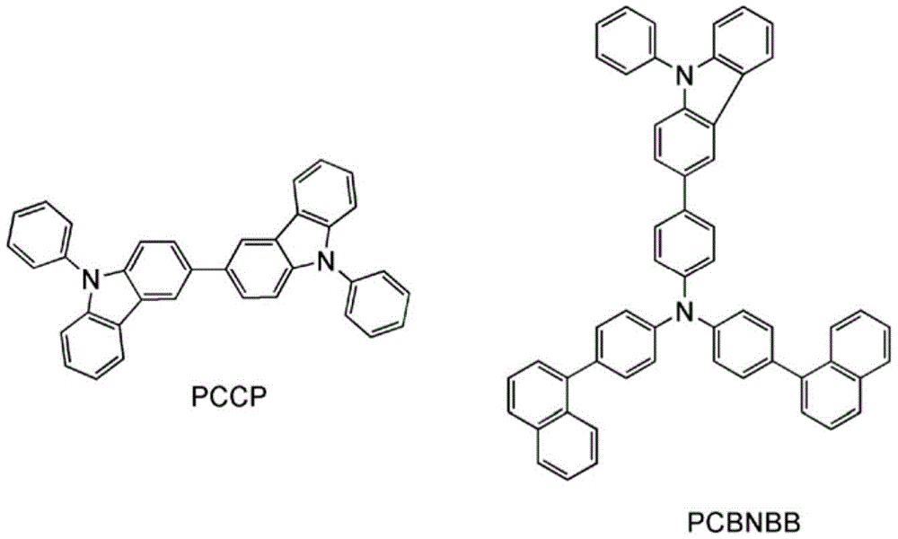
<吸收光谱><absorption spectrum>
图49A和图49B示出[Ir(mppr-Me)2(dpm)]的二氯甲烷溶液中 [Ir(mppr-Me)2(dpm)]的紫外可见吸收光谱(吸收光谱f)。在吸收光谱的测量中,使用紫外可见分光光度计(日本分光株式会社(JASCO Corporation)制造的V550型),将二氯甲烷溶液(0.093mmol/L)放在石英皿中,并在室温下进行测量。49A and 49B show the UV-Vis absorption spectrum (absorption spectrum f) of [Ir(mppr-Me) 2 (dpm)] in a dichloromethane solution of [Ir(mppr-Me) 2 (dpm)]. In the measurement of the absorption spectrum, using an ultraviolet-visible spectrophotometer (Model V550 manufactured by JASCO Corporation), a dichloromethane solution (0.093 mmol/L) was placed in a quartz dish, and the measurement was carried out at room temperature. Measurement.
<发射光谱><Emission spectrum>
图49A和图49B还示出2mDBTPDBq-II和PCBNBB的混合材料的薄膜的发射光谱(发射光谱f-1)、2mDBTPDBq-II和PCCP的混合材料的薄膜的发射光谱(发射光谱f-2)。在图49A中,横轴表示波长(nm),而纵轴表示摩尔吸光系数ε(M-1·cm-1)及发光强度(任意单位)。在图49B中,横轴表示能量(eV),而纵轴表示摩尔吸光系数ε(M-1·cm-1) 及发光强度(任意单位)。49A and 49B also show the emission spectrum of the thin film of the mixed material of 2mDBTPDBq-II and PCBNBB (emission spectrum f-1), the emission spectrum of the thin film of the mixed material of 2mDBTPDBq-II and PCCP (emission spectrum f-2). In FIG. 49A , the horizontal axis represents wavelength (nm), and the vertical axis represents molar absorption coefficient ε (M -1 ·cm -1 ) and luminous intensity (arbitrary unit). In FIG. 49B , the horizontal axis represents energy (eV), and the vertical axis represents molar absorption coefficient ε (M −1 ·cm −1 ) and luminous intensity (arbitrary unit).
从图49A的吸收光谱f可知,[Ir(mppr-Me)2(dpm)]在500nm附近具有宽吸收带。可以认为该吸收带对发光贡献很大。From the absorption spectrum f of FIG. 49A , [Ir(mppr-Me) 2 (dpm)] has a broad absorption band around 500 nm. It is considered that this absorption band greatly contributes to light emission.
发射光谱f-1及发射光谱f-2的峰值与吸收光谱f中的可认为是对发光贡献很大的吸收带的重叠很大。从而,可知由于利用主体材料的发射光谱与客体材料的吸收光谱的重叠进行能量转移,将本实施例的客体材料及主体材料都用于发光层的发光元件具有高能量转移效率。因此,可知可以得到外部量子效率高的发光元件。The peaks of the emission spectrum f-1 and the emission spectrum f-2 have a large overlap with the absorption band in the absorption spectrum f that is considered to greatly contribute to light emission. Therefore, it can be seen that the light-emitting element using both the guest material and the host material of the present embodiment for the light-emitting layer has high energy transfer efficiency due to the superposition of the emission spectrum of the host material and the absorption spectrum of the guest material for energy transfer. Therefore, it was found that a light-emitting element having a high external quantum efficiency can be obtained.
此外,从实施例14可知,可以使用含咔唑化合物的混合材料或含芳香胺化合物的混合材料作为主体材料。In addition, as can be seen from Example 14, a carbazole compound-containing mixed material or an aromatic amine compound-containing mixed material can be used as the host material.
实施例15Example 15
在本实施例15中,参照图2说明本发明的一个方式的发光元件。由于在本实施例中使用的材料是在上述实施例中使用的材料,所以在此省略化学式。In the fifteenth embodiment, a light-emitting element according to one embodiment of the present invention will be described with reference to FIG. 2 . Since the materials used in this embodiment are those used in the above-described embodiments, chemical formulae are omitted here.
以下示出本实施例的发光元件13及14的制造方法。The manufacturing method of the light-emitting elements 13 and 14 of this Example is shown below.
(发光元件13)(Light-emitting element 13)
首先,在玻璃衬底1100上通过溅射法形成ITSO膜,由此形成用作阳极的第一电极1101。将其厚度设定为110nm,且将其电极面积设定为2mm×2mm。First, an ITSO film is formed on a
接着,作为在衬底1100上形成发光元件的预处理,用水洗涤衬底表面,在200℃下进行焙烧1小时,进行UV臭氧处理370秒。Next, as a pretreatment for forming a light-emitting element on the
然后,在将衬底1100放入到其内部被减压到10-4Pa左右的真空蒸镀装置中,并在真空蒸镀装置的加热室中以170℃进行30分钟的真空焙烧,然后对衬底1100进行30分钟左右的冷却。Then, the
接着,以使其上形成有第一电极1101的表面面朝下的方式将形成有第一电极1101的衬底1100固定在真空蒸镀装置内的衬底支架上。将真空蒸镀装置内的压力减压到10-4Pa左右。然后,在第一电极1101 上共蒸镀BPAFLP和氧化钼(Ⅵ),以形成空穴注入层1111。将空穴注入层1111的厚度设定为40nm,将BPAFLP与氧化钼的重量比调节为 4:2(=BPAFLP:氧化钼)。Next, the
接着,在空穴注入层1111上形成厚度为20nm的BPAFLP膜,来形成空穴传输层1112。Next, a BPAFLP film with a thickness of 20 nm was formed on the
再者,共蒸镀2mDBTPDBq-II、PCBNBB和[Ir(mppr-Me)2(dpm)],以在空穴传输层1112上形成发光层1113。在此,将2mDBTPDBq-II、 PCBNBB、[Ir(mppr-Me)2(dpm)]的重量比调节为 0.8:0.2:0.05(=2mDBTPDBq-II:PCBNBB:[Ir(mppr-Me)2(dpm)])。将发光层1113的厚度设定为20nm。Furthermore, 2mDBTPDBq-II, PCBNBB and [Ir(mppr-Me) 2 (dpm)] were co-evaporated to form a
接着,在发光层1113上共蒸镀2mDBTPDBq-II、PCBNBB及 [Ir(mppr-Me)2(dpm)],以在发光层1113上形成第一电子传输层1114a。将2mDBTPDBq-II、PCBNBB、[Ir(mppr-Me)2(dpm)]的重量比调节为 0.8:0.2:0.05(=2mDBTPDBq-II:PCBNBB:[Ir(mppr-Me)2(dpm)])。将第一电子传输层1114a的厚度设定为40nm。Next, 2mDBTPDBq-II, PCBNBB and [Ir(mppr-Me) 2 (dpm)] were co-evaporated on the light-emitting
接着,在第一电子传输层1114a上形成厚度为10nm的BPhen膜,来形成第二电子传输层1114b。Next, a BPhen film having a thickness of 10 nm was formed on the first
然后,在第二电子传输层1114b上通过蒸镀形成厚度为1nm的LiF 膜,来形成电子注入层1115。Then, an electron injection layer 1115 was formed by forming a LiF film with a thickness of 1 nm on the second
最后,通过蒸镀形成厚度为200nm的铝膜,以形成用作阴极的第二电极1103。这样,制造本实施例的发光元件13。Finally, an aluminum film with a thickness of 200 nm was formed by vapor deposition to form a
(发光元件14)(Light-emitting element 14)
通过共蒸发2mDBTPDBq-II、9-苯基-9H-3-(9-苯基-9H-咔唑-3-基) 咔唑(缩写:PCCP)、[Ir(mppr-Me)2(dpm)]来形成发光元件14的发光层 1113。将2mDBTPDBq-II、PCCP、[Ir(mppr-Me)2(dpm)]的重量比调节为 0.8:0.2:0.05(=2mDBTPDBq-II:PCCP:[Ir(mppr-Me)2(dpm)])。将发光层1113的厚度设定为20nm。除了发光层1113之外的层通过采用与发光元件13同样的方式制造。By co-evaporation of 2mDBTPDBq-II, 9-phenyl-9H-3-(9-phenyl-9H-carbazol-3-yl)carbazole (abbreviation: PCCP), [Ir(mppr-Me) 2 (dpm) ] to form the light-emitting
注意,在上述蒸镀过程中,均采用电阻加热法进行蒸镀。Note that, in the above evaporation process, the resistance heating method was used for evaporation.
表15示出通过上述步骤获得的发光元件13及14的元件结构。Table 15 shows the element structures of the light-emitting elements 13 and 14 obtained by the above steps.
[表15][Table 15]
在含有氮气氛的手套箱中,以不暴露于空气的方式对这些发光元件进行密封。然后,对这些发光元件的工作特性进行测量。注意,在室温下(在保持于25℃的气氛中)进行测量。These light-emitting elements were sealed in a glove box containing a nitrogen atmosphere so as not to be exposed to air. Then, the operation characteristics of these light-emitting elements were measured. Note that the measurement was performed at room temperature (in an atmosphere maintained at 25°C).
图50示出发光元件13及14的电流密度-亮度特性。在图50中,横轴表示电流密度(mA/cm2),而纵轴表示亮度(cd/m2)。图51示出电压-亮度特性。在图51中,横轴表示电压(V),而纵轴表示亮度(cd/m2)。图52示出亮度-电流效率特性。在图52中,横轴表示亮度(cd/m2),而纵轴表示电流效率(cd/A)。图53示出亮度-外部量子效率特性。在图53中,横轴表示亮度(cd/m2),而纵轴表示外部量子效率(%)。FIG. 50 shows the current density-luminance characteristics of the light-emitting elements 13 and 14. In FIG. 50 , the horizontal axis represents current density (mA/cm 2 ), and the vertical axis represents luminance (cd/m 2 ). FIG. 51 shows the voltage-luminance characteristics. In FIG. 51 , the horizontal axis represents voltage (V), and the vertical axis represents luminance (cd/m 2 ). FIG. 52 shows luminance-current efficiency characteristics. In FIG. 52 , the horizontal axis represents luminance (cd/m 2 ), and the vertical axis represents current efficiency (cd/A). FIG. 53 shows luminance-external quantum efficiency characteristics. In FIG. 53 , the horizontal axis represents luminance (cd/m 2 ), and the vertical axis represents external quantum efficiency (%).
此外,表16示出发光元件13及14在亮度大约1200cd/m2时的电压(V)、电流密度(mA/cm2)、CIE色坐标(x,y)、电流效率(cd/A)、功率效率(lm/W)和外部量子效率(%)。In addition, Table 16 shows the voltage (V), current density (mA/cm 2 ), CIE color coordinates (x, y), and current efficiency (cd/A) of the light-emitting elements 13 and 14 at a luminance of about 1200 cd/m 2 , power efficiency (lm/W) and external quantum efficiency (%).
[表16][Table 16]
图54示出施加0.1mA的电流而得到的发光元件13及14的发射光谱。在图54中,横轴表示波长(nm),而纵轴表示发光强度(任意单位)。如表16所示那样,1200cd/m2的亮度下的发光元件13的CIE色坐标为(x,y)=(0.54,0.45),1200cd/m2的亮度下的发光元件14的CIE色坐标为(x,y)=(0.54,0.46)。从上述结果可知,发光元件13和14 发射来源于[Ir(mppr-Me)2(dpm)]的橙色光。FIG. 54 shows the emission spectra of the light-emitting elements 13 and 14 obtained by applying a current of 0.1 mA. In FIG. 54, the horizontal axis represents wavelength (nm), and the vertical axis represents luminous intensity (arbitrary unit). As shown in Table 16, the CIE color coordinates of the light-emitting element 13 at a luminance of 1200 cd/m 2 are (x, y)=(0.54, 0.45), and the CIE color coordinates of the light-emitting element 14 at a luminance of 1200 cd/m 2 is (x, y)=(0.54, 0.46). As can be seen from the above results, the light-emitting elements 13 and 14 emit orange light derived from [Ir(mppr-Me) 2 (dpm)].
从表16及图50至图53可知,发光元件13及14均具有高电流效率、高功率效率和高外部量子效率。As can be seen from Table 16 and FIGS. 50 to 53 , the light-emitting elements 13 and 14 have high current efficiency, high power efficiency, and high external quantum efficiency.
发光元件13的发光层包含实施例14所示的2mDBTPDBq-II、PCBNBB 及[Ir(mppr-Me)2(dpm)],发光元件14的发光层包含实施例14所示的 2mDBTPDBq-II、PCCP及[Ir(mppr-Me)2(dpm)]。如实施例14所述, 2mDBTPDBq-II和PCBNBB的混合材料以及2mDBTPDBq-II和PCCP的混合材料的发射光谱与[Ir(mppr-Me)2(dpm)]的吸收光谱中的可认为对发光贡献很大的吸收带的重叠大。由于利用该重叠进行能量转移,所以发光元件13及14可以认为具有高能量转移效率及高外部量子效率。The light-emitting layer of the light-emitting element 13 includes 2mDBTPDBq-II, PCBNBB and [Ir(mppr-Me) 2 (dpm)] shown in Example 14, and the light-emitting layer of the light-emitting element 14 includes 2mDBTPDBq-II, PCCP shown in Example 14 and [Ir(mppr-Me) 2 (dpm)]. As described in Example 14, the emission spectra of the mixed material of 2mDBTPDBq-II and PCBNBB and the mixed material of 2mDBTPDBq-II and PCCP and the absorption spectrum of [Ir(mppr-Me) 2 (dpm)] can be considered to contribute to luminescence The overlap of the very large absorption bands is large. The light-emitting elements 13 and 14 can be considered to have high energy transfer efficiency and high external quantum efficiency due to energy transfer using this overlap.
此外,从实施例15可知,在作为发光层的主体材料使用含咔唑化合物(PCCP)的混合材料而代替含芳香胺化合物(PCBNBB)的混合材料时,也可以得到外部量子效率高的发光元件。In addition, as shown in Example 15, when a mixed material containing a carbazole compound (PCCP) is used as the host material of the light-emitting layer instead of a mixed material containing an aromatic amine compound (PCBNBB), a light-emitting element with high external quantum efficiency can be obtained. .
从上述结果可知,通过应用本发明的一个方式,可以实现外部量子效率高的发光元件。From the above results, it was found that a light-emitting element having a high external quantum efficiency can be realized by applying one aspect of the present invention.
(参考例1)(Reference Example 1)
以下,示出在上述实施例中使用的有机金属配合物,即(乙酰丙酮根)双(4,6-二苯基嘧啶根)铱(III)(别称:双[2-(6-苯基-4-嘧啶基-κN3)苯基-κC](2,4-戊二酮-κ2O,O’)铱(III))(缩写: [Ir(dppm)2(acac)])的合成例。以下,示出[Ir(dppm)2(acac)]的结构。Hereinafter, the organometallic complex used in the above-mentioned Examples, namely (acetylacetonate)bis(4,6-diphenylpyrimidinato)iridium(III) (another name: bis[2-(6-phenyl) Synthesis of -4-pyrimidinyl-κN3)phenyl-κC](2,4-pentanedione- κ2O ,O')iridium(III)) (abbreviation: [Ir(dppm) 2 (acac)]) example. The structure of [Ir(dppm) 2 (acac)] is shown below.

<步骤1:4,6-二苯基嘧啶(缩写:Hdppm)的合成><Step 1: Synthesis of 4,6-diphenylpyrimidine (abbreviation: Hdppm)>
首先,在装有回流管的回收烧瓶中放入5.02g 4,6-二氯嘧啶、 8.29g苯基硼酸、7.19g碳酸钠、0.29g双(三苯基膦)合钯(II)二氯化物(缩写:Pd(PPh3)2Cl2)、20mL水和20mL乙腈,且将烧瓶中的空气替换为氩气。通过对该反应容器照射微波(2.45GHz,100W)60分钟来进行加热。在此,在烧瓶中进一步放入2.08g苯基硼酸、1.79g碳酸钠、 0.070g Pd(PPh3)2Cl2、5mL水和5mL乙腈,且通过对混合物再次使用微波(2.45GHz,100W)照射60分钟进行加热。然后,将水加到该溶液中且将有机层用二氯甲烷萃取。将所得到的萃取液用水洗涤且用硫酸镁干燥。在干燥之后,将溶液过滤。将该溶液的溶剂蒸馏出,且随后使用二氯甲烷作为展开溶剂通过硅胶柱色谱法对所得到的残余物进行纯化,其结果,得到嘧啶衍生物Hdppm(黄白色粉末,产率38%)。注意,对于微波照射,使用微波合成装置(由CEM公司(CEMCorporation)制造,Discover)。步骤1的合成方案(a-1)显示如下。First, 5.02 g of 4,6-dichloropyrimidine, 8.29 g of phenylboronic acid, 7.19 g of sodium carbonate, and 0.29 g of bis(triphenylphosphine)palladium(II) dichloride were placed in a recovery flask equipped with a reflux tube. compound (abbreviation: Pd(PPh 3 ) 2 Cl 2 ), 20 mL of water and 20 mL of acetonitrile, and the air in the flask was replaced with argon. Heating was performed by irradiating the reaction vessel with microwaves (2.45 GHz, 100 W) for 60 minutes. Here, 2.08 g of phenylboronic acid, 1.79 g of sodium carbonate, 0.070 g of Pd(PPh 3 ) 2 Cl 2 , 5 mL of water and 5 mL of acetonitrile were further placed in the flask, and the mixture was again subjected to microwave (2.45 GHz, 100 W) Heating by irradiation for 60 minutes. Then, water was added to the solution and the organic layer was extracted with dichloromethane. The resulting extract was washed with water and dried over magnesium sulfate. After drying, the solution was filtered. The solvent of the solution was distilled off, and then the obtained residue was purified by silica gel column chromatography using dichloromethane as a developing solvent, as a result, a pyrimidine derivative Hdppm was obtained (yellow-white powder, yield 38%). Note that, for microwave irradiation, a microwave synthesis apparatus (manufactured by CEM Corporation, Discover) was used. The synthetic scheme (a-1) of

<步骤2:二-μ-氯-双[双(4,6-二苯基嘧啶根)铱(III)](缩写: [Ir(dppm)2Cl]2)的合成><Step 2: Synthesis of bis-μ-chloro-bis[bis(4,6-diphenylpyrimidinyl)iridium(III)] (abbreviation: [Ir(dppm) 2 Cl] 2 )>
接着,在装有回流管的回收烧瓶中放入15mL 2-乙氧基乙醇、5mL 水、1.10g在上述步骤1中得到的Hdppm和0.69g氯化铱水合物 (IrCl3·H2O),且将烧瓶中的空气替换为氩气。然后,进行微波(2.45GHz, 100W)照射1小时以引起反应。在将溶剂蒸馏出且将所得到的残余物用乙醇过滤并洗涤以得到双核配合物[Ir(dppm)2Cl]2(红棕色粉末,产率88%)。步骤2的合成方案(a-2)显示如下。Next, 15 mL of 2-ethoxyethanol, 5 mL of water, 1.10 g of Hdppm obtained in the

<步骤3:(乙酰丙酮根)双(4,6-二苯基嘧啶根)铱(III)(缩写: [Ir(dppm)2(acac)])的合成><Step 3: Synthesis of (acetylacetonate)bis(4,6-diphenylpyrimidine)iridium(III) (abbreviation: [Ir(dppm) 2 (acac)])>
再者,在装有回流管的回收烧瓶中放入40mL 2-乙氧基乙醇、1.44g 在上述步骤2中得到的[Ir(dppm)2Cl]2、0.30g乙酰丙酮和1.07g碳酸钠,且将烧瓶中的空气替换为氩气。然后,进行微波(2.45GHz,120W) 照射60分钟以引起反应。将溶剂蒸馏出,将得到的残余物溶解于二氯甲烷中,且进行过滤以除去不溶物质。将所得到的滤液用水洗涤且随后用饱和盐水洗涤,且用硫酸镁干燥。在干燥之后,将溶液过滤。将该溶液的溶剂蒸馏出,且随后通过硅胶柱色谱法使用体积比为50:1的二氯甲烷和乙酸乙酯作为展开溶剂对所得到的残余物进行纯化。然后,用二氯甲烷和己烷的混合溶剂进行重结晶,以得到作为目的物的橙色粉末(产率32%)。步骤3的合成方案(a-3)显示如下。Furthermore, 40 mL of 2-ethoxyethanol, 1.44 g of [Ir(dppm) 2 Cl] 2 obtained in the

在上述步骤3中得到的橙色粉末的核磁共振谱(1H NMR)的分析结果显示如下。从该结果可知得到了有机金属配合物[Ir(dppm)2(acac)]。The analysis results of the nuclear magnetic resonance spectrum ( 1 H NMR) of the orange powder obtained in the
1H NMR.δ(CDCl3):1.83(s,6H),5.29(s,1H),6.48(d,2H),6.80(t,2 H),6.90(t,2H),7.55-7.63(m,6H),7.77(d,2H),8.17(s,2H),8.24(d,4 H),9.17(s,2H). 1 H NMR. δ(CDCl 3 ): 1.83(s, 6H), 5.29(s, 1H), 6.48(d, 2H), 6.80(t, 2H), 6.90(t, 2H), 7.55-7.63( m, 6H), 7.77(d, 2H), 8.17(s, 2H), 8.24(d, 4H), 9.17(s, 2H).
(参考例2)(Reference example 2)
以下,示出在上述实施例中使用的有机金属配合物,即(乙酰丙酮根)双(6-甲基-4-苯基嘧啶根)铱(III)(别称:双[2-(6-甲基-4- 嘧啶基-κN3)苯基-κC](2,4-戊二酮根-κ2O,O’)铱(III))(缩写: [Ir(mppm)2(acac)])的合成例。以下,示出[Ir(mppm)2(acac)]的结构。Hereinafter, the organometallic complex used in the above-mentioned Examples, that is, (acetylacetonate)bis(6-methyl-4-phenylpyrimidinato)iridium(III) (another name: bis[2-(6- Methyl-4-pyrimidinyl-κN3)phenyl-κC](2,4-pentanedione- κ2O ,O')iridium(III)) (abbreviation: [Ir(mppm) 2 (acac)] ) synthesis example. The structure of [Ir(mppm) 2 (acac)] is shown below.

<步骤1:4-甲基-6-苯基嘧啶(缩写:Hmppm)的合成><Step 1: Synthesis of 4-methyl-6-phenylpyrimidine (abbreviation: Hmppm)>
首先,在装有回流管的回收烧瓶中放入4.90g 4-氯-6-甲基嘧啶、 4.80g苯基硼酸、4.03g碳酸钠、0.16g双(三苯基膦)合钯(II)二氯化物(缩写:Pd(PPh3)2Cl2)、20mL水和10mL乙腈,且将烧瓶中的空气替换为氩气。通过对该反应容器照射微波(2.45GHz,100W)60分钟来进行加热。在此,在烧瓶中进一步放入2.28g苯基硼酸、2.02g碳酸钠、 0.082g Pd(PPh3)2Cl2、5mL水和10mL乙腈,且通过对混合物再次使用微波(2.45GHz,100W)照射60分钟进行加热。然后,将水加到该溶液中且用二氯甲烷萃取。将所得到的萃取液用饱和碳酸钠水溶液、水洗涤且随后用饱和盐水洗涤,且用硫酸镁干燥。在干燥之后,将溶液过滤。将该溶液的溶剂蒸馏出,且随后通过硅胶柱色谱法使用体积比为9: 1的二氯甲烷和乙酸乙酯作为展开溶剂对所得到的残余物进行纯化,其结果,得到目的物嘧啶衍生物Hmppm(橙色油状物质,产率46%)。注意,对于微波照射,使用微波合成装置(由CEM公司(CEM Corporation) 制造,Discover)。步骤1的合成方案(b-1)显示如下。First, put 4.90g of 4-chloro-6-methylpyrimidine, 4.80g of phenylboronic acid, 4.03g of sodium carbonate, 0.16g of bis(triphenylphosphine)palladium(II) into a recovery flask equipped with a reflux tube Dichloride (abbreviation: Pd( PPh3 ) 2Cl2 ), 20 mL of water and 10 mL of acetonitrile, and the air in the flask was replaced with argon. Heating was performed by irradiating the reaction vessel with microwaves (2.45 GHz, 100 W) for 60 minutes. Here, 2.28 g of phenylboronic acid, 2.02 g of sodium carbonate, 0.082 g of Pd(PPh 3 ) 2 Cl 2 , 5 mL of water and 10 mL of acetonitrile were further placed in the flask, and the mixture was again subjected to microwave (2.45 GHz, 100 W) Heating by irradiation for 60 minutes. Then, water was added to the solution and extracted with dichloromethane. The resulting extract was washed with saturated aqueous sodium carbonate solution, water and then saturated brine, and dried over magnesium sulfate. After drying, the solution was filtered. The solvent of this solution was distilled off, and then the obtained residue was purified by silica gel column chromatography using dichloromethane and ethyl acetate in a volume ratio of 9:1 as a developing solvent, as a result, the objective pyrimidine derivative was obtained Hmppm (orange oily substance, yield 46%). Note that, for microwave irradiation, a microwave synthesis apparatus (manufactured by CEM Corporation, Discover) was used. The synthetic scheme (b-1) of

<步骤2:二-μ-氯-双[双(6-甲基-4-苯基嘧啶根)铱(III)](缩写: [Ir(mppm)2Cl]2)的合成><Step 2: Synthesis of bis-μ-chloro-bis[bis(6-methyl-4-phenylpyrimidinato)iridium(III)] (abbreviation: [Ir(mppm) 2 Cl] 2 )>
接着,在装有回流管的回收烧瓶中放入15mL 2-乙氧基乙醇、5mL 水、1.51g在上述步骤1中得到的Hmppm和1.26g氯化铱水合物 (IrCl3·H2O),且将烧瓶中的空气替换为氩气。然后,进行微波(2.45GHz, 100W)照射1小时以引起反应。将溶剂蒸馏出,再将所得到的残余物用乙醇洗涤并过滤以得到双核配合物[Ir(mppm)2Cl]2(深绿色粉末,产率77%)。步骤2的合成方案(b-2)显示如下。Next, 15 mL of 2-ethoxyethanol, 5 mL of water, 1.51 g of Hmppm obtained in the

<步骤3:(乙酰丙酮根)双(6-甲基-4-苯基嘧啶根)铱(III)(缩写: [Ir(mppm)2(acac)])的合成><Step 3: Synthesis of (acetylacetonate)bis(6-methyl-4-phenylpyrimidine)iridium(III) (abbreviation: [Ir(mppm) 2 (acac)])>
再者,在装有回流管的回收烧瓶中放入40mL 2-乙氧基乙醇、1.84g 在上述步骤2中得到的双核配合物[Ir(mppm)2Cl]2、0.48g乙酰丙酮和1.73g碳酸钠,且将烧瓶中的空气替换为氩气。然后,进行微波 (2.45GHz,120W)照射60分钟以引起反应。将溶剂蒸馏出,将得到的残余物溶解于二氯甲烷中,且进行过滤以除去不溶物质。将所得到的滤液用水洗涤且随后用饱和盐水洗涤,且用硫酸镁干燥。在干燥之后,将溶液过滤。将该溶液的溶剂蒸馏出,且随后通过硅胶柱色谱法使用体积比为4:1的二氯甲烷和乙酸乙酯作为展开溶剂对所得到的残余物进行纯化。然后,用二氯甲烷和己烷的混合溶剂进行重结晶以得到作为目的物的黄色粉末(产率22%)。步骤3的合成方案(b-3)显示如下。Furthermore, 40 mL of 2-ethoxyethanol, 1.84 g of the binuclear complex [Ir(mppm) 2 Cl] 2 obtained in the

在上述步骤3中得到的黄色粉末的核磁共振谱(1H NMR)的分析结果显示如下。从该结果可知得到了有机金属配合物[Ir(mppm)2(acac)]。The analysis results of the nuclear magnetic resonance spectrum ( 1 H NMR) of the yellow powder obtained in the
1H NMR.δ(CDCl3):1.78(s,6H),2.81(s,6H),5.24(s,1H),6.37(d,2 H),6.77(t,2H),6.85(t,2H),7.61-7.63(m,4H),8.97(s,2H). 1 H NMR. δ(CDCl 3 ): 1.78(s, 6H), 2.81(s, 6H), 5.24(s, 1H), 6.37(d, 2H), 6.77(t, 2H), 6.85(t, 2H), 7.61-7.63(m, 4H), 8.97(s, 2H).
(参考例3)(Reference Example 3)
以下,示出在上述实施例中使用的有机金属配合物,即(乙酰丙酮根)双(6-叔丁基-4-苯基嘧啶根)铱(III)(别称:双[2-(6-叔丁基-4-嘧啶基-κN3)苯基-κC](2,4-戊二酮根-κ2O,O’)铱(III))(缩写:[Ir(tBuppm)2(acac)])的合成例。以下,示出[Ir(tBuppm)2(acac)] 的结构。Hereinafter, the organometallic complex used in the above-mentioned Examples, namely (acetylacetonate)bis(6-tert-butyl-4-phenylpyrimidinato)iridium(III) (another name: bis[2-(6), is shown below. -tert-Butyl-4-pyrimidinyl-κN3)phenyl-κC](2,4-pentanedione- κ2O ,O')iridium(III)) (abbreviation: [Ir(tBuppm) 2 (acac )]) synthesis example. The structure of [Ir(tBuppm) 2 (acac)] is shown below.
<步骤1:4-叔丁基-6-苯基嘧啶(缩写:HtBuppm)的合成><Step 1: Synthesis of 4-tert-butyl-6-phenylpyrimidine (abbreviation: HtBuppm)>
首先,在装有回流管的回收烧瓶中放入22.5g 4,4-二甲基-1-苯基戊烷-1,3-二酮和50g甲酰胺,且将烧瓶中的空气替换为氮气。加热该反应容器以将反应溶液回流5小时。然后,将该溶液注入氢氧化钠水溶液,将有机层用二氯甲烷萃取。将所得到的有机层用水、饱和盐水洗涤且用硫酸镁干燥。在干燥之后,将溶液过滤。将该溶液的溶剂蒸馏出,且随后通过硅胶柱色谱法使用体积比为10:1的己烷和乙酸乙酯作为展开溶剂对所得到的残余物进行纯化,其结果,得到嘧啶衍生物 HtBuppm(无色油状物质,产率14%)。步骤1的合成方案(c-1)显示如下。First, 22.5 g of 4,4-dimethyl-1-phenylpentane-1,3-dione and 50 g of formamide were placed in a recovery flask equipped with a reflux tube, and the air in the flask was replaced with nitrogen gas . The reaction vessel was heated to reflux the reaction solution for 5 hours. Then, this solution was poured into an aqueous sodium hydroxide solution, and the organic layer was extracted with dichloromethane. The obtained organic layer was washed with water, saturated brine and dried over magnesium sulfate. After drying, the solution was filtered. The solvent of this solution was distilled off, and then the obtained residue was purified by silica gel column chromatography using hexane and ethyl acetate in a volume ratio of 10:1 as a developing solvent, as a result, a pyrimidine derivative HtBuppm ( Colorless oily substance, 14% yield). The synthetic scheme (c-1) of

<步骤2:二-μ-氯-双[双(6-叔丁基-4-苯基嘧啶根)铱(III)](缩写:[Ir(tBuppm)2Cl]2)的合成><Step 2: Synthesis of bis-μ-chloro-bis[bis(6-tert-butyl-4-phenylpyrimidinato)iridium(III)] (abbreviation: [Ir(tBuppm) 2 Cl] 2 )>
接着,在装有回流管的回收烧瓶中放入15mL 2-乙氧基乙醇、5mL 水、1.49g在上述步骤1中得到的HtBuppm和1.04g氯化铱水合物 (IrCl3·H2O),且将烧瓶中的空气替换为氩气。然后,进行微波(2.45GHz, 100W)照射1小时以引起反应。将溶剂蒸馏出,且随后将所得到的残余物用乙醇抽滤并洗涤以得到双核配合物[Ir(tBuppm)2Cl]2(黄绿色粉末,产率73%)。步骤2的合成方案(c-2)显示如下。Next, 15 mL of 2-ethoxyethanol, 5 mL of water, 1.49 g of HtBuppm obtained in the

<步骤3:(乙酰丙酮根)双(6-叔丁基-4-苯基嘧啶根)铱(III)(缩写:[Ir(tBuppm)2(acac)])的合成><Step 3: Synthesis of (acetylacetonate)bis(6-tert-butyl-4-phenylpyrimidinato)iridium(III) (abbreviation: [Ir(tBuppm) 2 (acac)])>
再者,在装有回流管的回收烧瓶中放入40mL 2-乙氧基乙醇、1.61g 在上述步骤2中得到的双核配合物[Ir(tBuppm)2Cl]2、0.36g乙酰丙酮和1.27g碳酸钠,且将烧瓶中的空气替换为氩气。然后,进行微波 (2.45GHz,120W)照射60分钟以引起反应。将溶剂蒸馏出,将得到的残余物用乙醇抽滤并用水、乙醇洗涤。将该固体溶解于二氯甲烷中,将混合物通过以硅藻土(Celite)(日本和光纯药工业株式会社(Wako Pure Chemical Industries,Ltd.)生产、目录号码:531-16855)、氧化铝、硅藻土的顺序层叠的过滤助剂进行过滤。将溶剂蒸馏出,用二氯甲烷和己烷的混合溶剂对得到的固体进行重结晶,得到作为目的物的黄色粉末(产率68%)。步骤3的合成方案(c-3)显示如下。Furthermore, 40 mL of 2-ethoxyethanol, 1.61 g of the binuclear complex [Ir(tBuppm) 2 Cl] 2 obtained in the
在上述步骤3中得到的黄色粉末的核磁共振谱(1H NMR)的分析结果显示如下。从该结果可知得到了有机金属配合物[Ir(tBuppm)2(acac)]。The analysis results of the nuclear magnetic resonance spectrum ( 1 H NMR) of the yellow powder obtained in the
1H NMR.δ(CDCl3):1.50(s,18H),1.79(s,6H),5.26(s,1H),6.33(d, 2H),6.77(t,2H),6.85(t,2H),7.70(d,2H),7.76(s,2H),9.02(s,2H). 1 H NMR. δ(CDCl 3 ): 1.50(s, 18H), 1.79(s, 6H), 5.26(s, 1H), 6.33(d, 2H), 6.77(t, 2H), 6.85(t, 2H) ), 7.70(d, 2H), 7.76(s, 2H), 9.02(s, 2H).
(参考例4)(Reference Example 4)
以下说明在上述实施例中使用的2-[3-(二苯并噻吩-4-基)苯基] 二苯并[f,h]喹喔啉(缩写:2mDBTPDBq-II)的合成方法。The method for synthesizing 2-[3-(dibenzothiophen-4-yl)phenyl]dibenzo[f,h]quinoxaline (abbreviation: 2mDBTPDBq-II) used in the above-mentioned Examples is described below.

<2-[3-(二苯并噻吩-4-基)苯基]二苯并[f,h]喹喔啉(缩写: 2mDBTPDBq-II)的合成><Synthesis of 2-[3-(dibenzothiophen-4-yl)phenyl]dibenzo[f,h]quinoxaline (abbreviation: 2mDBTPDBq-II)>
2-[3-(二苯并噻吩-4-基)苯基]二苯并[f,h]喹喔啉(缩写: 2mDBTPDBq-II)的合成方案(d-1)显示如下。The synthetic scheme (d-1) of 2-[3-(dibenzothiophen-4-yl)phenyl]dibenzo[f,h]quinoxaline (abbreviation: 2mDBTPDBq-II) is shown below.

首先,在2L三颈烧瓶中放入5.3g(20mmol)2-氯二苯并[f,h]喹喔啉、6.1g(20mmol)3-(二苯并噻吩-4-基)苯基硼酸、460mg(0.4mmol) 四(三苯基膦)合钯(0)、300mL甲苯、20mL乙醇和20mL 2M碳酸钾水溶液。通过在减压下搅拌使该混合物脱气,且将三颈烧瓶中的空气替换为氮气。将该混合物在氮气流下在100℃下搅拌7.5小时。在冷却到室温之后,将得到的混合物过滤以得到白色物质。将得到的残余物用水和乙醇依次洗涤,随后干燥。将得到的固体溶解在大约600mL热甲苯中,接着通过硅藻土、硅酸镁(Florisil)抽滤,由此得到无色透明的滤液。将得到的滤液浓缩并通过使用大约700mL硅胶的柱色谱法纯化。该色谱法使用热甲苯作为展开溶剂进行。将丙酮和乙醇加到在此得到的固体中,接着用超声波照射。随后,将产生的悬浮固体过滤并将得到的固体干燥,以得到7.85g白色粉末,产率80%。First, put 5.3 g (20 mmol) of 2-chlorodibenzo[f,h]quinoxaline and 6.1 g (20 mmol) of 3-(dibenzothiophen-4-yl)phenylboronic acid into a 2L three-necked flask , 460 mg (0.4 mmol) of tetrakis(triphenylphosphine)palladium(0), 300 mL of toluene, 20 mL of ethanol, and 20 mL of 2M aqueous potassium carbonate solution. The mixture was degassed by stirring under reduced pressure, and the air in the three-necked flask was replaced with nitrogen. The mixture was stirred at 100°C for 7.5 hours under nitrogen flow. After cooling to room temperature, the resulting mixture was filtered to obtain a white material. The obtained residue was washed successively with water and ethanol, followed by drying. The obtained solid was dissolved in about 600 mL of hot toluene, followed by suction filtration through Celite and magnesium silicate (Florisil) to obtain a colorless and transparent filtrate. The resulting filtrate was concentrated and purified by column chromatography using approximately 700 mL of silica gel. The chromatography was carried out using hot toluene as developing solvent. Acetone and ethanol were added to the solid obtained here, followed by irradiation with ultrasonic waves. Subsequently, the resulting suspended solid was filtered and the resulting solid was dried to obtain 7.85 g of white powder with a yield of 80%.
上述目的物是相对可溶于热甲苯,但冷却时容易沉淀的材料。此外,该物质不易溶解于其他有机溶剂诸如丙酮和乙醇中。因此,利用这些不同程度的溶解度,可以通过上述简单方法高收率地合成。具体而言,在反应结束之后,将混合物回到室温,通过过滤来收集沉淀的固体,由此可以容易地去除大部分的杂质。此外,通过将热甲苯用作展开溶剂的柱色谱法,能够容易地纯化容易沉淀的目的物。The above-mentioned target substance is a material that is relatively soluble in hot toluene but tends to precipitate when cooled. Furthermore, the material is not readily soluble in other organic solvents such as acetone and ethanol. Therefore, taking advantage of these varying degrees of solubility, high-yield synthesis is possible by the simple method described above. Specifically, after the reaction was completed, the mixture was returned to room temperature, and the precipitated solid was collected by filtration, whereby most of the impurities could be easily removed. Further, by column chromatography in which hot toluene is used as a developing solvent, the object of interest, which is easily precipitated, can be easily purified.
通过梯度升华法纯化所得到的4.0g白色粉末。在压力为5.0Pa,且氩气流速为5毫升/分钟的条件下,以300℃加热白色粉末来进行纯化。纯化之后,得到3.5g作为目的物的白色粉末,产率88%。The resulting 4.0 g of white powder was purified by gradient sublimation. Purification was performed by heating the white powder at 300°C under a pressure of 5.0 Pa and an argon flow rate of 5 ml/min. After purification, 3.5 g of a white powder as the object was obtained with a yield of 88%.
使用核磁共振谱(1H NMR)确认该化合物为目的物2-[3-(二苯并噻吩-4-基)苯基]二苯并[f,h]喹喔啉(缩写:2mDBTPDBq-II)。This compound was confirmed to be the target 2-[3-(dibenzothiophen-4-yl)phenyl]dibenzo[f,h]quinoxaline (abbreviation: 2mDBTPDBq-II) using nuclear magnetic resonance spectroscopy ( 1 H NMR). ).
以下示出所得到的物质的1H NMR数据。The 1 H NMR data of the obtained substance are shown below.
1H NMR(CDCl3,300MHz):δ(ppm)=7.45-7.52(m,2H)、 7.59-7.65(m,2H)、7.71-7.91(m,7H)、8.20-8.25(m,2H)、 8.41(d,J=7.8Hz,1H)、8.65(d,J=7.5Hz,2H)、8.77-8.78(m,1H)、 9.23(dd,J=7.2Hz,1.5Hz,1H)、9.42(dd,J=7.8Hz,1.5Hz,1H)、 9.48(s,1H)。 1 H NMR (CDCl 3 , 300MHz): δ (ppm)=7.45-7.52 (m, 2H), 7.59-7.65 (m, 2H), 7.71-7.91 (m, 7H), 8.20-8.25 (m, 2H) , 8.41(d,J=7.8Hz,1H), 8.65(d,J=7.5Hz,2H), 8.77-8.78(m,1H), 9.23(dd,J=7.2Hz,1.5Hz,1H), 9.42 (dd, J=7.8 Hz, 1.5 Hz, 1H), 9.48 (s, 1H).
符号说明Symbol Description
102:EL层、103:第一电极、108:第二电极、701:空穴注入层、 702:空穴传输层、703:发光层、704:电子传输层、705:电子注入层、706:电子注入缓冲层、707:电子继电层、708:复合材料层、800:第一EL层、801:第二EL层、803:电荷发生层、1100:衬底、1101:第一电极、1103:第二电极、1111:空穴注入层、1112:空穴传输层、 1113:发光层、1114a:第一电子传输层、1114b:第二电子传输层、 1115:电子注入层102: EL layer, 103: first electrode, 108: second electrode, 701: hole injection layer, 702: hole transport layer, 703: light emitting layer, 704: electron transport layer, 705: electron injection layer, 706: Electron injection buffer layer, 707: electron relay layer, 708: composite material layer, 800: first EL layer, 801: second EL layer, 803: charge generating layer, 1100: substrate, 1101: first electrode, 1103 : second electrode, 1111: hole injection layer, 1112: hole transport layer, 1113: light emitting layer, 1114a: first electron transport layer, 1114b: second electron transport layer, 1115: electron injection layer
本申请基于2011年2月16日向日本专利局提交的日本专利申请第2011-031426号,其全部内容通过引用纳入本文。This application is based on Japanese Patent Application No. 2011-031426 filed with the Japan Patent Office on February 16, 2011, the entire contents of which are incorporated herein by reference.
Claims (61)
Applications Claiming Priority (3)
| Application Number | Priority Date | Filing Date | Title |
|---|---|---|---|
| JP2011031426 | 2011-02-16 | ||
| JP2011-031426 | 2011-02-16 | ||
| CN201280009003.0A CN103380509B (en) | 2011-02-16 | 2012-02-07 | Light emitting element |
Related Parent Applications (1)
| Application Number | Title | Priority Date | Filing Date |
|---|---|---|---|
| CN201280009003.0A Division CN103380509B (en) | 2011-02-16 | 2012-02-07 | Light emitting element |
Publications (2)
| Publication Number | Publication Date |
|---|---|
| CN106549112A CN106549112A (en) | 2017-03-29 |
| CN106549112B true CN106549112B (en) | 2020-01-07 |
Family
ID=46636354
Family Applications (2)
| Application Number | Title | Priority Date | Filing Date |
|---|---|---|---|
| CN201710017343.2A Active CN106549112B (en) | 2011-02-16 | 2012-02-07 | light-emitting element |
| CN201280009003.0A Active CN103380509B (en) | 2011-02-16 | 2012-02-07 | Light emitting element |
Family Applications After (1)
| Application Number | Title | Priority Date | Filing Date |
|---|---|---|---|
| CN201280009003.0A Active CN103380509B (en) | 2011-02-16 | 2012-02-07 | Light emitting element |
Country Status (7)
| Country | Link |
|---|---|
| US (7) | US8994263B2 (en) |
| JP (16) | JP5981726B2 (en) |
| KR (10) | KR102670436B1 (en) |
| CN (2) | CN106549112B (en) |
| DE (8) | DE112012007388B4 (en) |
| TW (8) | TWI738276B (en) |
| WO (1) | WO2012111580A1 (en) |
Families Citing this family (99)
| Publication number | Priority date | Publication date | Assignee | Title |
|---|---|---|---|---|
| EP2433929B1 (en) * | 2010-09-27 | 2013-10-23 | Semiconductor Energy Laboratory Co, Ltd. | Organic Compound, Light-Emitting Element, Light-Emitting Device, Electronic Device, and Lighting Device |
| DE202012013738U1 (en) | 2011-02-16 | 2020-11-05 | Semiconductor Energy Laboratory Co., Ltd. | Light emitting element |
| KR102670436B1 (en) | 2011-02-16 | 2024-05-28 | 가부시키가이샤 한도오따이 에네루기 켄큐쇼 | Light-emitting element |
| TWI563702B (en) | 2011-02-28 | 2016-12-21 | Semiconductor Energy Lab Co Ltd | Light-emitting device |
| US8969854B2 (en) | 2011-02-28 | 2015-03-03 | Semiconductor Energy Laboratory Co., Ltd. | Light-emitting layer and light-emitting element |
| KR20250018429A (en) | 2011-03-23 | 2025-02-05 | 가부시키가이샤 한도오따이 에네루기 켄큐쇼 | Light-emitting element |
| CN105702873B (en) | 2011-03-30 | 2017-11-24 | 株式会社半导体能源研究所 | Light-emitting component |
| KR102310048B1 (en) | 2011-04-07 | 2021-10-08 | 가부시키가이샤 한도오따이 에네루기 켄큐쇼 | Light-emitting element |
| KR102025266B1 (en) | 2011-04-29 | 2019-09-25 | 가부시키가이샤 한도오따이 에네루기 켄큐쇼 | Organometallic complex, light-emitting element, light-emitting device, electronic device, and lighting device |
| TWI532822B (en) | 2011-04-29 | 2016-05-11 | 半導體能源研究所股份有限公司 | Phosphorescent light emitting device, electronic device and lighting device |
| JP2013147490A (en) | 2011-12-23 | 2013-08-01 | Semiconductor Energy Lab Co Ltd | Iridium complex, light-emitting element, light-emitting device, electronic device, and lighting device |
| KR101803537B1 (en) | 2012-02-09 | 2017-11-30 | 가부시키가이샤 한도오따이 에네루기 켄큐쇼 | Light-emitting element |
| KR20200049908A (en) * | 2012-03-14 | 2020-05-08 | 가부시키가이샤 한도오따이 에네루기 켄큐쇼 | Light-emitting element, light-emitting device, electronic device, and lighting device |
| WO2013137089A1 (en) | 2012-03-14 | 2013-09-19 | Semiconductor Energy Laboratory Co., Ltd. | Light-emitting element, light-emitting device, display device, electronic device, and lighting device |
| JP2013232629A (en) | 2012-04-06 | 2013-11-14 | Semiconductor Energy Lab Co Ltd | Light-emitting element, light-emitting device, electronic device, and lighting device |
| JP6158543B2 (en) | 2012-04-13 | 2017-07-05 | 株式会社半導体エネルギー研究所 | LIGHT EMITTING ELEMENT, LIGHT EMITTING DEVICE, ELECTRONIC DEVICE, AND LIGHTING DEVICE |
| JP6158542B2 (en) | 2012-04-13 | 2017-07-05 | 株式会社半導体エネルギー研究所 | LIGHT EMITTING ELEMENT, LIGHT EMITTING DEVICE, ELECTRONIC DEVICE, AND LIGHTING DEVICE |
| DE112013002110B4 (en) | 2012-04-20 | 2017-09-07 | Semiconductor Energy Laboratory Co., Ltd. | Light emitting element, light emitting device, electronic device and lighting device |
| JP6076153B2 (en) | 2012-04-20 | 2017-02-08 | 株式会社半導体エネルギー研究所 | LIGHT EMITTING ELEMENT, LIGHT EMITTING DEVICE, DISPLAY DEVICE, ELECTRONIC DEVICE, AND LIGHTING DEVICE |
| KR20240129241A (en) | 2012-04-20 | 2024-08-27 | 가부시키가이샤 한도오따이 에네루기 켄큐쇼 | Light-emitting element, light-emitting device, electronic appliance, and lighting device |
| US8994013B2 (en) | 2012-05-18 | 2015-03-31 | Semiconductor Energy Laboratory Co., Ltd. | Light-emitting element, light-emitting device, display device, electronic device, and lighting device |
| US8916897B2 (en) | 2012-05-31 | 2014-12-23 | Semiconductor Energy Laboratory Co., Ltd. | Light-emitting element, light-emitting device, display device, electronic device, and lighting device |
| DE102013208844A1 (en) | 2012-06-01 | 2013-12-05 | Semiconductor Energy Laboratory Co., Ltd. | Light emitting element, light emitting device, display device, electronic device and lighting device |
| US8921549B2 (en) | 2012-06-01 | 2014-12-30 | Semiconductor Energy Laboratory Co., Ltd. | Organometallic complex, light-emitting element, light-emitting device, electronic device, and lighting device |
| US20140014930A1 (en) | 2012-07-13 | 2014-01-16 | Semiconductor Energy Laboratory Co., Ltd. | Organic Compound, Light-Emitting Element, Light-Emitting Device, Electronic Device, and Lighting Device |
| KR102438674B1 (en) | 2012-08-03 | 2022-08-31 | 가부시키가이샤 한도오따이 에네루기 켄큐쇼 | Light-emitting element, light-emitting device, display device, electronic appliance, and lighting device |
| JP2014043437A (en) | 2012-08-03 | 2014-03-13 | Semiconductor Energy Lab Co Ltd | Organic compound, light-emitting element, light-emitting device, electronic device, and lighting device |
| CN104508850B (en) | 2012-08-03 | 2017-03-22 | 株式会社半导体能源研究所 | Light-emitting element, light-emitting device, electronic device, and lighting device |
| TWI679790B (en) | 2012-08-03 | 2019-12-11 | 日商半導體能源研究所股份有限公司 | Light-emitting element |
| TWI651878B (en) | 2012-08-03 | 2019-02-21 | 日商半導體能源研究所股份有限公司 | Light-emitting element, light-emitting device, display device, electronic device and lighting device |
| US9142710B2 (en) | 2012-08-10 | 2015-09-22 | Semiconductor Energy Laboratory Co., Ltd. | Light-emitting element, light-emitting device, display device, electronic device, and lighting device |
| WO2014054551A1 (en) * | 2012-10-03 | 2014-04-10 | Semiconductor Energy Laboratory Co., Ltd. | Light-emitting device, electronic device, and lighting device |
| US9203045B2 (en) | 2012-11-29 | 2015-12-01 | Semiconductor Energy Laboratory Co., Ltd. | Light-emitting element, light-emitting device, electronic device, and lighting device |
| KR102151394B1 (en) | 2013-01-10 | 2020-09-04 | 가부시키가이샤 한도오따이 에네루기 켄큐쇼 | Light-emitting element, light-emitting device, electronic device, and lighting device |
| JP6047416B2 (en) * | 2013-02-18 | 2016-12-21 | 日本放送協会 | Evaluation method of organic electroluminescence device |
| US10043982B2 (en) | 2013-04-26 | 2018-08-07 | Semiconductor Energy Laboratory Co., Ltd. | Light-emitting element, light-emitting device, display device, electronic device, and lighting device |
| KR102763019B1 (en) | 2013-05-16 | 2025-02-07 | 가부시키가이샤 한도오따이 에네루기 켄큐쇼 | Light-emitting element, light-emitting device, electronic device, and lighting device |
| KR102214317B1 (en) | 2013-06-14 | 2021-02-08 | 가부시키가이샤 한도오따이 에네루기 켄큐쇼 | Organometallic iridium complex, light-emitting element, light-emitting device, and lighting device |
| US9130182B2 (en) | 2013-06-28 | 2015-09-08 | Semiconductor Energy Laboratory Co., Ltd. | Light-emitting element, lighting device, light-emitting device, and electronic device |
| KR102022533B1 (en) | 2013-08-26 | 2019-09-19 | 가부시키가이샤 한도오따이 에네루기 켄큐쇼 | Light-emitting device |
| DE112014005483B4 (en) | 2013-12-02 | 2022-01-20 | Semiconductor Energy Laboratory Co., Ltd. | Light-emitting element, display module, lighting module, light-emitting device, display device, electronic device and lighting device |
| KR102088883B1 (en) * | 2013-12-02 | 2020-03-16 | 엘지디스플레이 주식회사 | Organic Light Emitting Display Device |
| CN105981191B (en) | 2013-12-02 | 2019-01-22 | 株式会社半导体能源研究所 | Light-emitting element, light-emitting device, electronic equipment, and lighting device |
| KR20150130224A (en) | 2014-05-13 | 2015-11-23 | 가부시키가이샤 한도오따이 에네루기 켄큐쇼 | Light-emitting element, light-emitting device, display device, electronic device, and lighting device |
| US9929365B2 (en) | 2014-05-28 | 2018-03-27 | The Regents Of The University Of Michigan | Excited state management |
| TWI729649B (en) | 2014-05-30 | 2021-06-01 | 日商半導體能源研究所股份有限公司 | Light-emitting element, light-emitting device, electronic device, and lighting device |
| JP6780925B2 (en) | 2014-07-25 | 2020-11-04 | 株式会社半導体エネルギー研究所 | Light emitting elements, light emitting devices, electronic devices and lighting devices |
| KR102353647B1 (en) | 2014-08-29 | 2022-01-20 | 가부시키가이샤 한도오따이 에네루기 켄큐쇼 | Light-emitting element, display device, electronic device, and lighting device |
| CN109980114B (en) | 2014-09-30 | 2021-09-24 | 株式会社半导体能源研究所 | Light-emitting element, display device, electronic equipment, and lighting device |
| KR102409803B1 (en) | 2014-10-10 | 2022-06-17 | 가부시키가이샤 한도오따이 에네루기 켄큐쇼 | Light-emitting element, display device, electronic device, and lighting device |
| JP6595752B2 (en) * | 2014-11-04 | 2019-10-23 | 株式会社半導体エネルギー研究所 | LIGHT EMITTING ELEMENT, LIGHT EMITTING DEVICE, ELECTRONIC DEVICE, AND LIGHTING DEVICE |
| KR102344729B1 (en) * | 2014-12-15 | 2021-12-31 | 엘지디스플레이 주식회사 | Organic Light Emitting Display Device |
| KR101706752B1 (en) * | 2015-02-17 | 2017-02-27 | 서울대학교산학협력단 | Organic light-emitting device comprising delayed fluorescent host, phosphorescent dopant and fluorescent dopant |
| US10903440B2 (en) | 2015-02-24 | 2021-01-26 | Semiconductor Energy Laboratory Co., Ltd. | Light-emitting element, light-emitting device, electronic device, and lighting device |
| US10062861B2 (en) | 2015-02-24 | 2018-08-28 | Semiconductor Energy Laboratory Co., Ltd. | Light-emitting element, display device, electronic device, and lighting device |
| TWI860824B (en) | 2015-03-09 | 2024-11-01 | 日商半導體能源研究所股份有限公司 | Light-emitting element, display device, electronic device, and lighting device |
| TWI836636B (en) | 2015-03-09 | 2024-03-21 | 日商半導體能源研究所股份有限公司 | Light-emitting element, display device, electronic device, and lighting device |
| JP6697299B2 (en) | 2015-04-01 | 2020-05-20 | 株式会社半導体エネルギー研究所 | Organometallic complex, light emitting element, light emitting device, electronic device, and lighting device |
| CN106206996A (en) * | 2015-04-29 | 2016-12-07 | 北京维信诺科技有限公司 | A kind of organic electroluminescence device |
| KR102697259B1 (en) | 2015-05-21 | 2024-08-20 | 가부시키가이샤 한도오따이 에네루기 켄큐쇼 | Light-emitting elements, display devices, electronic devices, and lighting devices |
| TWI917890B (en) | 2015-05-21 | 2026-03-11 | 日商半導體能源研究所股份有限公司 | Light-emitting element, display device, electronic device, and lighting device |
| WO2016193845A1 (en) | 2015-05-29 | 2016-12-08 | Semiconductor Energy Laboratory Co., Ltd. | Light-emitting element, light-emitting device, display device, electronic device, and lighting device |
| KR20180017077A (en) | 2015-06-17 | 2018-02-20 | 가부시키가이샤 한도오따이 에네루기 켄큐쇼 | Iridium complexes, light-emitting devices, display devices, electronic devices, and lighting devices |
| WO2017013526A1 (en) | 2015-07-21 | 2017-01-26 | Semiconductor Energy Laboratory Co., Ltd. | Light-emitting element, display device, electronic device, and lighting device |
| KR102789485B1 (en) | 2015-07-23 | 2025-04-04 | 가부시키가이샤 한도오따이 에네루기 켄큐쇼 | Light-emitting element, display device, electronic device, and lighting device |
| US10700288B2 (en) | 2015-07-24 | 2020-06-30 | Semiconductor Energy Laboratory Co., Ltd. | Light-emitting element, light-emitting device, electronic device, lighting device, and lighting system |
| KR102647906B1 (en) | 2015-08-07 | 2024-03-13 | 가부시키가이샤 한도오따이 에네루기 켄큐쇼 | Light-emitting devices, display devices, electronic devices, and lighting devices |
| CN111354874B (en) | 2015-09-30 | 2023-07-04 | 株式会社半导体能源研究所 | Light-emitting element, display device, electronic device, and lighting device |
| KR102914550B1 (en) | 2015-09-30 | 2026-01-19 | 가부시키가이샤 한도오따이 에네루기 켄큐쇼 | Light-emitting element, display device, electronic device, and lighting device |
| US10290816B2 (en) | 2015-11-16 | 2019-05-14 | The Regents Of The University Of Michigan | Organic electroluminescent materials and devices |
| DE112016005489B4 (en) | 2015-12-01 | 2024-09-26 | Semiconductor Energy Laboratory Co., Ltd. | Light emitting element |
| US10096658B2 (en) | 2016-04-22 | 2018-10-09 | Semiconductor Energy Laboratory Co., Ltd. | Light-emitting element, display device, electronic device, and lighting device |
| KR102242294B1 (en) | 2016-05-06 | 2021-04-19 | 가부시키가이샤 한도오따이 에네루기 켄큐쇼 | Light-emitting element, display device, electronic device, and lighting device |
| KR102349892B1 (en) | 2016-05-06 | 2022-01-10 | 가부시키가이샤 한도오따이 에네루기 켄큐쇼 | Light emitting devices, display devices, electronic devices, and lighting devices |
| KR102353663B1 (en) * | 2016-05-20 | 2022-01-19 | 가부시키가이샤 한도오따이 에네루기 켄큐쇼 | Light-emitting element, light-emitting device, electronic device, and lighting device |
| WO2017199163A1 (en) | 2016-05-20 | 2017-11-23 | Semiconductor Energy Laboratory Co., Ltd. | Light-emitting element, display device, electronic device, and lighting device |
| US10529461B2 (en) * | 2016-06-03 | 2020-01-07 | Sfc Co., Ltd. | Heterocyclic compounds and organic light-emitting diode including the same |
| KR20180002505A (en) | 2016-06-29 | 2018-01-08 | 가부시키가이샤 한도오따이 에네루기 켄큐쇼 | Manufacturing method of light-emitting element |
| KR20180010136A (en) | 2016-07-20 | 2018-01-30 | 가부시키가이샤 한도오따이 에네루기 켄큐쇼 | Organic compound, light-emitting element, light-emitting device, electronic device, and lighting device |
| WO2018033820A1 (en) | 2016-08-17 | 2018-02-22 | Semiconductor Energy Laboratory Co., Ltd. | Organic compound, light-emitting element, light-emitting device, electronic device, and lighting device |
| WO2018100476A1 (en) | 2016-11-30 | 2018-06-07 | Semiconductor Energy Laboratory Co., Ltd. | Light-emitting element, light-emitting device, electronic device, and lighting device |
| KR20190122704A (en) | 2017-02-24 | 2019-10-30 | 베스텔 일렉트로닉 사나이 베 티카레트 에이에스 | Acoustic-to-optical converters, arrays and methods |
| US10636977B2 (en) * | 2017-04-14 | 2020-04-28 | Feng-wen Yen | Light emitting material for organic electroluminescence device |
| WO2019049191A1 (en) * | 2017-09-05 | 2019-03-14 | シャープ株式会社 | Light emitting device and manufacturing apparatus of light emitting device |
| US11217763B2 (en) | 2017-09-05 | 2022-01-04 | Sharp Kabushiki Kaisha | Light-emitting device including light-emitting layer in which thermally activated delayed fluorescence bodies and quantum dots are dispersed and manufacturing apparatus of light-emitting device |
| KR102986926B1 (en) | 2017-11-02 | 2026-07-03 | 가부시키가이샤 한도오따이 에네루기 켄큐쇼 | Light-emitting element, display device, electronic device, and lighting device |
| US11462696B2 (en) | 2018-01-19 | 2022-10-04 | Semiconductor Energy Laboratory Co., Ltd. | Organic compound, light-emitting element, light-emitting device, electronic device, and lighting device |
| KR101857632B1 (en) * | 2018-02-02 | 2018-05-14 | 덕산네오룩스 주식회사 | Compound for organic electronic element, organic electronic element using the same, and an electronic device thereof |
| US11950497B2 (en) | 2018-03-07 | 2024-04-02 | Semiconductor Energy Laboratory Co., Ltd. | Light-emitting element, display device, electronic device, organic compound, and lighting device |
| JP6506456B1 (en) * | 2018-05-21 | 2019-04-24 | 住友化学株式会社 | Composition for light emitting device and light emitting device containing the same |
| KR20250109799A (en) | 2018-07-11 | 2025-07-17 | 가부시키가이샤 한도오따이 에네루기 켄큐쇼 | Light-emitting device, display device, electronic device, organic compound, and lighting device |
| WO2020079524A1 (en) | 2018-10-19 | 2020-04-23 | 株式会社半導体エネルギー研究所 | Organic compound, material for light emitting devices, light emitting device, light emitting apparatus, light emitting module, electronic device and lighting device |
| KR102885293B1 (en) | 2019-02-06 | 2025-11-13 | 가부시키가이샤 한도오따이 에네루기 켄큐쇼 | Light-emitting devices, light-emitting apparatuses, display devices, electronic devices, and lighting devices |
| JP6915114B2 (en) * | 2019-03-29 | 2021-08-04 | 住友化学株式会社 | Light emitting element and its manufacturing method, light emitting element composition and its manufacturing method |
| CN113728074A (en) | 2019-04-25 | 2021-11-30 | 株式会社半导体能源研究所 | Light-emitting device, light-emitting apparatus, electronic apparatus, and lighting apparatus |
| JP7519994B2 (en) | 2019-04-30 | 2024-07-22 | 株式会社半導体エネルギー研究所 | Light-emitting device, light-emitting apparatus, electronic device and lighting apparatus |
| JP7562519B2 (en) * | 2019-05-31 | 2024-10-07 | 株式会社半導体エネルギー研究所 | Light-emitting device, light-emitting apparatus, light-emitting module, electronic device, and lighting apparatus |
| US12534459B2 (en) | 2019-09-06 | 2026-01-27 | Semiconductor Energy Laboratory Co., Ltd. | Light-emitting device, display device, electronic device, organic compound, and lighting device |
| US12048244B2 (en) | 2019-10-11 | 2024-07-23 | Semiconductor Energy Laboratory Co., Ltd. | Organic compound, light-emitting device, light-emitting apparatus, electronic device, and lighting device |
Family Cites Families (193)
| Publication number | Priority date | Publication date | Assignee | Title |
|---|---|---|---|---|
| JPH06145658A (en) | 1992-04-14 | 1994-05-27 | Ricoh Co Ltd | Electroluminescent element |
| JPH06107648A (en) | 1992-09-29 | 1994-04-19 | Ricoh Co Ltd | Novel oxadiazole compound |
| US5420288A (en) | 1992-04-14 | 1995-05-30 | Ricoh Company, Ltd. | Electroluminescent device comprising oxadiazole compounds luminescent material, oxadiazole compounds for the device, and method of producing oxadiazole compounds |
| JPH0665569A (en) | 1992-06-20 | 1994-03-08 | Ricoh Co Ltd | Electroluminescent device |
| JP3341090B2 (en) | 1992-07-27 | 2002-11-05 | 株式会社リコー | Oxadiazole derivative and method for producing the same |
| JPH0785972A (en) | 1993-09-20 | 1995-03-31 | Toshiba Corp | Organic EL element |
| US5409783A (en) | 1994-02-24 | 1995-04-25 | Eastman Kodak Company | Red-emitting organic electroluminescent device |
| US5709492A (en) | 1994-04-27 | 1998-01-20 | Sakura Color Products Corp. | Liquid applicator |
| US6586193B2 (en) * | 1996-04-25 | 2003-07-01 | Genicon Sciences Corporation | Analyte assay using particulate labels |
| JP3547945B2 (en) | 1997-08-05 | 2004-07-28 | 三洋電機株式会社 | Organic electroluminescence device |
| US5935721A (en) | 1998-03-20 | 1999-08-10 | Eastman Kodak Company | Organic electroluminescent elements for stable electroluminescent |
| US6097147A (en) | 1998-09-14 | 2000-08-01 | The Trustees Of Princeton University | Structure for high efficiency electroluminescent device |
| US6830828B2 (en) | 1998-09-14 | 2004-12-14 | The Trustees Of Princeton University | Organometallic complexes as phosphorescent emitters in organic LEDs |
| JP3575335B2 (en) | 1999-06-22 | 2004-10-13 | 松下電器産業株式会社 | Organic light emitting device |
| US6391482B1 (en) | 1999-02-04 | 2002-05-21 | Matsushita Electric Industrial Co., Ltd. | Organic material for electroluminescent device and electroluminescent device using the same |
| CN1226902C (en) | 1999-03-23 | 2005-11-09 | 南加利福尼亚大学 | Cyclometallated metal complexes as phosphorescent dopants in organic light-emitting devices |
| US7001536B2 (en) | 1999-03-23 | 2006-02-21 | The Trustees Of Princeton University | Organometallic complexes as phosphorescent emitters in organic LEDs |
| DE60031729T2 (en) | 1999-05-13 | 2007-09-06 | The Trustees Of Princeton University | LIGHT-EMITTING, ORGANIC, ELECTROPHOSPHORESCENCE-BASED ARRANGEMENT WITH VERY HIGH QUANTITY LOSSES |
| JP2001118683A (en) | 1999-08-12 | 2001-04-27 | Toray Ind Inc | Light emitting element |
| EP2270895A3 (en) | 1999-12-01 | 2011-03-30 | The Trustees of Princeton University | Complexes for OLEDs |
| KR100346984B1 (en) | 2000-02-08 | 2002-07-31 | 삼성에스디아이 주식회사 | Hole Transporting Compound Having Good Thermal Stability for Organic Electroluminescent Devices and Method for the Same |
| CN101924190B (en) | 2000-08-11 | 2012-07-04 | 普林斯顿大学理事会 | Organometallic compounds and emission-shifting organic electrophosphorescence |
| US6911271B1 (en) | 2000-08-11 | 2005-06-28 | The University Of Southern California | Organometallic platinum complexes for phosphorescence based organic light emitting devices |
| US6939624B2 (en) | 2000-08-11 | 2005-09-06 | Universal Display Corporation | Organometallic compounds and emission-shifting organic electrophosphorescence |
| EP1202608B2 (en) * | 2000-10-30 | 2012-02-08 | Kabushiki Kaisha Toyota Chuo Kenkyusho | Organic light-emitting devices |
| JP4092901B2 (en) * | 2000-10-30 | 2008-05-28 | 株式会社豊田中央研究所 | Organic electroluminescence device |
| US6515314B1 (en) * | 2000-11-16 | 2003-02-04 | General Electric Company | Light-emitting device with organic layer doped with photoluminescent material |
| JP2002184581A (en) | 2000-12-13 | 2002-06-28 | Sanyo Electric Co Ltd | Organic light emitting device |
| SG138466A1 (en) | 2000-12-28 | 2008-01-28 | Semiconductor Energy Lab | Luminescent device |
| TW519770B (en) | 2001-01-18 | 2003-02-01 | Semiconductor Energy Lab | Light emitting device and manufacturing method thereof |
| JP4307000B2 (en) | 2001-03-08 | 2009-08-05 | キヤノン株式会社 | Metal coordination compound, electroluminescent element and display device |
| ITTO20010692A1 (en) | 2001-07-13 | 2003-01-13 | Consiglio Nazionale Ricerche | ORGANIC ELECTROLUMINESCENT DEVICE BASED ON THE EMISSION OF EXCIPLEXES OR ELECTROPLLEXES AND ITS REALIZATION. |
| US6869695B2 (en) | 2001-12-28 | 2005-03-22 | The Trustees Of Princeton University | White light emitting OLEDs from combined monomer and aggregate emission |
| US6863997B2 (en) | 2001-12-28 | 2005-03-08 | The Trustees Of Princeton University | White light emitting OLEDs from combined monomer and aggregate emission |
| ITBO20020165A1 (en) | 2002-03-29 | 2003-09-29 | Consiglio Nazionale Ricerche | ORGANIC ELECTROLUMINESCENT DEVICE WITH CHROMOPHOR DROGANTS |
| US6951694B2 (en) | 2002-03-29 | 2005-10-04 | The University Of Southern California | Organic light emitting devices with electron blocking layers |
| TWI314947B (en) | 2002-04-24 | 2009-09-21 | Eastman Kodak Compan | Organic light emitting diode devices with improved operational stability |
| US20030205696A1 (en) | 2002-04-25 | 2003-11-06 | Canon Kabushiki Kaisha | Carbazole-based materials for guest-host electroluminescent systems |
| JP2004063277A (en) * | 2002-07-29 | 2004-02-26 | Osaka Industrial Promotion Organization | Host substance for phosphorescent substance and organic EL device using the same |
| US20040062947A1 (en) | 2002-09-25 | 2004-04-01 | Lamansky Sergey A. | Organic electroluminescent compositions |
| JP3969300B2 (en) | 2002-12-24 | 2007-09-05 | 東洋インキ製造株式会社 | Composition for organic electroluminescence device and organic electroluminescence device using the same |
| AU2003289392A1 (en) * | 2002-12-26 | 2004-07-22 | Semiconductor Energy Laboratory Co., Ltd. | Organic light emitting element |
| KR100624406B1 (en) | 2002-12-30 | 2006-09-18 | 삼성에스디아이 주식회사 | Biphenyl Derivatives and Organic Electroluminescent Devices Employing the Same |
| JP2004217557A (en) | 2003-01-14 | 2004-08-05 | Mitsubishi Chemicals Corp | Carbazole-based compound, charge transport material, organic electroluminescent device material, and organic electroluminescent device |
| US20060180806A1 (en) | 2003-01-24 | 2006-08-17 | Takashi Arakane | Organic electroluminescence device |
| CN100349908C (en) * | 2003-02-14 | 2007-11-21 | 株式会社半导体能源研究所 | Organic metal complex, electroluminescent material using the complex and ectroluminescent element using the complex |
| EP1598361B1 (en) | 2003-02-14 | 2013-05-29 | Semiconductor Energy Laboratory Co., Ltd. | Organic metal complex, electroluminescent material using the complex and ectroluminescent element using the complex |
| TWI316827B (en) | 2003-02-27 | 2009-11-01 | Toyota Jidoshokki Kk | Organic electroluminescent device |
| JP4531342B2 (en) | 2003-03-17 | 2010-08-25 | 株式会社半導体エネルギー研究所 | White organic light emitting device and light emitting device |
| US7862906B2 (en) | 2003-04-09 | 2011-01-04 | Semiconductor Energy Laboratory Co., Ltd. | Electroluminescent element and light-emitting device |
| EP1484379B1 (en) | 2003-06-02 | 2016-09-21 | Sony Deutschland GmbH | A composition for photon-energy up-conversion |
| JP4891615B2 (en) | 2003-07-22 | 2012-03-07 | 出光興産株式会社 | Metal complex compound and organic electroluminescence device using the same |
| US7175922B2 (en) | 2003-10-22 | 2007-02-13 | Eastman Kodak Company | Aggregate organic light emitting diode devices with improved operational stability |
| JP3848646B2 (en) | 2003-10-22 | 2006-11-22 | 松下電器産業株式会社 | Organic light emitting device |
| KR101206449B1 (en) * | 2003-12-02 | 2012-11-29 | 가부시키가이샤 한도오따이 에네루기 켄큐쇼 | Light emitting element |
| WO2005073338A2 (en) | 2003-12-04 | 2005-08-11 | Massachusetts Institute Of Technology | Fluorescent, semi-conductive polymers, and devices comprising them |
| JP4366332B2 (en) * | 2004-04-02 | 2009-11-18 | 株式会社半導体エネルギー研究所 | Organometallic complex, light emitting element and light emitting device using the organometallic complex |
| US8084145B2 (en) | 2004-04-02 | 2011-12-27 | Semiconductor Energy Laboratory Co., Ltd. | Organometallic complex, light emitting element using the complex, light emitting device using the element, and electric apparatus using the device |
| JP4912618B2 (en) | 2004-05-20 | 2012-04-11 | 株式会社半導体エネルギー研究所 | Light emitting element, light emitting device, and lighting fixture |
| EP1749424B1 (en) | 2004-05-20 | 2011-10-19 | Semiconductor Energy Laboratory Co., Ltd. | Light emitting element and light emitting device |
| KR100751316B1 (en) * | 2004-06-25 | 2007-08-22 | 삼성에스디아이 주식회사 | Organic electroluminescent element |
| EP1795054A2 (en) * | 2004-07-27 | 2007-06-13 | The University of Washington | White light-emitting electroluminescent device |
| US20080303415A1 (en) | 2004-08-05 | 2008-12-11 | Yoshiyuki Suzuri | Organic Electroluminescence Element, Display and Illuminator |
| JP4214482B2 (en) * | 2004-08-26 | 2009-01-28 | 独立行政法人科学技術振興機構 | Organic electroluminescence device |
| US9040170B2 (en) | 2004-09-20 | 2015-05-26 | Global Oled Technology Llc | Electroluminescent device with quinazoline complex emitter |
| US7767316B2 (en) | 2004-09-20 | 2010-08-03 | Global Oled Technology Llc | Organic electroluminescent devices and composition |
| US7579090B2 (en) | 2004-09-20 | 2009-08-25 | Eastman Kodak Company | Organic element for electroluminescent devices |
| US20070048544A1 (en) | 2005-08-29 | 2007-03-01 | Brown Christopher T | Electroluminescent device with red triplet emitter |
| WO2006033285A1 (en) | 2004-09-24 | 2006-03-30 | Semiconductor Energy Laboratory Co., Ltd. | Light emitting device |
| JP2006121032A (en) * | 2004-09-27 | 2006-05-11 | Fuji Photo Film Co Ltd | Organic electroluminescence device |
| US20060068222A1 (en) * | 2004-09-27 | 2006-03-30 | Fuji Photo Film Co., Ltd. | Organic electroluminescent device |
| JP2006128636A (en) * | 2004-09-29 | 2006-05-18 | Fuji Photo Film Co Ltd | Organic electroluminescence device |
| US7803468B2 (en) | 2004-09-29 | 2010-09-28 | Fujifilm Corporation | Organic electroluminescent element |
| GB0422391D0 (en) | 2004-10-08 | 2004-11-10 | Cambridge Display Tech Ltd | Light emitting device |
| JP4362461B2 (en) | 2004-11-05 | 2009-11-11 | 三星モバイルディスプレイ株式會社 | Organic electroluminescence device |
| KR100708655B1 (en) | 2004-11-27 | 2007-04-18 | 삼성에스디아이 주식회사 | Organic electroluminescent element |
| US7771844B2 (en) | 2004-12-03 | 2010-08-10 | Semiconductor Energy Laboratory Co., Ltd | Organic metal complex and photoelectronic device, light-emitting element and light-emitting device using the same |
| JP4312753B2 (en) | 2004-12-03 | 2009-08-12 | 株式会社半導体エネルギー研究所 | Organometallic complex |
| US7597967B2 (en) | 2004-12-17 | 2009-10-06 | Eastman Kodak Company | Phosphorescent OLEDs with exciton blocking layer |
| JP2006203172A (en) | 2004-12-22 | 2006-08-03 | Fuji Photo Film Co Ltd | Organic electroluminescence device |
| US20060134464A1 (en) * | 2004-12-22 | 2006-06-22 | Fuji Photo Film Co. Ltd | Organic electroluminescent element |
| US20060194076A1 (en) | 2005-02-28 | 2006-08-31 | Fuji Photo Film Co., Ltd. | Organic electroluminescent element |
| JP4850521B2 (en) | 2005-02-28 | 2012-01-11 | 富士フイルム株式会社 | Organic electroluminescence device |
| CN101146814B (en) | 2005-03-01 | 2013-01-02 | 新加坡科技研究局 | Solution processed organometallic complexes and their use in electroluminescent devices |
| JP2006265172A (en) * | 2005-03-24 | 2006-10-05 | Japan Science & Technology Agency | Novel carbazole derivative and organic electroluminescence device and organic semiconductor laser device using the same |
| WO2006114921A1 (en) * | 2005-04-18 | 2006-11-02 | Idemitsu Kosan Co., Ltd. | Aromatic triamine compound and organic electroluminescent device using same |
| US20060246315A1 (en) * | 2005-04-27 | 2006-11-02 | Begley William J | Phosphorescent oled with mixed electron transport materials |
| JP4794919B2 (en) * | 2005-06-20 | 2011-10-19 | 富士フイルム株式会社 | Organic electroluminescence device |
| JP2007001895A (en) * | 2005-06-22 | 2007-01-11 | Tosoh Corp | Phosphorescent host compound and organic electroluminescent device using the same |
| JP2007073500A (en) | 2005-08-11 | 2007-03-22 | Semiconductor Energy Lab Co Ltd | LIGHT EMITTING ELEMENT, LIGHT EMITTING DEVICE, AND ELECTRONIC DEVICE |
| JP2007073620A (en) | 2005-09-05 | 2007-03-22 | Fujifilm Corp | Organic electroluminescence device |
| US20070090756A1 (en) | 2005-10-11 | 2007-04-26 | Fujifilm Corporation | Organic electroluminescent element |
| WO2007063754A1 (en) | 2005-12-01 | 2007-06-07 | Nippon Steel Chemical Co., Ltd. | Compound for organic electroluminescent element and organic electroluminescent element |
| CN104497054B (en) | 2005-12-05 | 2017-09-22 | 株式会社半导体能源研究所 | Organometallic complex and use its light-emitting component, luminaire and electronic equipment |
| KR101511788B1 (en) | 2005-12-12 | 2015-04-13 | 호도가야 가가쿠 고교 가부시키가이샤 | A compound containing an m-carbazolylphenyl group |
| JP2007194241A (en) * | 2006-01-17 | 2007-08-02 | Toray Ind Inc | Light emitting element |
| TWI481616B (en) | 2006-03-21 | 2015-04-21 | Semiconductor Energy Lab | Organometallic complex and light-emitting element using the same, light-emitting device and electronic device |
| EP2004616B1 (en) | 2006-03-21 | 2014-05-21 | Semiconductor Energy Laboratory Co., Ltd. | Quinoxaline derivative, and light-emitting element, light-emitting device, electronic device using the quinoxaline derivative |
| TWI412079B (en) | 2006-07-28 | 2013-10-11 | 半導體能源研究所股份有限公司 | Method of manufacturing a display device |
| EP2080762B1 (en) | 2006-11-09 | 2016-09-14 | Nippon Steel & Sumikin Chemical Co., Ltd. | Compound for organic electroluminescent device and organic electroluminescent device |
| JP2008135498A (en) | 2006-11-28 | 2008-06-12 | Toray Ind Inc | Light emitting element |
| US7381985B1 (en) | 2006-12-13 | 2008-06-03 | General Electric Company | Bis-carbazole monomers and polymers |
| JP5238227B2 (en) | 2006-12-27 | 2013-07-17 | 株式会社半導体エネルギー研究所 | ORGANIC METAL COMPLEX AND LIGHT EMITTING ELEMENT, LIGHT EMITTING DEVICE, AND ELECTRONIC DEVICE |
| TWI502049B (en) | 2006-12-28 | 2015-10-01 | Semiconductor Energy Lab | Organic compound and method for synthesizing organic compound and anthracene derivative |
| WO2008090912A1 (en) * | 2007-01-23 | 2008-07-31 | Konica Minolta Holdings, Inc. | Method for manufacturing organic electroluminescent device, organic electroluminescent device manufactured by the method, display device and illuminating device |
| JP4833106B2 (en) | 2007-02-13 | 2011-12-07 | 富士フイルム株式会社 | Organic light emitting device |
| JP5325393B2 (en) * | 2007-03-30 | 2013-10-23 | ケミプロ化成株式会社 | Polycyclic heterocyclic compound, hole transport material comprising the compound, hole light emitting material, field effect transistor and organic EL device using the compound |
| JP2008288344A (en) * | 2007-05-16 | 2008-11-27 | Nippon Hoso Kyokai <Nhk> | Organic EL device |
| KR101324155B1 (en) | 2007-05-18 | 2013-11-01 | 가부시키가이샤 한도오따이 에네루기 켄큐쇼 | Organometallic complex |
| WO2008149828A1 (en) | 2007-06-05 | 2008-12-11 | Semiconductor Energy Laboratory Co., Ltd. | Organometallic complex, and light-emitting materia light-emitting element, light-emitting device and electronic device |
| US8034465B2 (en) * | 2007-06-20 | 2011-10-11 | Global Oled Technology Llc | Phosphorescent oled having double exciton-blocking layers |
| US8029697B2 (en) | 2007-07-07 | 2011-10-04 | Idemitsu Kosan Co., Ltd. | Naphthalene derivative, material for organic electroluminescence device, and organic electroluminescence device using the same |
| US20090045731A1 (en) | 2007-07-07 | 2009-02-19 | Idemitsu Kosan Co., Ltd. | Organic electroluminescence device and material for organic electroluminescence device |
| JP5242976B2 (en) * | 2007-09-03 | 2013-07-24 | 日本放送協会 | Organic electroluminescence device |
| TWI481308B (en) | 2007-09-27 | 2015-04-11 | Semiconductor Energy Lab | Light-emitting element, light-emitting device, and electronic device |
| KR20090041316A (en) | 2007-10-23 | 2009-04-28 | 가부시키가이샤 한도오따이 에네루기 켄큐쇼 | Film formation method and manufacturing method of light emitting device |
| JP2009108249A (en) * | 2007-10-31 | 2009-05-21 | Japan Aviation Electronics Industry Ltd | Intramolecular energy transfer materials |
| KR20170020544A (en) | 2007-12-03 | 2017-02-22 | 가부시키가이샤 한도오따이 에네루기 켄큐쇼 | Carbazole derivative, and light-emitting element, light-emitting device, and electronic device using carbazole derivative |
| CN101903346B (en) | 2007-12-21 | 2013-06-12 | 株式会社半导体能源研究所 | Anthracene derivative and light-emitting material, light-emitting element, light-emitting device, and electronic device using light-emitting device |
| CN100484353C (en) | 2008-01-29 | 2009-04-29 | 清华大学 | Organic electroluminescent part |
| JP5243972B2 (en) | 2008-02-28 | 2013-07-24 | ユー・ディー・シー アイルランド リミテッド | Organic electroluminescence device |
| JP5501656B2 (en) | 2008-05-16 | 2014-05-28 | 株式会社半導体エネルギー研究所 | Composition, thin film manufacturing method, and light emitting element manufacturing method |
| JP5611538B2 (en) * | 2008-05-16 | 2014-10-22 | 株式会社半導体エネルギー研究所 | Benzoxazole derivative, and light-emitting element, light-emitting device, lighting device, and electronic device using benzoxazole derivative |
| WO2009157498A1 (en) | 2008-06-25 | 2009-12-30 | Semiconductor Energy Laboratory Co., Ltd. | Organometallic complex, and lighting apparatus, and electronic device using the organometallic complex |
| JP2010027956A (en) | 2008-07-23 | 2010-02-04 | Doshisha | Polymer ultraviolet light-emitting element |
| DE102008036982A1 (en) | 2008-08-08 | 2010-02-11 | Merck Patent Gmbh | Organic electroluminescent device |
| JP5325707B2 (en) | 2008-09-01 | 2013-10-23 | 株式会社半導体エネルギー研究所 | Light emitting element |
| KR101596226B1 (en) * | 2008-09-05 | 2016-02-22 | 가부시키가이샤 한도오따이 에네루기 켄큐쇼 | Light-emitting element, light-emitting device, and electronic device |
| EP2196518B1 (en) * | 2008-11-17 | 2018-09-26 | Semiconductor Energy Laboratory Co., Ltd. | Light-Emitting Element and Light-Emitting Device |
| TWI609604B (en) | 2008-12-01 | 2017-12-21 | 半導體能源研究所股份有限公司 | Light-emitting element, light-emitting device, lighting device, and electronic device |
| JP5497284B2 (en) | 2008-12-08 | 2014-05-21 | ユー・ディー・シー アイルランド リミテッド | White organic electroluminescence device |
| DE102008063490B4 (en) | 2008-12-17 | 2023-06-15 | Merck Patent Gmbh | Organic electroluminescent device and method for adjusting the color locus of a white-emitting electroluminescent device |
| US9040718B2 (en) | 2009-01-22 | 2015-05-26 | The University Of Rochester | Hybrid host materials for electrophosphorescent devices |
| CN101812057B (en) * | 2009-02-19 | 2014-04-23 | 株式会社半导体能源研究所 | Oxadiazole derivative, and light-emitting element and light-emitting device using oxadiazole derivative |
| TWI466980B (en) | 2009-02-27 | 2015-01-01 | 新日鐵住金化學股份有限公司 | Organic electroluminescent elements |
| EP2230703A3 (en) | 2009-03-18 | 2012-05-02 | Semiconductor Energy Laboratory Co., Ltd. | Manufacturing apparatus and manufacturing method of lighting device |
| US8247575B2 (en) * | 2009-03-20 | 2012-08-21 | Semiconductor Energy Laboratory Co., Ltd. | Carbazole derivative with heteroaromatic ring, and light-emitting element, light-emitting device, and electronic device using carbazole derivative with heteroaromatic ring |
| DE102009014513A1 (en) | 2009-03-23 | 2010-09-30 | Merck Patent Gmbh | Organic electroluminescent device |
| JP5349105B2 (en) | 2009-03-25 | 2013-11-20 | 株式会社東芝 | Organic electroluminescence device |
| JP5624784B2 (en) | 2009-03-31 | 2014-11-12 | 株式会社半導体エネルギー研究所 | Derivatives having heteroaromatic rings, light-emitting elements, light-emitting devices, lighting devices, and electronic devices using derivatives having heteroaromatic rings |
| JP5396127B2 (en) | 2009-03-31 | 2014-01-22 | 株式会社半導体エネルギー研究所 | Oxadiazole derivative, light emitting element, light emitting device, lighting device, and electronic device |
| TWI469968B (en) * | 2009-03-31 | 2015-01-21 | Semiconductor Energy Lab | Heterocyclic compound, and light-emitting element, light-emitting device, lighting device, and electronic appliance using heterocyclic compound |
| JP5306038B2 (en) * | 2009-04-24 | 2013-10-02 | ユー・ディー・シー アイルランド リミテッド | Organic electroluminescence device |
| DE102009023155A1 (en) | 2009-05-29 | 2010-12-02 | Merck Patent Gmbh | Materials for organic electroluminescent devices |
| CN102448926B (en) | 2009-05-29 | 2016-01-20 | 株式会社半导体能源研究所 | Fluorene derivatives, light-emitting elements, light-emitting devices, electronic devices, and lighting devices |
| JP2011098948A (en) * | 2009-06-25 | 2011-05-19 | Yamagata Promotional Organization For Industrial Technology | Bipyridine derivative and organic electroluminescent element containing the same |
| EP2275409A1 (en) | 2009-06-25 | 2011-01-19 | Yamagata Promotional Organization for Industrial Technology | Bipiridine derivative and organic electroluminescence element containing the same |
| US8766269B2 (en) | 2009-07-02 | 2014-07-01 | Semiconductor Energy Laboratory Co., Ltd. | Light-emitting device, lighting device, and electronic device |
| JP5351648B2 (en) | 2009-07-30 | 2013-11-27 | サトーホールディングス株式会社 | Mount prevention device for non-mounting label in thermal printer |
| JP5486440B2 (en) | 2009-08-27 | 2014-05-07 | 日本放送協会 | Organic EL elements, display devices, lighting equipment |
| DE102009053645A1 (en) | 2009-11-17 | 2011-05-19 | Merck Patent Gmbh | Materials for organic electroluminescent device |
| DE102009053644B4 (en) | 2009-11-17 | 2019-07-04 | Merck Patent Gmbh | Materials for organic electroluminescent devices |
| CN106058048B (en) | 2009-09-16 | 2018-11-30 | 默克专利有限公司 | For manufacturing the compound and electronic device and its manufacturing method of electronic device |
| DE102009041414A1 (en) | 2009-09-16 | 2011-03-17 | Merck Patent Gmbh | metal complexes |
| KR20120103571A (en) | 2009-10-05 | 2012-09-19 | 손 라이팅 리미티드 | Multilayer organic device |
| JP2011081240A (en) * | 2009-10-08 | 2011-04-21 | Canon Inc | Display device, film for display device, and display system |
| KR101352116B1 (en) | 2009-11-24 | 2014-01-14 | 엘지디스플레이 주식회사 | White Organic Light Emitting Device |
| EP2511360A4 (en) | 2009-12-07 | 2014-05-21 | Nippon Steel & Sumikin Chem Co | ORGANIC ELECTROLUMINESCENT MATERIAL AND ORGANIC ELECTROLUMINESCENT ELEMENT |
| JP2011151116A (en) | 2010-01-20 | 2011-08-04 | Canon Inc | Organic light-emitting device |
| JP2011153269A (en) | 2010-01-28 | 2011-08-11 | Nara Institute Of Science & Technology | White light emitting polymer composite material and method of production thereof |
| TWI620747B (en) | 2010-03-01 | 2018-04-11 | 半導體能源研究所股份有限公司 | Heterocyclic compound and light-emitting device |
| EP2366753B1 (en) | 2010-03-02 | 2015-06-17 | Semiconductor Energy Laboratory Co., Ltd. | Light-Emitting Element and Lighting Device |
| JP5324513B2 (en) | 2010-03-31 | 2013-10-23 | ユー・ディー・シー アイルランド リミテッド | Organic electroluminescence device |
| KR101421365B1 (en) | 2010-04-20 | 2014-07-18 | 이데미쓰 고산 가부시키가이샤 | Bis-carbazole derivative, material for organic electroluminescent element and organic electroluminescent element using same |
| WO2011137922A1 (en) | 2010-05-03 | 2011-11-10 | Merck Patent Gmbh | Formulations and electronic devices |
| CN101822846B (en) * | 2010-05-11 | 2012-02-29 | 上海师范大学 | A magneto-optical dual-mode molecular imaging probe and its preparation method |
| JP5602555B2 (en) | 2010-05-17 | 2014-10-08 | 株式会社半導体エネルギー研究所 | LIGHT EMITTING ELEMENT, LIGHT EMITTING DEVICE, ELECTRONIC DEVICE, AND LIGHTING DEVICE |
| JP2013201153A (en) * | 2010-06-08 | 2013-10-03 | Idemitsu Kosan Co Ltd | Organic electroluminescent element |
| US9273080B2 (en) | 2010-06-15 | 2016-03-01 | Merek Patent Gmbh | Metal complexes |
| JP2012029029A (en) * | 2010-07-23 | 2012-02-09 | Seiko Epson Corp | Image processing device, image processing method and imaging device |
| KR101436288B1 (en) | 2010-10-22 | 2014-08-29 | 가부시키가이샤 한도오따이 에네루기 켄큐쇼 | Compound |
| US9159930B2 (en) | 2010-11-26 | 2015-10-13 | Merck Patent Gmbh | Formulations and electronic devices |
| JP5964328B2 (en) * | 2011-02-11 | 2016-08-03 | ユニバーサル ディスプレイ コーポレイション | ORGANIC LIGHT EMITTING DEVICE AND MATERIAL FOR USE IN THE ORGANIC LIGHT EMITTING DEVICE |
| KR102670436B1 (en) | 2011-02-16 | 2024-05-28 | 가부시키가이샤 한도오따이 에네루기 켄큐쇼 | Light-emitting element |
| DE202012013738U1 (en) | 2011-02-16 | 2020-11-05 | Semiconductor Energy Laboratory Co., Ltd. | Light emitting element |
| WO2012111680A1 (en) | 2011-02-16 | 2012-08-23 | Semiconductor Energy Laboratory Co., Ltd. | Light-emitting body, light-emitting layer, and light-emitting device |
| US8969854B2 (en) | 2011-02-28 | 2015-03-03 | Semiconductor Energy Laboratory Co., Ltd. | Light-emitting layer and light-emitting element |
| TWI563702B (en) | 2011-02-28 | 2016-12-21 | Semiconductor Energy Lab Co Ltd | Light-emitting device |
| KR20250018429A (en) | 2011-03-23 | 2025-02-05 | 가부시키가이샤 한도오따이 에네루기 켄큐쇼 | Light-emitting element |
| CN105702873B (en) | 2011-03-30 | 2017-11-24 | 株式会社半导体能源研究所 | Light-emitting component |
| KR102310048B1 (en) | 2011-04-07 | 2021-10-08 | 가부시키가이샤 한도오따이 에네루기 켄큐쇼 | Light-emitting element |
| TWI613195B (en) | 2011-08-25 | 2018-02-01 | 半導體能源研究所股份有限公司 | Light-emitting elements, light-emitting devices, electronic devices, lighting devices, and novel organic compounds |
| JP6115075B2 (en) | 2011-10-26 | 2017-04-19 | 東ソー株式会社 | 4-Aminocarbazole compounds and uses thereof |
| CN104011022B (en) | 2011-10-26 | 2016-08-24 | 东曹株式会社 | 4-aminocarbazole compound and application thereof |
| KR101803537B1 (en) | 2012-02-09 | 2017-11-30 | 가부시키가이샤 한도오따이 에네루기 켄큐쇼 | Light-emitting element |
| WO2013137089A1 (en) | 2012-03-14 | 2013-09-19 | Semiconductor Energy Laboratory Co., Ltd. | Light-emitting element, light-emitting device, display device, electronic device, and lighting device |
| KR101419810B1 (en) | 2012-04-10 | 2014-07-15 | 서울대학교산학협력단 | Organic light-emitting diode comprising exciplex forming co-host |
| DE112013002110B4 (en) | 2012-04-20 | 2017-09-07 | Semiconductor Energy Laboratory Co., Ltd. | Light emitting element, light emitting device, electronic device and lighting device |
| KR20140038886A (en) | 2012-09-21 | 2014-03-31 | 가부시키가이샤 한도오따이 에네루기 켄큐쇼 | Light-emitting element |
| JP6047416B2 (en) | 2013-02-18 | 2016-12-21 | 日本放送協会 | Evaluation method of organic electroluminescence device |
| US9496503B2 (en) | 2013-03-25 | 2016-11-15 | Semiconductor Energy Laboratory Co., Ltd. | Organic compound, light-emitting element, light-emitting device, electronic device, and lighting device |
| KR20160007380A (en) | 2014-07-11 | 2016-01-20 | 가부시키가이샤 한도오따이 에네루기 켄큐쇼 | Light-emitting element, compound, display module, lighting module, light-emitting device, display device, lighting device, and electronic device |
| KR102789485B1 (en) | 2015-07-23 | 2025-04-04 | 가부시키가이샤 한도오따이 에네루기 켄큐쇼 | Light-emitting element, display device, electronic device, and lighting device |
-
2012
- 2012-02-07 KR KR1020217042697A patent/KR102670436B1/en active Active
- 2012-02-07 KR KR1020177016560A patent/KR101812673B1/en active Active
- 2012-02-07 KR KR1020137015372A patent/KR101750040B1/en active Active
- 2012-02-07 KR KR1020177006766A patent/KR101793880B1/en active Active
- 2012-02-07 DE DE112012007388.6T patent/DE112012007388B4/en active Active
- 2012-02-07 DE DE112012007311.8T patent/DE112012007311C5/en active Active
- 2012-02-07 CN CN201710017343.2A patent/CN106549112B/en active Active
- 2012-02-07 DE DE202012013753.0U patent/DE202012013753U1/en not_active Expired - Lifetime
- 2012-02-07 CN CN201280009003.0A patent/CN103380509B/en active Active
- 2012-02-07 DE DE112012007332.0T patent/DE112012007332B3/en active Active
- 2012-02-07 KR KR1020187037707A patent/KR102112440B1/en active Active
- 2012-02-07 DE DE112012000831.6T patent/DE112012000831C5/en active Active
- 2012-02-07 KR KR1020207017030A patent/KR102523324B1/en active Active
- 2012-02-07 DE DE202012013739.5U patent/DE202012013739U1/en not_active Expired - Lifetime
- 2012-02-07 KR KR1020187003792A patent/KR102113251B1/en active Active
- 2012-02-07 KR KR1020177034082A patent/KR102134951B1/en active Active
- 2012-02-07 DE DE112012007424.6T patent/DE112012007424B4/en active Active
- 2012-02-07 KR KR1020217015788A patent/KR102345510B1/en active Active
- 2012-02-07 KR KR1020247017440A patent/KR20240090978A/en active Pending
- 2012-02-07 DE DE112012007377.0T patent/DE112012007377B4/en active Active
- 2012-02-07 WO PCT/JP2012/053202 patent/WO2012111580A1/en not_active Ceased
- 2012-02-10 US US13/370,676 patent/US8994263B2/en active Active
- 2012-02-14 TW TW109110955A patent/TWI738276B/en active
- 2012-02-14 TW TW110128561A patent/TWI793698B/en active
- 2012-02-14 TW TW106137197A patent/TWI654782B/en active
- 2012-02-14 TW TW112103405A patent/TWI841215B/en active
- 2012-02-14 TW TW113112501A patent/TW202504911A/en unknown
- 2012-02-14 TW TW101104730A patent/TWI568047B/en active
- 2012-02-14 TW TW108100088A patent/TWI691108B/en active
- 2012-02-14 JP JP2012029029A patent/JP5981726B2/en active Active
- 2012-02-14 TW TW105134071A patent/TWI611611B/en active
-
2015
- 2015-03-26 US US14/669,599 patent/US9538607B2/en active Active
-
2016
- 2016-07-29 JP JP2016149685A patent/JP6585016B2/en active Active
- 2016-10-31 US US15/339,016 patent/US10403839B2/en active Active
-
2017
- 2017-12-20 JP JP2017243667A patent/JP2018067733A/en not_active Withdrawn
-
2018
- 2018-09-24 JP JP2018178185A patent/JP6877395B2/en active Active
- 2018-10-26 JP JP2018202051A patent/JP2019021937A/en not_active Withdrawn
- 2018-11-09 JP JP2018211605A patent/JP6877398B2/en active Active
- 2018-12-07 JP JP2018229740A patent/JP2019036759A/en not_active Withdrawn
-
2019
- 2019-02-25 US US16/283,962 patent/US11038135B2/en active Active
- 2019-03-14 JP JP2019047030A patent/JP6852105B2/en active Active
- 2019-09-04 JP JP2019161042A patent/JP6800295B2/en active Active
-
2020
- 2020-10-06 JP JP2020169084A patent/JP7024030B2/en active Active
- 2020-11-24 JP JP2020194148A patent/JP7032508B2/en active Active
-
2021
- 2021-06-03 US US17/337,569 patent/US11812626B2/en active Active
-
2022
- 2022-02-09 JP JP2022018657A patent/JP7413417B2/en active Active
- 2022-02-24 JP JP2022026520A patent/JP7508498B2/en active Active
-
2023
- 2023-09-25 US US18/372,263 patent/US12150325B2/en active Active
- 2023-12-27 JP JP2023220306A patent/JP2024026553A/en not_active Withdrawn
-
2024
- 2024-06-19 JP JP2024098482A patent/JP2024111148A/en active Pending
- 2024-10-21 US US18/921,100 patent/US20250126962A1/en active Pending
-
2025
- 2025-10-30 JP JP2025183271A patent/JP7887554B2/en active Active
Non-Patent Citations (2)
| Title |
|---|
| High-efficiency, low-voltage phosphorescent organic light-emitting diode devices with mixed host;Marina E. Kondakova et al.;《Journal of Applied Physics》;20081104;第094501-1页-第094501-17页 * |
| Synthesis and Characterization of Facial and Meridional Tris-cyclometalated Iridium(III) Complexes;Arnold B. Tamayo et al.;《J. AM. CHEM. SOC. 》;20030522;第7384页的表4 * |
Also Published As
Similar Documents
| Publication | Publication Date | Title |
|---|---|---|
| JP7735484B2 (en) | Light-emitting element, light-emitting device, lighting device and electronic device | |
| JP7585537B2 (en) | Light-emitting element, light-emitting device, lighting device and electronic device | |
| JP6800295B2 (en) | Light emitting elements, light emitting devices, electronic devices, and lighting devices |
Legal Events
| Date | Code | Title | Description |
|---|---|---|---|
| PB01 | Publication | ||
| PB01 | Publication | ||
| SE01 | Entry into force of request for substantive examination | ||
| SE01 | Entry into force of request for substantive examination | ||
| GR01 | Patent grant | ||
| GR01 | Patent grant |