CN1069152A - Slew rate speed-up circuit - Google Patents
Slew rate speed-up circuit Download PDFInfo
- Publication number
- CN1069152A CN1069152A CN91109930A CN91109930A CN1069152A CN 1069152 A CN1069152 A CN 1069152A CN 91109930 A CN91109930 A CN 91109930A CN 91109930 A CN91109930 A CN 91109930A CN 1069152 A CN1069152 A CN 1069152A
- Authority
- CN
- China
- Prior art keywords
- pull
- output terminal
- transistor
- output
- circuit
- Prior art date
- Legal status (The legal status is an assumption and is not a legal conclusion. Google has not performed a legal analysis and makes no representation as to the accuracy of the status listed.)
- Granted
Links
Images


Classifications
-
- H—ELECTRICITY
- H03—ELECTRONIC CIRCUITRY
- H03F—AMPLIFIERS
- H03F3/00—Amplifiers with only discharge tubes or only semiconductor devices as amplifying elements
- H03F3/45—Differential amplifiers
-
- H—ELECTRICITY
- H03—ELECTRONIC CIRCUITRY
- H03F—AMPLIFIERS
- H03F3/00—Amplifiers with only discharge tubes or only semiconductor devices as amplifying elements
- H03F3/30—Single-ended push-pull [SEPP] amplifiers; Phase-splitters therefor
- H03F3/3001—Single-ended push-pull [SEPP] amplifiers; Phase-splitters therefor with field-effect transistors
-
- H—ELECTRICITY
- H03—ELECTRONIC CIRCUITRY
- H03F—AMPLIFIERS
- H03F3/00—Amplifiers with only discharge tubes or only semiconductor devices as amplifying elements
- H03F3/20—Power amplifiers, e.g. Class B amplifiers, Class C amplifiers
- H03F3/21—Power amplifiers, e.g. Class B amplifiers, Class C amplifiers with semiconductor devices only
- H03F3/211—Power amplifiers, e.g. Class B amplifiers, Class C amplifiers with semiconductor devices only using a combination of several amplifiers
-
- H—ELECTRICITY
- H03—ELECTRONIC CIRCUITRY
- H03K—PULSE TECHNIQUE
- H03K17/00—Electronic switching or gating, i.e. not by contact-making and –breaking
- H03K17/04—Modifications for accelerating switching
- H03K17/041—Modifications for accelerating switching without feedback from the output circuit to the control circuit
- H03K17/0416—Modifications for accelerating switching without feedback from the output circuit to the control circuit by measures taken in the output circuit
- H03K17/04163—Modifications for accelerating switching without feedback from the output circuit to the control circuit by measures taken in the output circuit in field-effect transistor switches
-
- H—ELECTRICITY
- H03—ELECTRONIC CIRCUITRY
- H03K—PULSE TECHNIQUE
- H03K17/00—Electronic switching or gating, i.e. not by contact-making and –breaking
- H03K17/16—Modifications for eliminating interference voltages or currents
- H03K17/161—Modifications for eliminating interference voltages or currents in field-effect transistor switches
- H03K17/162—Modifications for eliminating interference voltages or currents in field-effect transistor switches without feedback from the output circuit to the control circuit
- H03K17/163—Soft switching
- H03K17/164—Soft switching using parallel switching arrangements
-
- H—ELECTRICITY
- H03—ELECTRONIC CIRCUITRY
- H03F—AMPLIFIERS
- H03F2200/00—Indexing scheme relating to amplifiers
- H03F2200/432—Two or more amplifiers of different type are coupled in parallel at the input or output, e.g. a class D and a linear amplifier, a class B and a class A amplifier
-
- H—ELECTRICITY
- H03—ELECTRONIC CIRCUITRY
- H03F—AMPLIFIERS
- H03F2203/00—Indexing scheme relating to amplifiers with only discharge tubes or only semiconductor devices as amplifying elements covered by H03F3/00
- H03F2203/45—Indexing scheme relating to differential amplifiers
- H03F2203/45248—Indexing scheme relating to differential amplifiers the dif amp being designed for improving the slew rate
Landscapes
- Engineering & Computer Science (AREA)
- Power Engineering (AREA)
- Amplifiers (AREA)
- Manipulation Of Pulses (AREA)
- Logic Circuits (AREA)
Abstract
本文公开了一种用于在运算放大器或比较器中 提高转换速率而无需增加功耗的转换速率加快电路, 在一优选实施例中,一个带有一差分放大器和一第一 上牵晶体管10的运算放大器包括:一第一输入端 25,一第二上牵晶体管9,一联在第一上牵晶体管10 沟道一端的第二输出端26,一具有公共电流通路、上 牵电流通路和拉曳电流通路的电流稳定装置30,一 第一拉曳晶体管11以及一第二拉曳晶体管8。
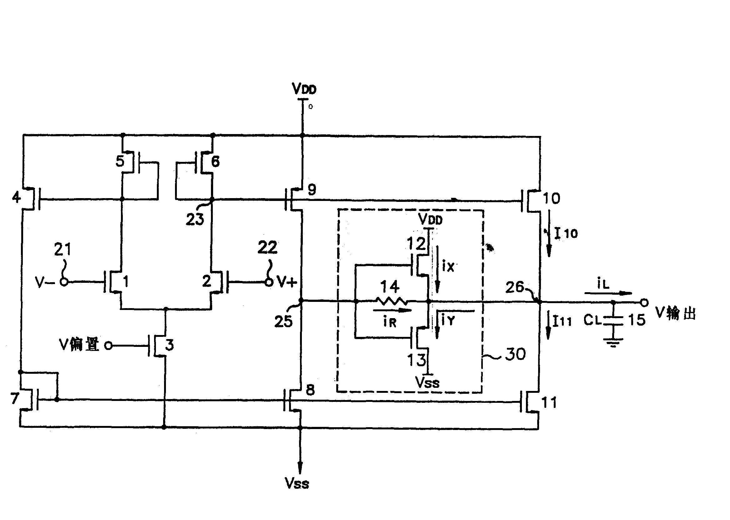
A slew rate acceleration circuit for increasing slew rate in an operational amplifier or comparator without increasing power consumption is disclosed herein. In a preferred embodiment, an operational amplifier with a differential amplifier and a first pull-up transistor 10 The amplifier includes: a first input terminal 25, a second pull-up transistor 9, a second output terminal 26 connected to one end of the channel of the first pull-up transistor 10, a common current path, a pull-up current path and a pull-up current path. The current stabilizing device 30 of the current path includes a first pull transistor 11 and a second pull transistor 8 .
Description
本发明涉及运算放大器或比较器,更具体地说,涉及能提高运算放大器的转换速率(作为输入信号的函数的输出信号的响应速度)并且在输出端有容性负载等等的电路。Field of the Invention This invention relates to operational amplifiers or comparators, and more particularly, to circuits that increase the slew rate (response speed of an output signal as a function of an input signal) of an operational amplifier and have capacitive loads at the output, etc.
大多数电子线路广泛地采用运算放大器或比较器,它们通过对反向输入端和非反向输入端上的输入信号的和、减或差分放大产生输出信号。在这种运算放大器中,首先必须确立作为输入信号的一个函数的输出信号的响应,其程度对电子线路的特性和可靠性具有重大影响。具体讲,在一个用于半导体存贮装置等的比较器中,如果响应速度慢,除将导致数据存取速度慢以外,还会引起以高速运行的存贮装置的误操作。Most electronic circuits make extensive use of operational amplifiers or comparators, which produce output signals by summing, subtracting, or differentially amplifying input signals on inverting and non-inverting inputs. In such operational amplifiers, it is first necessary to establish the response of the output signal as a function of the input signal, the extent of which has a significant effect on the characteristics and reliability of the electronic circuit. Specifically, in a comparator used in a semiconductor memory device or the like, if the response speed is slow, in addition to causing a slow data access speed, it may cause malfunction of the memory device operating at a high speed.
图1以电路图形式示出已有技术的比较器(或运算放大器)。如图1所示,将发现比较器与N沟道输入型差分放大器具有相同的结构。因此,当第一输入端21的电位高于第二输入端22的电位时,P型金属氧化物半导体(MOS)晶体管4和5以及N型MOS晶体管7和11导通,于是,将第二输出端24的电位降低。与此相反,如果第二输入端22的电位高于第一输入端21的电位,电源电压VDD通过-P型MOS晶体管10对第二输出端24充电。在此情况下,第一输出端23的电压增益AVO1和第二输出端24的电压增益AVO2分别计算如下:Figure 1 shows a prior art comparator (or operational amplifier) in circuit diagram form. As shown in Fig. 1, it will be found that the comparator has the same structure as the N-channel input type differential amplifier. Therefore, when the potential of the
VVO1=gm2/gm6 V VO1 = gm 2 /gm 6
VVO2={gm1(S10/S6)}/(gdS10+gdS11)V VO2 = {gm 1 (S 10 /S 6 )}/(gdS 10 +gdS 11 )
其中,gm1、gm2和gm6分别为N型MOS晶体管1和2及P型MOS晶体管6的跨导,gds为沟道导纳,s为沟道的宽度与长度的比率。Among them, gm 1 , gm 2 and gm 6 are the transconductances of the N-
在输出电压VOUT正向增长后,当拉曳电流I11经N型MOS晶体管11从第二输出端24流入地电压端VSS时,转换速率SR在第二输出端子24上变为最大值为“0”。在输出电压负向增长后,当上牵电流I10从电源电压端VDD经P型MOS晶体管10流入第二输出端24时,转换速率SR在第二输出端24上变为最大值为“0”。After the output voltage V OUT increases positively, when the pull current I 11 flows from the
然而,在第二输出端24,存在由寄生电容15产生的负载电容量CL,它使得负载电流iL流动。负载电容量CL和负载电流iL对在第二输出端子24的电位从逻辑“低”变为逻辑“高”或从逻辑“高”变为逻辑“低”时转换速率SR产生重大影响。详细地讲,转换速率SR相对于时间而被定义作为输出电压VOUT的差分系数,另一方面,负载电流iL表示从上牵电流I10中减去拉曳电流I11后的值。这样,转换速率SR可表示如下:However, at the
SR=|dVOUT/dt|=|iL/CL|=|(I10-I11)/CL|SR=|dV OUT /dt|=|i L /C L |=|(I 10 -I 11 )/C L |
如转换速率SR的表达式,为了增加转换速率SR(或对作为输入信号的函数具有输出信号的快速响应速度),负载电容量CL应当减小或使负载电流iL加大。负载电容量CL不可被改变,因为负载电容作为一个寄生元件,在电路结构中具有其固定值,但却可以通过增加P型MOS晶体管10或N型MOS晶体管11的规格来增加负载电流iL。然而,在输出上增加MOS晶体管10和11的规格将导致不希望的在电路功耗上的增加。As the expression for the slew rate SR, in order to increase the slew rate SR (or have a fast response speed of the output signal as a function of the input signal), the load capacitance C L should be decreased or the load current i L should be increased. The load capacitance C L cannot be changed, because the load capacitance as a parasitic element has its fixed value in the circuit structure, but the load current i L can be increased by increasing the specification of the P-
本发明的目的在于提供一种电路,该电路能够提高转换速率而不会增加在比较器的输出端等等上的功耗。It is an object of the present invention to provide a circuit capable of increasing the slew rate without increasing the power consumption at the output terminal of the comparator or the like.
根据本发明的一个方面,一个具有一差分放大器和一栅极联到差分放大器输出端上的第一上牵晶体管的运算放大器,包括:一第一输出端;一栅极联到差分放大器输出端,沟道联在电源电压端和第一输出端间的第二上牵晶体管;一个联到第一上牵晶体管沟道任何一端上的第二输出端;一个联在第一输出端和第二输出端之间并具有公共电流通路、一个上牵电流通路和一个拉曳电流通路的电流稳定装置;一其沟道联在第二输出端与地电压端之间的第一拉曳晶体管;以及一其沟道联在第一输出端与地电压端子之间的第二拉曳晶体管。According to one aspect of the present invention, an operational amplifier having a differential amplifier and a first pull-up transistor whose gate is connected to the output of the differential amplifier includes: a first output; a gate connected to the output of the differential amplifier , the channel is connected to the second pull-up transistor between the power supply voltage terminal and the first output terminal; one is connected to the second output terminal on either end of the channel of the first pull-up transistor; one is connected to the first output terminal and the second output terminal a current stabilizing device between the output terminals and having a common current path, a pulling current path and a pulling current path; a first pulling transistor whose channel is connected between the second output terminal and the ground voltage terminal; and A second pull-up transistor whose channel is connected between the first output terminal and the ground voltage terminal.
本发明的优点及特征将在以下借助于附图的详细描述中变得更加清楚:Advantages and features of the present invention will become clearer in the following detailed description with the aid of the accompanying drawings:
图1示出已有技术的比较器(或运算放大器)的电路图;Figure 1 shows a circuit diagram of a prior art comparator (or operational amplifier);
图2示出根据本发明的比较器(或运算放大器)的优选实施例的电路图;Figure 2 shows a circuit diagram of a preferred embodiment of a comparator (or operational amplifier) according to the present invention;
图3示出根据本发明的操作波形图。Fig. 3 shows an operation waveform diagram according to the present invention.
图2中,与图1中所示元件具有相同结构的元件标以相同的参考号。如图2所示,P型MOS晶体管9的栅极联到差分放大器的一个输出端23上,其沟道联在电源端VDD和第一输出端25之间。N型MOS晶体管8其栅极联到N型MOS晶体管7的栅极,其沟道联在第一输出端25和地电压端VSS之间。电流稳定电路30包含一N型MOS晶体管12、一P型MOS晶体管13及一电阻器14,该电流稳定电路30是联在第一输出端25和第二输出端26之间的,第二输出端26与图1中第二输出端24对应。N型MOS晶体管12的栅极联到第一输出端25,其沟道串在电源端VDD与第二输出端26之间。P型MOS晶体管13的栅极联到第一输出端25,其沟通联在第二输出端26与地电压端VSS之间。电阻14串在第一输出端25与第二输出端26之间。在图2所示电路中,应当注意:用于上牵的P型MOS晶体管9和10规格相同,并且用于拉曳的N型MOS晶体管8和11规格也相同。In FIG. 2, elements having the same structure as those shown in FIG. 1 are assigned the same reference numerals. As shown in FIG. 2 , the gate of the P-
在图3中示出在第一输出端子25上的输入波形31和波形32以及在第二输出端子26上的波形33。假定作为“第一输入信号”的输入信号为逻辑低,即“0”电平,且被加到第一输入端21,作为“第二输入信号”诸如图3输入波形31的信号被加到第二输入端子22上。由于第二输入信号的电位高于第一输入信号的电位,则差分放大器的输出端23的电位变为逻辑低。因而,用于上牵的P型MOS晶体管9和10导通,于是,对第一输入端子25和第二输入端子26充电直达到电源电压VDD的电平。在这种情况下,如果在第二输出端26上没有电容15,则第一输出端子25和第二输出端子26之间电压彼此相同,且电流不会在第一输出端子25和第二输出端子26之间流动。但是,如上所述,不可避免由寄生电容15产生的负载电容量CL在第二输出端26上的存在。因此,在第一输出端25由负载电容量CL产生如图3的波形32的电压、在第二输出端26产生如图3的波形33的电压。第二输出端26的波形33具有较平缓的陡度,即其转换速率与第一输出端的波形32相比更缓和。这一点是由负载电容CL充电时间决定的。也就是说,在时间t1,第一输出端25的电位高于第二输出端26的电位△V。如果电位差△V大于N型MOS晶体管12的阈值电压,则N型MOS晶体管12导通,电流iX流入第二输出端26直到第一和第二输出端子25和26的电位相等为止。此外,由在电阻14中第一输出端子25与第二输出端子26之间的电位差产生的电流iR流入第二输出端26。即,流入第二输出端子26的电流数量变为(I10-I11)+iX+iR。流入第二输出端26的电流量与图1之中的相比增加了(iX+iR)。增加输出电流的结果使电容15的充电时间缩短较多,由此提高了转换速率。依相同途径,如果第二输入信号的电位低于为逻辑“0”电平的第一输入信号的电位,则流入地电压端VSS的电流为经P型MOS晶体管13流入的电流、其方向与上述电流iR相反的经电阻器14流入第一输出端25的电流与拉曳电流i11的和电流iY。其中经电阻器14流入第一输出端子25的电流方向取决于第一输出端子25与所述第二输出端子26间的电位差。因此,对负载电容CL的充电时间缩短较多,故提高了转换速率。FIG. 3 shows an
结果,由于第二输出端子26的波形33依箭头方向移动,作为输入波形31的函数的输出信号响应速度(或转换速率)加快。As a result, the response speed (or slew rate) of the output signal as a function of the
如上所述,在运算放大器或比较器中,输出信号的转换速率提高而无需增加电路的功率储备。As mentioned above, in an operational amplifier or comparator, the slew rate of the output signal is increased without increasing the power reserve of the circuit.
本发明已被具体示出,并参考采用N沟道输入型比较器的优选实施例加以描述了。但是,既使是采用P沟道输入型比较器,或采用图3所示输入波形31那样的信号作为第一输入信号,并将第二输入信号设置为逻辑“0”电平,而那些本技术领域的人应当知道,操作和通过对优选实施例的描述而达到的目的仍可被实现。The present invention has been shown and described with reference to a preferred embodiment using an N-channel input type comparator. However, even if a P-channel input comparator is used, or a signal such as the
Claims (8)
Applications Claiming Priority (2)
| Application Number | Priority Date | Filing Date | Title |
|---|---|---|---|
| KR1019910012922A KR940001816B1 (en) | 1991-07-26 | 1991-07-26 | Slew Rate Speed Sup Circuit |
| KR12922/91 | 1991-07-26 |
Publications (2)
| Publication Number | Publication Date |
|---|---|
| CN1069152A true CN1069152A (en) | 1993-02-17 |
| CN1028824C CN1028824C (en) | 1995-06-07 |
Family
ID=19317878
Family Applications (1)
| Application Number | Title | Priority Date | Filing Date |
|---|---|---|---|
| CN91109930A Expired - Fee Related CN1028824C (en) | 1991-07-26 | 1991-10-19 | Slew Rate Acceleration Circuit |
Country Status (6)
| Country | Link |
|---|---|
| US (1) | US5223753A (en) |
| JP (1) | JPH0738538B2 (en) |
| KR (1) | KR940001816B1 (en) |
| CN (1) | CN1028824C (en) |
| GB (1) | GB2258107B (en) |
| TW (1) | TW209323B (en) |
Cited By (3)
| Publication number | Priority date | Publication date | Assignee | Title |
|---|---|---|---|---|
| CN1055845C (en) * | 1995-06-05 | 2000-08-30 | 金纪前 | Dieda Huoxuesan powder for curing fracture and injury |
| CN102384999A (en) * | 2010-08-30 | 2012-03-21 | 深圳艾科创新微电子有限公司 | High-speed transmission event detection method and circuit |
| CN108259007A (en) * | 2017-12-29 | 2018-07-06 | 思瑞浦微电子科技(苏州)股份有限公司 | Enhancing circuit applied to amplifier conversion rate |
Families Citing this family (26)
| Publication number | Priority date | Publication date | Assignee | Title |
|---|---|---|---|---|
| JPH05312850A (en) * | 1992-05-12 | 1993-11-26 | Nec Ic Microcomput Syst Ltd | Semiconductor integrated circuit |
| DE4222170C1 (en) * | 1992-07-06 | 1993-09-23 | Siemens Ag, 80333 Muenchen, De | |
| US5278467A (en) * | 1992-07-14 | 1994-01-11 | Intel Corporation | Self-biasing input stage for high-speed low-voltage communication |
| US5488321A (en) * | 1993-04-07 | 1996-01-30 | Rambus, Inc. | Static high speed comparator |
| AU1841895A (en) * | 1994-02-15 | 1995-08-29 | Rambus Inc. | Delay-locked loop |
| US5614852A (en) * | 1995-08-08 | 1997-03-25 | Harris Corp. | Wide common mode range comparator and method |
| SG54327A1 (en) * | 1996-04-27 | 1998-11-16 | Motorola Inc | Monolithic high voltage driver circuit |
| US5754131A (en) * | 1996-07-01 | 1998-05-19 | General Electric Company | Low power delta sigma converter |
| KR100414264B1 (en) * | 1996-12-20 | 2004-04-03 | 엘지전자 주식회사 | Op amplifier for changing slew rate |
| US5959481A (en) * | 1997-02-18 | 1999-09-28 | Rambus Inc. | Bus driver circuit including a slew rate indicator circuit having a one shot circuit |
| KR19990081272A (en) * | 1998-04-28 | 1999-11-15 | 윤종용 | Output driving circuit of LCD driver source driver |
| US5939870A (en) * | 1998-09-17 | 1999-08-17 | Intel Corporation | Voltage regulator |
| US6323683B1 (en) * | 1999-08-27 | 2001-11-27 | Cypress Semiconductor Corp. | Low distortion logic level translator |
| US6326819B1 (en) * | 1999-11-15 | 2001-12-04 | General Motors Corporation | Current buffer for gate drive |
| US7012465B2 (en) * | 2001-08-07 | 2006-03-14 | Qualcomm Incorporated | Low-voltage class-AB output stage amplifier |
| US6414552B1 (en) | 2001-11-16 | 2002-07-02 | Dialog Semiconductor Gmbh | Operational transconductance amplifier with a non-linear current mirror for improved slew rate |
| WO2004015867A1 (en) * | 2002-08-08 | 2004-02-19 | Koninklijke Philips Electronics N.V. | Circuit and method for controlling the threshold voltage of transistors |
| US7301370B1 (en) * | 2003-05-22 | 2007-11-27 | Cypress Semiconductor Corporation | High-speed differential logic to CMOS translator architecture with low data-dependent jitter and duty cycle distortion |
| JP4614704B2 (en) * | 2003-07-23 | 2011-01-19 | ルネサスエレクトロニクス株式会社 | Differential amplifier, data driver and display device |
| KR100753151B1 (en) | 2005-04-22 | 2007-08-30 | 삼성전자주식회사 | Op amp for output buffer and signal processing circuit using same |
| KR100790492B1 (en) * | 2005-07-01 | 2008-01-02 | 삼성전자주식회사 | Source driver controlling slew rate and its driving method |
| CN101005273B (en) * | 2006-01-20 | 2010-06-23 | 深圳赛意法微电子有限公司 | Differential amplifier with improved conversion speed |
| KR100792432B1 (en) * | 2006-10-31 | 2008-01-10 | 주식회사 하이닉스반도체 | Operational amplifier with stable output. |
| US7771115B2 (en) * | 2007-08-16 | 2010-08-10 | Micron Technology, Inc. | Temperature sensor circuit, device, system, and method |
| CN103472882B (en) * | 2013-09-30 | 2015-04-15 | 电子科技大学 | Low dropout regulator of integrated slew rate enhancement circuit |
| US20170163226A1 (en) * | 2015-12-08 | 2017-06-08 | Skyworks Solutions, Inc. | Fast switching power amplifier, low noise amplifier, and radio frequency switch circuits |
Family Cites Families (8)
| Publication number | Priority date | Publication date | Assignee | Title |
|---|---|---|---|---|
| US4464588A (en) * | 1982-04-01 | 1984-08-07 | National Semiconductor Corporation | Temperature stable CMOS voltage reference |
| JPS6070806A (en) * | 1983-09-28 | 1985-04-22 | Hitachi Ltd | Differential amplifier circuit |
| US4614882A (en) * | 1983-11-22 | 1986-09-30 | Digital Equipment Corporation | Bus transceiver including compensation circuit for variations in electrical characteristics of components |
| JPS6121607A (en) * | 1984-07-10 | 1986-01-30 | Nec Corp | Operational amplifier using complementary misfet |
| JPS62125705A (en) * | 1985-11-26 | 1987-06-08 | Nec Corp | Operational amplifier circuit |
| US4636665A (en) * | 1985-12-02 | 1987-01-13 | Motorola, Inc. | BIMOS memory sense amplifier |
| JP2543872B2 (en) * | 1986-08-13 | 1996-10-16 | 株式会社東芝 | Amplifier circuit |
| JPH01138813A (en) * | 1987-11-26 | 1989-05-31 | Toshiba Corp | Level conversion circuit |
-
1991
- 1991-07-26 KR KR1019910012922A patent/KR940001816B1/en not_active Expired - Fee Related
- 1991-09-06 US US07/755,869 patent/US5223753A/en not_active Expired - Lifetime
- 1991-09-16 TW TW080107309A patent/TW209323B/zh active
- 1991-10-18 JP JP3270871A patent/JPH0738538B2/en not_active Expired - Fee Related
- 1991-10-19 CN CN91109930A patent/CN1028824C/en not_active Expired - Fee Related
- 1991-10-21 GB GB9122286A patent/GB2258107B/en not_active Expired - Fee Related
Cited By (5)
| Publication number | Priority date | Publication date | Assignee | Title |
|---|---|---|---|---|
| CN1055845C (en) * | 1995-06-05 | 2000-08-30 | 金纪前 | Dieda Huoxuesan powder for curing fracture and injury |
| CN102384999A (en) * | 2010-08-30 | 2012-03-21 | 深圳艾科创新微电子有限公司 | High-speed transmission event detection method and circuit |
| CN102384999B (en) * | 2010-08-30 | 2015-08-19 | 深圳艾科创新微电子有限公司 | A kind of high-speed transmission event detection method and circuit |
| CN108259007A (en) * | 2017-12-29 | 2018-07-06 | 思瑞浦微电子科技(苏州)股份有限公司 | Enhancing circuit applied to amplifier conversion rate |
| CN108259007B (en) * | 2017-12-29 | 2021-06-04 | 思瑞浦微电子科技(苏州)股份有限公司 | Enhancement circuit applied to operational amplifier conversion rate |
Also Published As
| Publication number | Publication date |
|---|---|
| JPH0738538B2 (en) | 1995-04-26 |
| KR940001816B1 (en) | 1994-03-09 |
| GB9122286D0 (en) | 1991-12-04 |
| JPH0555837A (en) | 1993-03-05 |
| US5223753A (en) | 1993-06-29 |
| GB2258107B (en) | 1995-04-19 |
| GB2258107A (en) | 1993-01-27 |
| CN1028824C (en) | 1995-06-07 |
| TW209323B (en) | 1993-07-11 |
| KR930003522A (en) | 1993-02-24 |
Similar Documents
| Publication | Publication Date | Title |
|---|---|---|
| CN1028824C (en) | Slew Rate Acceleration Circuit | |
| US7554379B2 (en) | High-speed, low-power level shifter for mixed signal-level environments | |
| US6653878B2 (en) | Low-power output controlled circuit | |
| CN1018783B (en) | transistor circuit | |
| US4972101A (en) | Noise reduction in CMOS driver using capacitor discharge to generate a control voltage | |
| KR960011964B1 (en) | Output buffer device | |
| KR940005509B1 (en) | Step-up control circuit and its output buffer circuit | |
| JPH08195631A (en) | Sense amplifier | |
| US6317000B1 (en) | Overload recovery circuit and method | |
| JP3126629B2 (en) | Operational amplifier | |
| US20030210079A1 (en) | Input/output buffer having reduced skew and methods of operation | |
| JP2968826B2 (en) | Current mirror type amplifier circuit and driving method thereof | |
| JPH0456400B2 (en) | ||
| KR0144900B1 (en) | Input buffer of low power supply semiconductor device | |
| US5532628A (en) | Fast comparator circuit | |
| KR100280492B1 (en) | Integrator input circuit | |
| US5045718A (en) | Circuit for detecting power supply voltage variation | |
| JP2003078367A (en) | Amplifier circuit | |
| US5773992A (en) | Output buffer circuit capable of supressing ringing | |
| US5825212A (en) | High speed single ended bit line sense amplifier | |
| JPH10326492A (en) | Amplifier | |
| JP2917356B2 (en) | Semiconductor output circuit | |
| JPH04306915A (en) | Level conversion circuit | |
| JP2930227B2 (en) | Output buffer circuit of semiconductor integrated circuit | |
| JPH0347012B2 (en) |
Legal Events
| Date | Code | Title | Description |
|---|---|---|---|
| C06 | Publication | ||
| PB01 | Publication | ||
| C10 | Entry into substantive examination | ||
| SE01 | Entry into force of request for substantive examination | ||
| C14 | Grant of patent or utility model | ||
| GR01 | Patent grant | ||
| C15 | Extension of patent right duration from 15 to 20 years for appl. with date before 31.12.1992 and still valid on 11.12.2001 (patent law change 1993) | ||
| OR01 | Other related matters | ||
| C19 | Lapse of patent right due to non-payment of the annual fee | ||
| CF01 | Termination of patent right due to non-payment of annual fee |