CN106918877B - Optical engine for data communication - Google Patents
Optical engine for data communication Download PDFInfo
- Publication number
- CN106918877B CN106918877B CN201610879292.XA CN201610879292A CN106918877B CN 106918877 B CN106918877 B CN 106918877B CN 201610879292 A CN201610879292 A CN 201610879292A CN 106918877 B CN106918877 B CN 106918877B
- Authority
- CN
- China
- Prior art keywords
- lens group
- optical
- array
- arrays
- bridge
- Prior art date
- Legal status (The legal status is an assumption and is not a legal conclusion. Google has not performed a legal analysis and makes no representation as to the accuracy of the status listed.)
- Active
Links
- 230000003287 optical effect Effects 0.000 title claims abstract description 167
- 238000004891 communication Methods 0.000 title claims abstract description 22
- 239000004065 semiconductor Substances 0.000 claims abstract description 57
- 239000002184 metal Substances 0.000 claims abstract description 34
- 239000000758 substrate Substances 0.000 claims abstract description 28
- 239000013307 optical fiber Substances 0.000 claims abstract description 18
- 239000000835 fiber Substances 0.000 claims abstract description 15
- 238000003491 array Methods 0.000 claims description 55
- 230000005693 optoelectronics Effects 0.000 claims description 34
- 238000003825 pressing Methods 0.000 claims description 4
- 230000008878 coupling Effects 0.000 description 5
- 238000010168 coupling process Methods 0.000 description 5
- 238000005859 coupling reaction Methods 0.000 description 5
- 230000005540 biological transmission Effects 0.000 description 4
- 238000010586 diagram Methods 0.000 description 3
- 238000012986 modification Methods 0.000 description 3
- 230000004048 modification Effects 0.000 description 3
- 238000000034 method Methods 0.000 description 2
- 238000013461 design Methods 0.000 description 1
- 238000011161 development Methods 0.000 description 1
- 238000004519 manufacturing process Methods 0.000 description 1
- 238000003860 storage Methods 0.000 description 1
- 238000006467 substitution reaction Methods 0.000 description 1
Images


Classifications
-
- G—PHYSICS
- G02—OPTICS
- G02B—OPTICAL ELEMENTS, SYSTEMS OR APPARATUS
- G02B6/00—Light guides; Structural details of arrangements comprising light guides and other optical elements, e.g. couplings
- G02B6/24—Coupling light guides
- G02B6/42—Coupling light guides with opto-electronic elements
- G02B6/4201—Packages, e.g. shape, construction, internal or external details
- G02B6/4204—Packages, e.g. shape, construction, internal or external details the coupling comprising intermediate optical elements, e.g. lenses, holograms
-
- G—PHYSICS
- G02—OPTICS
- G02B—OPTICAL ELEMENTS, SYSTEMS OR APPARATUS
- G02B6/00—Light guides; Structural details of arrangements comprising light guides and other optical elements, e.g. couplings
- G02B6/24—Coupling light guides
- G02B6/42—Coupling light guides with opto-electronic elements
- G02B6/4201—Packages, e.g. shape, construction, internal or external details
- G02B6/4219—Mechanical fixtures for holding or positioning the elements relative to each other in the couplings; Alignment methods for the elements, e.g. measuring or observing methods especially used therefor
- G02B6/4228—Passive alignment, i.e. without a detection of the degree of coupling or the position of the elements
- G02B6/423—Passive alignment, i.e. without a detection of the degree of coupling or the position of the elements using guiding surfaces for the alignment
-
- G—PHYSICS
- G02—OPTICS
- G02B—OPTICAL ELEMENTS, SYSTEMS OR APPARATUS
- G02B6/00—Light guides; Structural details of arrangements comprising light guides and other optical elements, e.g. couplings
- G02B6/24—Coupling light guides
- G02B6/26—Optical coupling means
- G02B6/32—Optical coupling means having lens focusing means positioned between opposed fibre ends
-
- G—PHYSICS
- G02—OPTICS
- G02B—OPTICAL ELEMENTS, SYSTEMS OR APPARATUS
- G02B6/00—Light guides; Structural details of arrangements comprising light guides and other optical elements, e.g. couplings
- G02B6/24—Coupling light guides
- G02B6/42—Coupling light guides with opto-electronic elements
- G02B6/4201—Packages, e.g. shape, construction, internal or external details
- G02B6/4204—Packages, e.g. shape, construction, internal or external details the coupling comprising intermediate optical elements, e.g. lenses, holograms
- G02B6/4214—Packages, e.g. shape, construction, internal or external details the coupling comprising intermediate optical elements, e.g. lenses, holograms the intermediate optical element having redirecting reflective means, e.g. mirrors, prisms for deflecting the radiation from horizontal to down- or upward direction toward a device
-
- G—PHYSICS
- G02—OPTICS
- G02B—OPTICAL ELEMENTS, SYSTEMS OR APPARATUS
- G02B6/00—Light guides; Structural details of arrangements comprising light guides and other optical elements, e.g. couplings
- G02B6/24—Coupling light guides
- G02B6/42—Coupling light guides with opto-electronic elements
- G02B6/4201—Packages, e.g. shape, construction, internal or external details
- G02B6/4219—Mechanical fixtures for holding or positioning the elements relative to each other in the couplings; Alignment methods for the elements, e.g. measuring or observing methods especially used therefor
-
- G—PHYSICS
- G02—OPTICS
- G02B—OPTICAL ELEMENTS, SYSTEMS OR APPARATUS
- G02B6/00—Light guides; Structural details of arrangements comprising light guides and other optical elements, e.g. couplings
- G02B6/24—Coupling light guides
- G02B6/42—Coupling light guides with opto-electronic elements
- G02B6/4201—Packages, e.g. shape, construction, internal or external details
- G02B6/4219—Mechanical fixtures for holding or positioning the elements relative to each other in the couplings; Alignment methods for the elements, e.g. measuring or observing methods especially used therefor
- G02B6/4236—Fixing or mounting methods of the aligned elements
- G02B6/4244—Mounting of the optical elements
-
- G—PHYSICS
- G02—OPTICS
- G02B—OPTICAL ELEMENTS, SYSTEMS OR APPARATUS
- G02B6/00—Light guides; Structural details of arrangements comprising light guides and other optical elements, e.g. couplings
- G02B6/24—Coupling light guides
- G02B6/42—Coupling light guides with opto-electronic elements
- G02B6/4201—Packages, e.g. shape, construction, internal or external details
- G02B6/4246—Bidirectionally operating package structures
-
- G—PHYSICS
- G02—OPTICS
- G02B—OPTICAL ELEMENTS, SYSTEMS OR APPARATUS
- G02B6/00—Light guides; Structural details of arrangements comprising light guides and other optical elements, e.g. couplings
- G02B6/24—Coupling light guides
- G02B6/42—Coupling light guides with opto-electronic elements
- G02B6/4201—Packages, e.g. shape, construction, internal or external details
- G02B6/4249—Packages, e.g. shape, construction, internal or external details comprising arrays of active devices and fibres
-
- G—PHYSICS
- G02—OPTICS
- G02B—OPTICAL ELEMENTS, SYSTEMS OR APPARATUS
- G02B6/00—Light guides; Structural details of arrangements comprising light guides and other optical elements, e.g. couplings
- G02B6/24—Coupling light guides
- G02B6/42—Coupling light guides with opto-electronic elements
- G02B6/4201—Packages, e.g. shape, construction, internal or external details
- G02B6/4249—Packages, e.g. shape, construction, internal or external details comprising arrays of active devices and fibres
- G02B6/425—Optical features
-
- G—PHYSICS
- G02—OPTICS
- G02B—OPTICAL ELEMENTS, SYSTEMS OR APPARATUS
- G02B6/00—Light guides; Structural details of arrangements comprising light guides and other optical elements, e.g. couplings
- G02B6/24—Coupling light guides
- G02B6/42—Coupling light guides with opto-electronic elements
- G02B6/4201—Packages, e.g. shape, construction, internal or external details
- G02B6/4256—Details of housings
- G02B6/4257—Details of housings having a supporting carrier or a mounting substrate or a mounting plate
- G02B6/4259—Details of housings having a supporting carrier or a mounting substrate or a mounting plate of the transparent type
-
- G—PHYSICS
- G02—OPTICS
- G02B—OPTICAL ELEMENTS, SYSTEMS OR APPARATUS
- G02B6/00—Light guides; Structural details of arrangements comprising light guides and other optical elements, e.g. couplings
- G02B6/24—Coupling light guides
- G02B6/42—Coupling light guides with opto-electronic elements
- G02B6/4201—Packages, e.g. shape, construction, internal or external details
- G02B6/4274—Electrical aspects
- G02B6/428—Electrical aspects containing printed circuit boards [PCB]
-
- G—PHYSICS
- G02—OPTICS
- G02B—OPTICAL ELEMENTS, SYSTEMS OR APPARATUS
- G02B6/00—Light guides; Structural details of arrangements comprising light guides and other optical elements, e.g. couplings
- G02B6/24—Coupling light guides
- G02B6/42—Coupling light guides with opto-electronic elements
- G02B6/43—Arrangements comprising a plurality of opto-electronic elements and associated optical interconnections
-
- G—PHYSICS
- G02—OPTICS
- G02B—OPTICAL ELEMENTS, SYSTEMS OR APPARATUS
- G02B6/00—Light guides; Structural details of arrangements comprising light guides and other optical elements, e.g. couplings
- G02B6/24—Coupling light guides
- G02B6/42—Coupling light guides with opto-electronic elements
- G02B6/4201—Packages, e.g. shape, construction, internal or external details
- G02B6/4219—Mechanical fixtures for holding or positioning the elements relative to each other in the couplings; Alignment methods for the elements, e.g. measuring or observing methods especially used therefor
- G02B6/4236—Fixing or mounting methods of the aligned elements
- G02B6/424—Mounting of the optical light guide
-
- G—PHYSICS
- G02—OPTICS
- G02B—OPTICAL ELEMENTS, SYSTEMS OR APPARATUS
- G02B6/00—Light guides; Structural details of arrangements comprising light guides and other optical elements, e.g. couplings
- G02B6/24—Coupling light guides
- G02B6/42—Coupling light guides with opto-electronic elements
- G02B6/4292—Coupling light guides with opto-electronic elements the light guide being disconnectable from the opto-electronic element, e.g. mutually self aligning arrangements
Landscapes
- Physics & Mathematics (AREA)
- General Physics & Mathematics (AREA)
- Optics & Photonics (AREA)
- Optical Couplings Of Light Guides (AREA)
Abstract
一种用于数据通信的光学引擎包括:基板;安装在基板上的光学半导体器件阵列;安装在基板上的器件透镜组,所述器件透镜组有腔体,用于容纳所述光学半导体器件阵列;跨接透镜组,所述跨接透镜组联接在所述器件透镜组的上表面处;光纤阵列,所述光纤阵列安装在所述跨接透镜组上,与所述光学半导体器件阵列光学地联接。所述跨接透镜组借助于对准柱和对准凹槽与所述器件透镜组对准。金属锁用于将所述跨接透镜组固定在所述器件透镜组上。
An optical engine for data communication includes: a substrate; an optical semiconductor device array installed on the substrate; and a device lens group installed on the substrate, the device lens group having a cavity for accommodating the optical semiconductor device array ; Jumper lens group, the jumper lens group is connected to the upper surface of the device lens group; Optical fiber array, the fiber array is installed on the jumper lens group, and is optically connected to the optical semiconductor device array; join. The jumper lens set is aligned with the device lens set by means of alignment posts and alignment grooves. The metal lock is used to fix the jumper lens group on the device lens group.
Description
技术领域technical field
本申请涉及用于数据通信的光学引擎。The present application relates to optical engines for data communications.
背景技术Background technique
由于移动数据应用、云计算和物联网(Internet of Things,IoT)的日益普及,对数据中心内的切换能力和计算能力的需求日益增长。这使得对于交换机、计算节点和存储设备之间的数据交换的容量和密集度的需求日益增长。高速光收发机和基于短距离多模光纤的有源光缆(AOC)的生产是用于解决这类需求的方案。随着数据中心交换机的每端口的数据速率当今达到100Gb/s且很快将提高并超过400Gb/s和1Tb/s,需要可扩展的光学引擎来促进具有成本效益优势的高速且高密集度的多模(MM)光互连方案的快速发展。随着数据中心的规模变得更大,传输距离会增长,例如超过500米。因此,存在极大需求来生产可扩展的光学引擎,以促进实现低成本、高速且高密集度的光收发机和应答机方案,从而应对现代数据中心互连需求的挑战。Due to the increasing popularity of mobile data applications, cloud computing, and the Internet of Things (IoT), there is an increasing demand for switching capabilities and computing power within data centers. This has created an ever-increasing demand for the capacity and density of data exchange between switches, compute nodes, and storage devices. The production of high-speed optical transceivers and active optical cables (AOCs) based on short-reach multimode fibers are solutions to these needs. With per-port data rates of data center switches reaching 100Gb/s today and will soon increase beyond 400Gb/s and 1Tb/s, scalable optical engines are needed to facilitate cost-effective high-speed and high-density Rapid development of multimode (MM) optical interconnect solutions. As the size of the data center becomes larger, the transmission distance grows, for example, over 500 meters. Therefore, there is a great need to produce scalable optical engines to facilitate low-cost, high-speed, and high-density optical transceiver and transponder solutions to meet the challenges of modern data center interconnect requirements.
上述对背景技术的描述用以帮助理解用于数据通信的光学引擎,但是不应当被认为是描述或设立关于用于数据通信的光学引擎的现有技术。The above description of the background art is intended to aid in the understanding of optical engines for data communications, but should not be considered to describe or establish prior art regarding optical engines for data communications.
发明内容SUMMARY OF THE INVENTION
按照一方面,本申请提供了一种用于数据通信的光学引擎,包括:设定纵轴线的基板;横向地安装在所述基板上的光学半导体器件阵列,所述光学半导体器件选自包括发射型光电组件、接收型光电组件、以及发射型光电组件和接收型光电组件的组合的组;器件透镜组,所述器件透镜组安装在所述基板上且形成腔体,所述腔体用于容纳所述光学半导体器件的阵列;两个器件透镜阵列分别形成在所述器件透镜组的两个相对侧上;跨接透镜组,所述跨接透镜组联接在所述器件透镜组的上表面处,其中,所述跨接透镜组具有第一对准部件以及透镜阵列,所述第一对准部件配置成可与形成在所述器件透镜组上的第二对准部件紧密地接合,以促使所述跨接透镜组与所述器件透镜组的精确的光对准,所述透镜阵列形成在相对于所述基板成45度角布置的内部全反射表面上;光纤阵列,所述光纤阵列安装在所述跨接透镜组上,借助于所述器件透镜组的一个所述器件透镜阵列和所述跨接透镜组的所述透镜阵列与所述光学半导体器件的阵列光学地联接;以及金属锁,所述金属锁用于将所述跨接透镜组固定在所述器件透镜组表面的特定位置上,其中,所述金属锁包括第一部分和第二部分,所述第一部分可拆卸地与所述器件透镜组联接,所述第二部分接触并使所述跨接透镜组固定于所述器件透镜组。在一个实施例中,所述光纤阵列可以布置为平行于所述基板。According to one aspect, the present application provides an optical engine for data communication, comprising: a substrate setting a longitudinal axis; an array of optical semiconductor devices laterally mounted on the substrate, the optical semiconductor devices selected from the group consisting of transmitting Type optoelectronic components, receiving type optoelectronic components, and a combination of emission type optoelectronic components and receiving type optoelectronic components; device lens group, the device lens group is mounted on the substrate and forms a cavity, the cavity is used for an array housing the optical semiconductor devices; two device lens arrays are respectively formed on two opposite sides of the device lens group; a bridge lens group coupled to the upper surface of the device lens group where the bridge lens group has a first alignment member and a lens array, the first alignment member being configured to be closely engageable with a second alignment member formed on the device lens group to Facilitates precise optical alignment of the spanning lens group with the device lens group, the lens array formed on a total internal reflection surface disposed at a 45 degree angle with respect to the substrate; an optical fiber array, the optical fiber array mounted on the bridge lens set, optically coupled with the array of optical semiconductor devices by means of one of the device lens arrays of the device lens set and the lens array of the bridge lens set; and a metal A lock, the metal lock is used to fix the spanning lens group on a specific position on the surface of the device lens group, wherein the metal lock includes a first part and a second part, the first part is detachably connected with The device lens group is coupled, and the second portion contacts and fixes the bridge lens group to the device lens group. In one embodiment, the fiber array may be arranged parallel to the substrate.
在一个实施例中,所述内部全反射表面可以在接收光学信号时将来自所述光纤阵列的光反射到所述光学半导体器件的阵列,以及在发送光学信号时将来自所述光学半导体器件的阵列的光反射到所述光纤阵列。所述跨接透镜组的所述透镜阵列可以是椭圆形透镜阵列。In one embodiment, the total internal reflection surface may reflect light from the optical fiber array to the array of optical semiconductor devices when receiving optical signals, and reflect light from the optical semiconductor devices when transmitting optical signals Light from the array is reflected to the fiber array. The lens array of the spanning lens group may be an elliptical lens array.
在一个实施例中,一个所述器件透镜阵列可以用于发送光学信号,另一个所述器件透镜阵列可以用于接收光学信号。In one embodiment, one of the device lens arrays may be used to transmit optical signals and the other of the device lens arrays may be used to receive optical signals.
在一个实施例中,所述第二对准部件可以为两对对准凹槽的形式,所述两对对准凹槽分别形成在所述器件透镜组的两个相对侧上,每对对准凹槽用于容纳所述跨接透镜组的所述第一对准部件,所述第一对准部件可以为形成在所述跨接透镜组上的一对对准柱的形式。In one embodiment, the second alignment member may be in the form of two pairs of alignment grooves, the two pairs of alignment grooves are respectively formed on two opposite sides of the device lens group, each pair of An alignment groove is used to accommodate the first alignment member of the spanning lens group, which may be in the form of a pair of alignment posts formed on the spanning lens group.
在一个实施例中,所述的光学引擎可以包括:两个光学半导体器件的阵列,所述两个光学半导体器件的阵列布置成并排式排列且与两个并排式器件透镜组光学地关联;以及两个并排式光纤阵列,所述两个并排式光纤阵列分别安装在两个并排式跨接透镜组上且与所述两个光学半导体器件的阵列光学地联接。In one embodiment, the optical engine may comprise: an array of two optical semiconductor devices arranged in a side-by-side arrangement and optically associated with two side-by-side device lens groups; and Two side-by-side fiber arrays are mounted on the two side-by-side jumper lens groups, respectively, and are optically coupled with the two arrays of optical semiconductor devices.
在一个实施例中,所述的光学引擎可以包括:两个光学半导体器件的阵列,所述两个光学半导体器件的阵列垂直于所述基板的所述纵轴线、分别沿着所述腔体的两个相对侧延伸;以及两个首尾相连的光纤阵列,所述两个首尾相连的光纤阵列分别安装在两个首尾相连的跨接透镜组上且与所述两个光学半导体器件的阵列光学地联接。In one embodiment, the optical engine may include: two arrays of optical semiconductor devices, the arrays of the two optical semiconductor devices are perpendicular to the longitudinal axis of the substrate, along the longitudinal axis of the cavity, respectively. two opposite side extensions; and two end-to-end optical fiber arrays mounted on two end-to-end spanning lens groups, respectively, and optically connected to the two arrays of optical semiconductor devices join.
在一个实施例中,所述的光学引擎可以包括:两个光学半导体器件的阵列,所述两个光学半导体器件的阵列分别沿着所述器件透镜组腔体中的两个相对侧延伸;以及安装在两个跨接透镜组上的两个光纤阵列,其中,所述跨接透镜组包括透镜阵列,所述透镜阵列分别形成在相对于所述基板成45度角布置的两个内部全反射表面上,且其中,所述两个光纤阵列分别借助于所述处于两个跨接透镜组上的两个透镜阵列而与所述两个光学半导体器件的阵列光学地联接。In one embodiment, the optical engine may comprise: two arrays of optical semiconductor devices extending along two opposite sides of the device lens group cavity, respectively; and Two fiber arrays mounted on two spanning lens groups, wherein the spanning lens groups include lens arrays formed respectively in two total internal reflections arranged at a 45 degree angle with respect to the substrate Superficially, and wherein, the two optical fiber arrays are optically coupled with the two arrays of optical semiconductor devices by means of the two lens arrays on the two bridge lens groups, respectively.
在一个实施例中,所述发射型光电组件可以是垂直腔面发射激光器;且可以连接到驱动集成电路。In one embodiment, the emissive optoelectronic component may be a vertical cavity surface emitting laser; and may be connected to a driver integrated circuit.
在一个实施例中,所述接收型光电组件可以是光电二极管;且可以连接到驱动集成电路。In one embodiment, the receiver-type optoelectronic component may be a photodiode; and may be connected to a driver integrated circuit.
在一个实施例中,所述跨接透镜组的所述第一对准部件可以为两个对准柱的形式,且所述器件透镜组的所述第二对准部件为两个对准凹槽的形式,所述两个对准凹槽分别形成在所述器件透镜组的两个相对侧上,由此所述跨接透镜组的所述两个对准柱分别能够插入到所述器件透镜组的所述两个对准凹槽中。In one embodiment, the first alignment features of the bridging lens group may be in the form of two alignment posts, and the second alignment features of the device lens group are two alignment recesses In the form of a groove, the two alignment grooves are respectively formed on two opposite sides of the device lens group, whereby the two alignment posts of the bridge lens group can be respectively inserted into the device into the two alignment grooves of the lens group.
在一个实施例中,所述金属锁可以包括:(i)两个锁槽,所述两个锁槽形成在所述金属锁的中间部分处的两个相对侧上,用于与两个锁勾接合,所述两个锁勾形成在所述器件透镜组上的中间部分处;(ii)两个柔性臂,所述两个柔性臂从所述中间部分的第一端处开始纵向延伸,至少一个突出部形成在每个柔性臂的底部表面上,用于与所述跨接透镜组接触,将其按压在所述器件透镜组上,两个内弯端部形成在两个所述柔性臂的自由端上,用于紧靠所述跨接透镜组的端部表面;以及(iii)两个U形弹簧,所述两个U形弹簧从所述中间部分的第二端开始延伸,用于接触并使所述器件透镜组偏向所述基板。所述金属锁还包括两个突出部,所述两个突出部分别从所述两个锁槽开始纵向延伸,以于解锁时促进所述金属锁脱离所述器件透镜组。In one embodiment, the metal lock may include: (i) two lock grooves formed on two opposite sides at a middle portion of the metal lock for interfacing with the two locks hook engagement, the two locking hooks are formed at a middle portion on the device lens group; (ii) two flexible arms extending longitudinally from a first end of the middle portion, At least one protrusion is formed on the bottom surface of each flexible arm for contacting the bridge lens group, pressing it on the device lens group, and two in-turned ends are formed on both of the flexible arms on the free end of the arm for abutting against the end surface of the spanning lens group; and (iii) two U-shaped springs extending from the second end of the intermediate portion, Used to contact and deflect the device lens group towards the substrate. The metal lock further includes two protruding parts, the two protruding parts extend longitudinally from the two locking grooves respectively, so as to facilitate the metal lock to be separated from the device lens group when unlocked.
在一个实施例中,所述的光学引擎还可以包括金属锁,所述金属锁用于将所述跨接透镜组固定在所述器件透镜组上的特定位置上,所述金属锁包括:两个锁槽,所述两个锁槽形成在所述金属锁的中间部分处的两个相对侧上,用于与两个锁定特征接合,所述两个锁定特征形成在所述器件透镜组上的中间部分处;以及第一对柔性臂,所述第一对柔性臂从所述中间部分的第一端开始纵向延伸,用于与两个所述第一跨接透镜组中的一者接触并将其按压在所述器件透镜组上。所述金属锁还包括第二对柔性臂,所述第二对柔性臂从所述中间部分的第二端开始纵向延伸,用于与两个所述跨接透镜组中的另一者接触并将其按压在所述器件透镜组上。In one embodiment, the optical engine may further include a metal lock, and the metal lock is used to fix the spanning lens group at a specific position on the device lens group, and the metal lock includes: two a locking groove formed on two opposite sides at the middle portion of the metal lock for engagement with two locking features formed on the device lens group at the middle portion of the middle portion; and a first pair of flexible arms extending longitudinally from a first end of the middle portion for contact with one of the two first bridge lens groups and press it on the device lens group. The metal lock also includes a second pair of flexible arms extending longitudinally from the second end of the intermediate portion for contacting and contacting the other of the two spanning lens groups. Press it against the device lens group.
按照另一方面,本申请提供了一种光收发机,包括披露在本申请中的光学引擎,其中,一个光学半导体器件的阵列可以包括用于发送光学信号的发射型光电组件的阵列,另一个光学半导体器件的阵列可以包括用于接收光学信号的接收型光电组件的阵列。According to another aspect, the present application provides an optical transceiver comprising the optical engine disclosed herein, wherein one array of optical semiconductor devices may include an array of emissive optoelectronic components for transmitting optical signals, the other The array of optical semiconductor devices may include an array of receive-type optoelectronic components for receiving optical signals.
按照又一方面,本申请提供了一种光应答机模块,包括披露在本申请中的光学引擎。According to yet another aspect, the present application provides an optical transponder module including the optical engine disclosed in the present application.
尽管针对某些实施方式示出并且描述了用于数据通信的光学引擎,但是显而易见的是,对于本领域的技术人员在阅读并且理解本说明书之后将有等效替代和修改。本申请中的用于数据通信的光学引擎包括所有这样的等效替代和修改,而仅由权利要求书的范围所限制。Although an optical engine for data communication is shown and described with respect to certain embodiments, it will be apparent that equivalent substitutions and modifications will occur to those skilled in the art after reading and understanding this specification. Optical engines for data communication in this application include all such equivalent substitutes and modifications, and are limited only by the scope of the claims.
附图说明Description of drawings
现在将参照附图以示例方式描述用于数据通信的光学引擎的具体实施方式,附图中:A specific embodiment of an optical engine for data communication will now be described by way of example with reference to the accompanying drawings, in which:
图1为现有技术的光学引擎。FIG. 1 is a prior art optical engine.
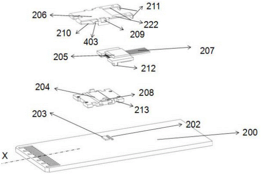
图2为本申请的光学引擎的第一实施方式的分解图。FIG. 2 is an exploded view of the first embodiment of the optical engine of the present application.
图3为光学引擎的第一实施方式的横截面图。3 is a cross-sectional view of a first embodiment of an optical engine.
图4为光学引擎的第一实施方式的侧视图。FIG. 4 is a side view of the first embodiment of the optical engine.
图5为光学引擎的第一实施方式的组装图。FIG. 5 is an assembly diagram of the first embodiment of the optical engine.
图6为跨接透镜组的透视图。FIG. 6 is a perspective view of a bridge lens group.
图7为跨接透镜组的仰视图。FIG. 7 is a bottom view of the bridge lens group.
图8为器件透镜组的俯视图。FIG. 8 is a top view of the device lens group.
图9为器件透镜组的仰视图。FIG. 9 is a bottom view of the device lens group.
图10为光学引擎的第二实施方式的分解图。Figure 10 is an exploded view of a second embodiment of an optical engine.
图11为光学引擎的第二实施方式的组装图。FIG. 11 is an assembly diagram of the second embodiment of the optical engine.
图12为光学引擎的第三实施方式的分解图。12 is an exploded view of a third embodiment of an optical engine.
图13为光学引擎的第三实施方式的组装图。FIG. 13 is an assembly diagram of a third embodiment of the optical engine.
图14为光学引擎的第三实施方式的横截面图。14 is a cross-sectional view of a third embodiment of an optical engine.
具体实施方式Detailed ways
现在将详细地阐述用于数据通信的光学引擎的优选实施方式,在下面的描述中还提供了用于数据通信的光学引擎的示例。虽然详细地描述了用于数据通信的光学引擎的示例性实施方式,但是对于相关技术领域中的技术人员来说很明显的是,对于理解用于数据通信的光学引擎而言不是非常重要的一些特征为了清楚起见并未显示。Preferred embodiments of optical engines for data communications will now be described in detail, and examples of optical engines for data communications are also provided in the description below. While exemplary embodiments of optical engines for data communications are described in detail, it will be apparent to those skilled in the relevant art that some of the optical engines for data communications are not critical to understanding Features are not shown for clarity.
此外,在本领域的普通技术人员阅读本说明书、附图和所附的权利要求书之后,对于本领域的普通技术人员来说显而易见的改进和修改被视为落入本申请的精神和保护范围内。In addition, after those of ordinary skill in the art have read the specification, the drawings and the appended claims, improvements and modifications obvious to those of ordinary skill in the art are deemed to fall within the spirit and protection scope of the present application Inside.
为了说明目的,下面出现的诸如“上”,“下”,“竖直”,“水平”,“顶部”和“底部”这些术语如在附图中所定向的,和本发明有关。应该理解,除非另有明确说明,本发明可以采用不同的位置。For descriptive purposes, terms such as "upper," "lower," "vertical," "horizontal," "top," and "bottom" appearing below are as oriented in the accompanying drawings in relation to the present invention. It should be understood that the present invention may take different positions unless expressly stated otherwise.
需要注意的是,在整个说明书和权利要求书中,当提到一个元件与另一个元件“联接”或“连接”时,不一定意味着一个元件紧固、固定、或附接到另一个元件。相反,术语“联接”或“连接”的意思是一个元件与另一个元件直接或间接连接,或者是机械的、电气的或光学通信的与另一个元件连接。It should be noted that throughout the specification and claims, when an element is referred to as being "coupled" or "connected" to another element, it does not necessarily mean that one element is fastened, fixed, or attached to the other element . In contrast, the terms "coupled" or "connected" mean that one element is directly or indirectly connected to another element, or in mechanical, electrical or optical communication with another element.
如本文中所使用的,“一个”指至少一个,除非另有明确指示。As used herein, "a" refers to at least one unless expressly indicated otherwise.
图1为现有技术的光学引擎。光学半导体器件的阵列101和器件驱动集成电路(IC)102布置在光电(OE)透镜组(block)103的腔中。跨接透镜和光纤阵列105与OE透镜组103光学地联接。该光学引擎对跨接透镜的对准精度具有很高的要求。但不仅真实透镜到垂直腔面发射激光器(VCSEL)/光电二极管(PD)的对准难以测量,而且这些具有多个透镜和内部全反射(TIR)表面的复杂透镜组还难以生产。在该光学引擎中,光纤走向无法灵活改变。此外,优化的发射器Tx和接收器Rx需要不同的透镜组。FIG. 1 is a prior art optical engine. An
图2至图5示出了本申请的用于数据通信的光学引擎的第一实施方式的不同视图。用于数据通信的光学引擎可以包括设定纵轴线X的电路基板200。光学半导体器件的阵列202可以横向地安装在基板200上。光学半导体器件的阵列可以与驱动集成电路(IC)203连接。光学半导体器件的阵列202可以是用于发送光学信号的发射型光电组件的阵列(诸如VCSEL阵列)、或用于接收光学信号的接收型光电组件的阵列(诸如光电二极管阵列)、或用于发送和接收光学信号的发射型光电组件和接收型光电组件的组合的阵列。Figures 2 to 5 show different views of the first embodiment of the optical engine for data communication of the present application. The optical engine for data communication may include a
器件透镜组204可以安装在基板200上且形成腔体221,该腔体221用于容纳光学半导体器件的阵列202,如图3所示。The
跨接透镜组205可以在器件透镜组204的上表面处与器件透镜组204联接。光纤阵列207可以安装在跨接透镜组205上且与光学半导体器件的阵列202光学地联接。The
如图2、图3和图4所示,跨接透镜组205可以形成有两个对准柱212,这两个对准柱212配置成与两个对准凹槽213紧密地接合或插入到两个对准凹槽213中,这两个对准凹槽213形成在器件透镜组204的两个相对侧上。对准柱212可以一体地形成在跨接透镜组205的底部表面上。对准柱212可以达致跨接透镜组205与器件透镜组204的精确的光对准。尽管已经示出和描述了跨接透镜组205设置有可插入到形成在器件透镜组204上的两个对准凹槽213中的两个对准柱212,但是应当理解,可以使用其它可行的对准方法。例如,器件透镜组204可以设置有可插入到形成在跨接透镜组205上的两个对准凹槽中的两个对准柱。跨接透镜组205和器件透镜组204也可以形成有其它对准部或结构,诸如销和销孔、突出部和凹口等。As shown in FIGS. 2 , 3 and 4 , the spanning
可以设置金属锁(latch)206以将跨接透镜组205固定在相对于器件透镜组204特定的位置上。金属锁206可以包括:两个锁槽209,这两个锁槽209形成在金属锁206的中间部分处的两个相对侧上,用于与两个锁勾208接合,这两个锁勾208形成在器件透镜组204上的中间部分处;以及两个柔性臂222,这两个柔性臂222从器件透镜组204中间部分的第一端处开始纵向延伸。至少一个突出部223可以形成在每个柔性臂222的底部表面上,用于与跨接透镜组205接触并按压其在器件透镜组204上。两个内弯端部211可以形成在两个柔性臂222的自由端上,用于紧靠跨接透镜组205的端部表面,以防止跨接透镜组205倾斜。两个U形弹簧210可以从器件透镜组204中间部分的第二端处开始延伸,用于接触并使器件透镜组204偏向基板200。一对突出部403可以分别从一对锁槽209开始纵向延伸,以在解锁时促进金属锁206脱离器件透镜组204。A
在本实施方式中,光纤阵列207可以平行于基板200布置在V形槽701内部。跨接透镜组205可以包括内部全反射表面224,该内部全反射表面224用于在接收光学信号时将来自光纤阵列207的光反射到光学半导体器件的阵列202的接收型光电组件,以及在发送光学信号时将来自光学半导体器件的阵列202的发射型光电组件的光反射到光纤阵列207。In this embodiment, the
图6和图7示出了跨接透镜组205的不同视图。跨接透镜组205可以形成有两个对准柱212,这两个对准柱212配置成插入到两个对准凹槽213中,这两个对准凹槽213形成在器件透镜组204的两个相对侧上,如图8和图9所示。对准柱212可以一体地形成在跨接透镜组205的底部表面上。对准柱212可以形成跨接透镜组205与器件透镜组204的精确的光对准。椭圆形透镜阵列603可以形成在跨接透镜组205的内部全反射表面224上。内部全反射表面224可以布置为相对于基板200成45度角。FIGS. 6 and 7 show different views of the
图8和图9示出了器件透镜组204的不同视图。可以看出,两个器件透镜阵列302可以分别形成在器件透镜组204的两个相对侧上。一个器件透镜阵列302可以用于发送光学信号,另一个器件透镜阵列302可以用于接收光学信号。两对对准凹槽213可以分别形成在器件透镜组204的两个相对侧上。每对对准凹槽213可以用于在其中容纳一个跨接透镜组205的一对对准柱212。FIGS. 8 and 9 show different views of the
用于数据通信的光学引擎的基础实施方式可以在四路小型可插拔(QSFP)板中采用12个通道。透镜光学器件可以仅附接在光学引擎的一侧上。不同功能区中的透镜可以供应不同的光学系统。跨接透镜组可以被插入光学引擎的两侧中以形成两个不同的光学耦合系统,例如一个光学耦合系统用于发射器Tx,一个光学耦合系统用于接收器Rx。两个透镜阵列(均用于发射器Tx和接收器Rx)可以被模塑在一片透镜组上。因此,本申请中公开的光学引擎的应用是灵活的。A basic implementation of an optical engine for data communications can employ 12 lanes in a quad small form-factor pluggable (QSFP) board. The lens optics may be attached on only one side of the optical engine. Lenses in different functional areas can supply different optical systems. Jumper lens sets can be inserted into both sides of the optical engine to form two different optical coupling systems, eg one optical coupling system for the transmitter Tx and one optical coupling system for the receiver Rx. Two lens arrays (both for transmitter Tx and receiver Rx) can be molded on one lens set. Therefore, the application of the optical engine disclosed in this application is flexible.
图10和图11示出了光学引擎的第二实施方式的不同视图。根据本实施方式,可以具有:两个横向的光学半导体器件的阵列1103、1104,这两个光学半导体器件的阵列1103、1104布置成并列排列且与两个并排式器件透镜组1101、1102光学地关联;以及两个并排式光纤阵列207,这两个光纤阵列207分别安装在两个并排式跨接透镜组205上且与两个光学半导体器件阵列1103、1104光学地联接。透镜阵列603可以形成在每个器件透镜组1101、1102上,用于分别耦合两个并列排列的光学半导体器件阵列1103、1104与设置在两个并排式跨接透镜组205上的两个光纤阵列207之间的光。两个金属锁206可以被设置用于分别将两个跨接透镜组205固定在相对于两个器件透镜组1101、1102特定的位置上。两个光学半导体器件的阵列1103、1104可以分别与两个驱动集成电路1105、1106连接。Figures 10 and 11 show different views of a second embodiment of the optical engine. According to this embodiment, it is possible to have two
两组12个通道可以被应用于发送或接收光学信号。该光学引擎设计可以与当前的QSFP印刷电路板兼容。如果需要,则可以扩展到多于两组12个通道。如果应用多组12个通道,则发送速度将超过300G且高达NX300G。Two sets of 12 channels can be used to transmit or receive optical signals. The optical engine design is compatible with current QSFP printed circuit boards. If desired, it can be expanded to more than two sets of 12 channels. If multiple groups of 12 channels are applied, the transmission speed will exceed 300G and up to NX300G.
图12至图14示出了光学引擎的第三实施方式的不同视图。根据本实施方式,可以具有:两个光学半导体器件的阵列1103、1104,这两个光学半导体器件的阵列1103、1104垂直于基板200的纵轴线X、沿着器件透镜组1201的腔1221的两个相对侧横向延伸;以及两个首尾相连的光纤阵列207,这两个光纤阵列207分别安装在两个首尾相连的跨接透镜组205上且与两个光学半导体器件的阵列1103、1104光学地联接。两个光学半导体器件的阵列1103、1104可以分别与两个驱动集成电路1105、1106连接。两个透镜阵列1110、1112可以形成在器件透镜组204上,用于分别耦合两个光学半导体器件的阵列1103、1104与设置在两个首尾相连的跨接透镜组205上的两个首尾相连的光纤阵列207之间的光。Figures 12 to 14 show different views of a third embodiment of the optical engine. According to this embodiment, there may be two
金属锁1202可以用于将两个跨接透镜组205固定在器件透镜组1201上的特定位置上。金属锁1202可以包括:两个锁槽209,这两个锁槽209形成在金属锁1202的中间部分处的两个相对侧上,用于与两个锁勾208接合,这两个锁勾208形成在器件透镜组1201上的中间部分处;以及第一对柔性臂1203和第二对柔性臂1204,第一对柔性臂1203从中间部分的第一端处开始纵向延伸,第二对柔性臂1204从中间部分的第二端处开始纵向延伸,用于分别接触两个跨接线透镜组205并将其按压在器件透镜组1201上。
光应答机可以设置有本申请中所公开的用于数据通信的光学引擎。可以在光应答机上应用两组12个通道。发射器Tx和接收器Rx可以共同被组装在单片上。通过使用多片,可以实现快速的数据发送/接收。这也可以帮助增大传输距离。The optical transponder may be provided with the optical engine disclosed in this application for data communication. Two sets of 12 channels can be applied on the optical transponder. The transmitter Tx and receiver Rx can be assembled together on a single chip. By using multiple slices, fast data transmission/reception can be achieved. This can also help increase the transmission distance.
光收发机也可以设置有本申请中所公开的用于数据通信的光学引擎。一个光学半导体器件的阵列202可以是用于发送光学信号的发射型光电组件的阵列,另一个光学半导体器件的阵列202可以是用于接收光学信号的接收型光电组件的阵列。Optical transceivers may also be provided with the optical engines disclosed in this application for data communication. One
尽管通过特别地参考多个优选实施方式已经示出并且描述了用于数据通信的光学引擎,应当注意的是,在不偏离所附的权利要求书的范围的情况下可以进行各种其它改变或修改。While an optical engine for data communication has been shown and described with particular reference to a number of preferred embodiments, it should be noted that various other changes or changes may be made without departing from the scope of the appended claims. Revise.
Claims (18)
Applications Claiming Priority (2)
| Application Number | Priority Date | Filing Date | Title |
|---|---|---|---|
| US14/933,010 US9606305B1 (en) | 2015-11-05 | 2015-11-05 | Optical engine for data communication |
| US14/933,010 | 2015-11-05 |
Publications (2)
| Publication Number | Publication Date |
|---|---|
| CN106918877A CN106918877A (en) | 2017-07-04 |
| CN106918877B true CN106918877B (en) | 2020-06-05 |
Family
ID=58360007
Family Applications (1)
| Application Number | Title | Priority Date | Filing Date |
|---|---|---|---|
| CN201610879292.XA Active CN106918877B (en) | 2015-11-05 | 2016-09-30 | Optical engine for data communication |
Country Status (2)
| Country | Link |
|---|---|
| US (1) | US9606305B1 (en) |
| CN (1) | CN106918877B (en) |
Families Citing this family (8)
| Publication number | Priority date | Publication date | Assignee | Title |
|---|---|---|---|---|
| US10168494B2 (en) * | 2016-11-30 | 2019-01-01 | International Business Machines Corporation | Off-axis micro-mirror arrays for optical coupling in polymer waveguides |
| US10914901B2 (en) * | 2017-10-17 | 2021-02-09 | International Business Machines Corporation | Lateral mounting of optoelectronic chips on organic substrate |
| CN108594375A (en) * | 2018-06-07 | 2018-09-28 | 深圳市极致兴通科技有限公司 | A kind of light path docking facilities of optical module |
| WO2021037085A1 (en) * | 2019-08-30 | 2021-03-04 | 青岛海信宽带多媒体技术有限公司 | Optical module |
| CN116325370A (en) * | 2020-10-13 | 2023-06-23 | 申泰公司 | Vertical plug-in interconnect system with ring connectors for high-speed data transmission |
| US11493707B2 (en) * | 2021-03-31 | 2022-11-08 | Enplas Corporation | Optical receptacle and optical module |
| CN114879324B (en) | 2022-06-24 | 2023-08-08 | 青岛海信宽带多媒体技术有限公司 | Optical module |
| CN114994839B (en) * | 2022-06-24 | 2023-08-08 | 青岛海信宽带多媒体技术有限公司 | Optical module |
Citations (3)
| Publication number | Priority date | Publication date | Assignee | Title |
|---|---|---|---|---|
| WO2012079448A1 (en) * | 2010-12-13 | 2012-06-21 | Sae Magnetics (H.K.) Ltd. | Electro-optical module and multi-functional latch member therefor |
| CN102866787A (en) * | 2011-07-07 | 2013-01-09 | 新科实业有限公司 | Side Mount Optical Navigation Module |
| US8469610B2 (en) * | 2011-01-18 | 2013-06-25 | Avago Technologies General Ip (Singapore) Pte. Ltd. | Optical connection system with plug having optical turn |
Family Cites Families (11)
| Publication number | Priority date | Publication date | Assignee | Title |
|---|---|---|---|---|
| JP2004246279A (en) * | 2003-02-17 | 2004-09-02 | Seiko Epson Corp | Optical module and manufacturing method thereof, optical communication device, opto-electric hybrid integrated circuit, circuit board, electronic equipment |
| JP2008225339A (en) * | 2007-03-15 | 2008-09-25 | Hitachi Cable Ltd | Optical system connection structure, optical member, and optical transmission module |
| JP2008257094A (en) * | 2007-04-09 | 2008-10-23 | Hitachi Cable Ltd | Optical transmission module and optical patch cable |
| US8335411B2 (en) * | 2008-11-11 | 2012-12-18 | Ultra Communications, Inc. | Fiber optic bi-directional coupling lens |
| JP5238651B2 (en) * | 2009-09-11 | 2013-07-17 | 株式会社フジクラ | Optical path changing member, optical connection method |
| JP5538108B2 (en) * | 2010-07-09 | 2014-07-02 | 株式会社エンプラス | Lens array and optical module having the same |
| JP5702596B2 (en) * | 2010-10-28 | 2015-04-15 | 株式会社エンプラス | Lens array and optical module having the same |
| WO2013077879A1 (en) * | 2011-11-23 | 2013-05-30 | Intel Corporation | Optical transceiver interface with c-shaped planar alignment and securing |
| WO2013077878A1 (en) * | 2011-11-23 | 2013-05-30 | Intel Corporation | Optical transceiver interface with planar alignment and securing |
| US20130216190A1 (en) * | 2012-02-20 | 2013-08-22 | Tyco Electronics Corporation | Optical assembly with ferrule and frame |
| JP6083401B2 (en) * | 2014-02-28 | 2017-02-22 | 株式会社村田製作所 | Manufacturing method of optical transmission module |
-
2015
- 2015-11-05 US US14/933,010 patent/US9606305B1/en active Active
-
2016
- 2016-09-30 CN CN201610879292.XA patent/CN106918877B/en active Active
Patent Citations (3)
| Publication number | Priority date | Publication date | Assignee | Title |
|---|---|---|---|---|
| WO2012079448A1 (en) * | 2010-12-13 | 2012-06-21 | Sae Magnetics (H.K.) Ltd. | Electro-optical module and multi-functional latch member therefor |
| US8469610B2 (en) * | 2011-01-18 | 2013-06-25 | Avago Technologies General Ip (Singapore) Pte. Ltd. | Optical connection system with plug having optical turn |
| CN102866787A (en) * | 2011-07-07 | 2013-01-09 | 新科实业有限公司 | Side Mount Optical Navigation Module |
Also Published As
| Publication number | Publication date |
|---|---|
| CN106918877A (en) | 2017-07-04 |
| US9606305B1 (en) | 2017-03-28 |
Similar Documents
| Publication | Publication Date | Title |
|---|---|---|
| CN106918877B (en) | Optical engine for data communication | |
| EP3596520B1 (en) | Assemblies of detachable optical connectors and optical chips | |
| CN211348752U (en) | Optical module | |
| US10270531B2 (en) | Optical transceiver and method of manufacturing the same | |
| US6739766B2 (en) | Lens array for use in parallel optics modules for fiber optics communications | |
| US9429725B2 (en) | Bidirectional parallel optical transceiver module and a method for bidirectionally communicating optical signals over an optical link | |
| US8961042B2 (en) | Optical coupling device | |
| US8412052B2 (en) | Surface mount (SMT) connector for VCSEL and photodiode arrays | |
| JP6127053B2 (en) | Multichannel transceiver | |
| CN108376847A (en) | Hybrid cable is to connector for substrate | |
| US7062132B2 (en) | Coupler assembly for an optical backplane system | |
| CN104272156B (en) | Apparatus, system and method for optically connecting a chipset to an optical connector | |
| JP2014115649A (en) | Optical communication module with fiber submount and latching optics assembly | |
| CN103003952B (en) | Optical communications module | |
| US8821040B2 (en) | Interposer | |
| US20130011103A1 (en) | Optoelectronic connector having improved optical module | |
| CN109477941B (en) | Silicon-based optical port providing passive alignment connectivity | |
| US9473239B2 (en) | Systems and methods for aligning an optical interface assembly with an integrated circuit | |
| US9025918B2 (en) | Photoelectric coupling module | |
| US8636426B2 (en) | Photoelectric conversion system with optical transceive module | |
| EP3757639B1 (en) | Optical subassembly with interposer | |
| US12204149B2 (en) | Interposer with feedback | |
| US20240313450A1 (en) | Daughter-card optical backplane connector system | |
| CN120813877A (en) | Optical back board connector system of sub-card | |
| WO2024189599A1 (en) | Daughter-card optical backplane connector system |
Legal Events
| Date | Code | Title | Description |
|---|---|---|---|
| PB01 | Publication | ||
| PB01 | Publication | ||
| SE01 | Entry into force of request for substantive examination | ||
| SE01 | Entry into force of request for substantive examination | ||
| TA01 | Transfer of patent application right | ||
| TA01 | Transfer of patent application right |
Effective date of registration: 20180829 Address after: 3 / F, new science centre, 6 science and technology Avenue East, Hongkong Science Park, Sha Tin, New Territories, Hongkong, China Applicant after: Yun Hui Technology Co., Ltd. Address before: Xinke center, 6 science and Technology Road East, Hongkong Science Park, Sha Tin, New Territories, Hongkong, China Applicant before: Xinke Industry Co., Ltd. |
|
| CB02 | Change of applicant information | ||
| CB02 | Change of applicant information |
Address after: Room 1515-1519, 15 / F, 19W building, 19 science and technology Avenue, Hong Kong Science Park, Pak Shek Kok, New Territories, Hong Kong, China Applicant after: SAE Magnetics (H.K.) Ltd. Address before: 3 / F, new science centre, 6 science and technology Avenue East, Hongkong Science Park, Sha Tin, New Territories, Hongkong, China Applicant before: SAE Magnetics (H.K.) Ltd. |
|
| GR01 | Patent grant | ||
| GR01 | Patent grant |