Disclosure of Invention
Embodiments of the present invention provide a system and a data processing method to improve efficiency and device utilization when data is transmitted between two data processing systems.
The embodiment of the invention provides a data processing system, which comprises a central processing unit CPU, a memory, a peripheral component interconnect express (PCIe) controller, a network adapter and at least one PCIe storage device, and is characterized by further comprising:
the management unit is used for acquiring a first storage address of requested data in the PCIe storage device according to first address information carried in a data request when the data processing system receives the data request, wherein the first storage address is a memory mapping input/output (MMIO) address;
the network adapter is used for directly reading data from the PCIe storage device according to the first storage address and transmitting the data to a second data processing system, or directly writing the data received from the second data processing system into the PCIe storage device, wherein the second data processing system is a data processing system which is communicated with the first data processing system through a network; the PCIe storage device comprises an address translation unit which is used for acquiring a second storage address of the data requested by the data request in the PCIe storage device according to the first storage address; the second storage address is a logical address that is linearly ordered with respect to non-linearly consecutive physical addresses.
Optionally, the second storage address is a physical address, and the physical address is a linear continuous address capable of directly reading data.
Optionally, the address translation unit is further configured to configure a first base address register BAR, where the first BAR address register stores a correspondence between the first storage address and the second storage address, and the second storage address is a linearly continuous storage address.
Optionally, the address translation unit is further configured to configure a second BAR address register, where the second BAR address register stores a correspondence between the first storage address and a virtual address of the second storage address, the second storage address is a non-linear continuous storage address, and the virtual address of the second storage address is an address obtained by linearly sorting the second storage address.
Optionally, the CPU allocates a unique identifier to each PCIe storage device, where the unique identifier is used to identify each PCIe storage device.
Optionally, the first address information includes a unique identifier of the PCIe storage device and a logical block address LBA.
Optionally, the management unit is further configured to establish a correspondence between the unique identifier and a base address in a BAR of the PCIe storage device.
The unique identification comprises at least one of a supplier identification code Vender ID, a Device identification code Device ID or a hard disk serial number; or the unique identification is obtained by performing hash processing on at least one of the sender ID, the Device ID or the hard disk serial number.
Optionally, the management unit includes a base address obtaining unit and a storage address obtaining unit:
the base address obtaining unit is configured to, when the data processing system receives a first data request of a second data processing system that communicates with the data processing system through a network, obtain a base address in a BAR of requested data according to a unique identifier of PCIe storage equipment that is carried in the first data request;
and the storage address acquisition unit is used for acquiring a first storage address of the requested data in the PCIe storage device according to the base address in the BAR and the LBA address carried by the first data request, wherein the first storage address is an MMIO address.
Optionally, the CPU registers the acquired first storage address in the network adapter.
Optionally, the data processing system further includes a sending unit, and the sending unit is configured to send the first storage address acquired by the management unit to the second data processing system.
Optionally, the PCIe controller obtains a data request that is sent by the network adapter and carries the first storage address, and the address translation unit obtains data of the second storage address, and returns the obtained data to the network adapter, or writes data sent by the network adapter into the second storage address.
Optionally, the management unit further includes a global base address obtaining unit and a global storage address obtaining unit:
the global base address obtaining unit is configured to, when the data processing system receives a second data request, obtain, according to a unique identifier of a PCIe storage device carried in the second data request, a base address of data requested by the second data request in a BAR of the second data processing system, where the second data request is a request to send data to the second data processing system or read data from the second data processing system;
the global storage address obtaining unit is configured to obtain, according to the base address in the BAR of the second data processing system and the LBA address carried in the second data request, an MMIO address of data requested by the second data request in the second data processing system.
Optionally, the data conversion unit in the PCIe controller of the second data processing system obtains a physical address or a logical address of the data requested by the second data request in the second data processing system according to the MMIO address of the data requested by the second data request sent by the data processing system in the second data processing system, where the physical address is a linear continuous address capable of directly reading data, and the logical address is an address obtained by linearly sequencing non-linear continuous physical addresses.
The embodiment of the invention also provides a method
The data processing method is applied to a data processing system comprising a Central Processing Unit (CPU), a memory, a peripheral component interconnect express (PCIe) controller, a network adapter and at least one PCIe storage device, and comprises the following steps:
when the data processing system receives a data request, acquiring first address information carried by the data request;
according to the first address information, a first storage address of the requested data in the PCIe storage device is obtained, wherein the first storage address is an MMIO address;
the network adapter reads data from the PCIe storage device directly according to the first storage address and transmits the data to the second data processing system, or writes the data received from the second data processing system into the PCIe storage device directly, wherein the second data processing system is a data processing system which communicates with the data processing system through a network; the PCIe storage device acquires a second storage address of the data requested by the data request in the PCIe storage device according to the first storage address; the second storage address is a logical address that is linearly ordered with respect to non-linearly consecutive physical addresses.
Optionally, the second storage address is a physical address, and the physical address is a linear continuous address capable of directly reading data.
Optionally, the method further includes:
the PCIe controller configures a first BAR address register that stores a correspondence between the first memory address and the second memory address, which is a linearly consecutive memory address.
Optionally, the method further includes:
the PCIe controller configures a second BAR address register, where the second BAR address register stores a corresponding relationship between the first storage address and a virtual address of the second storage address, the second storage address is a non-linear continuous storage address, and the virtual address of the second storage address is an address of the second storage address after linear ordering.
Optionally, the CPU allocates a unique identifier to each PCIe storage device, where the unique identifier is used to identify each PCIe storage device.
Optionally, the first address information includes a unique identifier of the PCIe storage device and a logical block address LBA.
Optionally, the method further includes:
and establishing a corresponding relation between the unique identification and a base address in the BAR of the PCIe storage device.
Optionally, the unique identifier includes at least one of a vendor identification code Vender ID, a Device identification code Device ID, or a hard disk serial number; or the unique identification is obtained by performing hash processing on at least one of the sender ID, the Device ID or the hard disk serial number.
Optionally, obtaining a first storage address of the requested data in the storage device includes:
acquiring a base address in a BAR of the requested data according to the unique identifier of the PCIe storage device carried in the first data request;
and acquiring a first storage address of the requested data in the PCIe storage device according to the base address in the BAR and the LBA address in the first data request, wherein the first storage address is an MMIO address.
Optionally, the CPU registers the acquired first storage address in the network adapter.
Optionally, the method further includes:
and the data processing system sends the acquired first storage address to the second data processing system.
Optionally, the PCIe controller obtains a data request carrying the first storage address sent by the network adapter, obtains data of a second storage address, and returns the obtained data to the network adapter, or writes data sent by the network adapter into the second storage address.
Optionally, the method further includes:
when the data processing system receives a second data request, according to the unique identifier of the PCIe storage device carried in the second data request, obtaining a base address of data requested by the second data request in a BAR of the second data processing system, where the second data request is used for sending data to the second data processing system or requesting to read data from the second data processing system;
and acquiring the MMIO address of the data requested by the second data request in the second data processing system according to the base address in the BAR of the second data processing system and the LBA address carried in the second data request.
Optionally, the PCIe controller in the second data processing system obtains a physical address or a logical address of the data requested by the second data request in the second data processing system according to the MMIO address of the data requested by the second data request sent by the data processing system in the second data processing system, where the physical address is a linear continuous address capable of directly reading data, and the logical address is an address obtained by linearly sequencing non-linear continuous physical addresses.
In the data processing system and the data processing method provided in the embodiments of the present invention, by obtaining the MMIO address of the data request, the MMIO address can directly obtain data stored in the PCIe storage device, and the network adapter can directly read data from the PCIe storage device of the data processing system and transmit the data to the second data processing system according to the MMIO address, or directly write data received from the second data processing system into the PCIe storage device. When the processing system is used for transmitting data between two data processing systems in network communication, the data transmission is directly transmitted from the PCIe storage device to the network adapter without passing through a memory. The occupancy rate of resources such as a memory, a CPU and the like when the two data processing system devices transmit data is reduced, and the data transmission efficiency is improved.
Detailed Description
The technical solutions in the embodiments of the present invention will be clearly and completely described below with reference to the drawings in the embodiments of the present invention, and it is obvious that the described embodiments are some, not all, embodiments of the present invention. All other embodiments, which can be obtained by a person skilled in the art without any inventive step based on the embodiments of the present invention, shall fall within the scope of protection of the present invention.
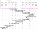
Fig. 1 is a schematic flowchart illustrating a process of moving data in a remote node storage device to a local node storage device in the prior art. Where a node may be a server or the like implementing the computing or storage functionality. When the Node1 needs to read the data stored in the storage device of Node2 from the Node2 through the network, the implementation process is as follows:
step 1, a CPU of a Node1 initiates a remote connection for requesting to read data;
step 2, the network adapter in Node1 sends the request message to the network adapter of the appointed Node (i.e. Node 2);
step 3, the network adapter of Node2 forwards the request message to the CPU of Node 2;
step 4, after the CPU of Node2 analyzes the request message, it sends a data request to the PCIe controller;
step 5, the PCIe controller reads the requested data to the memory in a DMA mode;
step 6, the CPU of Node2 sends the request data read to the memory to the network adapter;
step 7, the network adapter of Node2 sends the requested data to the network adaptation of Node1 through the network;
step 8, after the CPU of Node1 reads the requested data from its network adapter, it buffers the data to the memory;
step 9, the CPU of the Node1 sends the data cached in the memory to the PCIe controller to request to write the data into the storage device;
step 10, the PCIe controller of Node1 writes the received data into the storage device.
As can be seen from the process of data remote reading in the prior art, the CPU of the node participating in reading participates in data reading and writing, and each node needs to apply for a memory space to store data read by the CPU or to be written. Therefore, in the whole data transfer process, the time delay is inevitably increased due to more data transfer times, and the occupancy rates of the CPU and the memory are high.
In order to solve the problems of long-distance data migration delay and high CPU and memory occupancy rate in the prior art, the embodiment of the invention provides a data processing system, which aims to solve the problems of resource consumption and time delay caused by occupation of memory and CPU resources when data are read and written remotely between data processing systems in the prior art.
In order to solve the problems of more CPU (central processing unit) and memory resources and large transmission delay in cross-node data transmission in the prior art, the embodiment of the invention provides a data processing system, which combines a network technology and an MMIO (monolithic integrated peripheral component interconnect) address mapping technology of PCIe (peripheral component interconnect express) storage equipment, uses an inter-node data remote direct access technology to directly copy data, does not need a CPU (central processing unit) to participate in data movement in the copying process, only needs the CPU to control, and does not need to move the data to a memory in advance for processing, so that the utilization rates of the CPU and the memory are reduced; meanwhile, the migration process of data between the CPU and the memory is reduced, the time delay of data processing is reduced, and the efficiency of data transmission is improved.
Referring to fig. 2, fig. 2 is a schematic structural diagram of a data processing system 200 according to an embodiment of the present invention. The data processing system 200 includes a central processing unit CPU 202, a memory 206, a peripheral component interconnect express PCIe controller 203, a network adapter 205, and at least one PCIe storage device 204, and is characterized by further including:
a management unit 201, configured to, when the data processing system receives a data request, obtain a first storage address of the requested data in the storage device according to first address information carried in the data request, where the first storage address is an MMIO (Memory mapping I/O) address;
the network adapter 205 directly reads data from the PCIe memory device 204 according to the first memory address and transmits the data to a second data processing system, or directly writes data received from the second data processing system into the PCIe memory device 204, where the second data processing system is a data processing system that communicates with the first data processing system through a network.
The management unit 201 in the data processing system obtains the MMIO address of the data request, the MMIO address can directly obtain the data stored in the PCIe memory device, and the network adapter 205 can directly read the data from the PCIe memory device 204 of the data processing system 200 and transmit the data to the second data processing system according to the MMIO address, or directly write the data received from the second data processing system into the PCIe memory device 204; when the processing system is used for transmitting data between two data processing systems in network communication, the data transmission is directly transmitted from the PCIe storage device to the network adapter without passing through a memory. The occupancy rate of resources such as a memory, a CPU and the like when the two data processing system devices transmit data is reduced, and the data transmission efficiency is improved.
Referring to fig. 3, fig. 3 is a schematic diagram of an implementation of data processing system 200 according to an embodiment of the present invention. As shown in fig. 3, the PCIe memory device 203 further includes an address translation unit 2031, configured to obtain, according to the first memory address, a second memory address of the data requested by the data request in the PCIe memory device. The second storage address may be a physical address or a logical address, the physical address is a linear continuous address capable of directly reading data, and the logical address is an address obtained by linearly ordering a non-linear continuous physical address.
The address translation unit 2031 translates the first storage address, i.e. the MMIO address, into a second storage address, where the second storage address is a physical address of an accessible medium of the PCIe storage device 203, so that when the PCIe storage device receives a data request from the network adapter 205, the PCIe storage device can obtain a physical address of the accessible medium corresponding to the MMIO address according to the MMIO address carried in the data request, and read data through the physical address. When the accessible medium address in the PCIe storage device is not represented by an MMIO address, the network adapter can acquire the accessible medium address of the requested data, and direct reading and writing of the data are realized.
As an optional implementation manner, the address translation unit 2031 is further configured to configure a first base address register BAR (base address register), where the first BAR address register stores a correspondence between the first storage address and the second storage address, and the second storage address is a linearly continuous storage address. If the second storage address is a non-linear continuous storage address, the address translation unit is configured to configure a second BAR address register, where the second BAR address register stores a correspondence between the first storage address and a virtual address of the second storage address, and the virtual address of the second storage address is an address of the second storage address after linear ordering.
The BAR address register is configured by the address translation unit 2031, the linear continuous physical addresses in the PCIe memory device correspond to the MMIO addresses one to one, and the nonlinear continuous physical addresses in the PCIe memory device are linearly ordered to correspond to the MMIO addresses one to one, so that the mapping between the MMIO addresses and the accessible media addresses of the PCIe memory device is realized, the network adapter is mapped to the accessible storage media addresses one to one corresponding to the MMIO addresses by the PCIe controller according to the MMIO addresses, and the direct reading and writing of data are realized.
As an optional implementation manner, the CPU 202 allocates a unique identifier to each PCIe storage device, where the unique identifier is used to identify each storage device. Correspondingly, the management unit 201 is further configured to establish a correspondence between the unique identifier and a base address in a BAR of the PCIe storage device. Through the correspondence between the unique identifier of the PCIe storage device and the base address in the BAR of the PCIe storage device, the management unit 201 can obtain the base address in the BAR of the PCIe storage device corresponding to the unique identifier according to the unique identifier of the PCIe storage device included in the data request message received by the data processing system 200. Since the first Address information in the data request received by the data processing system includes a unique identifier and an LBA (Logical Block Address) Address of the PCIe storage device, the management unit 201 can obtain an MMIO Address of the requested data by obtaining the base Address and the LBA Address in the BAR of the PCIe storage device.
Optionally, the unique identifier includes at least one of a Vender ID, a Device ID, or a hard disk serial number; or the unique identification is obtained by performing hash processing on at least one of the sender ID, the Device ID or the hard disk serial number.
As an alternative implementation manner, as shown in fig. 3, the management unit 201 includes a base address obtaining unit 2011 and a storage address obtaining unit 2012:
the base address obtaining unit 2011 is configured to, when the data processing system 200 receives a first data request of a second data processing system that communicates with the data processing system over a network, obtain a base address in a BAR of requested data according to a unique identifier of the PCIe storage device 204 carried in the first data request;
a storage address obtaining unit 2012, configured to obtain, according to the base address in the BAR and the LBA address in the first data request, a first storage address of the requested data in the storage device, where the first storage address is an MMIO address.
As an optional implementation manner, the CPU 202 registers the acquired first storage address in the network adapter. The first storage address is registered in the network adapter, the network adapter 205 can issue the first storage address on the PCIe bus when receiving a data request carrying the first storage address by the second data processing system, and the PCIe controller 203 acquires the request and sends the requested data to the network adapter 205 when receiving the data request carrying the first storage address sent by the network adapter 205, or writes the data sent by the second data processing system and received by the network adapter into a position corresponding to the first storage address in the PCIe storage device.
As an optional implementation manner, the data processing system 200 further includes a sending unit 207, where the sending unit 207 is configured to send the first storage address acquired by the management unit 200 to the second data processing system.
Optionally, the PCIe controller 203 obtains a data request carrying the first storage address sent by the network adapter 205, and the address conversion unit 2031 obtains data of the second storage address, and returns the obtained data to the network adapter, or writes data sent by the network adapter into the second storage address.
In an embodiment of the present invention, the data processing system 200 communicates with another data processing system, such as a second data processing system, via a network to enable data to be transferred between the different data processing systems. The network includes, but is not limited to, ethernet, a transition cable technology IB network or an FC (fiber channel) network supporting multiple concurrent links, etc. The second data processing system may be a system implementing the solution described in the embodiment of the present invention, or may be a data processing system in the prior art. When the second data processing system is the system implementing the scheme of the embodiment of the invention, the second data processing system can also implement direct data reading or writing from or to the PCIe storage device by the network adapter.
As an optional implementation, the management unit 203 further includes a global base address obtaining unit 2033 and a global storage address obtaining unit 2034:
the global base address obtaining unit 2033 is configured to, when the data processing system receives a second data request, obtain, according to a unique identifier of a PCIe storage device carried in the second data request, a base address of data requested by the second data request in a BAR of the second data processing system, where the second data request is to send data to the second data processing system or read data from the second data processing system;
the global storage address obtaining unit 2034 is configured to obtain, according to the base address in the BAR of the second data processing system and the LBA address carried in the second data request, an MMIO address of the data requested by the second data request in the second data processing system.
Correspondingly, the data conversion unit in the PCIe controller of the second data processing system obtains a physical address or a logical address of the data requested by the second data request in the second data processing system according to the MMIO address of the data requested by the second data request sent by the data processing system in the second data processing system, where the physical address is a linear continuous address capable of directly reading data, and the logical address is an address obtained by linearly sequencing non-linear continuous physical addresses.
In the above embodiment, the management unit 203 further stores a corresponding relationship between the unique identifier of the PCIe storage device in the second data processing system and the base address in the BAR of the PCIe storage device, and when the data processing system 200 receives a second data request for sending data to the second data processing system or reading data from the second data processing system, the base address of the data requested by the second data request in the BAR of the second data processing system can be obtained, and the MMIO address of the data requested by the second data request is further obtained, so that direct transmission of data of the two data processing systems is realized, participation of a CPU and a memory is not required, resources of the CPU and the memory are saved, and efficiency of data transmission is improved. For example, the data transmission between the first data processing system and the second data processing system shown in fig. 8 is implemented, wherein the black dotted line part is the track and flow direction of the data transmission between the two data processing systems.
The data processing system 200 of the embodiment of the present invention may also be connected to a plurality of data processing systems via a communication network, and perform data transmission. The data processing system 200 may obtain the correspondence between the unique identifier of the PCIe storage device sent by the other data processing systems and the base address in the BAR of the PCIe storage device, so as to implement direct transmission between the data processing systems. The corresponding relation between the unique identification of the PCIe storage device and the base address in the BAR of the PCIe storage device can be requested from other data processing systems and stored, so that the direct transmission between the data processing systems can be realized. Of course, after the data processing system 200 obtains the corresponding relationship between the unique identifier of the PCIe storage device of the other data processing system and the base address in the BAR of the PCIe storage device, when the corresponding relationship between the unique identifier of the PCIe storage device of the other data processing system and the base address in the BAR of the PCIe storage device changes, the changed data processing system may send the changed corresponding relationship to the data processing system 200.
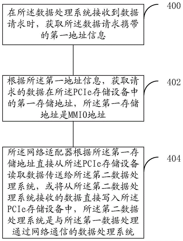
Referring to fig. 4, fig. 4 is a flowchart illustrating a data processing method according to an embodiment of the present invention. The data processing method of the embodiment of the invention is applied to a data processing system comprising a Central Processing Unit (CPU), a memory, a peripheral component interconnect express (PCIe) controller, a network adapter and at least one storage device, and is characterized by comprising the following steps:
step 400: when the data processing system receives a data request, acquiring first address information carried by the data request;
step 402: according to the first address information, a first storage address of the requested data in the PCIe storage device is obtained, wherein the first storage address is an MMIO address;
step 404: the network adapter reads data from the PCIe storage device directly according to the first storage address and transmits the data to the second data processing system, or writes the data received from the second data processing system into the PCIe storage device directly, wherein the second data processing system is a data processing system which communicates with the first data processing device through a network.
Step 400 and step 402 of the above method embodiment may be implemented by a management unit in the data processing system, where the management unit may be a module or a logic unit in the CPU, or may be a separate hardware entity in the data processing system.
The MMIO address of the data request is obtained through step 402 in the above embodiment, where the MMIO address can directly obtain data stored in PCIe storage device, and the network adapter can directly read data from the PCIe storage device of the data processing system and transmit the data to the second data processing system according to the MMIO address, or directly write data received from the second data processing system into the PCIe storage device; when the processing system is used for transmitting data between two data processing systems in network communication, the data transmission is directly transmitted from the PCIe storage device to the network adapter without passing through a memory. The occupancy rate of resources such as a memory, a CPU and the like when the two data processing system devices transmit data is reduced, and the data transmission efficiency is improved.
As an optional implementation manner, the data processing method further includes that the PCIe memory device obtains, according to the first memory address, a second memory address of the data requested by the data request in the PCIe memory device. The second storage address is a physical address or a logical address, the physical address is a linear continuous address capable of directly reading data, and the logical address is an address obtained by linearly ordering nonlinear continuous physical addresses.
Optionally, the PCIe controller configures a first BAR address register, where the first BAR address register stores a correspondence between the first storage address and the second storage address, and the second storage address is a linearly continuous storage address. Or the PCIe controller configures a second BAR address register, where the second BAR address register stores a correspondence between the first storage address and a virtual address of the second storage address, the second storage address is a non-linear continuous storage address, and the virtual address of the second storage address is an address obtained by linearly sorting the second storage address.
By configuring the BAR address register, the linear continuous physical addresses in the PCIe storage device correspond to the MMIO addresses one by one, and the nonlinear continuous physical addresses in the PCIe storage device correspond to the MMIO addresses one by one after linear sequencing, so that mapping between the MMIO addresses and the accessible medium addresses of the PCIe storage device is realized, the network adapter is mapped to the PCIe accessible storage medium addresses corresponding to the MMIO addresses one by one through the PCIe controller according to the MMIO addresses, and direct reading and writing of data are realized.
As an optional implementation manner, the data processing method further includes: and the CPU distributes a unique identifier for each PCIe storage device, wherein the unique identifier is used for identifying each PCIe storage device. And establishing a corresponding relation between the unique identifier and a base address in the BAR of the PCIe storage equipment according to the unique identifier.
Optionally, the first address information includes a unique identifier of the PCIe storage device and a logical block address LBA.
Optionally, the unique identifier includes at least one of a Vender ID, a Device ID, or a hard disk serial number; or the unique identification is obtained by performing hash processing on at least one of the sender ID, the Device ID or the hard disk serial number.
Through the corresponding relation between the unique identifier of the PCIe storage device and the base address in the BAR of the PCIe storage device, the base address in the BAR of the PCIe storage device corresponding to the unique identifier can be acquired according to the unique identifier of the PCIe storage device contained in the data request message received by the data processing system. Because the first address information in the data request received by the data processing system includes the unique identifier and the LBA address of the PCIe storage device, the MMIO address of the requested data can be acquired by acquiring the base address and the LBA address in the BAR of the PCIe storage device.
As an optional implementation manner, obtaining a first storage address of the requested data in the storage device includes:
acquiring a base address in a BAR of the requested data according to the unique identifier of the PCIe storage device carried in the first data request;
and acquiring a first storage address of the requested data in the PCIe storage device according to the base address in the BAR and the LBA address in the first data request, wherein the first storage address is an MMIO address.
Optionally, the CPU registers the acquired first storage address in the network adapter. And the data processing system sends the acquired first storage address to the second data processing system. When the network adapter of the data processing system receives a data request which is sent by the second data processing system and carries the first storage address, the network adapter issues the received data request on a PCIe bus, and the request can be received by a PCIe controller in the data processing system. And after the PCIe controller acquires a data request which is sent by the network adapter and carries the first storage address, acquiring a corresponding second storage address according to the first storage address, acquiring data from the second storage address, and returning the acquired data to the network adapter or writing the data sent by the network adapter into the second storage address.
As an optional implementation manner, the method further includes:
when the data processing system receives a second data request, according to the unique identifier of the PCIe storage device carried in the second data request, obtaining a base address of data requested by the second data request in a BAR of the second data processing system, wherein the second data request is used for sending data to the second data processing system or reading data from the second data processing system;
and acquiring the MMIO address of the data requested by the second data request in the second data processing system according to the base address in the BAR of the second data processing system and the LBA address carried in the second data request.
Correspondingly, the PCIe controller in the second data processing system obtains a physical address or a logical address of the data requested by the second data request in the second data processing system according to the MMIO address of the data requested by the second data request sent by the data processing system in the second data processing system, where the physical address is a linear continuous address capable of directly reading data, and the logical address is an address obtained by linearly sequencing non-linear continuous physical addresses.
By obtaining the corresponding relationship between the unique identifier of the PCIe memory device in the second data processing system and the base address in the BAR of the PCIe memory device, the base address of the data requested by the second data request in the BAR of the second data processing system can be obtained, and the MMIO address of the data requested by the second data request is further obtained, so that direct transmission of data of the two data processing systems is realized, involvement of a CPU and a memory is not required, resources of the CPU and the memory are saved, and the efficiency of data transmission is improved.
Fig. 5 schematically shows a basic hardware structure of an implementation of the data processing system according to an embodiment of the invention. The data processing system comprises basic hardware such as a CPU, a memory, a PCIe controller, a PCIe bus, a PCIe storage device, a network adapter and the like. The network adapter in the data processing system is a network adapter based on PCIe bus technology and supporting network Direct Access technology, wherein the network Direct Access technology includes but is not limited to RDMA (Remote Direct data Access) technology and the like; the network adapters include, but are not limited to, ethernet cards, IB HCAs (Infiniband Host Channel adapters, transition cable technology Host Channel adapters supporting multiple concurrent links), iWarp HCAs (internet wide area RDMA protocol Host Channel adapters supporting internet wide area RDMA protocol Host Channel adapters), Rapid IO HCAs (Rapid IO Host Channel adapters supporting fast reading and writing), and the like; the PCIe bus technology is used for indicating that the uplink bus interface of the network adapter is PCIe. The data processing system further comprises at least one PCIe storage device based on a PCIe bus, where the PCIe storage device includes, but is not limited to, a Memory, a hard Disk, an SSD (Solid State Disk), a Flash, an NVRAM (Non-Volatile Random Access Memory), and the like. Implementations of the data processing system include, but are not limited to, servers (rack, tower, frame, etc.), storage devices, or minicomputers.
In the data processing system of the embodiment of the present invention, on the basis of the hardware basic architecture shown in fig. 5, a management unit is added, where the management unit is configured to, when the data processing system receives a data request, obtain a first storage address of the requested data in the PCIe storage device according to first address information carried in the data request, where the first storage address is an MMIO address. The management unit may be implemented in a CPU, or may be implemented in separate hardware, and the embodiment of the present invention does not limit the implementation manner of the management unit in the data processing system.
Specifically, the management unit obtains the address of the data request received by the data processing system in the PCIe storage device through the established correspondence between the base address in the BAR of the PCIe storage device and the unique identifier of the PCIe storage device.
The Unique Identifier of the PCIe storage device, for example, a GUID (Globally Unique Identifier), is an Identifier that is uniquely determined for each PCIe storage device and allocated by the data processing system. The unique identifier may be a unique identifier assigned by the CPU, or may be a unique identifier assigned by the management unit. The unique identifier may be a unique group of character strings formed by a vendor ID (vendor identification code) of the PCIe storage Device, a Device ID (Device identification code), a unique tag ID (e.g., a hard disk serial number) of the storage Device attached to the PCIe storage Device, or an identifier obtained by hashing the character strings. The embodiment of the invention does not limit the composition of the unique identifier, as long as the information of the storage device in the node can be uniquely marked.
The base address in the BAR of the PCIe storage device is distributed when the data processing system is started, and after the data processing system is started, the management unit acquires the base address in the BAR of each PCIe storage device. The management unit may obtain the base address in the BAR of each PCIe storage device and the unique identifier of the PCIe storage device by scanning all PCIe storage devices in the data processing system.
And the management unit records the corresponding relation between the base address in the BAR of each PCIe storage device and the unique identifier of the PCIe storage device according to the acquired base address in the BAR of each PCIe storage device and the unique identifier of the PCIe storage device.
When the data processing system receives a data request, the data request carries a unique identifier and an LBA (Logical Block Address) Address of a PCIe storage device where requested data is located. The management unit acquires the base address of the requested data in the BAR of the PCIe storage device according to the unique identifier carried in the data request and the established corresponding relation between the base address in the BAR of each PCIe storage device and the unique identifier of the PCIe storage device; and obtaining the MMIO address of the requested data by combining the LBA address. The management unit may obtain the start address and the end address of the MMIO address of the requested data by:
start address ═ base address in mapped BAR + (LBA × block size)
End address ═ base address in the mapped BAR + ((LBA + number of blocks) × block size) -1.
The management unit is further configured to maintain a correspondence between the base address in the BAR of the PCIe storage device and the unique identifier of the PCIe storage device, and when the base address in the BAR of the PCIe storage device changes, refresh the correspondence between the base address in the BAR of the PCIe storage device and the unique identifier of the PCIe storage device. For example, the base address in the BAR of a PCIe storage device may change due to a reboot of the data processing system, i.e., the base address in the BAR of a PCIe storage device assigned by the data processing system for each PCIe storage device may be different from the last time. The management unit needs to refresh the corresponding relationship between the unique identifier of the PCIe storage device and the base address in the BAR of the PCIe storage device according to the unique identifier of each PCIe storage device.
The management unit can also acquire the corresponding relation between the base address in the BAR of the PCIe storage device and the unique identifier of the PCIe storage device in other data processing systems. Through the corresponding relation between the base address in the BAR of the PCIe storage device in the other data processing system and the unique identifier of the PCIe storage device, the storage address of the PCIe storage device in the other data processing system can be obtained when data is read and written for the other data processing system. The method comprises the steps of obtaining the corresponding relation between the base address in the BAR of the PCIe storage device in other data processing systems and the unique identification of the PCIe storage device, wherein the base address can be obtained by the data processing system by initiatively sending a request to other data processing systems, and the request can also be obtained by receiving the request sent by other data processing systems initiatively. The embodiment of the invention does not limit the specific acquisition mode.
Referring to fig. 6, fig. 6 is a diagram illustrating an exemplary correspondence relationship between the unique PCIe storage device identifier stored in the management unit and the base address in the BAR of the PCIe storage device according to the embodiment of the present invention. In the example diagram, the IP address is used to identify a unique address of the data processing system in the network where the data processing system is located, the GUID is a unique identifier of the PCIe storage device, and the mapping space start address is a start address of a mapping area of the PCIe storage device address in the CPU addressing space; the device logical address refers to a logical start address in the storage device; the spatial length refers to the entire length of the segment of the region mapped by the system.
In the embodiment of the present invention, the correspondence between the unique PCIe storage device identifier and the base address in the BAR of the PCIe storage device may be established by a driver of the PCIe storage device, or may be established by the management unit. Specifically, the loading may be performed automatically after the data processing system is started by adding a script, or may be performed manually. When the PCIe storage device is driven to be established, the PCIe BAR address register is firstly configured by the PCIe storage device, and the management unit reads the configured mapping relation. This is achieved by configuring the registers of the PCIe memory device when built by the management unit.
The PCIe storage device according to the embodiment of the present invention further includes an address translation unit, configured to obtain, according to the first storage address, a second storage address of the data requested by the data request in the PCIe storage device.
The address translation unit may be implemented in a PCIe device controller, to establish a corresponding relationship between a medium accessible address in the PCIe storage device and the MMIO address, and when a data read-write request for the MMIO address is received, may obtain, according to the MMIO address, a medium accessible address in the PCIe storage device corresponding to the MMIO address, for example, a storage address of the PCIe storage device, so as to perform data read-write.
Taking the PCIe storage device as the PCIe NVRAM as an example, according to the PCIe protocol specification it follows, the address space of the accessible medium inside the PCIe NVRAM is directly mapped to the MMIO address space of the CPU, so that all read and write requests to the PCIe NVRAM are equal to requests to the MMIO address. The MMIO address space corresponds to all accessible spaces of the NVRAM, namely, the corresponding relation between the media accessible address in the PCIe storage device and the MMIO address is established, and the corresponding NVRAM space can be directly accessed through the access of the MMIO address space. Directly mapping the address space of the accessible medium inside the PCIe NVRAM to the MMIO address space of the CPU may be implemented by configuring the BAR address register.
Fig. 7 is a schematic diagram illustrating a structural relationship for configuring mapping between internal addresses of PCIe memory devices and MMIO addresses of CPUs according to an embodiment of the present invention. The PCIe End Point in the PCIe controller in the figure is used as an address translation unit, configures a PCIe BAR address register, and maps addresses in the PCIe storage device to MMIO addresses of the CPU, so that accesses to a CPU address (address for DMA) space can be directly mapped to addresses of accessible media of the PCIe storage device.
In the embodiment of the invention, the corresponding relation between the medium accessible address in the PCIe storage device and the MMIO address is established, namely the mapping relation between the address space of the PCIe storage device and the MMIO address space in the CPU is established. The mapping relationship is established in different ways according to whether the physical address of the PCIe memory device is a linear continuous memory address.
When the physical addresses of the PCIe storage device are linearly continuous storage addresses, the BAR address register configured by the address translation unit maps a section of CPU address space with the size consistent with that of the actual storage device, and the addresses of the PCIe storage device correspond to the addresses of the mapped CPU address space one by one because the addresses of the PCIe storage device are linearly continuous. The CPU's operations on this address space can be obtained by an address translation unit that translates the received request into the physical address of the actual PCIe storage device.
When the physical address of the PCIe storage device is not a linear continuous storage address, the address translation unit establishes mapping between the linearly ordered storage address and the address of the CPU. The BAR address register is configured to map a CPU address space consistent with the size of a virtual address, wherein the virtual address is the linearly ordered address of the nonlinear continuous storage address. For example, sectors, blocks or other minimum unit units may be labeled consecutively to form a "virtual" linear space, and then a mapping relationship with the CPU address space is established.
Through the corresponding relation between the base address in the BAR of the PCIe storage device and the unique identifier of the PCIe storage device, which is established by a management unit in the data processing system, the management unit can acquire the MMIO address of the data of the request of the data request received by the data processing system and initiate the data request to a PCIe controller according to the MMIO address; and an address translation unit in the PCIe controller acquires the media-accessible address, namely the actual physical address, of the requested data in the PCIe storage device according to the established corresponding relation between the media-accessible address in the PCIe storage device and the MMIO address, and the data can be directly read or written through the media-accessible address.
Correspondingly, the network adapter in the data processing system can directly read data from the PCIe storage device or write data into the PCIe storage device according to the MMIO address. The problems of consumption of memory and CPU resources and transmission delay caused by the fact that related data on PCIe storage equipment need to be read into a physical memory first and then transmitted to a remote data processing system through the physical memory in the prior art are solved.
The following describes in detail the implementation of the data processing system and the data processing method according to the embodiments of the present invention, taking as an example that the first data processing system needs to write data of 4Kbytes, including the offset address 0x1000 to 0x2000, of the PCIe SSD F into the position 0x3000 to 0x4000 of the PCIe SSD G of the second data processing system. The PCIe SSD is a specific implementation of a PCIe storage device. This embodiment takes as an example that the first data processing system not only creates the correspondence between the unique identifier of the PCIe SSD itself and the base address in the BAR of the PCIe SSD, but also obtains the correspondence between the unique identifier of the PCIe SSD in the second data processing system and the base address in the BAR of the PCIe SSD.
Step 500: the first data processing system acquires a base address in a BAR of the PCIe SSD;
the first data processing system obtains the base address in the PCIe BAR of the PCIe SSD F as 0xff 000000 through the corresponding relation between the unique identifier of the PCIe SSD in the management unit and the base address in the BAR of the PCIe SSD, and obtains an MMIO address corresponding to the offset address 0x1000, such as 0xff 001000; meanwhile, a base address 0xfe 000000 in a PCIe BAR of the PCIe SSD G is obtained, and an MMIO address corresponding to 0x 3000-0 x4000 of the offset address, such as 0xfe003000, is obtained.
Step 502: a network adapter of a first data processing system initiates a data write request;
the network adapter of the first data processing system initiates a data request to the PCIe SSD F device through the new MMIO address 0xff 001000 of PCIe SSD F, the internal PCIe interface of the PCIe SSD F device converts the MMIO address into an internally accessible storage medium address XXX, and the result of XXX is different according to different mapping unit implementations. The PCIe SSD F reads data corresponding to the address XXX of the storage medium, and sends the data to the network adapter through the PCIe bus after the data are read, and the CPU does not need to participate in the data transmission process in the whole process and does not need to occupy the memory.
Step 504: the network adapter of the second data processing system receives the data sent by the network adapter of the first data processing system and sends the data to PCIe SSD G;
the network adapter of the second data processing system initiates a write data request to the PCIe SSD G device through the new MMIO address 0xfe003000 of the PCIe SSD G, the PCIe interface of the PCIe SSD G device translates the MMIO address into an internally accessible storage media address YYY, and the result of this yy will be different depending on the implementation of the different mapping units. The PCIe SSD G writes the data transmitted by the network adapter into the address YYY of the storage medium, and the CPU does not need to participate in the data transmission process in the whole process and does not need to occupy the memory.
The PCIe SSD F device internal PCIe interface converts the MMIO address to the internally accessible storage media address XXX and the PCIe SSD G device PCIe interface converts the MMIO address to the internally accessible storage media address YYY, for the case where the second storage address is a line-sequential physical address. When the second storage address is a logical address, the internal PCIe interface of the PCIe SSD F device converts the MMIO address into the internally accessible storage medium address XXX, and further needs to convert the MMIO address into a non-linear continuous address, which is not described herein again.
And for the condition that the first data processing system does not acquire the corresponding relation between the unique identifier of the PCIe SSD in the second data processing system and the base address in the BAR of the PCIe SSD, the management unit of the second data processing system establishes the corresponding relation between the unique identifier of the PCIe SSD in the second data processing system and the base address in the BAR of the PCIe SSD, and when the network adapter of the second data processing system receives the data read-write request sent by the first data processing system, the base address in the BAR of the PCIe SSD to which data is to be written is acquired according to the corresponding relation between the unique identifier of the PCIe SSD in the second data processing system and the base address in the BAR of the PCIe SSD, and the base address is directly written into the corresponding PCIe SSD.
In the above embodiments of the present invention, the PCIe storage device is taken as an example to illustrate an implementation manner of directly reading or writing data when data is transferred between different data processing systems. For storage devices that pass through a memory interface, such as SCM (storage Class memory), RRAM (resistive Random Access memory), NVDIMM (Non-Volatile DIMMs), etc., it is also possible to perform direct read/write processing of data on SCM, RRAM, and NVDIMM by a management unit, referring to the implementation of the PCIe storage device. When the system is started, the storage device (NVDIMM \ RRAM \ SCM) registers the accessed space in the system during initialization, and the storage device can be accessed by accessing the registered address. Unlike the above embodiments, there is no need to map the address of the address accessible medium in the PCIe storage device with the MMIO address, and there is no need to perform address translation, but in order for other data processing systems on the network to obtain the address of the data to be accessed, it is necessary to obtain the address of the storage device (NVDIMM \ RRAM \ SCM) in the system and synchronize the other data processing systems.
Those of ordinary skill in the art will appreciate that the elements and algorithm steps of the examples described in connection with the embodiments disclosed herein may be embodied in electronic hardware, computer software, or combinations of both, and that the components and steps of the examples have been described in a functional general in the foregoing description for the purpose of illustrating clearly the interchangeability of hardware and software. Whether such functionality is implemented as hardware or software depends upon the particular application and design constraints imposed on the implementation. Skilled artisans may implement the described functionality in varying ways for each particular application, but such implementation decisions should not be interpreted as causing a departure from the scope of the present invention.
It is clear to those skilled in the art that, for convenience and brevity of description, the specific working processes of the above-described systems, apparatuses and units may refer to the corresponding processes in the foregoing method embodiments, and are not described herein again.
In the several embodiments provided in the present application, it should be understood that the disclosed system, apparatus and method may be implemented in other ways. For example, the above-described apparatus embodiments are merely illustrative, and for example, the division of the units is only one logical division, and other divisions may be realized in practice, for example, a plurality of units or components may be combined or integrated into another system, or some features may be omitted, or not executed. In addition, the shown or discussed mutual coupling or direct coupling or communication connection may be an indirect coupling or communication connection through some interfaces, devices or units, and may also be an electric, mechanical or other form of connection.
The units described as separate parts may or may not be physically separate, and parts displayed as units may or may not be physical units, may be located in one place, or may be distributed on a plurality of network units. Some or all of the units can be selected according to actual needs to achieve the purpose of the solution of the embodiment of the present invention.
In addition, functional units in the embodiments of the present invention may be integrated into one processing unit, or each unit may exist alone physically, or two or more units are integrated into one unit. The integrated unit can be realized in a form of hardware, and can also be realized in a form of a software functional unit.
The integrated unit, if implemented in the form of a software functional unit and sold or used as a stand-alone product, may be stored in a computer readable storage medium. Based on such understanding, the technical solution of the present invention essentially or partially contributes to the prior art, or all or part of the technical solution can be embodied in the form of a software product stored in a storage medium and including instructions for causing a computer device (which may be a personal computer, a server, or a network device) to execute all or part of the steps of the method according to the embodiments of the present invention. And the aforementioned storage medium includes: a U-disk, a removable hard disk, a Read-Only Memory (ROM), a Random Access Memory (RAM), a magnetic disk or an optical disk, and other various media capable of storing program codes.
While the invention has been described with reference to specific embodiments, the invention is not limited thereto, and various equivalent modifications and substitutions can be easily made by those skilled in the art within the technical scope of the invention. Therefore, the protection scope of the present invention shall be subject to the protection scope of the claims.