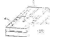
Figure 1A and 1B illustrate the cut-open view according to the structure of the magnetic head of a preferred embodiment of the present invention; Figure 1A is the cut-open view of coil pattern part, and Figure 1B then is the enlarged drawing of Ib part among Figure 1A;
Fig. 2 is for showing the completion amplification view of one deck copper plate on the medial end of coil pattern in the past;
Fig. 3 is for showing the amplification view of the copper plate of completion back on the medial end of coil pattern;
Fig. 4 for the copper plate on the medial end of showing coil pattern and on the amplification view of one deck gold film;
Fig. 5 forms the key diagram of the step of ridge on glassy layer for explanation;
Fig. 6 A, 6B and 6C illustrate the interval of the slot on the protective seam and are formed on relation between the shape of the ridge on the glassy layer; Fig. 6 A illustrates the big at interval situation of slot, and Fig. 6 B illustrates the little situation of slit separation, and Fig. 6 C illustrates the littler at interval situation of slot.
Fig. 7 is the planimetric map of a pair of half a head (head half);
Fig. 8 A and 8B illustrate the cross-section structure of a pair of half a head: Fig. 8 A is the cut-open view on the VIIIa-VIIIa line among Fig. 7, and Fig. 8 B is the cut-open view on the VIIIb-VIIIb line among Fig. 7;
Fig. 9 is used in the skeleton view of making a substrate in the half a head;
Figure 10 is the skeleton view that is illustrated in the first groove procedure of processing of carrying out on the substrate;
Figure 11 is the skeleton view of the formation step of displaying metal magnetic film;
Figure 12 is for showing the skeleton view of glass filling step;
Figure 13 is the skeleton view that is illustrated in second and the three-flute procedure of processing of carrying out on the substrate;
Figure 14 is for showing the skeleton view of glass filling step;
Figure 15 is the skeleton view that is illustrated in the 4th and the 5th groove procedure of processing of carrying out on the substrate;
Figure 16 is for showing the skeleton view of glass filling and screed step;
Figure 17 is the enlarged drawing of the XV II part (a undressed intact half a head) among Figure 16;
Figure 18 A is the planimetric map of the undressed intact half a head of Figure 17, and Figure 18 B then is its cut-open view;
Figure 19 A is the planimetric map that glassy layer is provided with the undressed intact half a head of photoresist, and Figure 19 B then is its cut-open view;
Figure 20 A is the planimetric map that has the undressed intact half a head of recessed portion in glassy layer, and Figure 20 B then is its cut-open view;
Figure 21 A is the planimetric map that is provided with the undressed intact half a head of copper facing basement membrane, and Figure 21 B then is its cut-open view;
Figure 22 A is the planimetric map that basement membrane is provided with the undressed intact half a head of photoresist, and Figure 22 B then is its cut-open view;
Figure 23 A is the planimetric map that is provided with the undressed intact half a head of copper plating film, and Figure 23 B then is its skeleton view;
Figure 24 A is for going up the planimetric map that the basement membrane that does not have copper plate forms the undressed intact half a head of a coil pattern by removing thereon, and Figure 24 B then is its cut-open view;
Figure 25 A is the planimetric map that the uncompleted half a head of one deck photoresist is set on copper plate, and Figure 25 B then is its cut-open view;
Figure 26 A is for having removed the planimetric map of the later uncompleted half a head of unnecessary copper plate part, and Figure 26 B then is its cut-open view;
Figure 27 A is the planimetric map that is provided with the uncompleted half a head of one deck insulating protective film in recessed portion, and Figure 27 B then is its cut-open view;
Figure 28 A is the planimetric map of the uncompleted half a head behind its surface evening, and Figure 28 B then is its cut-open view;
Figure 29 A is the planimetric map that has formed the uncompleted half a head of one deck gold film in its surface, and Figure 29 B then is its cut-open view;
Figure 30 A is the planimetric map that forms the uncompleted half a head of one deck photoresist on golden film, and Figure 30 B then is its cut-open view;
Figure 31 A is the planimetric map that golden film has constituted the uncompleted half a head behind the pattern, and Figure 31 B then is its cut-open view;
Figure 32 is for showing the skeleton view of a pair of uncompleted half a head along the line of its cutting;
The skeleton view of Figure 33 for showing how a pair of half a head is fixed together;
Figure 34 A is the skeleton view of a pair of half a head that is fixed together, and Figure 34 B then is their cut-open view;
Figure 35 is for removing the skeleton view of the magnetic head of unnecessary part;
Figure 36 is the planimetric map according to a pair of half a head of another preferred embodiment;
Figure 37 is the cut-open view along the E-E line among Figure 36;
Figure 38 is the cut-open view according to a pair of half a head that has been fixed together of another preferred embodiment that is similar to Figure 37; And
Figure 39 is the cut-open view according to a pair of half a head that has been fixed together of another preferred embodiment that is similar to Figure 37.
A preferred embodiment of the present invention is described with reference to the accompanying drawings.
The magnetic head of this preferred embodiment is to be fixed together by a pair of half a head that a substrate with each spiral coil pattern that forms thereon with the film forming method constitutes to make.Fig. 7 is the amplification view of these half a heads, and Fig. 8 A is the cut-open view along VIIIa-VIIIa line among Fig. 7, and Fig. 8 B then is the cut-open view along VIIIb-VIIIb line among Fig. 7.This magnetic head by a half a head 9 shown in arrow among the figure, be fixed on basically with an identical shaped half a head 39 of this half a head 9 on constitute.
Half a head 9 has following structure: a recessed portion 10 is provided on the surface of one deck glass 4 on the ceramic substrate 1, and forms a coil pattern 11 with the film forming method on the 10a of the bottom surface of recessed portion 10.A part is arranged near the medial end 11a of coil pattern 11, wherein not recessed, and the metal magnetic membrane portions 3 of formation post gap 3b is exposed on the surface of glass 4.This metal magnetic film 3 is that this end of substrate forms a part that constitutes anterior diastema 3a being imbedded in from formation post gap 3b to the glass 4 of substrate one end.
Terminal portion 12 extends to the other end of substrate 1 from the outboard end of coil pattern 11, and another terminal portion 13 that leaves coil pattern 11 is provided with abreast with terminal portion 12.Metal magnetic film 3 is formed on the skewed surface of a groove that is provided with on the substrate, and this groove is discussed later.
Golden film 14 is bonded in the outside on glass of recessed portion 10, a golden film 15 is on the post gap part 3b of metal magnetic film 3, a golden film 16 is on the medial end 11a of coil pattern 11, a golden film 17 is on the part of the terminal portion 12 of connecting coil pattern 11, and a golden film 18 is on the medial end of terminal portion 13.With one deck insulating protective film 23 topped coil pattern 11 of inserting in the recessed portion 10.The medial end 11a of coil pattern is exposed on the surface of insulating protective film 23, and golden film 16 is to be bonded on the medial end 11a of this exposure.
Half a head 39 terminal portions 12 are provided with coupling part 42 and 43 (being shorter than terminal portion 12 and 13) with 13 position and are used to be connected terminal portion 12 and 13, and half a head 39 is shorter than half a head 9.The remainder of half a head 39 has and half a head 9 identical construction.The parts that constitute half a head 39 are used on the reference number of corresponding component of half a head 9 and add that 30 reference numbers that obtain illustrate.
Be appreciated that when half a head 9 and 39 is fixed together that from Fig. 7 and Fig. 8 metal magnetic film 3 and 33 forms closed magnetic circuit, and golden film 14 and anterior diastema of 44 formation, golden film 15 and 45 then forms a post gap.Coil pattern 11 and 41 is connected to each other by golden film 16 and 46 and constitutes a single coil.
Arrive terminal portion 13 by the golden film on electric current flowing through coil pattern 11, golden film 16 and 46, coil pattern 41 and the coupling part 42 of terminal portion 12 inputs 47.Electric current also flows through on opposite direction.Gold film 17 there is no need for being electrically connected of coil pattern with 48, but the instability when preventing that half a head 9 and 39 is fixed together is helpful.
The place that should note in this preferred embodiment is to be provided with little ridge in glassy layer 4 and 34 on the position of the medial end 11a of coil pattern 11 and 41 and 41a.This point describes in detail with reference to Fig. 1 to Fig. 6.
Figure 1A is and the corresponding amplification view of Fig. 8 B of a magnetic head that comprises a pair of half a head that is fixed together that Figure 1B then is the zoomed-in view of the part Ib shown in the with dashed lines among Figure 1A.
Coil pattern 11 is formed in the recessed portion 10 in the glassy layer 4 of half a head 9, and coil pattern 11 is topped with one deck insulating protective film 23 except its medial end 11a.On the position of a plurality of ridge 4a with triangular-section and width W 1 with the medial end 11a place that is formed on coil pattern 11 on the glassy layer 4 apart from one another by d.
Coil pattern 11 comprises with plating mode and is plated in copper coating 19 on the basement membrane 20 that comprises aluminium oxide, chromium and copper and form by this order lamination.The copper coating 19a of the medial end 11a of coil pattern 11 has the shape of the ridge protuberance that constitutes along with a plurality of ridge 4a that are formed in the glassy layer 4.Insulating protective film 23 is in the recessed portion that is filled between these ridges.
Gold film 16 is bonded on the copper coating 19a, and the golden film 16 of topped width W 2 contacts on copper coating 19a and the lip-deep a plurality of position thereon.Because on the medial end 11a of coil pattern 11, copper coating 19a is formed in carinate lip-deep that ridge 4a by glassy layer 4 constitutes, and the upper surface 19b of the copper coating 19a in this district is all the other spiral parts that are higher than copper coating 19.
As mentioned above, half a head 9 is fixed on another half a head 39 and constitutes magnetic head, and the parts that constitute half a head 39 are by add that 30 reference numbers that draw illustrate in the drawings on the reference number of the corresponding component of half a head 9.By when being pressed together, half a head 9 and 39 being heated to 200 to 400 ℃ and they are fixed together.
With this method, as long as simply the medial end 11a of coil pattern 11 and 41 and 41a are made than the remainder height of coil pattern, just can guarantee between coil pattern 11 and 41 medial end 11a and the 41a by golden film 16 and 46 be electrically connected, and its reliability is high.
If the width W 1 of ridge 4a in the glassy layer and 34a and interval d are all less than 1 μ m, then ridge is too meticulous and be difficult to raise fully coil pattern medial end 11a and 41a, and when they during all above 10 μ m, then ridge seems very little and to contact the zone (integral multiple of width W 2) of golden film 16 and 46 too little; Under above two kinds of situations, electrical connection is unsafty.Make angle θ that the bottom surface 10a of the inclined-plane 4b of ridge and recessed portion 10 constitutes greater than 30 ° and be very suitable for producing above-mentioned effect less than 90 °.
A kind of method that forms the ridge of triangular-section in glassy layer is described below.
When forming ridge when the pattern of the photoresist on the glassy layer being made crack with seam and by ion-milling, ideally, the wall (as shown in Figure 5) that is substantially perpendicular to the first type surface of glassy layer 4,34 will be formed on the below, slit of photoresist.Yet in fact this does not occur, but forms the wall on slope, and what obtain is the ridge of pedestal shape, as shown in Fig. 6 A.When the distance between the lacquer crack in the photoresist diminished, ridge became the narrow pedestal shown in Fig. 6 B, becomes the triangular-section shown in Fig. 6 C then.
As shown in Figure 2, when forming copper coating 19 and 49 on basement membrane 20 and 50, copper coating 19 and 49 is taked the shape according to the carinate surface of ridge 4a and 34a formation.Then insulating protective film 23 and 53 is filled into the recessed portion of copper coating 19 and 49, and the leveling surface, as shown in Figure 3.Then, be bonded in golden film 16 and 46 on copper coating 19 and 49 and make pattern, as shown in Figure 4.No matter the degree of depth of surface cutting is much in above-mentioned surface evening technology, always there is copper coating to exist from the teeth outwards.This is that copper coating is formed on the inclined-plane of ridge 4a because in electroplating technology.
With this method, on the medial end of coil pattern, it is the same that copper coating forms as if piles up.In addition, this technology only comprises above-mentioned simple operations.
The manufacturing process of the magnetic head of this preferred embodiment is described below.
At first, as shown in Figure 9, preparation one flat plate shape substrate 1.Substrate 1 can be by making such as magnetic materials such as iron, but from for example prevent hyperchannel using cross (talk) and reduce on the viewpoint of impedance of magnetic head, the most handy such as the such nonmagnetic substance of potassium titanate.
Certainly not only above-mentioned potassium titanate also can use other various nonmagnetic substances; Comprising calcium titanate, barium titanate, zirconia (zirconium oxygen), aluminium oxide, aluminium-titanium carbonate, SiO, MnO-NiO mixed sintering material, zinc ferrite, crystallized glass and high rigidity glass.
Then, as shown in Figure 10, on the first type surface 1a of substrate 1, carry out the first groove processing technology.Carry out this groove processing technology and be for the metal magnetic film that in step after a while, forms can be at an angle with respect to the first type surface 1a (this is that magnetic gap forms the surface) of substrate 1.Thereby first groove 2 is to form with predetermined inclined-plane 2a on depth direction.
Finish after the above-mentioned groove processing, comprising that groove 2 (and especially on above-mentioned inclined-plane 2a) forms metal magnetic film 3 on the entire main surface 1a of interior substrate 1, as shown in Figure 11.Form technology such as various films such as vacuum coating or spraying plating and can be used as the method that forms metal magnetic film 3.
Any material with high saturation magnetic flux metric density and good soft magnetism feature all can be used for metal magnetic film 3, comprising crystalline alloy such as Fe-Al-Si alloy (especially sendust), Fe-Al alloy, Fe-Si-Co alloy, Fe-Ga-Si alloy, Fe-Ga-Si-Ru alloy, Fe-Al-Ga alloy, Fe-Ga-Ge alloy, Fe-Si-Ge alloy, Fe-Co-Si-Sl alloy and Fe-Ni alloy etc.
As an alternative, also can use amorphous alloy such as one or more the illustrated metal of alloy-metalloid amorphous alloy among one or more and element P, C, B, the Si among containing element Fe, Co, the Ni, perhaps have these elements as principal ingredient and comprise the alloy of Al, Ge, Be, Sn, In, Mo, W, Ti, Mn, Cr, Zr, Hf or Nb and have rare earth element and transition metal such as Co, Hf, Zr as the metal-metal amorphous alloy of their principal ingredient.
Then, in glass 4 being filled into first groove 2 that is formed on the substrate 1 and after flattening the surface, as shown in Figure 12, with second groove 5 and the three-flute 6 of cutting technique formation, as shown in Figure 13 with first groove, 2 quadratures.
Second groove 5 is corresponding to the coil groove of common block magnetic head, and forms for the front side degree of depth and the rear side degree of depth of the metal magnetic film 3 of setting previous formation and magnetic circuit that metal magnetic film 3 is constituted become a closed loop.Three-flute 6 becomes unwanted metal magnetic film 3 after for the final assembling of erasing head and is provided with.
Then, as shown in Figure 14, glass 4 is filled in second groove 5 and the three-flute 6, and first type surface 1a is flattened.
Then, as shown in Figure 15, form four groove 7 and five groove 8 parallel with first groove 2 with cutting technique.Here, the 4th groove 7 forms they and an edge joint that is formed on the metal magnetic film 3 on the groove inclined-plane 2a is touched, and control metal magnetic film 3 in abutting connection with width, i.e. road width.The 5th groove 8 is to be provided with for unnecessary metal magnetic film 3 that removing is positioned on the bottom surface of groove 2.
Then, as shown in Figure 16, glass 4 is filled in the 4th groove 7 and the 5th groove 8, and the leveling surface.
Form the magnetic circuit part that constitutes by metal magnetic film 3 with above-mentioned steps.Figure 17 illustrates and takes out from Figure 16 and (the observing from different perspectives) and a corresponding part of an independent magnetic head (part XV II shown in broken lines) of amplifying.The method that forms a coil in Figure 17 among the district XVIII that is shown in broken lines is described below.
Figure 18 is the same with Figure 17, on the substrate 1 corresponding to the enlarged drawing of the part of an independent magnetic head; Figure 18 A is a planimetric map of showing the further amplification of the rectangle region XVIII that is shown in broken lines among Figure 17, and Figure 18 B then shows along the section of the dotted line among Figure 18 A (also being like this in following figure).
As shown in Figure 18 A, metal magnetic film 3 appears at magnetic gap and forms on the surface on the position of two separation; The center part is post gap part 3b, then is anterior diastema part 3a with groove 5 and the part that this post gap part 3b separates.Two parts are oblique being formed on the substrate 1 as shown in Figure 18 B all.Post gap part 3b is that the glass 4 that is filled in each groove surrounds.
On this glassy layer 4, form suitable with the profile of a coil haply protective seam 61, as shown in Figure 19 with photoetching process.At this moment, on protective seam 61 parts, have many slot 61a corresponding to the coil pattern medial end.
Then, as shown in Figure 20, carry out selective etch with ion-milling and form the recessed portion corresponding 10, and wash photoresist 60 off with the profile of coil.
Here, be glass 4 owing to institute in above-mentioned ion-milling is etched, so recessed portion 10 is to form with good precision.And, the ridge 4a of formation triangular-section between the slot 61a in above-mentioned protective seam.Various substrates are illustrated in the following table through the degree of depth of the recessed portion that obtained behind the ion-milling in two hours and the smart rugosity of basal surface of recessed portion.As an alternative, can provide a plurality of minor diameter open-works to replace slot in the protective seam.The ridge of triangular-section will be an island shape in this case.
Table substrate degree of depth roughness TiO-CaO 2.0 μ m 50nm monocrystalline ferrous acid MnZn 2.2 μ m 20nm (Monocrystalline MnZn Ferrite) SiO-PbO-BO glass 4.3 μ m 10nm
As can be seen from the above table,, form the recessed portion 10 of coiler part more deeply, preferably adopt glass for good precision.
Except above-mentioned ion-milling, also can use chemical erosion, active-ion-etch, powder beam erosion (powder beam etching) etc. as the method that forms recessed portion 10.Because these method physics or chemically disconnect the atom of etched part, therefore when etched part was polycrystal, difference just was difficult to form a smooth recessed portion 10 to the ratio of the atom of disconnection along with the crystal grain difference; Yet, if material is such as amorphous materials such as glass, just might form smooth recessed portion 10.Be difficult to form space (recessed portion) with machining in required part.
Then, as shown in Figure 21, on whole surface, form the basement membrane of the substrate of the copper coating that constitutes coil pattern by spraying plating.Basement membrane 20 is to make by the order that forms one deck pellumina (0.2 μ m is thick), one deck chromium film (0.01 μ m is thick) and one deck copper film (0.2 μ m is thick), but not shown in the drawings this hierarchy.
Apply a kind of photoresist then, and make the pattern shown in Figure 22 according to the coil pattern that will form.In Figure 22, the photoresist behind the pattern is made in reference number 62 expressions.
Then, make with photoresist 62 to carry out copper facing, form the copper coating 19 that a layer thickness is approximately 3.5 μ m whereby, and photoresist 62 is washed off, as shown in Figure 23 as mask.
Then, as shown in Figure 24, remove the basic unit 20 that does not have copper coating 19 in the above, thereby finished coil pattern 11 with ion-milling.At this moment, copper coating 19 plays mask.
Then, as shown in Figure 25, apply one deck photoresist 63, and be made into pattern and it is stayed on the zone of not wanting to etch away.
Then substrate is immersed in the ferric chloride solution, remove unnecessary copper with chemical etching whereby, and stay the coil pattern 11 that comprises copper coating 19.Can adopt ion-milling, active-ion-etch or powder beam etching and so on to replace chemical erosion to carry out the removing of the unnecessary part of copper coating.
Then, apply a kind of insulation protection material, and be made into pattern as shown in Figure 27 like that, thereby it is retained in the recessed portion 10, whereby, coil pattern 11 is subjected to the protection of insulating protective film 23.In this preferred embodiment, adopt one deck photoresist to be hardened and become insulating protective film 23 as the insulation protection material and by being heated to 200 to 400 ℃.
Use the polishing and leveling surface then, and as shown in Figure 28, be exposed to the copper coating on the medial end 11a of coil pattern 11 whereby.
Then, be formed for constituting the nonmagnetic film 74 of magnetic gap by spraying plating to half thickness of gap length, as shown in Figure 29.This nonmagnetic film 74 is that the order by titanium, gold is formed into the gross thickness of 0.1 μ m.
Be applied to one deck photoresist on the nonmagnetic film 74 then and make pattern, photoresist 64 is stayed on the post gap part 3b of the medial end 11a of coil pattern 11, metal magnetic film 3 and the LHA of recessed portion 10 (forming the part of anterior diastema), as shown in Figure 30.
64 carry out ion-milling with photoresist then, remove the unnecessary part of golden film (nonmagnetic film) whereby as mask.With this method, as shown in Figure 31, stay the golden film 14 (comprise anterior diastema and form the district) on the zone in the outside of recessed portion 10, post gap forms the golden film 15 on the part, golden film 16 on the medial end 11a of coil pattern 11, golden film 17 on the terminal portion 12 and the golden film 18 on the terminal portion 13.
Then, as shown in Figure 32, difference A-A along the line, B-B and C-C, D-D cuts out half a head of making 9 and the half a head made from identical technology 39 in said method.This cutting as above face is mentioned with reference to Fig. 7, and the coupling part 42 and 43 of half a head 39 is shorter than the terminal portion 12 and 13 of half a head 9.
The half a head 9 and 39 that then will be cut into the preliminary dimension among Figure 32 is fixed together as shown in Figure 33 like that, makes the uncompleted magnetic head shown in Figure 34 whereby.Figure 34 A is the skeleton view of uncompleted magnetic head, and Figure 34 B is then for passing through the cut-open view on the line of coil medial end 11a.Said fixing, such as in early time description, on 250 to 300 ℃, undertaken by hot pressing.
Cut away the unnecessary lateral section of uncompleted magnetic head then, and obtain the magnetic head shown in Figure 35 whereby.
In the description of the step shown in Figure 18 to Figure 34, a single half a head has been discussed; Above-mentioned technology is to carry out on a plate-like workpieces that comprises a plurality of half a heads shown in the set of diagrams 16, and finally obtains single uncompleted half a head by cutting this workpiece but in fact.
As mentioned above, in a magnetic head according to present embodiment since the medial end of coil pattern be formed in the glassy layer by ridge form carinate lip-deep, this end is the remainder that is higher than coil pattern.As a result, this medial end to coil pattern just can easily and link together reliably, and has guaranteed high productivity and high reliability.
And in this magnetic head, because the recessed portion of the corresponding shape of shape of formation and coil pattern around post gap, and coil pattern is formed in this recessed portion, on the surface that magnetic recording media just slides thereon, do not form unnecessary opening (hole), unnecessaryly fill any this opening yet with glass.As a result, eliminated breaking and short circuit of the film coil pattern that causes by filling glass.
And in this magnetic head manufacturing process,, therefore guaranteed good gap precision owing to be the leveling of carrying out abutment surface (being that magnetic gap forms the surface) after in the recessed portion that forms in advance, forming coil pattern again with ion-milling.
Except photoresist, also can adopt such as the material of the stable insulating material of these classes of nitride such as oxides such as glass, aluminium oxide and monox, silicon nitride as insulating protective film.When adopting one of them,, flatten its surface then by the thickness formation skim of spraying plating to 6 to 8 μ m.
In an example as a comparison, done following change: in the step of the formation recessed portion of in above-mentioned preferred embodiment, describing, form the degree of depth with ion-milling and be approximately the recessed portion of 4.5 μ m and slot is not set in protective seam with reference to Figure 19 and Figure 20; In above-mentioned preferred embodiment, in the step of the formation copper coating of describing with reference to Figure 23, copper coating is formed the thickness of about 5 μ m; In the step of the pattern of in above-mentioned preferred embodiment, describing of making golden film, removed unnecessary portions (the thick part of 0.5 to 1 μ m of upper section that comprises the coil pattern of insulating protective film and medial end) with reference to Figure 31.
In this example, removed the insulating protective film on the coil pattern and made it not existed.Therefore, need some other steps to come to make the be electrically connected medial end of continuous part of coil pattern and another coil pattern with the topped again coil pattern of one deck insulating protective film and the formation that raises.
In above-mentioned preferred embodiment, on two substrates, all form the film coil pattern; Yet, also can only a coil pattern be set on a substrate, and an interconnector is set on another piece substrate.This is that the medial end that is arranged on the coil pattern on this substrate is to be electrically connected with an interconnector that is arranged on another piece substrate with a terminal portion (terminal portion be not connected on the coil pattern on this piece substrate).
Figure 36 is for showing the planimetric map similar to Fig. 7 of the half a head that constitutes with this method, and Figure 38 and Figure 39 are that two half a heads are fixed together afterwards along the cut-open view of the E-E line of Figure 36.
In the example of Figure 37, the half a head 9 that is used in the above-mentioned preferred embodiment is as one of half a head, then is used as another half a head with the half a head shown in the reference number 101.
In half a head 101, electroplate by 103 inside of the recessed portion in glassy layer 102 a L shaped copper interconnector 104 is set, with golden film 105 and 106 it is connected to the golden film 16 and 18 of half a head 9, and terminal portion 13 is connected to the medial end 11a of coil pattern 11 by interconnector 104.Topped one deck insulating protective film 108 on interconnector 104.In Figure 37, golden film of reference number 107 expressions, it constitutes a magnetic gap with golden film 14.
In the example in Figure 38, be used in half a head 9 in the above-mentioned preferred embodiment and be as one of half a head, and in order to a half a head shown in the reference number 111 as another half a head and without the half a head in the example shown in Figure 37 101.
In half a head 111, recessed portion is not set in glassy layer 112, do not have golden film on the copper interconnector 114 on the glassy layer 112 but directly with half a head 9 on golden film 16 link to each other with 18.In Figure 38, reference number 114a represents to be used for constituting with golden film 14 copper substrate of a magnetic gap.In addition, this example is identical with the example shown in Figure 37.
In the example shown in Figure 39, be the half a head 9 and 101 that is used for replacing among Figure 37 with the half a head shown in reference number 131 and 121.
On the glassy layer 132 of half a head 131, any ridge is not set, the surface of coil pattern 141 is made flat, and on coil pattern 141 not topped insulating protective film 153.
In the glassy layer 122 of half a head 121, recessed portion 123 is set, and in glassy layer, on the position in the face of the terminal portion 148 of the coupling part of the medial end 141a of coil pattern 141 and half a head 131, forms ridge 122a and 122b respectively.The result is just protruded outside the copper back panel wiring in the part of these locational copper back panel wirings 124 on the glassy layer 122, and the golden film 125 that is arranged in here links to each other with terminal portion 148 with coil pattern medial end 141a respectively with 126.
Example has following advantage among Figure 36 to 39, and when the minority number of turn in the film coil was just enough, the structure of one of half a head can be simplified.
Described a preferred embodiment of the present invention above, but on the basis of technological concept of the present invention, can make various corrections this preferred embodiment.
For example, the ingredient that suitable material beyond above-mentioned and shape can be used as magnetic head.And except the magnetic head of VCR, the present invention also can be applied on the magnetic head of audio frequency and other purposes.
In the present invention, on the substrate position owing to the electrical connections that is present in the film coil between a pair of substrate in correspondence, formed the surface on a plurality of and the surperficial oblique direction that forms film coil, just on the carinate surface that forms by these inclined-planes, formed film coil or be connected electrical connections on the film coil.
As a result, because the surface of electrical connections is higher than other current-carrying part, and exists a conductive layer forever on the surface after the processing, thereby to be electrically connected be firm, and there is not short circuit in the place beyond electrical connections, and reliability is high.
The surface that there is no need to use any independent step to make electrical connections raises, and manufacturing is simple.