CN107123721B - A kind of encapsulation structure and encapsulation method of LED with lens - Google Patents
A kind of encapsulation structure and encapsulation method of LED with lens Download PDFInfo
- Publication number
- CN107123721B CN107123721B CN201710544822.XA CN201710544822A CN107123721B CN 107123721 B CN107123721 B CN 107123721B CN 201710544822 A CN201710544822 A CN 201710544822A CN 107123721 B CN107123721 B CN 107123721B
- Authority
- CN
- China
- Prior art keywords
- metal layer
- lens
- flip
- cavity
- chip
- Prior art date
- Legal status (The legal status is an assumption and is not a legal conclusion. Google has not performed a legal analysis and makes no representation as to the accuracy of the status listed.)
- Active
Links
- 238000000034 method Methods 0.000 title claims abstract description 15
- 238000005538 encapsulation Methods 0.000 title description 11
- 229910052751 metal Inorganic materials 0.000 claims abstract description 90
- 239000002184 metal Substances 0.000 claims abstract description 90
- 238000004806 packaging method and process Methods 0.000 claims abstract description 35
- 239000010410 layer Substances 0.000 claims description 113
- 239000003292 glue Substances 0.000 claims description 22
- 239000011229 interlayer Substances 0.000 claims description 14
- 239000000853 adhesive Substances 0.000 claims description 8
- 230000001070 adhesive effect Effects 0.000 claims description 8
- VYPSYNLAJGMNEJ-UHFFFAOYSA-N Silicium dioxide Chemical compound O=[Si]=O VYPSYNLAJGMNEJ-UHFFFAOYSA-N 0.000 claims description 7
- 239000000843 powder Substances 0.000 claims description 7
- 239000000741 silica gel Substances 0.000 claims description 7
- 229910002027 silica gel Inorganic materials 0.000 claims description 7
- PNEYBMLMFCGWSK-UHFFFAOYSA-N Alumina Chemical compound [O-2].[O-2].[O-2].[Al+3].[Al+3] PNEYBMLMFCGWSK-UHFFFAOYSA-N 0.000 claims description 3
- 238000009713 electroplating Methods 0.000 claims description 3
- 238000001755 magnetron sputter deposition Methods 0.000 claims description 3
- OGIDPMRJRNCKJF-UHFFFAOYSA-N titanium oxide Inorganic materials [Ti]=O OGIDPMRJRNCKJF-UHFFFAOYSA-N 0.000 claims description 3
- GWEVSGVZZGPLCZ-UHFFFAOYSA-N Titan oxide Chemical compound O=[Ti]=O GWEVSGVZZGPLCZ-UHFFFAOYSA-N 0.000 claims 1
- 238000007747 plating Methods 0.000 claims 1
- 238000005476 soldering Methods 0.000 abstract 1
- OAICVXFJPJFONN-UHFFFAOYSA-N Phosphorus Chemical compound [P] OAICVXFJPJFONN-UHFFFAOYSA-N 0.000 description 19
- 239000000084 colloidal system Substances 0.000 description 4
- 238000010586 diagram Methods 0.000 description 4
- 230000017525 heat dissipation Effects 0.000 description 4
- 230000000694 effects Effects 0.000 description 3
- 239000000758 substrate Substances 0.000 description 3
- PXHVJJICTQNCMI-UHFFFAOYSA-N Nickel Chemical compound [Ni] PXHVJJICTQNCMI-UHFFFAOYSA-N 0.000 description 2
- 150000002739 metals Chemical class 0.000 description 2
- 238000007740 vapor deposition Methods 0.000 description 2
- RYGMFSIKBFXOCR-UHFFFAOYSA-N Copper Chemical compound [Cu] RYGMFSIKBFXOCR-UHFFFAOYSA-N 0.000 description 1
- BQCADISMDOOEFD-UHFFFAOYSA-N Silver Chemical compound [Ag] BQCADISMDOOEFD-UHFFFAOYSA-N 0.000 description 1
- 239000002313 adhesive film Substances 0.000 description 1
- 229910045601 alloy Inorganic materials 0.000 description 1
- 239000000956 alloy Substances 0.000 description 1
- 230000009286 beneficial effect Effects 0.000 description 1
- 238000002507 cathodic stripping potentiometry Methods 0.000 description 1
- 239000011248 coating agent Substances 0.000 description 1
- 238000000576 coating method Methods 0.000 description 1
- 229910052802 copper Inorganic materials 0.000 description 1
- 239000010949 copper Substances 0.000 description 1
- PCHJSUWPFVWCPO-UHFFFAOYSA-N gold Chemical compound [Au] PCHJSUWPFVWCPO-UHFFFAOYSA-N 0.000 description 1
- 229910052737 gold Inorganic materials 0.000 description 1
- 239000010931 gold Substances 0.000 description 1
- 239000000463 material Substances 0.000 description 1
- 238000000465 moulding Methods 0.000 description 1
- 229910052759 nickel Inorganic materials 0.000 description 1
- 230000005693 optoelectronics Effects 0.000 description 1
- 239000011241 protective layer Substances 0.000 description 1
- 238000009877 rendering Methods 0.000 description 1
- 239000011347 resin Substances 0.000 description 1
- 229920005989 resin Polymers 0.000 description 1
- 229910052709 silver Inorganic materials 0.000 description 1
- 239000004332 silver Substances 0.000 description 1
- 238000005507 spraying Methods 0.000 description 1
- 238000003466 welding Methods 0.000 description 1
Images


Classifications
-
- H—ELECTRICITY
- H10—SEMICONDUCTOR DEVICES; ELECTRIC SOLID-STATE DEVICES NOT OTHERWISE PROVIDED FOR
- H10H—INORGANIC LIGHT-EMITTING SEMICONDUCTOR DEVICES HAVING POTENTIAL BARRIERS
- H10H20/00—Individual inorganic light-emitting semiconductor devices having potential barriers, e.g. light-emitting diodes [LED]
- H10H20/80—Constructional details
- H10H20/85—Packages
- H10H20/8506—Containers
-
- H—ELECTRICITY
- H10—SEMICONDUCTOR DEVICES; ELECTRIC SOLID-STATE DEVICES NOT OTHERWISE PROVIDED FOR
- H10H—INORGANIC LIGHT-EMITTING SEMICONDUCTOR DEVICES HAVING POTENTIAL BARRIERS
- H10H20/00—Individual inorganic light-emitting semiconductor devices having potential barriers, e.g. light-emitting diodes [LED]
- H10H20/80—Constructional details
- H10H20/85—Packages
- H10H20/851—Wavelength conversion means
- H10H20/8515—Wavelength conversion means not being in contact with the bodies
-
- H—ELECTRICITY
- H10—SEMICONDUCTOR DEVICES; ELECTRIC SOLID-STATE DEVICES NOT OTHERWISE PROVIDED FOR
- H10H—INORGANIC LIGHT-EMITTING SEMICONDUCTOR DEVICES HAVING POTENTIAL BARRIERS
- H10H20/00—Individual inorganic light-emitting semiconductor devices having potential barriers, e.g. light-emitting diodes [LED]
- H10H20/80—Constructional details
- H10H20/85—Packages
- H10H20/855—Optical field-shaping means, e.g. lenses
-
- H—ELECTRICITY
- H10—SEMICONDUCTOR DEVICES; ELECTRIC SOLID-STATE DEVICES NOT OTHERWISE PROVIDED FOR
- H10H—INORGANIC LIGHT-EMITTING SEMICONDUCTOR DEVICES HAVING POTENTIAL BARRIERS
- H10H20/00—Individual inorganic light-emitting semiconductor devices having potential barriers, e.g. light-emitting diodes [LED]
- H10H20/80—Constructional details
- H10H20/85—Packages
- H10H20/857—Interconnections, e.g. lead-frames, bond wires or solder balls
-
- H—ELECTRICITY
- H10—SEMICONDUCTOR DEVICES; ELECTRIC SOLID-STATE DEVICES NOT OTHERWISE PROVIDED FOR
- H10H—INORGANIC LIGHT-EMITTING SEMICONDUCTOR DEVICES HAVING POTENTIAL BARRIERS
- H10H20/00—Individual inorganic light-emitting semiconductor devices having potential barriers, e.g. light-emitting diodes [LED]
- H10H20/80—Constructional details
- H10H20/85—Packages
- H10H20/858—Means for heat extraction or cooling
- H10H20/8581—Means for heat extraction or cooling characterised by their material
-
- H—ELECTRICITY
- H10—SEMICONDUCTOR DEVICES; ELECTRIC SOLID-STATE DEVICES NOT OTHERWISE PROVIDED FOR
- H10H—INORGANIC LIGHT-EMITTING SEMICONDUCTOR DEVICES HAVING POTENTIAL BARRIERS
- H10H20/00—Individual inorganic light-emitting semiconductor devices having potential barriers, e.g. light-emitting diodes [LED]
- H10H20/01—Manufacture or treatment
- H10H20/036—Manufacture or treatment of packages
-
- H—ELECTRICITY
- H10—SEMICONDUCTOR DEVICES; ELECTRIC SOLID-STATE DEVICES NOT OTHERWISE PROVIDED FOR
- H10H—INORGANIC LIGHT-EMITTING SEMICONDUCTOR DEVICES HAVING POTENTIAL BARRIERS
- H10H20/00—Individual inorganic light-emitting semiconductor devices having potential barriers, e.g. light-emitting diodes [LED]
- H10H20/01—Manufacture or treatment
- H10H20/036—Manufacture or treatment of packages
- H10H20/0361—Manufacture or treatment of packages of wavelength conversion means
-
- H—ELECTRICITY
- H10—SEMICONDUCTOR DEVICES; ELECTRIC SOLID-STATE DEVICES NOT OTHERWISE PROVIDED FOR
- H10H—INORGANIC LIGHT-EMITTING SEMICONDUCTOR DEVICES HAVING POTENTIAL BARRIERS
- H10H20/00—Individual inorganic light-emitting semiconductor devices having potential barriers, e.g. light-emitting diodes [LED]
- H10H20/01—Manufacture or treatment
- H10H20/036—Manufacture or treatment of packages
- H10H20/0363—Manufacture or treatment of packages of optical field-shaping means
-
- H—ELECTRICITY
- H10—SEMICONDUCTOR DEVICES; ELECTRIC SOLID-STATE DEVICES NOT OTHERWISE PROVIDED FOR
- H10H—INORGANIC LIGHT-EMITTING SEMICONDUCTOR DEVICES HAVING POTENTIAL BARRIERS
- H10H20/00—Individual inorganic light-emitting semiconductor devices having potential barriers, e.g. light-emitting diodes [LED]
- H10H20/01—Manufacture or treatment
- H10H20/036—Manufacture or treatment of packages
- H10H20/0364—Manufacture or treatment of packages of interconnections
Landscapes
- Led Device Packages (AREA)
Abstract
本发明涉及一种带透镜式LED封装结构及封装方法,该封装结构包括透镜和倒装LED芯片,所述透镜的入光面的中部具有一内凹的腔体,所述透镜的入光面上还设有位于腔体的周缘并且相互绝缘的第一金属层和第二金属层,所述倒装LED芯片安装在腔体内,并且该倒装LED芯片的两个电极裸露在腔体外,倒装LED芯片的两个电极分别与第一金属层和第二金属层相电连接,以解决现有CSP封装结构存在易损坏以及焊接困难的问题。
The invention relates to a lens-type LED packaging structure and packaging method. The packaging structure includes a lens and a flip-chip LED chip. The middle part of the light incident surface of the lens has a concave cavity. The light incident surface of the lens There are also a first metal layer and a second metal layer that are located on the periphery of the cavity and are insulated from each other. The flip-chip LED chip is installed in the cavity, and the two electrodes of the flip-chip LED chip are exposed outside the cavity. The two electrodes on which the LED chips are mounted are electrically connected to the first metal layer and the second metal layer respectively, so as to solve the problems of easy damage and difficult soldering in the existing CSP packaging structure.
Description
技术领域technical field
本发明涉及一种光电领域,具体是涉及一种带透镜式LED封装结构及封装方法。The invention relates to the field of optoelectronics, in particular to a lens-equipped LED packaging structure and packaging method.
背景技术Background technique
CSP(Chip Scale Package)封装,是芯片级封装的意思,特别是基于倒装芯片开发的CSP以其优异的出光效率、良好的散热结构、精巧的外形尺寸等优点,已开始应用于背光、闪光灯、商用照明等高端用途。CSP (Chip Scale Package) packaging means chip-level packaging, especially the CSP based on flip-chip development has begun to be used in backlights and flashlights due to its excellent light output efficiency, good heat dissipation structure, and compact dimensions. , commercial lighting and other high-end applications.
现有的CSP封装主要包括以下几种结构,结构A:荧光胶膜包覆倒装LED芯片形成5面出光CSP结构;结构B:由结构A变化而来,用白色反光硅胶做垂直墙面,形成单面发光结构;结构C:该结构应用无粘性的荧光胶片贴在具有白色反光杯的灌封LED封装体上,也是一种单面出光结构;结构D:运用喷涂荧光胶的方法在芯片上形成50-70微米的超薄荧光层,再用透明硅胶在反射杯内灌封保护。Existing CSP packages mainly include the following structures. Structure A: fluorescent adhesive film covers flip-chip LED chips to form a 5-sided light-emitting CSP structure; structure B: a change from structure A, using white reflective silica gel as the vertical wall, Form a single-sided light-emitting structure; structure C: this structure is pasted on the potted LED package with a white reflective cup with a non-adhesive fluorescent film, which is also a single-sided light-emitting structure; structure D: use the method of spraying fluorescent glue on the chip Form an ultra-thin fluorescent layer of 50-70 microns on the surface, and then use transparent silica gel to seal and protect the reflection cup.
以上几种CSP的封装结构核心特点是以封装树脂对倒装芯片做厚度约50-150um的五面包覆、仅裸露电极一面,形成单面或五面出光的封装结构,由于芯片上附着的封装层的厚度都很薄,以及硅胶和芯片之间的附着力比较差,而且硅胶也比较软,在这些CSP封装结构受到比较大的外力时,封装层会存在脱落的情况,造成这些封装结构失效。另外由于这些CSP封装结构的焊盘就是倒装芯片的电极,因此焊盘都很小,在直接焊接到基板上时存在对位不准、虚焊的问题。The core feature of the packaging structure of the above CSPs is that the packaging resin covers the flip chip on five sides with a thickness of about 50-150um, and only one side of the electrode is exposed to form a single-side or five-side light-emitting packaging structure. The thickness of the packaging layer is very thin, and the adhesion between the silica gel and the chip is relatively poor, and the silica gel is relatively soft. When these CSP packaging structures are subjected to relatively large external forces, the packaging layer will fall off, causing these packaging structures. invalidated. In addition, since the pads of these CSP packaging structures are the electrodes of the flip chip, the pads are very small, and there are problems of misalignment and virtual soldering when directly soldered to the substrate.
发明内容Contents of the invention
本发明旨在提供一种带透镜式LED封装结构及封装方法,以解决现有CSP封装结构存在易损坏以及焊接困难的问题。The present invention aims to provide a lensed LED packaging structure and packaging method to solve the problems of easy damage and difficult welding in the existing CSP packaging structure.
具体方案如下:The specific plan is as follows:
一种带透镜式LED封装结构,包括透镜和倒装LED芯片,所述透镜的入光面的中部具有一内凹的腔体,所述透镜的入光面上还设有位于腔体的周缘并且相互绝缘的第一金属层和第二金属层,所述倒装LED芯片安装在腔体内,并且该倒装LED芯片的两个电极裸露在腔体外,倒装LED芯片的两个电极分别与第一金属层和第二金属层相电连接。A lens-type LED packaging structure, including a lens and a flip-chip LED chip, the middle of the light-incident surface of the lens has a concave cavity, and the light-incident surface of the lens is also provided with a And the first metal layer and the second metal layer are insulated from each other, the flip-chip LED chip is installed in the cavity, and the two electrodes of the flip-chip LED chip are exposed outside the cavity, and the two electrodes of the flip-chip LED chip are respectively connected to the The first metal layer and the second metal layer are electrically connected.
优选的,所述带透镜式LED封装结构还具有第三金属层和第四金属层,所述第三金属层覆盖在第一金属层以及与第一金属层相电连接的电极上,所述第四金属层覆盖在第二金属层以及与第二金属层相电连接的电极上,所述第三金属层和第四金属层之间相互绝缘。Preferably, the encapsulation structure of LED with lens also has a third metal layer and a fourth metal layer, the third metal layer covers the first metal layer and the electrodes electrically connected to the first metal layer, the The fourth metal layer covers the second metal layer and the electrodes electrically connected to the second metal layer, and the third metal layer and the fourth metal layer are insulated from each other.
优选的,所述第三金属层和第四金属层由磁控溅射、电镀或者蒸镀的方式形成。Preferably, the third metal layer and the fourth metal layer are formed by magnetron sputtering, electroplating or vapor deposition.
优选的,所述腔体内还具有透光的固晶胶,所述倒装LED芯片通过该固晶胶固定到透镜上。Preferably, there is also a light-transmitting die-bonding glue in the cavity, and the flip-chip LED chip is fixed on the lens through the die-bonding glue.
优选的,所述倒装LED芯片与腔体的内壁之间的间隙内填充有导热胶。Preferably, the gap between the flip-chip LED chip and the inner wall of the cavity is filled with thermal conductive glue.
优选的,所述导热胶由硅胶以及纳米氧化钛和/或纳米氧化铝制成。Preferably, the thermal conductive adhesive is made of silica gel, nano-titanium oxide and/or nano-alumina.
优选的,所述透镜的出光面上还设有荧光粉层。Preferably, a phosphor layer is further provided on the light-emitting surface of the lens.
优选的,所述透镜的入光面和出光面之间具有一夹层,所述夹层内填充有荧光粉层。Preferably, there is an interlayer between the light incident surface and the light exit surface of the lens, and the interlayer is filled with a phosphor layer.
本发明还提供了一种带透镜式LED封装结构的封装方法,包括以下步骤,The present invention also provides a method for encapsulating a lens-type LED encapsulation structure, comprising the following steps,
S1、提供透镜,所述透镜的入光面的中部具有一内凹的腔体,所述透镜的入光面上还设有位于腔体的周缘并且相互绝缘的第一金属层和第二金属层;S1. Provide a lens, the middle part of the light incident surface of the lens has a concave cavity, and the light incident surface of the lens is also provided with a first metal layer and a second metal layer located on the periphery of the cavity and insulated from each other layer;
S2、将具有凹腔的透镜倒置在平台上,使其凹腔朝上,在凹腔内点透光的固晶胶,以电极朝上的方式将倒装LED芯片放置在凹腔内;S2. Put the lens with concave cavity upside down on the platform so that the concave cavity faces upwards, place light-transmitting crystal-bonding glue in the concave cavity, and place the flip-chip LED chip in the concave cavity with the electrodes facing upwards;
S3、固化固晶胶,使倒装LED芯片固定在凹腔内;S3, solidifying the die-bonding glue, so that the flip-chip LED chip is fixed in the concave cavity;
S4、在倒装LED芯片和凹腔的间隙内填充导热胶;S4, filling the gap between the flip-chip LED chip and the concave cavity with thermal conductive glue;
S5、固化导热胶;S5, curing thermally conductive adhesive;
S6、形成金属层,金属层将倒装LED芯片的两个电极分别与透镜上的两个相互绝缘的金属层电连接起来。S6, forming a metal layer, the metal layer electrically connects the two electrodes of the flip-chip LED chip with the two mutually insulated metal layers on the lens respectively.
优选的,还包括以下步骤,Preferably, the following steps are also included,
S7、在透镜上形成荧光粉层;S7, forming a phosphor layer on the lens;
S8、固化荧光粉层。S8, curing the phosphor layer.
本发明提供的一种带透镜式LED封装结构及封装方法与现有技术相比较具有有益效果:Compared with the prior art, the encapsulation structure and encapsulation method of a lens-type LED provided by the present invention have beneficial effects:
1、本发明提供的一种带透镜式LED封装结构的透镜的入光面上具有一内凹的腔体,倒装LED芯片固定在腔体内,使得透镜成为倒装LED芯片的硬质保护层,不容易损坏芯片,并且在透镜上还具有金属层,因此增加倒装LED芯片的的焊盘大小,使得该封装结构可以更简单的焊接到基板上。1. The light-incident surface of a lens with a lens-type LED packaging structure provided by the present invention has a concave cavity, and the flip-chip LED chip is fixed in the cavity, so that the lens becomes the hard protective layer of the flip-chip LED chip , It is not easy to damage the chip, and there is also a metal layer on the lens, so the pad size of the flip-chip LED chip is increased, so that the package structure can be soldered to the substrate more easily.
2、本发明提供的一种带透镜式LED封装结构在透镜和倒装LED芯片之间的间隙内填充有导热胶,因此可以提高倒装LED芯片的散热效果。2. In the LED packaging structure with lens provided by the present invention, the gap between the lens and the flip-chip LED chip is filled with heat-conducting glue, so the heat dissipation effect of the flip-chip LED chip can be improved.
3、本发明提供的一种带透镜式LED封装结构的荧光粉层位于透镜的出光面上或者位于出光面和入光面之间的夹层中,使得荧光粉层与倒装LED芯片隔离,可以减少热量的集中,而且位于夹层中的荧光粉层还可以避免在操作中对荧光粉层的损坏。3. The fluorescent powder layer of the LED packaging structure with a lens provided by the present invention is located on the light-emitting surface of the lens or in the interlayer between the light-emitting surface and the light-incoming surface, so that the phosphor layer is isolated from the flip-chip LED chip, which can The concentration of heat is reduced, and the phosphor layer located in the interlayer can also avoid damage to the phosphor layer during operation.
4、本发明提供的一种带透镜式LED封装结构,通过调整透镜的形状,可以调整封装结构的发光角度及光斑形状。4. The LED packaging structure with a lens provided by the present invention can adjust the light emitting angle and light spot shape of the packaging structure by adjusting the shape of the lens.
附图说明Description of drawings
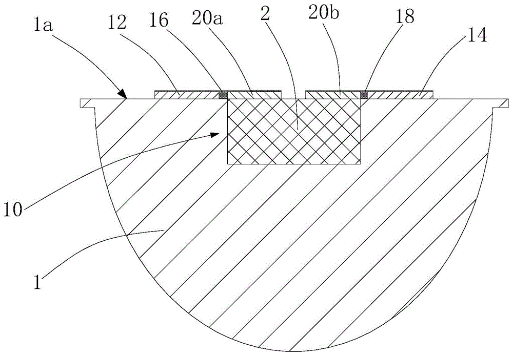
图1示出了实施例1中带透镜式LED封装结构的示意图。FIG. 1 shows a schematic diagram of the encapsulation structure of a lensed LED in
图2示出了实施例2和实施例3中带透镜式LED封装结构的示意图。FIG. 2 shows a schematic diagram of the encapsulation structure of the LED with lens in
图3示出了实施例4中带透镜式LED封装结构的示意图。FIG. 3 shows a schematic diagram of the encapsulation structure of a lensed LED in Embodiment 4. FIG.
图4示出了实施例4中带透镜式LED封装结构的另一示意图。FIG. 4 shows another schematic diagram of the encapsulation structure of the LED with lens in Embodiment 4. FIG.
具体实施方式Detailed ways
为进一步说明各实施例,本发明提供有附图。这些附图为本发明揭露内容的一部分,其主要用以说明实施例,并可配合说明书的相关描述来解释实施例的运作原理。配合参考这些内容,本领域普通技术人员应能理解其他可能的实施方式以及本发明的优点。图中的组件并未按比例绘制,而类似的组件符号通常用来表示类似的组件。To further illustrate the various embodiments, the present invention is provided with accompanying drawings. These drawings are part of the disclosure of the present invention, which are mainly used to illustrate the embodiments, and can be combined with the relevant descriptions in the specification to explain the operating principles of the embodiments. With reference to these contents, those skilled in the art should understand other possible implementations and advantages of the present invention. Components in the figures are not drawn to scale, and similar component symbols are generally used to denote similar components.
现结合附图和具体实施方式对本发明进一步说明。The present invention will be further described in conjunction with the accompanying drawings and specific embodiments.
实施例1Example 1
如图1所示,本发明提供了一种带透镜式LED封装结构,包括透镜1和倒装LED芯片2,所述透镜的入光面1a的中部具有一内凹的腔体10,所述透镜的入光面上还设有位于腔体的周缘并且相互绝缘的第一金属层12和第二金属层14,所述倒装LED芯片2安装在腔体10内,并且该倒装LED芯片2的两个电极20a和20b裸露在腔体外,倒装LED芯片的两个电极(20a、20b)分别与第一金属层12和第二金属层14相电连接。其中腔体10内凹的深度与倒装LED芯片2的厚度相同或者略大于倒装LED芯片2的厚度,因此倒装芯片裸露出的两个电极(20a、20b)和第一金属层12和第二金属层14基本处于同一水平面上,因此两个电极与各自电连接的第一金属层或第二金属层共同成为该封装结构的两个焊盘,增加了焊盘的面积,使得该封装结构能够更简单的直接焊接到基板上。As shown in Figure 1, the present invention provides a lensed LED packaging structure, including a
参考图1,作为该封装结构的一种优选方案,所述带透镜式LED封装结构还具有第三金属层16和第四金属层18,所述第三金属层16覆盖在第一金属层12以及与第一金属层相电连接的电极20a上,所述第四金属层18覆盖在第二金属层14以及与第二金属层相电连接的电极20b上,所述第三金属层16和第四金属层18之间相互绝缘,即第三金属层16和第四金属层18成为该封装结构的两个焊盘。需要明确的是,第三金属层与第一金属层以及和第一金属层相电连接的电极都相电连接,第四金属层与第二金属层以及和第二金属层相电连接的电极都相电连接。Referring to FIG. 1 , as a preferred solution of the packaging structure, the lensed LED packaging structure also has a
作为第三金属层16和第四金属层18的一个优选的方案,所述第三金属层和第四金属层由磁控溅射、电镀或者蒸镀的方式形成。第三金属层和第四金属层的材料为可焊金属,例如铜、银、金、镍或者含有铜、银、金、镍这些金属的合金。As a preferred solution of the
优选第三金属层和第四金属层的厚度为40-100um。Preferably, the thickness of the third metal layer and the fourth metal layer is 40-100um.
实施例2Example 2
本实施例提供的一种带透镜式LED封装结构与实施例1中的带透镜式LED封装结构大致相同,其差异点在于,参考图2,所述腔体10内还具有透光的固晶胶30,所述倒装LED芯片2通过该固晶胶固定到透镜上。在操作时可以先将固定胶30点到透镜的腔体内,然后把倒装LED芯片放置到腔体内,施加压力将倒装芯片和固定胶之间的空气排出,加热将固定胶固化,即可将倒装芯片固定到透镜上。采用透明固晶胶固定倒装LED芯片的方式不仅操作方便,而且可以排出倒装LED芯片与透镜之间的空气,增加其散热效果。The lensed LED package structure provided in this embodiment is roughly the same as the lensed LED package structure in Example 1, the difference is that, referring to FIG. 2 , the
实施例3Example 3
本实施例提供的一种带透镜式LED封装结构与实施例1中的带透镜式LED封装结构大致相同,其差异点在于,参考图2,所述倒装LED芯片2与腔体10的内壁之间的间隙内填充有导热胶40,导热胶40可以排出倒装LED芯片与腔体的内壁之间的空气,增加其散热效果。其中所述导热胶优选由硅胶以及纳米氧化钛和/或纳米氧化铝制成。The lensed LED package structure provided in this embodiment is substantially the same as the lensed LED package structure in Example 1, the difference is that, referring to FIG. 2 , the flip-
实施例4Example 4
本实施例提供的一种带透镜式LED封装结构与实施例1中的带透镜式LED封装结构大致相同,其差异点在于,参考图3,所述透镜的出光面1b上还设有荧光粉层50。其中荧光粉层根据所需的色温以及显色指数来配置,荧光粉层可以采用涂覆或者molding(成型)的方式固定在透镜的出光面上。The LED packaging structure with a lens provided in this embodiment is roughly the same as the LED packaging structure with a lens in
参考图4,作为荧光粉层的另一种实施例,所述透镜的入光面1a和出光面1b之间具有一夹层6,所述夹层6内填充有荧光粉层(图中未示出)。参考图4,在夹层6上设有均与夹层相连通的两个通孔6a和6b,混合有荧光粉的胶体从其中一个通孔6a或者6b中注入到夹层中,使混合有荧光粉的胶体填充满整个夹层,再将胶体加热固化即可实现在夹层6中填充荧光粉层。Referring to Fig. 4, as another embodiment of the phosphor layer, there is an interlayer 6 between the light incident surface 1a and the
上述两个荧光粉层的实现方式都使得荧光粉层与倒装LED芯片隔离,可以减少热量的集中,而位于夹层中的荧光粉层还可以避免在操作中对荧光粉层的损坏。Both of the above two phosphor layer implementation methods isolate the phosphor layer from the flip-chip LED chip, which can reduce heat concentration, and the phosphor layer located in the interlayer can also avoid damage to the phosphor layer during operation.
实施例5Example 5
本发明还提供了一种带透镜式LED封装结构的封装方法,包括以下步骤,The present invention also provides a method for encapsulating a lens-type LED encapsulation structure, comprising the following steps,
S1、提供透镜,所述透镜的入光面的中部具有一内凹的腔体,所述透镜的入光面上还设有位于腔体的周缘并且相互绝缘的第一金属层和第二金属层;S1. Provide a lens, the middle part of the light incident surface of the lens has a concave cavity, and the light incident surface of the lens is also provided with a first metal layer and a second metal layer located on the periphery of the cavity and insulated from each other layer;
S2、将具有凹腔的透镜倒置在平台上,使其凹腔朝上,在凹腔内点透明的固晶胶,以电极朝上的方式将倒装LED芯片放置在凹腔内;S2. Put the lens with concave cavity upside down on the platform so that the concave cavity faces upwards, point transparent crystal-bonding glue in the concave cavity, and place the flip-chip LED chip in the concave cavity with the electrodes facing upwards;
S3、固化固晶胶,使倒装LED芯片固定在凹腔内;S3, solidifying the die-bonding glue, so that the flip-chip LED chip is fixed in the concave cavity;
S4、在倒装LED芯片和凹腔的间隙内填充导热胶;S4, filling the gap between the flip-chip LED chip and the concave cavity with thermal conductive glue;
S5、固化导热胶;S5, curing thermally conductive adhesive;
S6、形成金属层,金属层将倒装LED芯片的两个电极分别与透镜上的两个相互绝缘的金属层电连接起来。S6, forming a metal layer, the metal layer electrically connects the two electrodes of the flip-chip LED chip with the two mutually insulated metal layers on the lens respectively.
优选的,还包括以下步骤,Preferably, the following steps are also included,
S7、在透镜上形成荧光粉层;S7, forming a phosphor layer on the lens;
S8、固化荧光粉层。S8, curing the phosphor layer.
尽管结合优选实施方案具体展示和介绍了本发明,但所属领域的技术人员应该明白,在不脱离所附权利要求书所限定的本发明的精神和范围内,在形式上和细节上可以对本发明做出各种变化,均为本发明的保护范围。Although the present invention has been particularly shown and described in conjunction with preferred embodiments, it will be understood by those skilled in the art that changes in form and details may be made to the present invention without departing from the spirit and scope of the invention as defined by the appended claims. Making various changes is within the protection scope of the present invention.
Claims (10)
Priority Applications (1)
| Application Number | Priority Date | Filing Date | Title |
|---|---|---|---|
| CN201710544822.XA CN107123721B (en) | 2017-07-06 | 2017-07-06 | A kind of encapsulation structure and encapsulation method of LED with lens |
Applications Claiming Priority (1)
| Application Number | Priority Date | Filing Date | Title |
|---|---|---|---|
| CN201710544822.XA CN107123721B (en) | 2017-07-06 | 2017-07-06 | A kind of encapsulation structure and encapsulation method of LED with lens |
Publications (2)
| Publication Number | Publication Date |
|---|---|
| CN107123721A CN107123721A (en) | 2017-09-01 |
| CN107123721B true CN107123721B (en) | 2023-07-07 |
Family
ID=59731111
Family Applications (1)
| Application Number | Title | Priority Date | Filing Date |
|---|---|---|---|
| CN201710544822.XA Active CN107123721B (en) | 2017-07-06 | 2017-07-06 | A kind of encapsulation structure and encapsulation method of LED with lens |
Country Status (1)
| Country | Link |
|---|---|
| CN (1) | CN107123721B (en) |
Families Citing this family (5)
| Publication number | Priority date | Publication date | Assignee | Title |
|---|---|---|---|---|
| CN112133810B (en) * | 2020-10-29 | 2022-06-07 | 深圳市广社照明科技有限公司 | Long-range phosphor powder large-angle scattering patch LED |
| US11929453B2 (en) * | 2021-04-12 | 2024-03-12 | Bolb Inc. | Light-emitting diode package using fluid encapsulate |
| CN113659053B (en) * | 2021-09-07 | 2024-02-27 | 中山市木林森电子有限公司 | A CSP lamp bead packaging structure and its manufacturing process |
| CN115986042A (en) * | 2021-10-15 | 2023-04-18 | 江西晶亮光电科技协同创新有限公司 | A kind of micro-LED packaging structure and packaging method thereof |
| CN117239047B (en) * | 2023-11-14 | 2024-03-12 | 深圳市安卓安科技有限公司 | LED packaging structure, LED module and LCD display applying LED packaging structure |
Citations (5)
| Publication number | Priority date | Publication date | Assignee | Title |
|---|---|---|---|---|
| CN101958389A (en) * | 2010-07-30 | 2011-01-26 | 晶科电子(广州)有限公司 | LED surface mounting structure for silicon substrate integrated with functional circuits and packaging method thereof |
| CN201904369U (en) * | 2010-07-30 | 2011-07-20 | 晶科电子(广州)有限公司 | LED (light emitting diode) surface-mounting package structure based on silicon substrate |
| CN202474017U (en) * | 2011-12-20 | 2012-10-03 | 中山市世耀光电科技有限公司 | Packaging structure of LED light source |
| CN103296174A (en) * | 2013-05-03 | 2013-09-11 | 华中科技大学 | Wafer level packaging structure, method and product for LED flip chip |
| WO2017020681A1 (en) * | 2015-08-03 | 2017-02-09 | 苏文藏 | Led package structure eliminating light spot and improving heat dissipation effect |
Family Cites Families (1)
| Publication number | Priority date | Publication date | Assignee | Title |
|---|---|---|---|---|
| US9966514B2 (en) * | 2015-07-02 | 2018-05-08 | Xiamen Sanan Optoelectronics Technology Co., Ltd. | Light emitting diode package structure and fabrication method |
-
2017
- 2017-07-06 CN CN201710544822.XA patent/CN107123721B/en active Active
Patent Citations (5)
| Publication number | Priority date | Publication date | Assignee | Title |
|---|---|---|---|---|
| CN101958389A (en) * | 2010-07-30 | 2011-01-26 | 晶科电子(广州)有限公司 | LED surface mounting structure for silicon substrate integrated with functional circuits and packaging method thereof |
| CN201904369U (en) * | 2010-07-30 | 2011-07-20 | 晶科电子(广州)有限公司 | LED (light emitting diode) surface-mounting package structure based on silicon substrate |
| CN202474017U (en) * | 2011-12-20 | 2012-10-03 | 中山市世耀光电科技有限公司 | Packaging structure of LED light source |
| CN103296174A (en) * | 2013-05-03 | 2013-09-11 | 华中科技大学 | Wafer level packaging structure, method and product for LED flip chip |
| WO2017020681A1 (en) * | 2015-08-03 | 2017-02-09 | 苏文藏 | Led package structure eliminating light spot and improving heat dissipation effect |
Also Published As
| Publication number | Publication date |
|---|---|
| CN107123721A (en) | 2017-09-01 |
Similar Documents
| Publication | Publication Date | Title |
|---|---|---|
| US10276753B2 (en) | LED flip-chip package substrate and LED package structure | |
| CN107123721B (en) | A kind of encapsulation structure and encapsulation method of LED with lens | |
| CN104851961B (en) | The chip-scale packaging method and structure of luminescent device | |
| TWI528508B (en) | High-power light-emitting diode ceramic package manufacturing method | |
| CN100438111C (en) | Manufacturing method of light-emitting diode packaging structure | |
| CN103855259B (en) | LED encapsulation method | |
| CN106920870B (en) | A high-power ultraviolet LED chip eutectic welding flip-chip structure | |
| CN202067790U (en) | LED encapsulation structure for silicon through hole of wafer-level glass cavity | |
| CN109192722A (en) | A LED flip-chip packaging process | |
| CN105428472A (en) | Manufacturing method for ultraviolet LED device | |
| CN104282831B (en) | A kind of LED encapsulation structure and packaging technology | |
| CN102779815A (en) | Packaging Structure of Light Emitting Diode and Its Manufacturing Method | |
| CN102437267B (en) | Light-emitting chip packaging structure of metal substrate | |
| CN102447044B (en) | Insulating base light-emitting chip packaging structure | |
| CN105023922A (en) | Heat sink structure double-carrier LED drive circuit package and manufacturing method thereof | |
| CN109166949A (en) | A kind of flip LED device and preparation method thereof | |
| CN102297351A (en) | LED (light emitting diode) light source module and manufacturing method thereof | |
| CN103545436A (en) | LED (light emitting diode) packaging structure with sapphire substrate and packaging method for LED packaging structure | |
| CN103855278B (en) | A kind of LED encapsulation structure and luminaire | |
| TWI528596B (en) | Light-emitting diode package structure and manufacturing method thereof | |
| CN204885205U (en) | Flip -chip LED packaging structure | |
| CN103325934A (en) | Light-emitting diode packaging structure and manufacture method thereof | |
| CN202585408U (en) | Structure improvement of multi-layer array type LED light engine | |
| CN218385264U (en) | LED device and LED equipment | |
| TWI597867B (en) | Led flip-chip packaging substrate and led package structure |
Legal Events
| Date | Code | Title | Description |
|---|---|---|---|
| PB01 | Publication | ||
| PB01 | Publication | ||
| SE01 | Entry into force of request for substantive examination | ||
| SE01 | Entry into force of request for substantive examination | ||
| TA01 | Transfer of patent application right |
Effective date of registration: 20230615 Address after: Building A, Building 3, No. 78 Baoshi East Road, Shuitian Community, Shiyan Street, Bao'an District, Shenzhen City, Guangdong Province, 518000 Applicant after: Shenzhen Yongji Photoelectric Technology Co.,Ltd. Address before: No. 8021, Xiang'an West Road, torch high tech Zone (Xiang'an) Industrial Zone, Xiamen, Fujian Province Applicant before: XIAMEN DACOL PHOTOELECTRONICS TECHNOLOGY Co.,Ltd. |
|
| TA01 | Transfer of patent application right | ||
| GR01 | Patent grant | ||
| GR01 | Patent grant |