CN107546112B - SiC ohmic contact structure and manufacturing method thereof - Google Patents
SiC ohmic contact structure and manufacturing method thereof Download PDFInfo
- Publication number
- CN107546112B CN107546112B CN201710583808.0A CN201710583808A CN107546112B CN 107546112 B CN107546112 B CN 107546112B CN 201710583808 A CN201710583808 A CN 201710583808A CN 107546112 B CN107546112 B CN 107546112B
- Authority
- CN
- China
- Prior art keywords
- layer
- magnetron sputtering
- sic
- sputtering process
- tasi
- Prior art date
- Legal status (The legal status is an assumption and is not a legal conclusion. Google has not performed a legal analysis and makes no representation as to the accuracy of the status listed.)
- Active
Links
Images


Landscapes
- Electrodes Of Semiconductors (AREA)
Abstract
本发明涉及一种SiC欧姆接触结构及其制作方法,包括:制作SiC衬底;在所述衬底表面依次淀积第一Ni层、Ti层、第二Ni层、TaSi2层和Pt层;退火处理以完成所述SiC欧姆接触结构的制作。本发明提供的SiC欧姆接触提高了欧姆接触的热稳定性和抗氧化性能。
The invention relates to a SiC ohmic contact structure and a manufacturing method thereof, comprising: manufacturing a SiC substrate; depositing a first Ni layer, a Ti layer, a second Ni layer, a TaSi 2 layer and a Pt layer on the surface of the substrate in sequence; Annealing treatment is performed to complete the fabrication of the SiC ohmic contact structure. The SiC ohmic contact provided by the present invention improves the thermal stability and oxidation resistance of the ohmic contact.
Description
技术领域technical field
本发明属碳化硅器件制造领域,特别涉及一种SiC欧姆接触结构及其制作方法。The invention belongs to the field of silicon carbide device manufacturing, in particular to a SiC ohmic contact structure and a manufacturing method thereof.
背景技术Background technique
相比于传统的锗、硅材料,第三代宽带隙半导体碳化硅的优势主要包括:电场承受能力约为硅材料十倍,禁带宽度约为硅材料的三倍,导热系数约为硅材料三倍等。以上材料特性使得它在极端温度(尤其是高温)与大电压、高频率和高功率以及强辐射等条件下展现了传统的硅基器件无法比拟的优势。Compared with traditional germanium and silicon materials, the advantages of the third-generation wide-bandgap semiconductor silicon carbide mainly include: the electric field withstand capability is about ten times that of silicon materials, the band gap is about three times that of silicon materials, and the thermal conductivity is about silicon materials. triple etc. The above material characteristics make it show the incomparable advantages of traditional silicon-based devices under the conditions of extreme temperature (especially high temperature) and large voltage, high frequency and high power, and strong radiation.
欧姆接触是碳化硅器件应用于高温、易氧化等极端环境中的关键影响因素之一,它的目的在于实现当电极处在施加正向电压时能承载尽可能小的压降,以此,来保证器件的性能。假设欧姆接触退化或者失效,势必影响器件的开启电阻,严重时会影响器件性能,乃至令器件失效。所以设计热稳定性良好,抗氧化的欧姆接触电极显得尤为必要。Ohmic contact is one of the key factors for silicon carbide devices to be used in extreme environments such as high temperature and easy oxidation. Its purpose is to achieve the smallest possible voltage drop when the electrode is in a forward voltage. Guaranteed device performance. Assuming that the ohmic contact degrades or fails, it will inevitably affect the turn-on resistance of the device, and in severe cases, it will affect the performance of the device, and even cause the device to fail. Therefore, it is particularly necessary to design an ohmic contact electrode with good thermal stability and anti-oxidation.
目前,碳化硅欧姆接触金属或者合金层面临问题包括抗氧化能力弱,在空气中即被氧化;热稳定性差,高温下出现退化或者失效;硬度低,容易被机械损伤等缺点,这些缺点会使得欧姆接触电极可靠性降低,严重限制其应用环境与范围,进而令碳化硅器件的应用范围与可靠性受到诸多影响与限制。At present, the problems of silicon carbide ohmic contact metal or alloy layer include weak oxidation resistance, which is oxidized in the air; poor thermal stability, degradation or failure at high temperature; low hardness, easy to be mechanically damaged and other shortcomings, these shortcomings will make The reliability of the ohmic contact electrode is reduced, which severely limits its application environment and scope, and further affects and limits the application scope and reliability of silicon carbide devices.
发明内容SUMMARY OF THE INVENTION
鉴于以上背景,本发明旨在实现一种耐高温、抗氧化的欧姆接触结构及其制作方法。In view of the above background, the present invention aims to realize an ohmic contact structure with high temperature resistance and oxidation resistance and a manufacturing method thereof.
一方面,本发明提供了一种SiC欧姆接触结构的制作方法,包括:In one aspect, the present invention provides a method for fabricating a SiC ohmic contact structure, comprising:
(a)制作SiC衬底;(a) making SiC substrate;
(b)在所述衬底表面依次淀积第一Ni层、Ti层、第二Ni层、TaSi2层和Pt层;(b) sequentially depositing a first Ni layer, a Ti layer, a second Ni layer, a TaSi 2 layer and a Pt layer on the surface of the substrate;
(c)进行第一退火处理以完成所述SiC欧姆接触结构的制作。(c) performing a first annealing treatment to complete the fabrication of the SiC ohmic contact structure.
在本发明的一个实施例中,步骤(a)可以包括:In one embodiment of the present invention, step (a) may include:
(a1)选取4H-SiC衬底并对所述4H-SiC衬底进行标准RCA清洗;(a1) selecting a 4H-SiC substrate and performing standard RCA cleaning on the 4H-SiC substrate;
(a2)利用等离子体增强化学的气相沉积法(Plasma Enhanced Chemical VaporDeposition,PECVD)工艺,在所述4H-SiC衬底表面淀积厚度为100nm的氧化层;(a2) using a plasma enhanced chemical vapor deposition (Plasma Enhanced Chemical VaporDeposition, PECVD) process to deposit an oxide layer with a thickness of 100 nm on the surface of the 4H-SiC substrate;
(a3)刻蚀所述氧化层形成离子注入窗口,利用离子注入工艺,对所述4H-SiC衬底表面进行N+、P+离子注入形成N型掺杂区和P型掺杂区;(a3) etching the oxide layer to form an ion implantation window, and using an ion implantation process to perform N + and P + ion implantation on the surface of the 4H-SiC substrate to form an N-type doped region and a P-type doped region;
(a4)刻蚀掉剩余的氧化层,并进行第二退火处理。(a4) The remaining oxide layer is etched away, and a second annealing treatment is performed.
在本发明的一个实施例中,步骤(a3)中所述N型掺杂区的掺杂源为Al,掺杂浓度为1.0×1020cm-3;所述P型掺杂区的掺杂源为N,掺杂浓度为3.0×1020cm-3。In an embodiment of the present invention, in step (a3), the doping source of the N-type doping region is Al, and the doping concentration is 1.0×10 20 cm −3 ; the doping of the P-type doping region is Al. The source was N, and the doping concentration was 3.0×10 20 cm −3 .
在本发明的一个实施例中,步骤(a4)中所述第二退火处理的温度为1700℃,退火时间为30min。In an embodiment of the present invention, the temperature of the second annealing treatment in step (a4) is 1700° C., and the annealing time is 30 minutes.
在本发明的一个实施例中,步骤(b)可以包括:In one embodiment of the present invention, step (b) may include:
(b1)利用直流磁控溅射工艺,在所述衬底表面淀积所述第一Ni层;所述直流磁控溅射工艺的淀积功率为100W、淀积速率为9.8nm/min;(b1) using a DC magnetron sputtering process to deposit the first Ni layer on the surface of the substrate; the deposition power of the DC magnetron sputtering process is 100W and the deposition rate is 9.8nm/min;
(b2)利用直流磁控溅射工艺,在所述第一Ni层表面淀积所述Ti层;所述直流磁控溅射工艺的淀积功率为100W、淀积速率为2.9nm/min;(b2) using a DC magnetron sputtering process to deposit the Ti layer on the surface of the first Ni layer; the deposition power of the DC magnetron sputtering process is 100W and the deposition rate is 2.9nm/min;
(b3)利用直流磁控溅射工艺,在所述Ti层表面淀积所述第二Ni层;所述直流磁控溅射工艺的淀积功率为100W、淀积速率为9.8nm/min;(b3) using a DC magnetron sputtering process to deposit the second Ni layer on the surface of the Ti layer; the deposition power of the DC magnetron sputtering process is 100W and the deposition rate is 9.8nm/min;
(b4)利用射频磁控溅射工艺,在所述第二Ni层表面淀积所述TaSi2层;所述射频磁控溅射工艺的淀积功率为60W、淀积速率为2.9nm/min;(b4) using a radio frequency magnetron sputtering process to deposit the TaSi 2 layer on the surface of the second Ni layer; the deposition power of the radio frequency magnetron sputtering process is 60W and the deposition rate is 2.9nm/min ;
(b5)利用直流磁控溅射工艺,在所述TaSi2层表面淀积所述Pt层;所述直流磁控溅射工艺的淀积功率为100W、淀积速率为2.9nm/min。(b5) Using a DC magnetron sputtering process to deposit the Pt layer on the surface of the TaSi 2 layer; the deposition power of the DC magnetron sputtering process is 100W and the deposition rate is 2.9nm/min.
在本发明的一个实施例中,淀积时的磁控溅射腔的腔内真空度≤5e-6mTorr。In an embodiment of the present invention, the vacuum degree in the magnetron sputtering chamber during deposition is ≤5e -6 mTorr.
在本发明的一个实施例中,所述第一Ni层厚度为30nm、所述Ti层厚度为100nm、所述第二Ni层厚度为30nm、所述TaSi2层厚度为300nm以及所述Pt层厚度为200nm。In one embodiment of the present invention, the thickness of the first Ni layer is 30 nm, the thickness of the Ti layer is 100 nm, the thickness of the second Ni layer is 30 nm, the thickness of the TaSi 2 layer is 300 nm, and the thickness of the Pt layer is 30 nm. The thickness is 200nm.
在本发明的一个实施例中,步骤(c)中第一退火工艺中的退火温度为975℃,退火时间为2min。In an embodiment of the present invention, the annealing temperature in the first annealing process in step (c) is 975° C., and the annealing time is 2 min.
再一方面,本发明提供了一种SiC欧姆接触结构,包括:SiC衬底,以及依次设置于所述SiC衬底上的第一Ni层、Ti层、第二Ni层、TaSi2层和Pt层。In yet another aspect, the present invention provides a SiC ohmic contact structure, comprising: a SiC substrate, and a first Ni layer, a Ti layer, a second Ni layer, a TaSi 2 layer and a Pt layer that are sequentially arranged on the SiC substrate Floor.
与现有技术相比,本发明提供了一种利用Pt/TaSi2/Ni/Ti/Ni/SiC结构制作欧姆接触的方法,该结构提高了欧姆接触的热稳定性和抗氧化性能;不仅在空气中,500℃条件下展现了良好的I-V特性,而且在经过300h的500℃的老化测试之后没有出现退化。Compared with the prior art, the present invention provides a method for making an ohmic contact by using a Pt/TaSi 2 /Ni/Ti/Ni/SiC structure, which improves the thermal stability and oxidation resistance of the ohmic contact; In air, it exhibits good IV characteristics at 500 °C, and no degradation occurs after 300 h of aging at 500 °C.
附图说明Description of drawings
为了更清楚地说明本发明实施例的技术方案,下面将对实施例描述中所需要使用的附图作简单地介绍,显而易见地,下面描述中的附图仅仅是本发明的一些实施例,对于本领域普通技术人员来讲,在不付出创造性劳动的前提下,还可以根据这些附图获得其他的附图。In order to illustrate the technical solutions of the embodiments of the present invention more clearly, the following briefly introduces the accompanying drawings used in the description of the embodiments. Obviously, the drawings in the following description are only some embodiments of the present invention. For those of ordinary skill in the art, other drawings can also be obtained from these drawings without any creative effort.
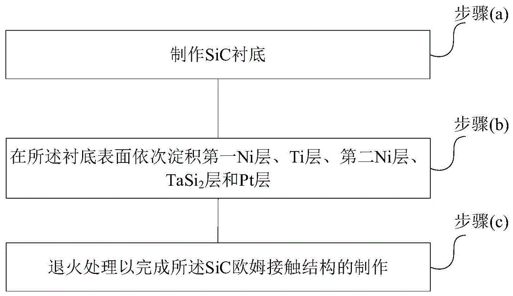
图1为本发明实施例提供的一种SiC欧姆接触工艺流程图;1 is a process flow diagram of a SiC ohmic contact provided by an embodiment of the present invention;
图2为本发明实施例提供的一种Pt/Ti/SiC结构退火前后的XRD元素图;Fig. 2 is the XRD element diagram of a kind of Pt/Ti/SiC structure before and after annealing provided by the embodiment of the present invention;
图3为本发明实施例提供的一种退火之后器件表面的扫描电子显微镜图像;3 is a scanning electron microscope image of a device surface after annealing provided by an embodiment of the present invention;
图4为本发明实施例提供的一种Pt/TaSi2/Ni/Ti/Ni/SiC结构退火前后的XRD元素图;4 is an XRD elemental diagram of a Pt/TaSi 2 /Ni/Ti/Ni/SiC structure before and after annealing provided by an embodiment of the present invention;
图5为本发明实施例提供的一种Pt/TaSi2/Ni/Ti/Ni/SiC、Ti/Pt结构N、P型欧姆接触975℃退火之后的I-V曲线图;5 is an IV curve diagram of a Pt/TaSi 2 /Ni/Ti/Ni/SiC, Ti/Pt structure N, P-type ohmic contact provided by an embodiment of the present invention after annealing at 975°C;
图6为本发明实施例提供的一种Pt/TaSi2/Ni/Ti/Ni/SiC、Ti/Pt结构N、P型欧姆接触特征导通电阻随老化时间的变化曲线图;Fig. 6 is a kind of Pt/TaSi 2 /Ni/Ti/Ni/SiC, Ti/Pt structure N, P-type ohmic contact characteristic on-resistance variation curve diagram with aging time provided by the embodiment of the present invention;
图7为本发明实施例提供的一种CTLM结构版图;FIG. 7 is a layout of a CTLM structure provided by an embodiment of the present invention;
图8为本发明实施例提供的一种剥离之后金属结构显微镜图片;以及FIG. 8 is a microscope picture of a metal structure after peeling provided by an embodiment of the present invention; and
图9为本发明实施例提供的一种SiC欧姆接触结构剖面图。FIG. 9 is a cross-sectional view of a SiC ohmic contact structure according to an embodiment of the present invention.
具体实施方式Detailed ways
下面将结合本发明实施例中的附图,对本发明实施例中的技术方案进行清楚、完整地描述,显然,所描述的实施例仅仅是本发明一部分实施例,而不是全部的实施例。基于本发明中的实施例,本领域普通技术人员在没有作出创造性劳动前提下所获得的所有其他实施例,都属于本发明保护的范围。The technical solutions in the embodiments of the present invention will be clearly and completely described below with reference to the accompanying drawings in the embodiments of the present invention. Obviously, the described embodiments are only a part of the embodiments of the present invention, but not all of the embodiments. Based on the embodiments of the present invention, all other embodiments obtained by those of ordinary skill in the art without creative efforts shall fall within the protection scope of the present invention.
实施例一Example 1
请参见图1,图1为本发明实施例提供的一种SiC欧姆接触工艺流程图,包括:Please refer to FIG. 1. FIG. 1 is a process flow diagram of a SiC ohmic contact provided by an embodiment of the present invention, including:
(a)制作SiC衬底;(a) making SiC substrate;
(b)在所述衬底表面依次淀积第一Ni层、Ti层、第二Ni层、TaSi2层和Pt层;(b) sequentially depositing a first Ni layer, a Ti layer, a second Ni layer, a TaSi 2 layer and a Pt layer on the surface of the substrate;
(c)进行第一退火处理以完成所述SiC欧姆接触结构的制作。(c) performing a first annealing treatment to complete the fabrication of the SiC ohmic contact structure.
优选地,步骤(a)可以包括:Preferably, step (a) may comprise:
(a1)选取4H-SiC衬底并对所述4H-SiC衬底进行标准RCA清洗;(a1) selecting a 4H-SiC substrate and performing standard RCA cleaning on the 4H-SiC substrate;
(a2)利用PECVD工艺,在所述4H-SiC衬底表面淀积厚度为100nm的氧化层;(a2) Utilize PECVD process to deposit an oxide layer with a thickness of 100 nm on the surface of the 4H-SiC substrate;
(a3)刻蚀所述氧化层形成离子注入窗口,利用离子注入工艺,对所述4H-SiC衬底表面进行N+、P+离子注入形成N型掺杂区和P型掺杂区;(a3) etching the oxide layer to form an ion implantation window, and using an ion implantation process to perform N + and P + ion implantation on the surface of the 4H-SiC substrate to form an N-type doped region and a P-type doped region;
(a4)刻蚀掉剩余的氧化层,并进行第二退火处理。(a4) The remaining oxide layer is etched away, and a second annealing treatment is performed.
其中,步骤(a3)中所述N型掺杂区的掺杂源为Al,掺杂浓度为1.0×1020cm-3;所述P型掺杂区的掺杂源为N,掺杂浓度为3.0×1020cm-3。Wherein, in step (a3), the doping source of the N-type doping region is Al, and the doping concentration is 1.0×10 20 cm −3 ; the doping source of the P-type doping region is N, and the doping concentration is N is 3.0×10 20 cm -3 .
进一步地,步骤(a4)中所述第二退火处理的温度为1700℃,退火时间为30min。Further, the temperature of the second annealing treatment in step (a4) is 1700° C., and the annealing time is 30 min.
优选地,步骤(b)可以包括:Preferably, step (b) may comprise:
(b1)利用直流磁控溅射工艺,在所述衬底表面淀积所述第一Ni层;所述直流磁控溅射工艺的淀积功率为100W、淀积速率为9.8nm/min;(b1) using a DC magnetron sputtering process to deposit the first Ni layer on the surface of the substrate; the deposition power of the DC magnetron sputtering process is 100W and the deposition rate is 9.8nm/min;
(b2)利用直流磁控溅射工艺,在所述第一Ni层表面淀积所述Ti层;所述直流磁控溅射工艺的淀积功率为100W、淀积速率为2.9nm/min;(b2) using a DC magnetron sputtering process to deposit the Ti layer on the surface of the first Ni layer; the deposition power of the DC magnetron sputtering process is 100W and the deposition rate is 2.9nm/min;
(b3)利用直流磁控溅射工艺,在所述Ti层表面淀积所述第二Ni层;所述直流磁控溅射工艺的淀积功率为100W、淀积速率为9.8nm/min;(b3) using a DC magnetron sputtering process to deposit the second Ni layer on the surface of the Ti layer; the deposition power of the DC magnetron sputtering process is 100W and the deposition rate is 9.8nm/min;
(b4)利用射频磁控溅射工艺,在所述第二Ni层表面淀积所述TaSi2层;所述射频磁控溅射工艺的淀积功率为60W、淀积速率为2.9nm/min;(b4) using a radio frequency magnetron sputtering process to deposit the TaSi 2 layer on the surface of the second Ni layer; the deposition power of the radio frequency magnetron sputtering process is 60W and the deposition rate is 2.9nm/min ;
(b5)利用直流磁控溅射工艺,在所述TaSi2层表面淀积所述Pt层;所述直流磁控溅射工艺的淀积功率为100W、淀积速率为2.9nm/min。(b5) Using a DC magnetron sputtering process to deposit the Pt layer on the surface of the TaSi 2 layer; the deposition power of the DC magnetron sputtering process is 100W and the deposition rate is 2.9nm/min.
其中,步骤(b)中淀积时的磁控溅射腔的腔内真空度≤5e-6mTorr。Wherein, the vacuum degree in the magnetron sputtering chamber during deposition in step (b) is ≤5e -6 mTorr.
优选地,所述第一Ni层厚度为30nm、所述Ti层厚度为100nm、所述第二Ni层厚度为30nm、所述TaSi2层厚度为300nm以及所述Pt层厚度为200nm。Preferably, the thickness of the first Ni layer is 30 nm, the thickness of the Ti layer is 100 nm, the thickness of the second Ni layer is 30 nm, the thickness of the TaSi 2 layer is 300 nm and the thickness of the Pt layer is 200 nm.
优选地,步骤(c)中第一退火工艺中的退火温度为975℃,退火时间为2min。Preferably, the annealing temperature in the first annealing process in step (c) is 975° C., and the annealing time is 2 min.
其中,第一Ni层与SiC产生反应,Ti层可以结合由于Ni与SiC反应产生的C,以免游离态的C原子在表面集聚,而使表面粗糙或者失效。如图2所示,图2为本发明实施例提供的一种Pt/Ti/SiC结构退火前后的XRD元素图,退火后Ti的比例明显减少,而TiC合金比例明显上升。Among them, the first Ni layer reacts with SiC, and the Ti layer can combine the C generated by the reaction between Ni and SiC, so as to prevent free C atoms from agglomerating on the surface, causing the surface to be rough or ineffective. As shown in FIG. 2 , FIG. 2 is an XRD element diagram of a Pt/Ti/SiC structure before and after annealing provided by an embodiment of the present invention. After annealing, the proportion of Ti is significantly reduced, while the proportion of TiC alloy is significantly increased.
第二Ni层作为Ti层与TaSi2层之间的粘附层,能有效降低退火温度,以便同时进行N/P型的退火,同时它能改进接触表面样貌;如图3所示,图3为本发明实施例提供的一种退火之后器件表面的扫描电子显微镜图像,可以看出Ni层还对Ti的向上扩散起到了阻挡作用。The second Ni layer acts as the adhesion layer between the Ti layer and the TaSi 2 layer, which can effectively reduce the annealing temperature so that the N/P type annealing can be performed at the same time, and at the same time, it can improve the contact surface appearance; as shown in Fig. 3, Fig. 3 is a scanning electron microscope image of the device surface after annealing provided in the embodiment of the present invention. It can be seen that the Ni layer also blocks the upward diffusion of Ti.
进一步地,TaSi2层是防止欧姆接触电极氧化的关键,它能有效阻挡O向下扩散,在500℃下,空气中进行300h退火条件后,TaSi2层以下O的比例并没有增大,表明TaSi2层对O的阻挡作用显著。除此之外,TaSi2的分解符合指数形式使得此结构能够长时间有效,因此,令此结构能够暴露在空气中进行老化测试。如图4所示,图4为本发明实施例提供的一种Pt/TaSi2/Ni/Ti/Ni/SiC结构退火前后的XRD元素图,各元素基本保持原来的合金结构,即TaSi2的缓慢分解使得各金属层结构基本维持不变。Further, the TaSi 2 layer is the key to prevent the oxidation of the ohmic contact electrode, which can effectively block the downward diffusion of O. After annealing at 500 °C for 300 h in air, the proportion of O below the TaSi 2 layer did not increase, indicating that The blocking effect of TaSi 2 layer on O is remarkable. In addition, the decomposition of TaSi 2 conforms to the exponential form, which makes the structure effective for a long time, and therefore, allows the structure to be exposed to air for aging tests. As shown in FIG. 4 , FIG. 4 is the XRD element diagram of a Pt/TaSi 2 /Ni/Ti/Ni/SiC structure before and after annealing provided by the embodiment of the present invention, and each element basically maintains the original alloy structure, that is, the TaSi 2 The slow decomposition keeps the structure of each metal layer basically unchanged.
本发明中单纯的Ni/Pt、Ti/Pt结构在高温空气环境下,短时间内即失效。Ni/TaSi2/Pt、Ti/TaSi2/Pt结构难以形成良好的P型欧姆接触电极。Pt/TaSi2/Ni/Ti/Ni/SiC结构同时实现了N、P衬底上的欧姆接触特性,相比于真空或惰性范围内性能较优异的Ti/Pt结构,其特性如图5所示,图5为本发明实施例提供的一种Pt/TaSi2/Ni/Ti/Ni/SiC、Ti/Pt结构N、P型欧姆接触975℃退火之后的I-V曲线图;欧姆接触特性良好。对此结构在空气中进行高温、老化测试,300小时时并未出现严重退化。同时,如图6所示,图6为本发明实施例提供的一种Pt/TaSi2/Ni/Ti/Ni/SiC、Ti/Pt结构N、P型欧姆接触特征导通电阻随老化时间的变化曲线图;在室温与500℃高温条件下,测量其特征导通电阻与Ti/Pt结构作对比。即Pt/TaSi2/Ni/Ti/Ni/SiC在高温、老化条件下有着良好性能,对比于以上其余结构有着很大优势。The pure Ni/Pt and Ti/Pt structures in the present invention will fail in a short period of time in a high-temperature air environment. Ni/TaSi 2 /Pt and Ti/TaSi 2 /Pt structures are difficult to form a good P-type ohmic contact electrode. The Pt/TaSi 2 /Ni/Ti/Ni/SiC structure achieves ohmic contact properties on both N and P substrates. Compared with the Ti/Pt structure with better performance in the vacuum or inert range, its properties are shown in Figure 5. 5 is an IV curve diagram of a Pt/TaSi 2 /Ni/Ti/Ni/SiC, Ti/Pt structure N, P-type ohmic contact after annealing at 975°C provided by an embodiment of the present invention; the ohmic contact characteristics are good. The structure was subjected to high temperature and aging tests in the air, and no serious degradation occurred after 300 hours. At the same time, as shown in FIG. 6 , FIG. 6 is the characteristic on-resistance of a Pt/TaSi 2 /Ni/Ti/Ni/SiC, Ti/Pt structure N, P-type ohmic contact provided by an embodiment of the present invention with aging time Change curve diagram; at room temperature and 500 ℃ high temperature conditions, measure its characteristic on-resistance and compare with Ti/Pt structure. That is, Pt/TaSi 2 /Ni/Ti/Ni/SiC has good performance under high temperature and aging conditions, and has great advantages compared with the other structures above.
实施例二
本发明提出一种利用Pt/TaSi2/Ni/Ti/Ni/SiC结构制作SiC欧姆接触的方法,包括:The present invention proposes a method for making SiC ohmic contact by utilizing a Pt/TaSi 2 /Ni/Ti/Ni/SiC structure, including:
S201,选取4H-SiC衬底,对4H-SiC衬底进行标准RCA清洗;S201, selecting a 4H-SiC substrate, and performing standard RCA cleaning on the 4H-SiC substrate;
S202,利用PECVD工艺,在4H-SiC衬底淀积厚度为100nmSiO2氧化层;S202, using a PECVD process to deposit an SiO2 oxide layer with a thickness of 100 nm on the 4H-SiC substrate;
S203,刻蚀氧化层形成离子注入窗口,对4H-SiC衬底N+或者P+离子注入,形成高掺杂的N区或者P区并进行高温退火;S203, etching the oxide layer to form an ion implantation window, and implanting N + or P + ions into the 4H-SiC substrate to form a highly doped N region or P region and perform high temperature annealing;
S204,刻蚀剩余的氧化层;S204, etching the remaining oxide layer;
S205,在4H-SiC衬底上淀积金属层,金属层由下往上依次包括第一Ni层、Ti层、第二Ni层、TaSi2层和Pt层;S205, depositing a metal layer on the 4H-SiC substrate, the metal layer sequentially includes a first Ni layer, a Ti layer, a second Ni layer, a TaSi 2 layer and a Pt layer from bottom to top;
S206,快速退火以形成欧姆接触。S206, rapid annealing to form an ohmic contact.
优选地,步骤S203中所述N型掺杂区的掺杂源为Al,掺杂浓度为1.0×1020cm-3;所述P型掺杂区的掺杂源为N,掺杂浓度为3.0×1020cm-3。进行高温退火的温度为1700℃,时间为30min。Preferably, in step S203, the doping source of the N-type doping region is Al, and the doping concentration is 1.0×10 20 cm −3 ; the doping source of the P-type doping region is N, and the doping concentration is 3.0×10 20 cm -3 . The high temperature annealing temperature was 1700° C. and the time was 30 min.
优选地,步骤S205中,所使用的淀积方法中,第一Ni层、Ti层、第二Ni层和Pt层采用直流磁控溅射淀积;TaSi2层采用射频磁控溅射淀积;Preferably, in step S205, in the deposition method used, the first Ni layer, the Ti layer, the second Ni layer and the Pt layer are deposited by DC magnetron sputtering; the TaSi 2 layer is deposited by radio frequency magnetron sputtering ;
第一Ni层、Ti层、第二Ni层和Pt层的淀积功率为100W;TaSi2层的淀积功率为60W;The deposition power of the first Ni layer, the Ti layer, the second Ni layer and the Pt layer is 100W; the deposition power of the TaSi 2 layer is 60W;
Ti层、TaSi2层和Pt层的淀积速率为2.9nm/min,第一Ni层和第二Ni层的淀积速率为9.8nm/min;淀积时候的腔内真空度≤5e-6mTorr;The deposition rate of Ti layer, TaSi 2 layer and Pt layer is 2.9nm/min, and the deposition rate of the first Ni layer and the second Ni layer is 9.8nm/min; the vacuum degree of the chamber during deposition is ≤5e -6 mTorr;
第一Ni层和第二Ni层的淀积气流量为24Ar/sccm,Ti层和Pt层的淀积气流量为16Ar/sccm,TaSi2层的淀积气流量为20Ar/sccm。The deposition gas flow rate of the first Ni layer and the second Ni layer is 24Ar/sccm, the deposition gas flow rate of the Ti layer and the Pt layer is 16Ar/sccm, and the deposition gas flow rate of the TaSi 2 layer is 20Ar/sccm.
进一步地,第一Ni层厚度为30nm、Ti层厚度为100nm、第二Ni层厚度为30nm、TaSi2层厚度为300nm以及Pt层厚度为200nm。Further, the thickness of the first Ni layer is 30 nm, the thickness of the Ti layer is 100 nm, the thickness of the second Ni layer is 30 nm, the thickness of the TaSi 2 layer is 300 nm, and the thickness of the Pt layer is 200 nm.
其中,对本实施例中的欧姆接触结构进行性能测试的方法如下:Wherein, the method for performing performance test on the ohmic contact structure in this embodiment is as follows:
步骤一:选取4H-SiC衬底,对4H-SiC衬底进行标准RCA清洗;Step 1: Select a 4H-SiC substrate, and perform standard RCA cleaning on the 4H-SiC substrate;
步骤二:利用PECVD工艺,在4H-SiC衬底淀积厚度为100nmSiO2氧化层;Step 2: deposit an oxide layer of SiO 2 with a thickness of 100 nm on the 4H-SiC substrate by using the PECVD process;
步骤三:刻蚀氧化层形成离子注入窗口,对4H-SiC衬底N+或者P+离子注入,形成高掺杂的N区或者P区并进行高温退火;Step 3: etching the oxide layer to form an ion implantation window, implanting N + or P + ions into the 4H-SiC substrate, forming a highly doped N region or P region and performing high temperature annealing;
步骤四:利用掩膜版进行光刻,形成CTLM图形,去除底胶,利用HF去除自然氧化层以及其他杂质。Step 4: Use the mask to perform photolithography, form CTLM patterns, remove the primer, and use HF to remove the natural oxide layer and other impurities.
进一步地,步骤四中形成CTLM图形如图7所示,图7为本发明实施例提供的一种CTLM结构版图;Further, the CTLM graph formed in step 4 is shown in FIG. 7 , and FIG. 7 is a layout of a CTLM structure provided by an embodiment of the present invention;
优选地,步骤四中HF配比为HF:H2O=1:20。在HF中浸洗2min,之后用清水冲洗去除HF溶液,N2吹干。Preferably, in step 4, the HF ratio is HF:H 2 O=1:20. Immerse in HF for 2 min, then rinse with water to remove the HF solution, and dry with N 2 .
步骤五:在SiC材料上依次淀积第一Ni层、Ti层、第二Ni层、TaSi2层和Pt层;Step 5: sequentially depositing the first Ni layer, the Ti layer, the second Ni layer, the TaSi 2 layer and the Pt layer on the SiC material;
步骤六:金属剥离与快速退火形成欧姆接触结构并对所述欧姆接触结构进行性能测试。Step 6: metal stripping and rapid annealing to form an ohmic contact structure and perform a performance test on the ohmic contact structure.
进一步地,步骤六中金属剥离具体步骤为:将包括4H-SiC衬底和金属层的整个衬底材料置于丙酮中浸泡约10h至光刻胶层上金属层翘起,之后进行超声约3min至翘起金属完全脱落。如图8所示,图8为本发明实施例提供的一种剥离之后金属结构显微镜图片;在显微镜下观察金属环没有粘连。退火的条件为温度975℃,惰性气体的保护氛围中,退火时间2min。Further, the specific steps of metal stripping in
本发明利用Pt/TaSi2/Ni/Ti/Ni/SiC结构制作SiC欧姆接触。首先,Ni与SiC反应。Ti层可以结合由于Ni与SiC反应产生的C,以免游离态的C原子在表面集聚,而使表面粗糙或者失效。退火后Ti的比例明显减少,而TiC合金比例明显上升。第二Ni层作为Ti金属层与TaSi2金属层之间的粘附层,能有效降低退火温度,以便同时进行N/P型的退火,同时它能改进接触表面样貌,而且此镍层还对Ti的向上扩散起到了阻挡作用。TaSi2层是防止欧姆接触电极氧化的关键,它能有效阻挡O向下扩散,通过300h老化测试后,TaSi2层以下O的比例并没有增大,表明TaSi2层对O的阻挡作用显著。The present invention utilizes Pt/TaSi 2 /Ni/Ti/Ni/SiC structure to make SiC ohmic contact. First, Ni reacts with SiC. The Ti layer can combine the C generated by the reaction between Ni and SiC, so as to avoid the accumulation of free C atoms on the surface, which may cause the surface to be rough or fail. After annealing, the proportion of Ti decreased significantly, while the proportion of TiC alloy increased significantly. The second Ni layer acts as the adhesion layer between the Ti metal layer and the TaSi 2 metal layer, which can effectively reduce the annealing temperature so that N/P type annealing can be performed at the same time, and at the same time, it can improve the contact surface appearance, and the nickel layer also It has a blocking effect on the upward diffusion of Ti. The TaSi 2 layer is the key to preventing the oxidation of the ohmic contact electrode. It can effectively block the downward diffusion of O. After 300h aging test, the proportion of O below the TaSi 2 layer does not increase, indicating that the TaSi 2 layer has a significant blocking effect on O.
实施例三Embodiment 3
请参照图9,图9为本发明实施例提供的一种SiC欧姆接触结构剖面图;SiC欧姆接触结构包括:SiC衬底1,以及依次设置于所述SiC衬底上的第一Ni层2、Ti层3、第二Ni层4、TaSi2层5和Pt层6。Please refer to FIG. 9, which is a cross-sectional view of a SiC ohmic contact structure provided by an embodiment of the present invention; the SiC ohmic contact structure includes: a
综上,本文中应用了具体个例对本发明的原理及实施方式进行了阐述,以上实施例的说明只是用于帮助理解本发明的方法及其核心思想;同时,对于本领域的一般技术人员,依据本发明的思想,在具体实施方式及应用范围上均会有改变之处,综上,本说明书内容不应理解为对本发明的限制,本发明的保护范围应以所附的权利要求为准。To sum up, the principles and implementations of the present invention are described with specific examples in this paper, and the descriptions of the above embodiments are only used to help understand the method and the core idea of the present invention; meanwhile, for those of ordinary skill in the art, According to the idea of the present invention, there will be changes in the specific embodiments and application scope. In summary, the contents of this specification should not be construed as limitations to the present invention, and the protection scope of the present invention should be based on the appended claims. .
Claims (8)
Priority Applications (1)
| Application Number | Priority Date | Filing Date | Title |
|---|---|---|---|
| CN201710583808.0A CN107546112B (en) | 2017-07-18 | 2017-07-18 | SiC ohmic contact structure and manufacturing method thereof |
Applications Claiming Priority (1)
| Application Number | Priority Date | Filing Date | Title |
|---|---|---|---|
| CN201710583808.0A CN107546112B (en) | 2017-07-18 | 2017-07-18 | SiC ohmic contact structure and manufacturing method thereof |
Publications (2)
| Publication Number | Publication Date |
|---|---|
| CN107546112A CN107546112A (en) | 2018-01-05 |
| CN107546112B true CN107546112B (en) | 2020-02-07 |
Family
ID=60971130
Family Applications (1)
| Application Number | Title | Priority Date | Filing Date |
|---|---|---|---|
| CN201710583808.0A Active CN107546112B (en) | 2017-07-18 | 2017-07-18 | SiC ohmic contact structure and manufacturing method thereof |
Country Status (1)
| Country | Link |
|---|---|
| CN (1) | CN107546112B (en) |
Families Citing this family (1)
| Publication number | Priority date | Publication date | Assignee | Title |
|---|---|---|---|---|
| CN110349839B (en) * | 2019-06-21 | 2021-03-12 | 全球能源互联网研究院有限公司 | Preparation method of p/n type silicon carbide ohmic contact |
Citations (3)
| Publication number | Priority date | Publication date | Assignee | Title |
|---|---|---|---|---|
| CN103578960A (en) * | 2013-11-20 | 2014-02-12 | 中国科学院微电子研究所 | A method for preparing ohmic contact on the back of SiC substrate |
| US9013002B1 (en) * | 2011-12-02 | 2015-04-21 | The United States Of America As Represented By The Administrator Of National Aeronautics And Space Administration | Iridium interfacial stack (IRIS) |
| CN106683994A (en) * | 2017-01-11 | 2017-05-17 | 电子科技大学 | Manufacturing method of P-type silicon carbide ohmic contact |
-
2017
- 2017-07-18 CN CN201710583808.0A patent/CN107546112B/en active Active
Patent Citations (3)
| Publication number | Priority date | Publication date | Assignee | Title |
|---|---|---|---|---|
| US9013002B1 (en) * | 2011-12-02 | 2015-04-21 | The United States Of America As Represented By The Administrator Of National Aeronautics And Space Administration | Iridium interfacial stack (IRIS) |
| CN103578960A (en) * | 2013-11-20 | 2014-02-12 | 中国科学院微电子研究所 | A method for preparing ohmic contact on the back of SiC substrate |
| CN106683994A (en) * | 2017-01-11 | 2017-05-17 | 电子科技大学 | Manufacturing method of P-type silicon carbide ohmic contact |
Non-Patent Citations (3)
| Title |
|---|
| 《Reliability assessment of Ti/TaSi2/Pt ohmic contacts on SiC after 1000h at 600℃》;Robert S.Okojie;《Journal of Applied Physics》;20020515;第91卷;全文 * |
| Improved Thermal Stability Observed in Ni-Based Ohmic Contacts to n-Type SiC for High-Temperature Applications;ARIEL VIRSHUP等;《Journal of Electronic Materials》;20101223;第40卷;第400页正文引言第404页结论 * |
| Investigation of Thermal Stability and Degradation Mechanisms in Ni-Based Ohmic Contacts to n-Type SiC for High-Temperature Gas Sensors;ARIEL VIRSHUP等;《Journal of Electronic Materials》;20090109;第38卷;全文 * |
Also Published As
| Publication number | Publication date |
|---|---|
| CN107546112A (en) | 2018-01-05 |
Similar Documents
| Publication | Publication Date | Title |
|---|---|---|
| TWI527231B (en) | Electronic device, laminated structure and manufacturing method thereof | |
| TWI496197B (en) | Wiring structure | |
| CN107994083B (en) | Solar battery | |
| CN106898644B (en) | High breakdown voltage field effect transistor and method of making the same | |
| CN105470288B (en) | Delta channel doping SiC vertical power MOS device production methods | |
| CN108321212A (en) | The preparation method and its structure of SiC Schottky diode | |
| CN107546113B (en) | High temperature resistant silicon carbide ohmic contact structure fabrication method and structure thereof | |
| JP2015508569A (en) | Method for manufacturing MOS stack on diamond substrate | |
| CN111640797A (en) | Manufacturing method of semiconductor device | |
| JPH05299635A (en) | Diamond thin-film with heat-resistant ohmic electrode and manufacture thereof | |
| CN107993926A (en) | The preparation method of carborundum Ohmic contact | |
| CN207038527U (en) | Ohmic contact structure | |
| CN107546112B (en) | SiC ohmic contact structure and manufacturing method thereof | |
| CN104766798A (en) | Method for improving roughness of SiC/SiO2 interface | |
| CN108321213A (en) | The preparation method and its structure of SiC power diode devices | |
| CN104538294A (en) | Silicon carbide ohmic contact electrode and manufacturing method of silicon carbide ohmic contact electrode | |
| CN107623029B (en) | Preparation process and structure of ohmic contact structure | |
| CN102832238A (en) | A silicon carbide device with ohmic contact protection layer and its manufacturing method | |
| CN207165577U (en) | A kind of SiC ohmic contact structure | |
| JP6156814B2 (en) | Method for manufacturing silicon carbide semiconductor element | |
| JP7096143B2 (en) | Manufacturing method of diamond semiconductor substrate | |
| CN110729361A (en) | A Schottky barrier diode with MoC alloy | |
| CN206907771U (en) | High-temperature resistant silicon carbide ohmic contact structure | |
| CN110120434A (en) | Cell piece and preparation method thereof | |
| CN116092923A (en) | Carbon film-based silicon carbide ohmic contact structure and preparation method thereof |
Legal Events
| Date | Code | Title | Description |
|---|---|---|---|
| PB01 | Publication | ||
| PB01 | Publication | ||
| SE01 | Entry into force of request for substantive examination | ||
| SE01 | Entry into force of request for substantive examination | ||
| GR01 | Patent grant | ||
| GR01 | Patent grant |