CN107577112B - Illumination device, projection type image display device, and optical device - Google Patents
Illumination device, projection type image display device, and optical device Download PDFInfo
- Publication number
- CN107577112B CN107577112B CN201710907452.1A CN201710907452A CN107577112B CN 107577112 B CN107577112 B CN 107577112B CN 201710907452 A CN201710907452 A CN 201710907452A CN 107577112 B CN107577112 B CN 107577112B
- Authority
- CN
- China
- Prior art keywords
- light
- image display
- lens array
- type image
- projection type
- Prior art date
- Legal status (The legal status is an assumption and is not a legal conclusion. Google has not performed a legal analysis and makes no representation as to the accuracy of the status listed.)
- Active
Links
Images


Classifications
-
- H—ELECTRICITY
- H04—ELECTRIC COMMUNICATION TECHNIQUE
- H04N—PICTORIAL COMMUNICATION, e.g. TELEVISION
- H04N9/00—Details of colour television systems
- H04N9/12—Picture reproducers
- H04N9/31—Projection devices for colour picture display, e.g. using electronic spatial light modulators [ESLM]
- H04N9/3129—Projection devices for colour picture display, e.g. using electronic spatial light modulators [ESLM] scanning a light beam on the display screen
-
- F—MECHANICAL ENGINEERING; LIGHTING; HEATING; WEAPONS; BLASTING
- F21—LIGHTING
- F21V—FUNCTIONAL FEATURES OR DETAILS OF LIGHTING DEVICES OR SYSTEMS THEREOF; STRUCTURAL COMBINATIONS OF LIGHTING DEVICES WITH OTHER ARTICLES, NOT OTHERWISE PROVIDED FOR
- F21V5/00—Refractors for light sources
- F21V5/008—Combination of two or more successive refractors along an optical axis
-
- F—MECHANICAL ENGINEERING; LIGHTING; HEATING; WEAPONS; BLASTING
- F21—LIGHTING
- F21V—FUNCTIONAL FEATURES OR DETAILS OF LIGHTING DEVICES OR SYSTEMS THEREOF; STRUCTURAL COMBINATIONS OF LIGHTING DEVICES WITH OTHER ARTICLES, NOT OTHERWISE PROVIDED FOR
- F21V9/00—Elements for modifying spectral properties, polarisation or intensity of the light emitted, e.g. filters
- F21V9/14—Elements for modifying spectral properties, polarisation or intensity of the light emitted, e.g. filters for producing polarised light
-
- G—PHYSICS
- G02—OPTICS
- G02B—OPTICAL ELEMENTS, SYSTEMS OR APPARATUS
- G02B27/00—Optical systems or apparatus not provided for by any of the groups G02B1/00 - G02B26/00, G02B30/00
- G02B27/09—Beam shaping, e.g. changing the cross-sectional area, not otherwise provided for
- G02B27/0927—Systems for changing the beam intensity distribution, e.g. Gaussian to top-hat
-
- G—PHYSICS
- G02—OPTICS
- G02B—OPTICAL ELEMENTS, SYSTEMS OR APPARATUS
- G02B27/00—Optical systems or apparatus not provided for by any of the groups G02B1/00 - G02B26/00, G02B30/00
- G02B27/09—Beam shaping, e.g. changing the cross-sectional area, not otherwise provided for
- G02B27/0938—Using specific optical elements
- G02B27/095—Refractive optical elements
- G02B27/0955—Lenses
- G02B27/0961—Lens arrays
-
- G—PHYSICS
- G02—OPTICS
- G02B—OPTICAL ELEMENTS, SYSTEMS OR APPARATUS
- G02B27/00—Optical systems or apparatus not provided for by any of the groups G02B1/00 - G02B26/00, G02B30/00
- G02B27/28—Optical systems or apparatus not provided for by any of the groups G02B1/00 - G02B26/00, G02B30/00 for polarising
- G02B27/286—Optical systems or apparatus not provided for by any of the groups G02B1/00 - G02B26/00, G02B30/00 for polarising for controlling or changing the state of polarisation, e.g. transforming one polarisation state into another
-
- G—PHYSICS
- G02—OPTICS
- G02B—OPTICAL ELEMENTS, SYSTEMS OR APPARATUS
- G02B27/00—Optical systems or apparatus not provided for by any of the groups G02B1/00 - G02B26/00, G02B30/00
- G02B27/48—Laser speckle optics
-
- G—PHYSICS
- G03—PHOTOGRAPHY; CINEMATOGRAPHY; ANALOGOUS TECHNIQUES USING WAVES OTHER THAN OPTICAL WAVES; ELECTROGRAPHY; HOLOGRAPHY
- G03B—APPARATUS OR ARRANGEMENTS FOR TAKING PHOTOGRAPHS OR FOR PROJECTING OR VIEWING THEM; APPARATUS OR ARRANGEMENTS EMPLOYING ANALOGOUS TECHNIQUES USING WAVES OTHER THAN OPTICAL WAVES; ACCESSORIES THEREFOR
- G03B21/00—Projectors or projection-type viewers; Accessories therefor
- G03B21/14—Details
- G03B21/20—Lamp housings
- G03B21/2006—Lamp housings characterised by the light source
- G03B21/2033—LED or laser light sources
-
- G—PHYSICS
- G03—PHOTOGRAPHY; CINEMATOGRAPHY; ANALOGOUS TECHNIQUES USING WAVES OTHER THAN OPTICAL WAVES; ELECTROGRAPHY; HOLOGRAPHY
- G03B—APPARATUS OR ARRANGEMENTS FOR TAKING PHOTOGRAPHS OR FOR PROJECTING OR VIEWING THEM; APPARATUS OR ARRANGEMENTS EMPLOYING ANALOGOUS TECHNIQUES USING WAVES OTHER THAN OPTICAL WAVES; ACCESSORIES THEREFOR
- G03B21/00—Projectors or projection-type viewers; Accessories therefor
- G03B21/14—Details
- G03B21/20—Lamp housings
- G03B21/2066—Reflectors in illumination beam
-
- G—PHYSICS
- G03—PHOTOGRAPHY; CINEMATOGRAPHY; ANALOGOUS TECHNIQUES USING WAVES OTHER THAN OPTICAL WAVES; ELECTROGRAPHY; HOLOGRAPHY
- G03B—APPARATUS OR ARRANGEMENTS FOR TAKING PHOTOGRAPHS OR FOR PROJECTING OR VIEWING THEM; APPARATUS OR ARRANGEMENTS EMPLOYING ANALOGOUS TECHNIQUES USING WAVES OTHER THAN OPTICAL WAVES; ACCESSORIES THEREFOR
- G03B21/00—Projectors or projection-type viewers; Accessories therefor
- G03B21/14—Details
- G03B21/20—Lamp housings
- G03B21/208—Homogenising, shaping of the illumination light
-
- H—ELECTRICITY
- H04—ELECTRIC COMMUNICATION TECHNIQUE
- H04N—PICTORIAL COMMUNICATION, e.g. TELEVISION
- H04N9/00—Details of colour television systems
- H04N9/12—Picture reproducers
- H04N9/31—Projection devices for colour picture display, e.g. using electronic spatial light modulators [ESLM]
- H04N9/3129—Projection devices for colour picture display, e.g. using electronic spatial light modulators [ESLM] scanning a light beam on the display screen
- H04N9/3135—Driving therefor
-
- H—ELECTRICITY
- H04—ELECTRIC COMMUNICATION TECHNIQUE
- H04N—PICTORIAL COMMUNICATION, e.g. TELEVISION
- H04N9/00—Details of colour television systems
- H04N9/12—Picture reproducers
- H04N9/31—Projection devices for colour picture display, e.g. using electronic spatial light modulators [ESLM]
- H04N9/3141—Constructional details thereof
- H04N9/315—Modulator illumination systems
- H04N9/3161—Modulator illumination systems using laser light sources
-
- G—PHYSICS
- G02—OPTICS
- G02B—OPTICAL ELEMENTS, SYSTEMS OR APPARATUS
- G02B26/00—Optical devices or arrangements for the control of light using movable or deformable optical elements
- G02B26/08—Optical devices or arrangements for the control of light using movable or deformable optical elements for controlling the direction of light
- G02B26/10—Scanning systems
- G02B26/105—Scanning systems with one or more pivoting mirrors or galvano-mirrors
-
- G—PHYSICS
- G02—OPTICS
- G02B—OPTICAL ELEMENTS, SYSTEMS OR APPARATUS
- G02B26/00—Optical devices or arrangements for the control of light using movable or deformable optical elements
- G02B26/08—Optical devices or arrangements for the control of light using movable or deformable optical elements for controlling the direction of light
- G02B26/10—Scanning systems
- G02B26/12—Scanning systems using multifaceted mirrors
- G02B26/125—Details of the optical system between the polygonal mirror and the image plane
-
- G—PHYSICS
- G02—OPTICS
- G02B—OPTICAL ELEMENTS, SYSTEMS OR APPARATUS
- G02B3/00—Simple or compound lenses
- G02B3/0006—Arrays
- G02B3/0037—Arrays characterized by the distribution or form of lenses
- G02B3/0062—Stacked lens arrays, i.e. refractive surfaces arranged in at least two planes, without structurally separate optical elements in-between
-
- G—PHYSICS
- G02—OPTICS
- G02B—OPTICAL ELEMENTS, SYSTEMS OR APPARATUS
- G02B3/00—Simple or compound lenses
- G02B3/0087—Simple or compound lenses with index gradient
Landscapes
- Physics & Mathematics (AREA)
- General Physics & Mathematics (AREA)
- Optics & Photonics (AREA)
- Engineering & Computer Science (AREA)
- Multimedia (AREA)
- Signal Processing (AREA)
- General Engineering & Computer Science (AREA)
- Spectroscopy & Molecular Physics (AREA)
- Projection Apparatus (AREA)
- Transforming Electric Information Into Light Information (AREA)
- Liquid Crystal (AREA)
Abstract
提供斑点干扰不明显而均匀地对被照明区域(像形成区域)进行照明的照明装置、投射型影像显示装置。本发明所涉及的照明装置具备:光源(11),射出相干光;光扫射部(15),扫射从光源(11)射出的相干光;透镜阵列(22),具有多个单元透镜,使由光扫射部扫射的光发散;以及光路变换系统(23),以抑制从透镜阵列(22)的各点射出的发散光的发散角度,并且将发散角度被抑制的发散光随着时间经过而反复对被照明区域进行照明的方式被设定。
To provide an illumination device and a projection-type image display device that uniformly illuminate a region to be illuminated (image formation region) with inconspicuous speckle disturbance. The lighting device according to the present invention comprises: a light source (11) for emitting coherent light; a light scanning unit (15) for scanning the coherent light emitted from the light source (11); and a lens array (22) having a plurality of unit lenses, The light swept by the light scanning part is divergent; and an optical path conversion system (23) for suppressing the divergence angle of the divergent light emitted from each point of the lens array (22), and repeating the divergent light whose divergence angle is suppressed over time The way to illuminate the illuminated area is set.
Description
本申请是如下发明专利申请的分案申请:This application is a divisional application for the following invention patent applications:
申请号:201280022332.9;发明名称:照明装置、投射型影像显示装置及光学装置;申请日:2012年4月23日。Application No.: 201280022332.9; Name of Invention: Lighting Device, Projection Image Display Device and Optical Device; Application Date: April 23, 2012.
技术领域technical field
本发明涉及使用激光等相干光的照明装置、将相干光用于光源对光调制元件进行照明并将影像投射至屏幕上的投射型影像显示装置以及用于这些装置的光学装置。The present invention relates to an illumination device using coherent light such as laser light, a projection-type image display device that uses coherent light as a light source to illuminate a light modulation element and projects an image on a screen, and an optical device used for these devices.
背景技术Background technique
已知使用液晶或MEMS等的光调制元件(微型显示器)将来自光源的照明光影像化并投影至屏幕的投影仪(投射型影像显示装置)。在这样的投影仪中,已知将高压水银灯等白色光源用于其光源的投影仪,由投射光学系统将对液晶等的二维光调制元件进行照明而得到的图像放大并将影像投射至屏幕上。A projector (projection-type image display device) that visualizes illumination light from a light source and projects it onto a screen using a light modulation element (microdisplay) such as liquid crystal or MEMS is known. Among such projectors, there is known a projector that uses a white light source such as a high-pressure mercury lamp as its light source, and projects an image on a screen by enlarging an image obtained by illuminating a two-dimensional light modulation element such as a liquid crystal by a projection optical system. superior.
然而,高压水银灯等高辉度放电灯寿命比较短,在用于投影仪等的情况下,有必要频繁地更换灯。另外,还存在装置本身大型化这一缺点。而且,出于环境负荷的观点,使用水银的高压水银灯的做法不能说是优选。为了消除这样的缺点,还提出了将激光用作光源的投影仪。半导体激光器与高压水银灯等相比寿命长,另外,还能够谋求装置整体的小型化。However, high-intensity discharge lamps such as high-pressure mercury lamps have relatively short lifespans, and when used in projectors or the like, frequent lamp replacement is necessary. In addition, there is a disadvantage that the size of the apparatus itself is increased. Furthermore, from the viewpoint of environmental load, the method of using a high-pressure mercury lamp of mercury cannot be said to be preferable. In order to eliminate such disadvantages, projectors using laser light as a light source have also been proposed. Semiconductor lasers have a longer life than high-pressure mercury lamps and the like, and can also reduce the size of the entire device.
这样,可考虑到由于作为投影仪的下一代光源而被期待的激光直线传播性优异,因而即使与LED等相比,也能够谋求光入射效率的提高。然而,在将激光用作光源的情况下,产生起因于相干性的高度的斑点干扰,存在难以观看影像的缺点。In this way, it is considered that the laser beam, which is expected to be the next-generation light source of the projector, has excellent straight-line propagation properties, and thus it is possible to improve the light incidence efficiency even as compared with the LED or the like. However, when a laser beam is used as a light source, a high degree of speckle interference due to coherence occurs, and there is a disadvantage that it is difficult to view an image.
斑点干扰是在将相干的激光用作光源的情况下,由于来自照射对象表面的微小凹凸的散射光干涉而产生的斑点状的干扰,不仅在由投影仪产生的情况下成为画质劣化的原因,而且有时候还对观察者造成生理的不适感。为了降低该斑点干扰,进行使激光所通过的漫射板振动、将激光光谱的波长谱放大、使成为激光的照射对象的屏幕本身振动等各种尝试。作为这样的斑点干扰降低的尝试,在专利文献1中,公开了通过使相干光所通过的漫射元件旋转运动而谋求斑点干扰的降低的无斑点显示装置。Speckle noise is speckle-like noise caused by interference of scattered light from minute irregularities on the surface of the irradiation target when coherent laser light is used as a light source, and it causes image quality degradation not only in projectors , and sometimes cause physical discomfort to the observer. In order to reduce this speckle noise, various attempts have been made to vibrate a diffusing plate through which the laser light passes, amplify the wavelength spectrum of the laser light spectrum, and vibrate the screen itself, which is an irradiation target of the laser light. As an attempt to reduce such speckle,
现有技术文献prior art literature
专利文献Patent Literature
专利文献1:日本特开平6-208089号公报。Patent Document 1: Japanese Patent Application Laid-Open No. 6-208089.
发明内容SUMMARY OF THE INVENTION
发明要解决的课题The problem to be solved by the invention
然而,在专利文献1所公开的斑点干扰降低方法中,虽然在到达漫射元件前产生的斑点干扰(干涉图案)能够平均化,但是由于从漫射中心向屏幕的入射光线角度在屏幕上的任一点都不变,因而屏幕各点的光散射特性也成为一定,结果,存在几乎不能得到在屏幕上产生的斑点干扰的除去效果这一问题。However, in the speckle reduction method disclosed in
这样的由于相干光而产生的斑点,不仅在将相干光用作光源的投射型影像显示装置(投影仪)中成为问题,而且在使用相干光的各种照明装置中成为问题。Such speckle due to coherent light is a problem not only in projection-type image display devices (projectors) using coherent light as a light source, but also in various lighting devices using coherent light.
本发明的第1目的在于,提供谋求抑制在以相干光作为光源的情况下产生的斑点的照明装置及利用这样的照明装置的投射型影像显示装置。而且,在本发明中,其目的在于,在这样的照明装置、投射型影像显示装置中,有效地对被照明区域进行照明,谋求光的利用效率。而且,其目的在于,通过在大致相同的条件下对被照明区域进行照明,从而均匀地对被照明区域整体进行照明。A first object of the present invention is to provide an illuminating device for suppressing speckles that occur when coherent light is used as a light source, and a projection-type image display device using such an illuminating device. Furthermore, in the present invention, in such an illuminating device and a projection-type image display device, it is an object to effectively illuminate a region to be illuminated and to achieve light utilization efficiency. Furthermore, the object is to uniformly illuminate the entire illuminated area by illuminating the illuminated area under substantially the same conditions.
用于解决课题的方案solutions to problems
本发明所涉及的照明装置,其特征在于,具备:The lighting device according to the present invention is characterized by comprising:
光源,射出相干光;Light source, emits coherent light;
光扫射部,扫射从所述光源射出的相干光;a light scanning part, for scanning the coherent light emitted from the light source;
透镜阵列,具有多个单元透镜,使由所述光扫射部扫射的光发散;以及a lens array having a plurality of unit lenses for diffusing the light scanned by the light scanning portion; and
光路变换系统,以抑制从所述透镜阵列的各点射出的发散光的发散角度,并且将发散角度被抑制的发散光随着时间经过而反复对被照明区域进行照明的方式被设定。The optical path conversion system is set so as to suppress the divergence angle of the divergent light emitted from each point of the lens array, and to repeatedly illuminate the illuminated area with the divergent light having the suppressed divergence angle over time.
而且,在本发明所涉及的照明装置中,其特征在于,所述光路变换系统,与所述光扫射部中的相干光的扫射位置无关地对所述被照明区域整体进行照明。Furthermore, in the lighting device according to the present invention, the optical path conversion system is characterized in that the entire illuminated area is illuminated regardless of the scanning position of the coherent light in the light scanning section.
而且,在本发明所涉及的照明装置中,其特征在于,所述光路变换系统包括具有聚光功能的光学元件。Further, in the lighting device according to the present invention, the optical path conversion system includes an optical element having a condensing function.
而且,在本发明所涉及的照明装置中,其特征在于,所述透镜阵列的单元透镜是折射率分布型透镜。Further, in the lighting device according to the present invention, the unit lenses of the lens array are distributed refractive index lenses.
而且,在本发明所涉及的照明装置中,其特征在于,所述透镜阵列沿光轴方向排列多个单元透镜。Furthermore, in the lighting device according to the present invention, the lens array is characterized in that a plurality of unit lenses are arranged along the optical axis direction.
而且,在本发明所涉及的照明装置中,其特征在于,入射至所述透镜阵列的相干光的光束宽度比邻接的所述单元透镜的间隔更小。Furthermore, in the illumination device according to the present invention, the beam width of the coherent light incident on the lens array is smaller than the interval between the adjacent unit lenses.
而且,在本发明所涉及的照明装置中,其特征在于,在所述透镜阵列的入射侧或出射侧,设有变换偏振光状态的元件,使得在邻接的所述单元透镜之间通过的光束彼此不干涉。Furthermore, in the lighting device according to the present invention, an element for converting polarization states is provided on the incident side or the output side of the lens array, so that the light beams passing between the adjacent unit lenses are provided. do not interfere with each other.
而且,在本发明所涉及的照明装置中,其特征在于,在所述透镜阵列的入射侧或出射侧,设有赋予光程差的光学元件,使得在邻接的所述单元透镜之间通过的光束彼此不干涉。Furthermore, in the illumination device according to the present invention, an optical element for imparting an optical path difference is provided on an incident side or an exit side of the lens array, so that the light passing between the adjacent unit lenses is provided. The beams do not interfere with each other.
而且,在本发明所涉及的照明装置中,其特征在于,所述光扫射部包括振镜(ガルバノミラー)而构成。Further, in the lighting device according to the present invention, the light scanning unit is configured to include a galvanometer.
而且,在本发明所涉及的照明装置中,其特征在于,所述光扫射部包括多面镜而构成。Further, in the lighting device according to the present invention, the light scanning unit is configured to include a polygon mirror.
而且,在本发明所涉及的照明装置中,其特征在于,所述光扫射部包括可变衍射型元件而构成。Furthermore, in the lighting device according to the present invention, the light scanning section is configured to include a variable diffractive element.
而且,在本发明所涉及的照明装置中,其特征在于,所述光扫射部包括相位调制元件而构成。Furthermore, in the lighting device according to the present invention, the light scanning unit is configured to include a phase modulation element.
而且,在本发明所涉及的照明装置中,其特征在于,在所述光源与所述光扫射部之间,配置有光束成型单元。Furthermore, in the lighting device according to the present invention, a beam shaping unit is disposed between the light source and the light scanning portion.
另外,本发明所涉及的投射型影像显示装置,其特征在于,具备:In addition, the projection type image display device according to the present invention is characterized by comprising:
光源,射出相干光;Light source, emits coherent light;
光扫射部,扫射从所述光源射出的相干光;a light scanning part, for scanning the coherent light emitted from the light source;
透镜阵列,具有多个单元透镜,使由所述光扫射部扫射的光发散;a lens array, which has a plurality of unit lenses, so that the light scanned by the light scanning part is divergent;
光调制元件,具有形成像的像形成区域;a light modulating element having an image forming region for forming an image;
光路变换系统,以抑制从所述透镜阵列的各点射出的发散光的发散角度,并且将发散角度被抑制的发散光随着时间经过而反复对所述像形成区域进行照明的方式被设定;以及The optical path conversion system is set so as to suppress the divergence angle of the divergent light emitted from each point of the lens array, and to repeatedly illuminate the image forming region with the divergent light having the suppressed divergence angle over time ;as well as
投射光学系统,将所述光调制元件的像投影至屏幕。A projection optical system projects the image of the light modulation element onto a screen.
而且,在本发明所涉及的投射型影像显示装置中,其特征在于,所述光路变换系统是将所述透镜阵列的各单元透镜的焦平面与所述投射光学系统的光瞳面保持为大致共轭的成像光学系统。Furthermore, in the projection-type image display device according to the present invention, the optical path conversion system is characterized in that the focal plane of each unit lens of the lens array and the pupil plane of the projection optical system are kept approximately equal to each other. Conjugate imaging optics.
另外,本发明所涉及的光学装置,其特征在于,具备:In addition, the optical device according to the present invention is characterized by comprising:
光扫射部,扫射相干光;The light scanning part scans the coherent light;
透镜阵列,具有多个单元透镜,使由所述光扫射部扫射的光发散;以及a lens array having a plurality of unit lenses for diffusing the light scanned by the light scanning portion; and
光路变换系统,以抑制从所述透镜阵列的各点射出的发散光的发散角度,并且将发散角度被抑制的发散光随着时间经过而反复对被照明区域进行照明的方式被设定。The optical path conversion system is set so as to suppress the divergence angle of the divergent light emitted from each point of the lens array, and to repeatedly illuminate the illuminated area with the divergent light having the suppressed divergence angle over time.
发明的效果effect of invention
依据本发明的照明装置,由光扫射部扫射相干光,由此,来自透镜阵列的发散光以随时间而不同的角度照射被照明区域,能够使在被照明区域产生的斑点成为对观察者而言不可见的状态。而且,在本发明的投射型影像显示装置中,通过相对于屏幕也以随时间而不同的角度照射,从而能够有效地抑制在屏幕上产生的斑点。According to the illuminating device of the present invention, the coherent light is swept by the light scanning section, whereby the divergent light from the lens array irradiates the illuminated area at different angles with time, and the spots generated in the illuminated area can be made visible to the observer. Invisible state. Furthermore, in the projection-type image display device of the present invention, by irradiating the screen at an angle that varies with time, it is possible to effectively suppress the occurrence of speckles on the screen.
而且,在本发明的照明装置(投射型影像显示装置)中,能够以抑制从透镜阵列射出的发散光的发散角度的状态对被照明区域(像形成区域)进行照明,能够在大致相同的条件下对被照明区域(像形成区域)的各点进行照明,例如,能够均匀地对被照明区域(像形成区域)整体进行照明。Furthermore, in the illumination device (projection type image display device) of the present invention, the illuminated area (image forming area) can be illuminated in a state where the divergence angle of the divergent light emitted from the lens array is suppressed, and under substantially the same conditions By illuminating each point of the illuminated area (image forming area), for example, the entire illuminated area (image forming area) can be uniformly illuminated.
附图说明Description of drawings
图1是示出具备本发明的实施方式所涉及的照明装置的投射型影像显示装置的构成的图;FIG. 1 is a diagram showing a configuration of a projection-type video display device including an illumination device according to an embodiment of the present invention;
图2是示出本发明的实施方式所涉及的照明装置的构成的图;FIG. 2 is a diagram showing the configuration of the lighting device according to the embodiment of the present invention;
图3是示出本发明的实施方式所涉及的透镜阵列与入射至透镜阵列的相干光的关系的图;3 is a diagram showing the relationship between the lens array according to the embodiment of the present invention and coherent light incident on the lens array;
图4是示出本发明的另一实施方式所涉及的用于防止单元透镜间的干涉的构成的图;4 is a diagram showing a configuration for preventing interference between unit lenses according to another embodiment of the present invention;
图5是示出本发明的另一实施方式所涉及的利用折射率分布型透镜的透镜阵列的构成的图;5 is a diagram showing a configuration of a lens array using a distributed refractive index lens according to another embodiment of the present invention;
图6是示出本发明的另一实施方式所涉及的光扫射部(可变衍射型元件)的构成的图;6 is a diagram showing a configuration of a light scanning unit (variable diffractive element) according to another embodiment of the present invention;
图7是示出本发明的另一实施方式所涉及的光扫射部(相位调制元件)的构成和相位变化的情况的图;7 is a diagram showing a configuration of an optical scanning unit (phase modulation element) according to another embodiment of the present invention and a state of phase change;
图8是示出本发明的另一实施方式所涉及的光扫射部(相位调制元件)中的相位变化的情况的图。FIG. 8 is a diagram showing a state of phase change in an optical scanning unit (phase modulation element) according to another embodiment of the present invention.
具体实施方式Detailed ways
那么,一边参照附图一边对本发明的实施方式所涉及的照明装置及投射型影像显示装置进行说明。图1是示出具备本发明的实施方式所涉及的照明装置的投射型影像显示装置的构成的图。此外,以下所说明的附图,是示意性地示出的图,有时候也与实际的形状、尺寸、配置不同。Then, the lighting device and the projection-type image display device according to the embodiment of the present invention will be described with reference to the drawings. FIG. 1 is a diagram showing a configuration of a projection-type video display device including an illumination device according to an embodiment of the present invention. In addition, the drawings described below are schematic diagrams, and may differ from actual shapes, dimensions, and arrangements.
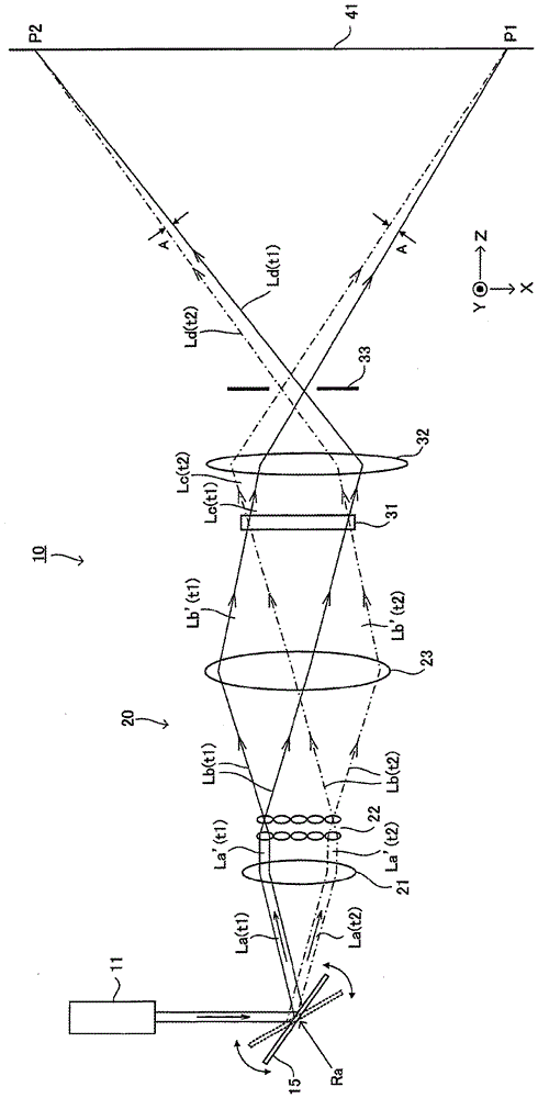
本实施方式的投射型影像显示装置10具备照明装置20、用于形成影像的光调制元件31以及将由光调制元件31形成的影像投射至屏幕41的投射光学系统32等。此外,在图中,以投影影像的屏幕41面作为X-Y平面,以与该平面正交的轴作为Z轴。在屏幕41中,还能够使用观察由屏幕41反射的影像的反射型屏幕或观察透射屏幕41的影像的透射型屏幕任一个。The projection-type
本实施方式的照明装置20具有光源11、光扫射部15、第1光路变换系统21、透镜阵列22以及第2光路变换系统23而构成。此外,在该实施方式的照明系统20中,由除了光源11以外的其他构成构成本发明中所说的光学装置。但是,关于第1光路变换系统21,不是必须的构成。The illuminating
光源11使用射出作为相干光的激光的半导体激光器装置等各种激光器装置。从光源11射出的相干光对光扫射部15进行照明。此外,优选预先针对从光源11射出的相干光而设置谋求其截面方向的强度分布的均匀化的光束成型单元。作为设计示例,通过在光扫射部附近的面设置光束成型单元,以实现均匀化,并且,将该面与光调制元件面共轭地设定,从而能够以均匀的强度对被照明区域进行照明。As the
光扫射部15是使由光源11射出的相干光的方向随时间而变化的光学元件。在本实施方式中,使用能够使反射面以转动中心Ra为中心而转动的振镜。此外,作为使可动镜机械地转动的可动式镜器件,还考虑使用多面镜、MEMS扫描仪。另外,不限于可动式镜器件,也可以使用通过电气地变更衍射条件而使出射方向变化的可变衍射型元件或相位调制元件。在这样的元件中,由于与可动式镜器件不同,不具有可动部,因而能够减轻制造时或维护时等的工序负担。后面对详细情况进行说明。The
本实施方式的光扫射部15沿Y轴方向具有转动中心Ra,进行在X-Z面内扫射相干光的一维的扫射,但利用光扫射部15进行的相干光的扫射也可以利用一维的、二维的扫射的任一个。在任一个情况下,都需要扫射透镜阵列22的入射面,结果,能够充分地对被照明区域进行照明。The
从光源11入射的相干光通过该光扫射部15而成为方向随时间而变化的扫射光La,经过第1光路变换系统21,入射至透镜阵列22。在图中,示出最外端附近的扫射光La(t1)和La(t2)的情况,但实际上,扫射光La在该La(t1)和La(t2)之间连续地移动。The coherent light incident from the
第1光路变换系统21是进行变换以使得来自扫射部15的扫射光La相对于透镜阵列22的入射面而大致垂直地入射的光学元件,使用具有聚光功能的凸透镜等而构成。通过使这样变换的扫射光La’相对于构成透镜阵列22的各单元透镜而垂直地入射,从而使扫射光La’相对于各单元透镜在相同的条件下入射。因此,使透镜阵列22的各单元透镜的设计相同等,能够削减设计上的负担。此外,不一定必须设置该第1光路变换系统21,能够通过根据入射光的状态而变更构成透镜阵列22的单元透镜或此后的光学系统等来应对。The first optical
透镜阵列22是多个单元透镜排列在光扫射部15进行的光的扫射位置(X-Y面上)的光学元件,将入射至各单元透镜的扫射光La’变换成发散光Lb。构成透镜阵列22的单元透镜的大小、形状,能够根据需要而适当设定,例如,也可以使用作为单元透镜的形状而使用柱面透镜的柱面透镜阵列或使用由极小的大小的单元透镜构成的微透镜阵列。而且,在本实施方式中,采取各单元透镜沿光轴方向(Z轴方向)排列多级(2级)的构成。从光源11射出的相干光,不一定限于作为平行光而射出,有时候含有从平行的状态偏离一些的散射成分。在本实施方式中,通过沿光轴方向配置多级单元透镜,从而可谋求该散射成分的抑制。沿光轴方向排列的单元透镜,具有同等的直径,并且,使其中心轴沿光的前进方向一致地排列。此外,透镜阵列22也可以使用各单元透镜沿光轴方向以1级构成的方式的透镜阵列。The
第2光路变换系统23(本发明中的“光路变换系统”)是利用从透镜阵列22射出的发散光Lb对作为被照明区域的像形成区域进行照明的光学元件。从被光扫射部15进行光扫射的透镜阵列22的各点射出的发散光Lb以经过该第2光路变换系统23并随着时间经过而反复的方式对被照明区域进行照明。该第2光路变换系统23优选具有从透镜阵列22射出的发散光Lb对作为被照明区域的光调制元件31的像形成区域进行照明的聚光功能。通过抑制由透镜阵列22发散的发散光Lb的发散角度,聚光于像形成区域,从而可谋求光的利用效率的提高。而且,第2光路变换系统23优选以发散光Lb成为平行光或大致平行光的方式变换。通过作为平行光或大致平行光而对像形成区域进行照明,从而能够在大致相同的条件下对像形成区域的各区域进行照明,例如,能够均匀对像形成区域整体进行照明。The second optical path conversion system 23 (“optical path conversion system” in the present invention) is an optical element that illuminates an image forming area, which is an illuminated area, with the divergent light Lb emitted from the
此外,作为第2光路变换系统23,具有抑制发散角度的功能即可,使用透镜或凹面镜、反射镜或棱镜的组合等。也可以由具有同等的功能的全息元件或衍射元件等实现。另外,也可以由这些的组合实现。In addition, as the second optical
另外,从第2光路变换系统23射出的发散光Lb’,在各时刻,对像形成区域的至少一部分进行照明,通过利用光扫射部15的扫射对像形成区域整体进行照明即可,但优选发散光Lb’在各时刻对像形成区域整体进行照明。依据这样的构成,能够谋求像形成区域的辉度分布的均匀化。In addition, the divergent light Lb' emitted from the second optical
光调制元件31是具有基于影像信号而形成像的像形成区域的显示器,在本实施方式中,使用透射型的液晶显示元件。作为光调制元件31,除了这样的透射型的元件以外,还能够利用MEMS等反射型的元件。来自第2光路变换系统23的发散光Lb’,伴随着时间的经过而使入射角度变化的同时,入射至光调制元件31,基于显示于像形成区域的像而变换成调制光Lc。The
投射光学系统32将来自光调制元件31的调制光Lc放大变换成影像再现光Ld并投射至屏幕41。在本实施方式中,在该投射光学系统32的后级设有光阑33。优选将该光阑33(投射光学系统的光瞳面)与透镜阵列的各单元透镜的焦平面保持为大致共轭。通过该构成,从而对于来自全部的单元透镜的光束,能够使成像的光学特性在光调制元件的面内均匀。The projection
那么,在该投射型影像显示装置10中,对作为用于抑制斑点的主要构成的照明装置20详细地说明其原理等。图2是示出本发明的实施方式所涉及的照明装置20的构成的图,是示出透镜阵列22导致的照明的情况的图。Then, in the projection type
如图2所示,时刻t1时的扫射光La(t1)在由第1光路变换系统21变换为相对于透镜阵列22的入射面而垂直地入射之后,入射至透镜阵列22,并射出发散光Lb(t1)。从透镜阵列22射出的发散光Lb(t1)在由第2光路变换系统23变换为对光调制元件31的像形成区域的至少一部分的区域进行照明之后,对该区域进行照明。时刻t2时的扫射光La(t2)也同样地,在变换为从第2光路变换系统23射出的发散光Lb’(t2)之后,对像形成区域的至少一部分的区域进行照明。如该图所示,照明装置20一边使相对于被照明区域的入射角度随时间而变化,一边进行照明。As shown in FIG. 2 , after the scanning light La ( t1 ) at time t1 is converted by the first optical
返回至图1,使观察者观察由光调制元件31调制的调制光Lc被投射光学系统32放大并作为影像再现光Ld而投射至屏幕41上并反射或透射而成的影像。此时,投射至屏幕41的面上的相干光互相干涉,由此,产生斑点。然而,在本实施方式中,由于由光扫射部15扫射相干光,因而结果使投射至屏幕41的影像再现光Ld的入射角度随着时间经过而变化,极其有效地使该斑点不明显。Returning to FIG. 1 , the observer is allowed to observe an image in which the modulated light Lc modulated by the
在图1所示的屏幕上的点P1,例如,时刻t1的影像再现光Ld(t1)和时刻t2的影像再现光Ld(t2)以不同的入射角度照射。在图示的另一点P2和未图示的其他点也是如此,影像再现光Ld一边使入射角度随时间而变化,一边将影像投射至屏幕41上。因此,影像再现光Ld以随时间而不同的入射角度照射,由此,在视觉的响应时间内随时间而平均化,在极短的时间内形成于屏幕上的斑点成为对观察投射至屏幕41的像的观察者充分地不明显的状态。At the point P1 on the screen shown in FIG. 1 , for example, the image reproduction light Ld(t1) at time t1 and the image reproduction light Ld(t2) at time t2 are irradiated at different incident angles. Also at the other point P2 shown in the figure and other points not shown in the figure, the image reproduction light Ld projects the image on the
在由观察者观察的斑点中,不但存在这样地由于屏幕41上的相干光的散射而产生的斑点,而且还存在在投射型影像显示装置10的各种光学元件上产生的斑点。该斑点经由光调制元件31而投影至屏幕41,由此被观察者观察。在本实施方式中,扫射光La扫射透镜阵列22,由此,对作为被照明区域的光调制元件31的像形成区域进行照明。即,通过以来自透镜阵列22的各点的发散光在时间上分离的方式对被照明区域进行照明,从而还能够消除比透镜阵列22更超前的相位信息并防止来自透镜阵列22的各点的发散光彼此干涉,能够使由投射型影像显示装置10的各种光学元件产生的斑点成为充分地不明显的状态。Among the speckles observed by the observer, there are not only speckles generated by scattering of coherent light on the
这样,在本实施方式中,利用光扫射部15导致的扫射光La’使位置随时间而变化并扫射透镜阵列22。由于透镜阵列22由邻接的多个单元透镜构成,因而有时候入射的光束跨越邻接的单元透镜而照射。此时,考虑从各单元透镜射出的出射光干涉而在被照明区域产生不均匀或条纹模样等不良。In this way, in the present embodiment, the
为了抑制这样的各单元透镜的出射光的干涉,优选采取如以下那样的构成。图3是示出本发明的实施方式所涉及的透镜阵列22与入射至透镜阵列22的扫射光La’的关系的图。在图中,示出扫射光La’的光束跨越构成透镜阵列22的2个单元透镜231a、231b而入射的状态。如该图所示,扫射光La’通过各单元透镜231a、231b而成为发散光Lb_1、Lb_2并对光调制元件31进行照明。此时,作为条件,预先设定为扫射光La’的光束宽度d1比邻接的单元透镜间隔d2更小,由此,不使各发散光Lb_1、Lb_2叠加,能够抑制各发散光Lb_1、Lb_2的干涉。In order to suppress such interference of light emitted from the unit lenses, it is preferable to adopt the following configuration. FIG. 3 is a diagram showing the relationship between the
作为防止各单元透镜231的出射光的干涉的手段,除了这样地规定光束宽度d1与单元透镜间隔d2的关系以外,还考虑采取如以下那样的构成。图4是示出本发明的另一实施方式所涉及的用于防止单元透镜间的干涉的构成的图。As means for preventing the interference of the light emitted from the unit lenses 231 , in addition to defining the relationship between the beam width d1 and the unit lens interval d2 as described above, the following configuration can be considered. 4 is a diagram showing a configuration for preventing interference between unit lenses according to another embodiment of the present invention.
图4(a)是在构成透镜阵列22的单元透镜231的前级每隔1个而配置作为设置光程差的光学元件的透明体232的实施方式。依据这样的构成,通过使邻接的单元透镜231、例如231a与231b之间的光程相差光源的相干长以上,从而能够防止各单元透镜231的出射光的干涉。FIG. 4( a ) is an embodiment in which transparent bodies 232 serving as optical elements for providing optical path differences are disposed at every other stage before the unit lenses 231 constituting the
图4(b)是在构成透镜阵列22的单元透镜231的前级配设有λ/4波片233的实施方式。如图所示,邻接的λ/4波片233、例如233a和233b配设为偏振光方向不同。另外,入射光预先设定为直线偏振光状态。通过这样的构成,从而也能够防止从各单元透镜231射出的出射光的干涉。在该示例中,来自单元透镜231的出射光是圆偏振光,关于邻接的单元透镜231,通过由λ/4波片233使其为右旋转或左旋转而不同,从而可谋求干涉的防止。或者,也可以将入射光设定为各向同性的偏振光状态并在单元透镜的前级设置使轴方向不同的偏振光板。另外,也可以使用这些以外的构成的将偏振光状态变化为不干涉的状态的元件。FIG. 4( b ) shows an embodiment in which a λ/4 wave plate 233 is disposed in the front stage of the unit lens 231 constituting the
在图4(a)中说明的透明体232、在图4(b)中说明的λ/4波片233,即使代替配置于单元透镜231的前级而配置于后级,也能得到同样的效果。另外,也可以将在图3中说明的实施方式的构成、在图4中说明的实施方式的各构成并用。Even if the transparent body 232 illustrated in FIG. 4( a ) and the λ/4 wave plate 233 illustrated in FIG. 4( b ) are arranged in the rear stage instead of the front stage of the unit lens 231 , the same can be obtained. Effect. In addition, the configuration of the embodiment described in FIG. 3 and each configuration of the embodiment described in FIG. 4 may be used in combination.
另外,在本实施方式中使用的透镜阵列22,关于构成该透镜阵列22的单元透镜231,也可以使用折射率分布型的透镜。图5是示出利用折射率分布型透镜的透镜阵列的构成的图。折射率分布型透镜是按每个构成透镜的区域,通过使材质等不同等而使折射率不同的透镜。特别地,在像本实施方式那样的扫射入射面的方式中,能够使与入射角度等入射光的各种条件相应地进行的单元透镜231的设计变得容易。在图5中,关于透镜阵列22的一部分,将所排列的折射率分布型的单元透镜231与光轴中心、光路的情况一起示出。In addition, as the
另外,关于光扫射部15,在图1中,对使用振镜的可动式镜器件进行了说明,但还能够使用不具有可动部的可变衍射型元件或相位调制元件。图6是示出本发明的另一实施方式所涉及的光扫射部(可变衍射型元件)的构成的图,图7是示出本发明的另一实施方式所涉及的光扫射部(相位调制元件)的构成和相位变化的情况的图,图8是示出本发明的另一实施方式所涉及的光扫射部(相位调制元件)中的相位变化的情况的图。In addition, as for the
图6的光扫射部15是利用可变衍射型元件的实施方式,在该实施方式中,作为可变衍射型元件而利用振幅调制型的液晶元件。构成光扫射部15的液晶元件由液晶151形成衍射光栅。通过使由该液晶151形成的衍射光栅的间距随时间变化而改变衍射角度,从而能够使从光源11入射的相干光的出射方向随时间而变化。在本实施方式中,通过使相干光相对于光扫射部15的入射面而倾斜地入射,从而能够放过0级光并使衍射光沿元件的法线方向射出。The
作为可变衍射型元件,除了该液晶元件以外,也可以使用声光学元件等调制所通过的光的相位的光学元件。或者,还能够使用对反射的光调制相位的微镜器件。As the variable diffractive element, in addition to the liquid crystal element, an optical element that modulates the phase of light passing through, such as an acousto-optical element, may be used. Alternatively, micromirror devices that modulate the phase of the reflected light can also be used.
图7的光扫射部15是利用相位调制元件的实施方式,在该实施方式中,利用仅进行相位的调制的液晶元件。图7(a)是示出该构成示例的图,光扫射部15具有封入透明基体材料153、154之间的液晶层152而构成。在液晶层152,设有按每个部分而配设的像素电极152a和共用电极152b,通过按每个部分使折射率随着时间经过而变化,从而能够使透射光的相位变化。The
图7(b)是示出相位变化的基本型的图,以与图7(a)的构成图相对应的形状示出相位分布。通过使施加至像素电极152a的偏压随时间而变化,从而能够形成例如如时刻t1、t2所示的相位分布。在这样的相位分布中,如图7(a)所示,能够偏转为在时刻t1为扫射光La(t1)而在时刻t2为扫射光La(t2)的状态。实际上,通过在t1的相位状态与t2的相位状间多阶段或连续地变化,从而关于扫射光La,也能够使方向多阶段或连续地变化。FIG.7(b) is a figure which shows the basic form of a phase change, and shows the phase distribution in the shape corresponding to the structure diagram of FIG.7(a). By changing the bias voltage applied to the
图8是示出相位变化的另一方式的图,将相位分布设为基诺全息照片型,即,使以0~2π重复的图案随时间而变更,由此,使偏转条件随时间而变更,与图7(b)的情况同样地使偏转方向变化。该图与图7(b)同样地以与图7(a)的构成图相对应的形状示出相位分布,图8(a)示出时刻t1的相位状态,图8(e)示出时刻t2的相位状态。通过使图8(a)至图8(e)、图8(e)至图8(a)之间的相位形状随着时间经过而变化,从而使从光源11入射的相干光成为偏振光。此外,相位分布也可以使用设定为0~2π以外的范围的菲涅耳透镜型。FIG. 8 is a diagram showing another form of phase change, in which the phase distribution is a Keno hologram type, that is, a pattern repeating 0 to 2π is changed with time, thereby changing the deflection condition with time, The deflection direction is changed in the same manner as in the case of FIG. 7( b ). This figure shows the phase distribution in a shape corresponding to the configuration diagram of FIG. 7( a ) as in FIG. 7( b ), FIG. 8( a ) shows the phase state at time t1 , and FIG. 8( e ) shows the time Phase state of t2. By changing the phase shape between FIGS. 8( a ) to 8( e ) and FIGS. 8( e ) to 8( a ) with time, the coherent light incident from the
在这样地在光扫射部15利用相位调制元件的情况下,由于与利用前述的可变衍射型元件的情况不同,不产生0级光,因而可谋求光的利用效率的提高。另外,如图所示,还能够使相干光相对于光扫射部15的入射面而垂直地入射。When the phase modulation element is used in the
以上,依据本实施方式,能够提供使斑点干扰不明显的照明装置以及能够通过由该照明装置对光调制元件31进行照明而提供斑点干扰不明显的影像的投射型影像显示装置。特别地,在本实施方式中,通过将由透镜阵列22发散的发散光经由第2光路变换系统23而进行照明,从而可谋求光的利用效率提高。As described above, according to the present embodiment, it is possible to provide an illumination device in which speckle disturbance is inconspicuous, and a projection-type image display device capable of providing an image in which speckle disturbance is inconspicuous by illuminating the
此外,本发明不仅仅限于这些实施方式,将各个实施方式的构成适当组合而构成的实施方式也成为本发明的范畴。In addition, the present invention is not limited to these embodiments, and an embodiment configured by appropriately combining the configurations of the respective embodiments also falls within the scope of the present invention.
附图标记说明Description of reference numerals
10……投射型影像显示装置10...Projection type image display device
11……光源11...Light source
15……光扫射部15...Light scanning section
151……液晶151...LCD
152……液晶层152...Liquid crystal layer
152a……像素电极152a...pixel electrode
152b……共用电极152b...Common electrode
153、154……透明基体材料153, 154...Transparent base material
21……第1光路变换系统21...The first optical path conversion system
22……透镜阵列22...Lens array
23……第2光路变换系统23...The second optical path conversion system
231……单元透镜231...Unit Lens
232……光学元件(透明体)232...optical element (transparent body)
233……λ/4波片。233...λ/4 wave plate.
Claims (13)
Applications Claiming Priority (3)
| Application Number | Priority Date | Filing Date | Title |
|---|---|---|---|
| JP2011105456A JP5168526B2 (en) | 2011-05-10 | 2011-05-10 | Projection-type image display device |
| JP2011-105456 | 2011-05-10 | ||
| CN201280022332.9A CN103502887A (en) | 2011-05-10 | 2012-04-23 | Illumination device, projection type image display device and optical device |
Related Parent Applications (1)
| Application Number | Title | Priority Date | Filing Date |
|---|---|---|---|
| CN201280022332.9A Division CN103502887A (en) | 2011-05-10 | 2012-04-23 | Illumination device, projection type image display device and optical device |
Publications (2)
| Publication Number | Publication Date |
|---|---|
| CN107577112A CN107577112A (en) | 2018-01-12 |
| CN107577112B true CN107577112B (en) | 2020-10-23 |
Family
ID=47139112
Family Applications (2)
| Application Number | Title | Priority Date | Filing Date |
|---|---|---|---|
| CN201280022332.9A Pending CN103502887A (en) | 2011-05-10 | 2012-04-23 | Illumination device, projection type image display device and optical device |
| CN201710907452.1A Active CN107577112B (en) | 2011-05-10 | 2012-04-23 | Illumination device, projection type image display device, and optical device |
Family Applications Before (1)
| Application Number | Title | Priority Date | Filing Date |
|---|---|---|---|
| CN201280022332.9A Pending CN103502887A (en) | 2011-05-10 | 2012-04-23 | Illumination device, projection type image display device and optical device |
Country Status (5)
| Country | Link |
|---|---|
| US (2) | US8992029B2 (en) |
| EP (2) | EP2708948B1 (en) |
| JP (1) | JP5168526B2 (en) |
| CN (2) | CN103502887A (en) |
| WO (1) | WO2012153626A1 (en) |
Families Citing this family (33)
| Publication number | Priority date | Publication date | Assignee | Title |
|---|---|---|---|---|
| JP5541462B2 (en) | 2011-05-10 | 2014-07-09 | 大日本印刷株式会社 | Projection-type image display device |
| JP5849727B2 (en) * | 2012-01-26 | 2016-02-03 | 株式会社Jvcケンウッド | Projection display |
| JP5849728B2 (en) * | 2012-01-26 | 2016-02-03 | 株式会社Jvcケンウッド | Projection display |
| JP6131736B2 (en) * | 2013-06-25 | 2017-05-24 | 大日本印刷株式会社 | Projection device and projection display device |
| KR101399971B1 (en) * | 2013-09-13 | 2014-06-27 | (주)엘투케이플러스 | Apparatus adjusting the focal point position of laser beam |
| JP2015099323A (en) * | 2013-11-20 | 2015-05-28 | セイコーエプソン株式会社 | projector |
| JP6252298B2 (en) * | 2014-03-27 | 2017-12-27 | 大日本印刷株式会社 | Lighting device |
| JP6331826B2 (en) * | 2014-07-23 | 2018-05-30 | 大日本印刷株式会社 | Projection device and lighting device |
| TWI617841B (en) * | 2014-10-22 | 2018-03-11 | 英特爾股份有限公司 | Anti-moire pattern diffuser for optical systems |
| JP6507606B2 (en) * | 2014-12-05 | 2019-05-08 | 大日本印刷株式会社 | Underwater lighting device |
| US10941915B2 (en) * | 2015-09-07 | 2021-03-09 | Dai Nippon Printing Co., Ltd. | Illumination device for illuminating a predetermined range with coherent light |
| CN108291703B (en) * | 2015-11-20 | 2020-12-29 | 大日本印刷株式会社 | Lighting device |
| JP6700579B2 (en) * | 2015-12-04 | 2020-05-27 | 大日本印刷株式会社 | Variable speckle generator |
| DE102015224880A1 (en) * | 2015-12-10 | 2017-06-14 | Osram Gmbh | Headlamp for lighting |
| CN107102503A (en) * | 2016-02-19 | 2017-08-29 | 中国科学院苏州纳米技术与纳米仿生研究所 | Eliminate the light-source system and projection arrangement of laser speckle |
| WO2018025506A1 (en) * | 2016-08-02 | 2018-02-08 | ソニー株式会社 | Projection-type display apparatus |
| JP6471840B2 (en) * | 2016-11-17 | 2019-02-20 | 大日本印刷株式会社 | Lighting device |
| JP6761600B2 (en) | 2017-01-05 | 2020-09-30 | 大日本印刷株式会社 | Lighting device |
| JP6926526B2 (en) | 2017-02-28 | 2021-08-25 | セイコーエプソン株式会社 | projector |
| KR102449093B1 (en) * | 2017-03-24 | 2022-09-29 | 삼성디스플레이 주식회사 | display device |
| JP6332516B2 (en) * | 2017-04-12 | 2018-05-30 | 大日本印刷株式会社 | Projection device and projection display device |
| JP7053227B2 (en) * | 2017-11-16 | 2022-04-12 | スタンレー電気株式会社 | Light irradiation device and vehicle lighting equipment |
| EP3732529B1 (en) | 2017-12-28 | 2024-02-28 | AMS Sensors Singapore Pte. Ltd. | Light-emitting optoelectronic modules |
| JP7087828B2 (en) * | 2018-08-27 | 2022-06-21 | セイコーエプソン株式会社 | Optical elements, light emitting devices and image display systems |
| JP7417874B2 (en) * | 2019-06-28 | 2024-01-19 | 大日本印刷株式会社 | Lighting device and lighting method |
| CN110275313A (en) * | 2019-07-24 | 2019-09-24 | 山西大学 | A static speckle suppression device and laser projection display system |
| TWI859179B (en) * | 2020-01-06 | 2024-10-21 | 揚明光學股份有限公司 | Projection device, headlight for vehicle and manufacturing method thereof |
| CN113495419B (en) * | 2020-04-07 | 2025-08-08 | 深圳光峰科技股份有限公司 | Light source system and projection display device |
| CN114185232A (en) * | 2020-09-14 | 2022-03-15 | 深圳光峰科技股份有限公司 | Display device |
| JP2022160182A (en) * | 2021-04-06 | 2022-10-19 | 株式会社日立エルジーデータストレージ | Optical unit, and head-mounted display device using the same |
| JP7748617B2 (en) * | 2021-09-03 | 2025-10-03 | 大日本印刷株式会社 | Projection display device and working device |
| DE102021130561A1 (en) * | 2021-11-23 | 2023-05-25 | Carl Zeiss Jena Gmbh | PROJECTOR OR DISPLAY WITH SCANNING LIGHT SOURCE AND PIXELATED ARRAY |
| JP2023131646A (en) * | 2022-03-09 | 2023-09-22 | 株式会社リコー | Light source device and display device |
Citations (9)
| Publication number | Priority date | Publication date | Assignee | Title |
|---|---|---|---|---|
| CN1894624A (en) * | 2003-12-24 | 2007-01-10 | 松下电器产业株式会社 | 2-dimensional image display device |
| CN1982946A (en) * | 2005-12-14 | 2007-06-20 | 三星电子株式会社 | Laser display apparatus |
| CN101093284A (en) * | 2006-06-20 | 2007-12-26 | 三星电子株式会社 | Display apparatus using laser and method of using the same |
| CN101198893A (en) * | 2005-05-17 | 2008-06-11 | 讯宝科技公司 | Image projection screen with reduced speckle noise |
| KR20090114645A (en) * | 2008-04-30 | 2009-11-04 | 엘지전자 주식회사 | Laser projection device |
| CN101595737A (en) * | 2007-01-24 | 2009-12-02 | 奥斯兰姆有限公司 | optoelectronic device |
| CN101661214A (en) * | 2008-08-27 | 2010-03-03 | 鸿富锦精密工业(深圳)有限公司 | Projector |
| CN101681078A (en) * | 2008-02-20 | 2010-03-24 | 松下电器产业株式会社 | Light source device, lighting device and image display device |
| CN201622390U (en) * | 2010-01-20 | 2010-11-03 | 安徽华东光电技术研究所 | Laser projection display system |
Family Cites Families (27)
| Publication number | Priority date | Publication date | Assignee | Title |
|---|---|---|---|---|
| JPS61212816A (en) * | 1985-03-18 | 1986-09-20 | Canon Inc | lighting equipment |
| DE3877829T2 (en) * | 1987-06-01 | 1993-07-29 | Sar Realisations Ltd | PRESENTATION SYSTEM WITH TRANSPARENT SCREEN AND METHOD FOR THE PRODUCTION THEREOF. |
| US5313479A (en) | 1992-07-29 | 1994-05-17 | Texas Instruments Incorporated | Speckle-free display system using coherent light |
| US5684566A (en) | 1995-05-24 | 1997-11-04 | Svg Lithography Systems, Inc. | Illumination system and method employing a deformable mirror and diffractive optical elements |
| US5923475A (en) * | 1996-11-27 | 1999-07-13 | Eastman Kodak Company | Laser printer using a fly's eye integrator |
| GB9709926D0 (en) * | 1997-05-15 | 1997-07-09 | Screen Tech Ltd | Liquid-crystal display |
| US6800859B1 (en) * | 1998-12-28 | 2004-10-05 | Hitachi, Ltd. | Method and equipment for detecting pattern defect |
| JP2002244069A (en) * | 2001-02-19 | 2002-08-28 | Nec Corp | Laser scanning optical device and laser scanning method using this optical device |
| US6577429B1 (en) * | 2002-01-15 | 2003-06-10 | Eastman Kodak Company | Laser projection display system |
| JP4084203B2 (en) * | 2002-01-31 | 2008-04-30 | シチズンホールディングス株式会社 | Optical deflection device |
| JP4042558B2 (en) * | 2002-12-13 | 2008-02-06 | セイコーエプソン株式会社 | projector |
| JP4291230B2 (en) * | 2004-08-06 | 2009-07-08 | 株式会社日本製鋼所 | Method and apparatus for forming crystallized film |
| WO2006137326A1 (en) * | 2005-06-20 | 2006-12-28 | Matsushita Electric Industrial Co., Ltd. | 2-dimensional image display device, illumination light source, and exposure illumination device |
| JP4701030B2 (en) * | 2005-07-22 | 2011-06-15 | キヤノン株式会社 | Exposure apparatus, setting method for setting exposure parameters, exposure method, device manufacturing method, and program |
| KR20070070930A (en) * | 2005-12-29 | 2007-07-04 | 삼성전기주식회사 | Laser projection display |
| JP4478670B2 (en) * | 2006-09-08 | 2010-06-09 | ソニー株式会社 | One-dimensional illumination device and image generation device |
| JP2008204570A (en) * | 2007-02-21 | 2008-09-04 | Ricoh Opt Ind Co Ltd | Information recording device and its light source device |
| EP1976303A1 (en) * | 2007-03-31 | 2008-10-01 | Sony Deutschland Gmbh | Image generating apparatus |
| JP4379482B2 (en) | 2007-04-03 | 2009-12-09 | セイコーエプソン株式会社 | Light source device and projector |
| JP4999583B2 (en) * | 2007-07-18 | 2012-08-15 | キヤノン株式会社 | Optical scanning device and scanning image display device |
| JP5075595B2 (en) * | 2007-11-26 | 2012-11-21 | 株式会社東芝 | Display device and moving body using the same |
| JP5386821B2 (en) * | 2007-12-28 | 2014-01-15 | セイコーエプソン株式会社 | Light source device and projector |
| CN101755300B (en) | 2008-05-21 | 2014-02-05 | 松下电器产业株式会社 | Projector |
| US7944598B2 (en) | 2008-11-06 | 2011-05-17 | Corning Incorporated | Speckle mitigation in laser scanner projector systems |
| US8113662B2 (en) * | 2009-01-22 | 2012-02-14 | Texas Instruments Incorporated | System and method for reducing the effect of an image artifact |
| US20100232005A1 (en) * | 2009-03-12 | 2010-09-16 | Microvision, Inc. | Speckle Reduction in Display Systems Using Transverse Phase Modulation in A Non-Image Plane |
| US7940448B2 (en) * | 2009-06-11 | 2011-05-10 | Alces Technology, Inc. | Display system |
-
2011
- 2011-05-10 JP JP2011105456A patent/JP5168526B2/en active Active
-
2012
- 2012-04-23 CN CN201280022332.9A patent/CN103502887A/en active Pending
- 2012-04-23 EP EP12782132.0A patent/EP2708948B1/en active Active
- 2012-04-23 US US14/115,727 patent/US8992029B2/en active Active
- 2012-04-23 CN CN201710907452.1A patent/CN107577112B/en active Active
- 2012-04-23 EP EP17199136.7A patent/EP3312670B1/en active Active
- 2012-04-23 WO PCT/JP2012/060874 patent/WO2012153626A1/en not_active Ceased
-
2015
- 2015-02-19 US US14/626,778 patent/US9609294B2/en active Active
Patent Citations (9)
| Publication number | Priority date | Publication date | Assignee | Title |
|---|---|---|---|---|
| CN1894624A (en) * | 2003-12-24 | 2007-01-10 | 松下电器产业株式会社 | 2-dimensional image display device |
| CN101198893A (en) * | 2005-05-17 | 2008-06-11 | 讯宝科技公司 | Image projection screen with reduced speckle noise |
| CN1982946A (en) * | 2005-12-14 | 2007-06-20 | 三星电子株式会社 | Laser display apparatus |
| CN101093284A (en) * | 2006-06-20 | 2007-12-26 | 三星电子株式会社 | Display apparatus using laser and method of using the same |
| CN101595737A (en) * | 2007-01-24 | 2009-12-02 | 奥斯兰姆有限公司 | optoelectronic device |
| CN101681078A (en) * | 2008-02-20 | 2010-03-24 | 松下电器产业株式会社 | Light source device, lighting device and image display device |
| KR20090114645A (en) * | 2008-04-30 | 2009-11-04 | 엘지전자 주식회사 | Laser projection device |
| CN101661214A (en) * | 2008-08-27 | 2010-03-03 | 鸿富锦精密工业(深圳)有限公司 | Projector |
| CN201622390U (en) * | 2010-01-20 | 2010-11-03 | 安徽华东光电技术研究所 | Laser projection display system |
Non-Patent Citations (1)
| Title |
|---|
| 激光显示中散斑的抑制;郝丽等;《激光与红外》;20061031;第36卷(第10期);第927-930页 * |
Also Published As
| Publication number | Publication date |
|---|---|
| CN107577112A (en) | 2018-01-12 |
| EP2708948B1 (en) | 2017-11-08 |
| CN103502887A (en) | 2014-01-08 |
| EP3312670A1 (en) | 2018-04-25 |
| EP3312670B1 (en) | 2022-03-09 |
| JP5168526B2 (en) | 2013-03-21 |
| EP2708948A1 (en) | 2014-03-19 |
| US20150163467A1 (en) | 2015-06-11 |
| JP2012237813A (en) | 2012-12-06 |
| US20140118702A1 (en) | 2014-05-01 |
| WO2012153626A1 (en) | 2012-11-15 |
| EP2708948A4 (en) | 2015-04-15 |
| US9609294B2 (en) | 2017-03-28 |
| US8992029B2 (en) | 2015-03-31 |
Similar Documents
| Publication | Publication Date | Title |
|---|---|---|
| CN107577112B (en) | Illumination device, projection type image display device, and optical device | |
| CN103797414B (en) | Illumination device, projection type image display device and optical device | |
| CN103518161B (en) | Projection device and projection control device | |
| US10365498B2 (en) | Illumination device, projection apparatus and projection-type image display apparatus | |
| JP5207013B2 (en) | Illumination device and optical device | |
| JP5804245B2 (en) | Scanning display device | |
| JP6308355B2 (en) | LIGHTING DEVICE, PROJECTION VIDEO DISPLAY DEVICE, OPTICAL DEVICE, AND OPTICAL ELEMENT | |
| JP5783359B2 (en) | Illumination device and projection-type image display device | |
| JP6460182B2 (en) | Illumination device and light deflection device | |
| JP6198151B2 (en) | Illumination device and light deflection device | |
| JP5794442B2 (en) | Projection-type image display device |
Legal Events
| Date | Code | Title | Description |
|---|---|---|---|
| PB01 | Publication | ||
| PB01 | Publication | ||
| SE01 | Entry into force of request for substantive examination | ||
| SE01 | Entry into force of request for substantive examination | ||
| GR01 | Patent grant | ||
| GR01 | Patent grant |