Detailed Description
I. General considerations
The present disclosure is set forth in the context of representative embodiments that are not intended to be limiting in any way.
As used in this application, the singular forms "a", "an" and "the" include plural referents unless the context clearly dictates otherwise. Additionally, the term "comprising" means "including". Further, the term "coupled" encompasses mechanical, electrical, magnetic, optical, and other practical ways of coupling or linking items together, and does not exclude the presence of intermediate elements between coupled items. Still further, as used herein, the term "and/or" refers to any one or combination of multiple items in the phrase.
The systems, methods, and apparatus described herein should not be construed as limiting in any way. Rather, the present disclosure is directed to all novel and non-obvious features and aspects of the various disclosed embodiments, alone and in various combinations and sub-combinations with each other. The disclosed systems, methods, and apparatus are not limited to any specific aspect or feature or combination thereof, nor do the disclosed subject matter and methods require that any one or more specific advantages be present or problems be solved. Further, any features or aspects of the disclosed embodiments can be used in various combinations and sub-combinations with each other.
Although the operations of some of the disclosed methods are described in a particular, sequential order for convenient presentation, it should be understood that this manner of description encompasses rearrangement, unless a particular ordering is required by specific language set forth below. For example, operations described sequentially may in some cases be rearranged or performed in parallel. Moreover, for the sake of simplicity, the attached figures may not show the various ways in which the disclosed content and methods can be used in conjunction with other content and methods. Additionally, terms such as "producing," "generating," "displaying," "receiving," "transmitting," "authenticating," "performing," and "initiating" are sometimes used in the specification to describe the disclosed methods. These terms are high-level descriptions of the actual operations performed. The actual operations that correspond to these terms will vary depending on the particular implementation and are readily discernible by one of ordinary skill in the art.
For purposes of better understanding, there has been provided a theoretical, scientific, or other description of the operation given herein with reference to the apparatus or methods of the present disclosure, and is not intended to be limiting in scope. The apparatus and methods in the appended claims are not limited to those apparatus and methods implemented in the manner described by these theories of operation.
Any of the disclosed methods are implemented as computer-executable instructions stored on one or more computer-readable media (e.g., computer-readable media such as one or more optical media discs, volatile memory components (such as DRAM or SRAM), or non-volatile memory components (such as hard drives)) and executed on a computer (e.g., of any commercially available computer, including smart phones or other mobile devices that include computing hardware). Any of the computer-executable instructions for implementing the disclosed techniques, as well as any data created and used during implementation of the disclosed embodiments, can be stored on one or more computer-readable media (e.g., computer-readable storage media). The computer-executable instructions may be a dedicated software application or a portion of a software application that is accessed or downloaded, for example, via a web browser or other software application, such as a remote computing application. Such software can be executed, for example, using one or more network computers, on a single local computer (e.g., with a general-purpose processor and/or a block-based processor executing on any suitable commercially-available computer) or in a network environment (e.g., via the internet, a wide-area network, a local-area network, a client-server network (such as a cloud computing network), or other such network).
For clarity, only certain selected aspects of the software-based implementation are described. Other details known in the art are omitted. For example, it should be appreciated that the disclosed technology is not limited to any particular computer language or program. For example, the disclosed techniques may be implemented by software written in C, C + +, Java, or any other suitable programming language. Likewise, the disclosed technology is not limited to any particular computer or type of hardware. Certain details of suitable computers and hardware are well known and need not be set forth in detail in this disclosure.
Still further, any of the software-based embodiments (including, for example, computer-executable instructions for causing a computer to perform any of the disclosed methods) may be uploaded, downloaded, or remotely accessed through suitable communication means. Such suitable communication means include, for example, the internet, the world wide web, an intranet, software applications, electrical cables (including fiber optic cables), magnetic communication, electromagnetic communication (including RF, microwave, and infrared communication), electronic communication, or other such communication means.
Introduction to the disclosed technology
Superscalar out-of-order micro-architectures employ a large number of circuit resources to rename registers, schedule instructions in dataflow order, clean up after mis-speculation, and retire results in order for precise exceptions. This includes expensive circuitry such as deep multiported register files, multiported Content Accessible Memory (CAM) for data stream instruction dispatch wakeup, and many wide bus multiplexers and bypass networks, all of which are resource intensive. For example, FPGA-based implementations of multiple read and write RAMs typically require a mix of replication, multi-cycle operation, clock doubling, group interleaving, live value tables, and other expensive techniques.
The disclosed techniques may achieve performance enhancement by applying techniques including high Instruction Level Parallelism (ILP), out-of-order (OoO), superscalar execution, while avoiding substantial complexity and overhead in processor hardware and related software. In some examples of the disclosed technology, block-based processors use the EDGE ISA designed for area and energy efficient ILP execution. In some examples, clever processing is used using the EDGE architecture and associated compiler, remote from register renaming, CAM, and many of the complexities.
In some examples of the disclosed technology, the EDGE ISA may eliminate the need for one or more complex architectural features including register renaming, dataflow analysis, misprediction recovery, and in-order retirement, while supporting mainstream programming languages such as C and C + +. In some examples of the disclosed technology, a block-based processor executes a plurality of two or more instructions as atomic blocks. Block-based instructions may be used to express the semantics of a program data stream and/or instruction stream in a more explicit manner, thereby improving the performance of compilers and processors. In some examples of the disclosed technology, an explicit data graph execution instruction set architecture (EDGE ISA) includes information about program control flow, which is used to improve detection of inappropriate control flow instructions, thereby improving performance, saving memory resources, and/or saving energy.
In some examples of the disclosed technology, instructions organized within instruction blocks are atomically fetched, executed, and committed. The instructions within the block execute in dataflow order, which reduces or eliminates the use of register renaming and provides power efficient OoO execution. A compiler may be used to explicitly encode data dependencies through the ISA, thereby reducing or eliminating the burden of processor core control logic to rediscover dependencies at runtime. With predicated execution, intra-block branches may be converted to dataflow instructions, and dependencies other than memory dependencies may be limited to direct data dependencies. The disclosed target form encoding techniques allow instructions within a block to communicate their operands directly via an operand buffer, thereby reducing access to power consuming multi-ported physical register files.
Between instruction blocks, instructions may communicate using memory and registers. Thus, by utilizing a mixed data stream execution model, the EDGE architecture can still support imperative programming language and sequential memory semantics, but desirably also enjoy the benefits of out-of-order execution with near-sequential power efficiency and complexity.
Apparatus, methods, and computer-readable storage media are disclosed for generating and using block-based branch metadata for block-based processors. In some examples of the disclosed technology, the instruction block includes an instruction block header and a plurality of instructions. In other words, the instructions executed by the instruction block affect the state, or do not affect the state as a unit.
In some examples of the disclosed technology, a hardware structure stores data indicating an execution order to be adhered to for a number of memory access instructions (including memory load and memory store instructions). A control unit coupled to the processor core controls issuance of the memory access instructions based at least in part on data stored in the hardware structure. Thus, memory read/write hazards may be avoided while allowing instructions in an instruction block to execute immediately when their dependencies are available.
As one of ordinary skill in the relevant art will readily appreciate, the scope of implementations of the disclosed technology may be subject to various domains and performance tradeoffs.
Example Block-based processor
Fig. 1 is a block diagram 10 of a block-based processor 100 as may be implemented in some examples of the disclosed technology. Processor 100 is configured to execute atomic instruction blocks according to an Instruction Set Architecture (ISA) that describes several aspects of processor operation, including a register model, several defined operations performed by block-based instructions, a memory model, interrupts, and other architectural features. The block-based processor includes a plurality of processing cores 110, including a processor core 111.
As shown in FIG. 1, the processor cores are connected to each other via a core interconnect 120. Core interconnect 120 passes data and control signals between various ones of cores 110, memory interface 140, and input/output (I/O) interface 145. Core interconnect 120 may transmit and receive signals using electrical, optical, magnetic, or other suitable communication techniques, and may provide communication connections arranged according to a number of different topologies, depending on the particular desired configuration. For example, core interconnect 120 may have a crossbar, bus, point-to-point bus, or other suitable topology. In some examples, any one of cores 110 may be connected to any one of the other cores, while in other examples, some cores are connected to only a subset of the other cores. For example, each core can only connect to the nearest 4, 8, or 20 neighboring cores. Core interconnect 120 may be used to transfer input/output data to and from the cores, and to transfer control signals and other information signals to and from the cores. For example, each of the cores 110 may receive and transmit a semaphore indicating the execution state of instructions currently being executed by each of the cores. In some examples, core interconnect 120 is implemented as a wire connecting core 110 and the memory system, while in other examples, the core interconnect may include circuitry for multiplexing data signals on one or more interconnect wires; and a switching and/or routing assembly comprising an active signal driver and a repeater; or other suitable circuitry. In some examples of the disclosed technology, signals communicated within processor 100 and to/from processor 100 are not limited to full-swing electrical digital signals, but rather the processor may be configured to include differential signals, pulsed signals, or other suitable signals for communicating data and control signals.
In the example of fig. 1, memory interface 140 of the processor includes interface logic that is used to connect to additional memory, e.g., memory located on another integrated circuit than processor 100. External memory system 150 includes L2 cache 152 and main memory 155. In some examples, the L2 cache may be implemented using static ram (sram), while the main memory 155 may be implemented using dynamic ram (dram). In some examples, memory system 150 is included on the same integrated circuit as the other components of processor 100. In some examples, memory interface 140 includes a Direct Memory Access (DMA) controller that allows data blocks to be transferred in memory without using one or more register files and/or processor 100. In some examples, the memory interface manages allocation of virtual memory, thereby extending the available main memory 155.
The I/O interface 145 includes circuitry to receive and transmit input and output signals from and to other components, such as hardware interrupts, system control signals, peripheral interfaces, coprocessor control and/or data signals (e.g., signals for a graphics processing unit, floating point coprocessor, physical processing unit, digital signal processor, or other co-processing component), clock signals, semaphores, or other suitable I/O signals. The I/O signals may be synchronous or asynchronous. In some examples, all or a portion of the I/O interface is implemented using memory mapped I/O techniques in conjunction with memory interface 140.
The block-based processor 100 may also include a control unit 160. Control unit 160 oversees the operation of processor 100. Operations that may be performed by the control unit 160 may include allocation and deallocation of cores for performing instruction processing; control input data and output data between any of the cores, the register file, the memory interface 140, and/or the I/O interface 145; modifying the execution flow; and verifying the target location of branch instructions, instruction headers, and other changes in control flow. The control unit 160 may generate and control the processor based on control flow and metadata information representing the exit point and control flow probabilities for the instruction blocks.
The control unit 160 may also handle hardware interrupts and control the reading and writing of special system registers (e.g., program counters stored in one or more register files). In some examples of the disclosed technology, control unit 160 is implemented at least in part using one or more of processing cores 110, while in other examples, control unit 160 is implemented using a non-block-based processing core (e.g., a general-purpose RISC processing core coupled to a memory). In some examples, control unit 160 is implemented at least in part using one or more of: a hardwired finite state machine, programmable microcode, programmable gate array, or other suitable control circuitry. In alternative examples, the control unit functions may be performed by one or more of cores 110.
The control unit 160 includes a scheduler 165 that is used to allocate instruction blocks to the processor cores 110. As used herein, scheduler block allocation refers to a pilot operation of an instruction block, which includes: initiating instruction block mapping, fetching, decoding, executing, committing, aborting, idling, and refreshing instruction blocks. Further, instruction scheduling refers to scheduling the issuance and execution of instructions within an instruction block. For example, based on instruction dependencies and data indicating relative ordering for memory access instructions, control unit 160 may determine which instruction or instructions in an instruction block are ready to issue, and initiate issuance and execution of the instructions. Processor cores 110 are assigned to instruction blocks during instruction block mapping. The instruction operation stages described are for illustration purposes, and in some examples of the disclosed technology, certain operations may be combined, omitted, split into multiple operations, or additional operations added. Scheduler 165 schedules instruction streams that include the allocation and de-allocation of cores for performing instruction processing; control input data and output data between any of the cores, the register file, the memory interface 140, and/or the I/O interface. As discussed in further detail below, the control unit 160 also includes a memory-access instruction hardware structure 167 that may be used to store data including data indicating a relative ordering for executing memory-access instructions, such as a store mask or store counter and a store vector register that stores data indicating which instructions (e.g., which load and/or store instructions) have been executed within an instruction block.
Block-based processor 100 also includes a clock generator 170 that distributes one or more clock signals to various components within the processor (e.g., cores 110, interconnects 120, memory interface 140, and I/O interface 145). In some examples of the disclosed technology, all components share a common clock, while in other examples, different components use different clocks, e.g., clock signals having different clock frequencies. In some examples, a portion of the clock is gated to allow power savings when some of the processor components are not being used. In some examples, a clock signal is generated using a phase-locked loop (PLL) to generate a signal having a fixed constant frequency and duty cycle. The circuits receiving the clock signal may be triggered on a single edge (e.g., a rising edge), while in other examples at least some of the circuits in the receiving circuit are triggered by both rising and falling clock edges. In some examples, the clock signal may be transmitted optically or wirelessly.
Block-based processor core example
Fig. 2 is a block diagram further detailing an example micro-architecture for block-based processor 100 (and in particular, an example of one of the block-based processor cores as may be used in certain examples of the disclosed technology). For ease of explanation, the exemplary block-based processor core is illustrated with five stages: instruction Fetching (IF), Decoding (DC), operand fetching, Execution (EX) and memory/data access (LS). However, one of ordinary skill in the relevant art will readily appreciate that modifications to the illustrated micro-architecture (such as addition/removal stages, addition/removal units to perform operations, and other implementation details) may be modified to adapt a particular application to a block-based processor.
As shown in fig. 2, processor core 111 includes a control unit 205 that generates control signals to regulate core operations and schedules instruction flow within the core using instruction scheduler 206. Operations that may be performed by control unit 205 and/or instruction scheduler 206 may include: generating and encoding using memory access instructions; allocating and de-allocating cores for performing instruction processing; controls input data and output data between any of the cores, the register file, the memory interface 140, and/or the I/O interface 145.
In some examples, instruction scheduler 206 is implemented using a general purpose processor coupled to a memory configured to store data for scheduling instruction blocks. In some examples, instruction scheduler 206 is implemented using a special-purpose processor or using a block-based processor core coupled to memory. In some examples, instruction scheduler 206 is implemented as a finite state machine coupled to a memory. In some examples, an operating system executing on a processor (e.g., a general purpose processor or block-based processor core) generates priority, prediction, and other data that may be used, at least in part, to schedule instruction blocks with instruction scheduler 206. As will be readily appreciated by one of ordinary skill in the relevant art, other circuit structures implemented in integrated circuits, programmable logic, or other suitable logic may be used to implement the hardware for instruction scheduler 206.
The control unit 205 also includes memory (e.g., in SRAM or registers) for storing control flow information and metadata. For example, data indicating the relative ordering of memory access instructions may be stored in a hardware structure such as store instruction data store 207. Store instruction data store 207 may store data for storing a mask (e.g., generated by copying data encoded in an instruction block or generated by an instruction decoder when decoding an instruction), store count data (e.g., data indicating a number of memory stores to be executed before a particular next instruction can issue), store counter (e.g., a counter storing data indicating a stored number of instructions that have issued or executed), store vector register (e.g., store data indicating which types of memory access instructions have been executed and what types of memory access instructions), and masked store vector register data (e.g., data generated by applying a store mask to a store vector register). In some examples, store instruction data store 207 includes a counter that tracks the number and type of memory access instructions that have been executed. In some examples, the store instruction data store 207 stores data in a table (e.g., a multidimensional table) indicating instruction identifiers, predicates, predicate paths, number of loads/stores, or other information that may be used to determine a relative ordering of execution of memory access instructions.
Instruction decoders 228 and 229 may specify the relative order for issuing and executing load and store instructions within the blocks. For example, a numerical load/store identifier (LSID) may be assigned to each memory access instruction, or only to memory store instructions. The higher numbered LSID indicates that the instruction should execute after the lower numbered LSID. In some examples, the processor may determine that the two load/store instructions do not conflict (e.g., based on the read/write address for the instructions) and may execute the instructions in a different order, although the resulting state of the machine should not be different than if the instructions had executed in the specified LSID ordering. In some examples, load/store instructions with mutually exclusive predicate values may use the same LSID value. For example, if a first load/store instruction is predicated based on the value p being true, and a second load/store instruction is predicated based on the value p being false, each instruction may have the same LSID value.
The control unit 205 may also handle hardware interrupts and control the reading and writing of special system registers (e.g., program counters stored in one or more register files). In other examples of the disclosed technology, control unit 205 and/or instruction scheduler 206 are implemented using a non-block-based processing core (e.g., a general purpose RISC processing core coupled to memory). In some examples, control unit 205 and/or instruction scheduler 206 are implemented, at least in part, using one or more of a hardwired finite state machine, programmable microcode, a programmable gate array, or other suitable control circuitry.
The exemplary processor core 111 includes two instruction windows 210 and 211, each of which may be configured to execute a block of instructions. In some examples of the disclosed technology, the instruction block is an atomic set of block-based processor instructions that includes an instruction block header and a plurality of one or more instructions. As will be discussed further below, the instruction block header includes information that may be used to further define the semantics of one or more of the plurality of instructions within the instruction block. Depending on the particular ISA and processor hardware used, instruction block headers may also be used during execution of instructions and to improve performance of executing instruction blocks by, for example, allowing early fetching of instructions and/or data, improved branch predication, speculative execution, improved energy efficiency, and improved code compactness. In other examples, different numbers of instruction windows are possible, such as one, four, eight, or other numbers of instruction windows.
Each of instruction windows 210 and 211 may receive instructions and data from one or more of input ports 220, 221 and 222 coupled to an interconnect bus and instruction cache 227, which in turn is coupled to instruction decoders 228 and 229. Additional control signals may also be received on additional input ports 225. Each of instruction decoders 228 and 229 decodes the instruction headers and/or instructions of the instruction blocks and stores the decoded instructions in memory storage 215 and 216 located in each respective instruction window 210 and 211. Further, each of decoders 228 and 229 may send data to control unit 205, for example, to configure the operation of processor core 111 according to an execution flag specified in an instruction block header or in an instruction. Each of instruction decoders 228 and 229 is configured to generate an identifier for indicating a relative ordering of one or more memory access instructions in an instruction block. These identifiers may be used to determine that all memory access instructions to be executed for the instruction block have been executed. For example, an instruction decoder may analyze an instruction (e.g., by building a control flow graph or equivalent) to determine a predicate associated with a memory access instruction in a block. Based on the predicate, it is determined that certain memory access instructions must be executed before other memory access or jump instructions in order to allow the correct instruction block to be implemented.
Processor core 111 also includes a register file 230 coupled to an LI (first level) cache 235. Register file 230 stores data for registers defined in the block-based processor architecture and may have one or more read ports and one or more write ports. For example, a register file may include two or more write ports for storing data in the register file, and have multiple read ports for reading data from various registers within the register file. In some examples, a single instruction window (e.g., instruction window 210) can only access one port of the register file at a time, while in other examples, instruction window 210 may access one read port and one write port, or may access two or more read ports and/or write ports simultaneously. In some examples, register file 230 may include 64 registers, each of which holds a word of 32-bits of data. (for ease of explanation, this application refers to 32-bit data as words unless otherwise noted. a suitable processor in accordance with the disclosed technology may operate using 8-bit words, 16-bit words, 64-bit words, 128-bit words, 256-bit words, or another digital bit word). In some examples, some of the registers within register file 230 may be allocated for special purposes. For example, some of the registers may be dedicated as system register examples, examples of which include registers that store a constant value (e.g., an all zero word), one or more Program Counters (PCs) that indicate a current address of a program thread being executed, a number of physical cores, a number of logical cores, a core allocation topology, a core control flag, an execution flag, a processor topology, or other suitable dedicated purpose. In some examples, there are multiple program counter registers, one or each program counter, to allow multiple threads of execution to be executed concurrently on one or more processor cores and/or processors. In some examples, the program counter is implemented as a specified memory location, rather than a register in a register file. In some examples, the use of system registers may be constrained by operating system or other supervisory computer instructions. In some examples, the register file 230 is implemented as a flip-flop array, while in other examples, the register file may be implemented using latches, SRAM, or other forms of memory storage. The ISA specification for a given processor (e.g., processor 100) specifies how registers within register file 230 are defined and used.
In some examples, processor 100 includes a global register file shared by multiple processor cores. In some examples, depending on the processor ISA and configuration, various register files associated with the processor cores may be combined statically or dynamically to form a larger file.
As shown in FIG. 2, the
memory storage 215 of the instruction window 210 includes a number of decoded
instructions 241, a Left Operand (LOP) buffer 242, a Right Operand (ROP) buffer 243, a
predicate buffer 244, three
broadcast channels 245, and an
instruction scoreboard 247. As shown in FIG. 2, in some examples of the disclosed technology, each instruction of an instruction block is decomposed into a line of decoded instructions, left and right operands, and scoreboard data.
Decoded instruction 241 may include a partially decoded version or a fully decoded version of the instruction stored as a bit-level control signal. Operand buffers 242 and 243 store operands (e.g., register values received from
register file 230, data received from memory, immediate operands encoded within the instructions, operands computed by previously issued instructions, or other operand values) until their respective decoded instructions are ready for execution. Instruction operands and predicates are read from operand buffers 242 and 243 and
predicate buffer 244, respectively, rather than from the register file. The
instruction scoreboard 245 may include a buffer for predicates for instructions that includes a wired-OR for combining predicates sent to the instructions by multiple instructions
And logic.
The memory storage 216 of the second instruction window 211 stores instruction information (decoded instructions, operands, and scoreboards) similar to the memory storage 215, but is not shown in FIG. 2 for simplicity. Instruction blocks may be executed by the second instruction window 211, either simultaneously or sequentially with respect to the first instruction window, subject to ISA constraints and as directed by the control unit 205.
In some examples of the disclosed technology, the front end pipeline stages IF and DC may be decoupled from the back end pipeline stage (IS, EX, LS) operations. The control unit may fetch and decode two instructions per clock cycle into each of instruction windows 210 and 211. The control unit 205 uses the scoreboard 245 to provide instruction window dataflow scheduling logic to monitor the ready state of the inputs (e.g., one or more assertions and one or more operands of each respective instruction) of each decoded instruction. The control unit 205 further monitors data indicative of the relative ordering of memory access instructions (e.g., using load/store identifiers generated by an instruction decoder) and data indicative of which instructions have been executed (e.g., by tracking each instruction and/or maintaining a count of the number of memory store instructions that have issued). An instruction is ready to issue when all input operands and one or more predicates for a particular decoded instruction are ready, and any previously ordered memory access instructions (e.g., previously ordered memory store instructions) have issued and/or been executed. Control unit 205 then initiates (issues) execution of one or more next instructions (e.g., the lowest numbered ready instruction) in each cycle, and control signals based on the decoded instructions and input operands of the instructions are sent to one or more of functional units 260 for execution. The decoded instruction may also encode several ready events. The scheduler in the control unit 205 accepts these and/or events from other sources and updates the ready state of other instructions in the window. Therefore, starting from the ready zero-input instruction of the processor core 111, execution continues with an instruction targeting the zero-input instruction.
The decoded instructions 241 need not be executed in the same order in which they were arranged within the memory storage 215 of the instruction window 210. Instead, the instruction scoreboard 245 is used to track the dependencies of decoded instructions and when a dependency has been satisfied, the associated individual decoded instruction is scheduled for execution. For example, when dependencies have been satisfied for respective instructions, references to the respective instructions may be pushed onto a ready queue, and the ready instructions may be scheduled from the ready queue in a first-in-first-out (FIFO) order. For instructions associated with a generated Load Store Identifier (LSID), the order of execution will also follow the priority enumerated in the generated instruction LSID, or in an order in which the instructions appear to execute in a specified order.
The information stored in scoreboard 245 may include, but is not limited to, execution predicates for one or more associated instructions (such as whether the instruction is waiting for a predicate bit to be computed and whether the instruction is executed when the predicate bit is true or false), availability of operands to the instruction, or other prerequisites required before issuing and executing the associated individual instructions. The number of instructions stored in each instruction window typically corresponds to the number of instructions within an instruction block. In some examples, operands and/or assertions are received on one or more broadcast channels that allow the same operands or assertions to be sent to a large number of instructions. In some examples, the number of instructions within an instruction block may be 32, 64, 128, 1024, or another number. In some examples of the disclosed technology, instruction blocks are allocated across multiple instruction windows within a processor core. Out-of-order operations and memory accesses may be controlled according to data specifying one or more operating modes.
In some examples, constraints are imposed on the processor (e.g., according to architectural definitions or by a programmable configuration of the processor) to prohibit instructions from being executed out of order in which they are arranged in instruction blocks. In some examples, the lowest available numbered instruction is configured as the next instruction to be executed. In some examples, the control logic traverses instructions in the instruction block and executes the next instruction ready for execution. In some examples, only one instruction may be issued and/or executed at a time. In some examples, instructions within an instruction block are issued and executed in a deterministic order (e.g., in the sequential order in which the instructions are arranged in the block). In some examples, constraints on instruction ordering may be configured when a program executing on a block-based processor is debugged by a user using a software debugger.
Instructions may be allocated and scheduled using control unit 205 located within processor core 111. Control unit 205 coordinates fetching instructions from memory, decoding instructions, execution of instructions once they are loaded into corresponding instruction windows, data flow into/out of processor core 111, and controlling signals input and output by the processor core. For example, the control unit 205 may include a ready queue as described above for scheduling instructions. The instructions stored in memory storage 215 and 216 located in each respective instruction window 210 and 211 may be executed atomically. Accordingly, updates to visible architectural state (such as register file 230 and memory) affected by executed instructions may be buffered locally within core 200 until the instructions are committed. The control unit 205 may determine when an instruction is ready to commit, order the commit logic, and issue a commit signal. For example, the commit phase for an instruction block may begin when all register writes are cached, all writes to memory are cached, and branch targets are computed. The instruction block may be committed when the update to the visible architecture state is complete. For example, when a register write is written as a register file, a block of instructions may be committed, a store sent to a load/store unit or memory controller, and a commit signal generated. The control unit 205 also controls, at least in part, the assignment of the functional units 260 to each of the respective instruction windows.
As shown in FIG. 2, a first router 250 having a number of execution pipeline registers 255 is used to route data from either of instruction windows 210 and 211 to one or more of functional units 260, which functional units 260 may include, but are not limited to, integer ALUs (arithmetic logic units) (e.g., integer ALUs 264 and 265), floating point units (e.g., floating point ALU 267), shift/rotate logic (e.g., barrel shifter 268), or other suitable execution units that may include graphics functions, physical functions, and other mathematical operations. Data from functional unit 260 may then be routed through second router 270 to outputs 290, 291, and 292, routed back to an operand buffer (e.g., LOP buffer 242 and/or ROP buffer 243), or fed back to another functional unit, depending on the requirements of the particular instruction being executed. The second router 270 may include: a load/store queue 275 that may be used to issue memory instructions; a data cache 277 that stores data being input to or output from the cores to memory; and a load/store pipeline register 278.
The core also includes a control output 295 that is used to indicate when execution of all instructions is complete, for example, for one or more of instruction windows 210 or 211. When execution of the instruction block is complete, the instruction block is designated as "committed," and signals from control output 295 may in turn be used by other cores within block-based processor 100 and/or by control unit 160 to initiate scheduling, fetching, and execution of other instruction blocks. Both the first router 250 and the second router 270 may send data back to the instruction (e.g., as operands to other instructions within the instruction block). In some examples, data indicating relative ordering and execution status is used to determine whether an instruction block can be committed.
As will be readily appreciated by one of ordinary skill in the relevant art, the components within individual cores 200 are not limited to those shown in fig. 2, but may vary depending on the requirements of a particular application. For example, a core may have fewer or more instruction windows, a single instruction decoder may be shared by two or more instruction windows, and the number and type of functional units used may vary depending on the particular target application of the block-based processor. Other factors that need to be considered in selecting and allocating resources with an instruction core include performance requirements, energy usage requirements, integrated circuit chips, processing technology, and/or cost.
It will be readily appreciated by one of ordinary skill in the relevant art that a tradeoff in processor performance may be made by the design and allocation of resources within the instruction window (e.g., instruction window 210) and the control unit 205 of the processor core 110. The area, clock cycles, capabilities, and limitations substantially determine the performance of the implementation of the various cores 110 and the throughput of the block-based processor 100.
Instruction scheduler 206 may have different functions. In some higher performance examples, the instruction scheduler is highly concurrent. For example, each cycle, one or more decoders write the decoded ready state of an instruction and the decoded instruction into one or more instruction windows, select the next instruction to issue, and in response, the back-end sends a ready event — a target ready event targeting the input slot (predicate, left operand, right operand, etc.) of a particular instruction or a broadcast ready event targeting all instructions. Each instruction ready state bit, along with a decode ready state, may be used to determine that an instruction is ready to issue.
In some cases, the scheduler 206 accepts events for target instructions that have not yet been decoded, and must also prohibit the resending of ready instructions that have been issued. In some examples, the instruction may be non-predicated or predicated (based on a true condition or a false condition). A predicated instruction does not become ready until it is targeted by the predicated result of another instruction and the result matches the predicated condition. If the associated predicates do not match, the instruction will never issue. In some examples, the predicated instruction may be speculatively issued and executed. In some examples, the processor may then check whether the speculatively issued and executed instructions are correctly speculated. In some examples, certain transitive closures of misspeculated issued instructions and instructions in blocks that consume their output may be re-executed, or the side effects of misspeculation cancelled. In some examples, the discovery of a mispredicted instruction results in a complete rollback and re-execution of the entire block of instructions.
Upon branching to a new instruction block, one or more corresponding instruction window ready states are cleared (block reset). However, when an instruction block branches back to itself (block flush), only the active ready state is cleared. Thus, the decode ready state of an instruction block may be preserved so that instructions of the block need not be re-fetched and decoded. Thus, block refresh can be used to save time and energy in the cycle.
V. example instruction Block flow
Turning now to the diagram 300 of FIG. 3, a portion 310 of a block-based instruction stream is illustrated, including a number of variable-length instruction blocks 311-314. The instruction stream may be used to implement a user application, a system service, or any other suitable use. The instruction stream may be stored in the memory, received from another process in the memory, received over a network connection, or stored or received in any other suitable manner. In the example shown in fig. 3, each instruction block begins with an instruction header followed by a different number of instructions. For example, the instruction block 311 includes a header 320 and twenty instructions 321. The particular instruction header 320 illustrated includes several data fields that partially control the execution of instructions within an instruction block, and also allows for improved performance enhancement techniques including, for example, branch prediction, speculative execution, lazy evaluation, and/or other techniques. The instruction header 320 also includes an indication of the instruction block size. The size of the instruction block may be in more than one chunk of instructions, e.g., 4 number of instruction chunks contained within the instruction block. In other words, to compress the header space allocated to specify the size of an instruction block, the size of the block is shifted by 4 bits. Thus, a size value of 0 indicates the smallest size instruction block, which is the block header followed by four instructions. In some examples, the instruction block size is expressed as a number of bytes, a number of words, a number of n-word data blocks, an address offset, or using other suitable expressions for describing the instruction block size. In some examples, the instruction block size is indicated by a termination bit pattern in the instruction block header and/or the foot.
The instruction block header 320 may also include one or more execution flags indicating one or more operating modes for executing the instruction block. For example, the operating modes may include core fusion operations, vector mode operations, memory dependency predicates, and/or in-order or deterministic instruction execution.
In some examples of the disclosed technology, the instruction header 320 includes one or more identification bits indicating that the encoded data is an instruction header. For example, in some block-based processor ISAs, a single ID bit in the least significant bit space is always set to binary value 1 to indicate the start of a valid instruction block. In other examples, different bit encodings may be used for one or more identification bits. In some examples, instruction header 320 includes information indicating the particular version of the ISA for which the associated instruction block is encoded.
The block instruction header may also include several block exit types for branch predication, control flow determination, and/or branch processing, for example. The exit type may indicate what the type of branch instruction is, for example: a sequential branch instruction that points to the next sequential instruction block in memory; an offset instruction that is a branch of another instruction block at a memory address calculated relative to the offset; a subroutine call or a subroutine return. By encoding the branch exit type in the instruction header, the branch predictor may begin operation, at least in part, before a branch instruction within the same instruction block has been fetched and/or decoded.
The illustrated instruction block header 320 also includes a store mask that indicates which of the load store queue identifiers encoded in the block instruction is assigned to the store operation. The instruction block header may also include a write mask that identifies which global register or registers the associated instruction block is to be written to. In some examples, the store mask is stored in the store vector register by, for example, an instruction decoder (e.g., decoder 228 or 229). In other examples, instruction block header 320 does not include a store mask, but the store mask is dynamically generated by the instruction decoder by analyzing instruction dependencies as the instruction block is decoded. For example, the decoder may generate a load store identifier for the instruction block instruction to determine the store mask and store the store mask data in the store vector register. Similarly, in other examples, the write mask is not encoded in the instruction block header, but is dynamically generated by the instruction decoder (e.g., by analyzing registers referenced by instructions in the instruction block) and stored in the write mask register. The write mask may be used to determine when execution of an instruction block has completed, thereby initiating a commit of the instruction block. The associated register file must receive a write to each entry before the instruction block can complete. In some examples, a block-based processor architecture may include not only scalar instructions, but also Single Instruction Multiple Data (SIMD) instructions, which allow operations to be performed with a greater number of data operands within a single instruction.
Examples of suitable block-based instructions that may be used for instructions 321 may include instructions to perform integer and floating point arithmetic operations, logical operations, type translations, register reads and writes, memory loads and stores, branch and jump executions, and other suitable processor instructions. In some examples, the instructions include instructions to configure the processor to operate according to one or more of the operations by, for example, speculative execution based on control flow and data about memory access instructions stored in a hardware structure such as store instruction data store 207. In some examples, store instruction data store 207 is not architecturally visible. In some examples, access to the store instruction data store 207 is configured to be limited to processor operation in a supervisor mode or other protected mode of the processor.
Example Block instruction target encoding
FIG. 4 is a diagram 400 depicting an example of two portions 410 and 415 of C language source code and their corresponding instruction blocks 420 and 425, illustrating how a block-based instruction may explicitly encode its target. In this example, the first two READ instructions 430 and 431 respectively target the right (T [2R ]) operand and the left (T [2L ]) operand of ADD instruction 432 (2R indicating the right operand of instruction number 2; 2L indicating the left operand of instruction number 2). In the illustrated ISA, the read instruction is the only instruction that reads from a global register file (e.g., register file 230); however, any instruction may target a global register file. When the ADD instruction 432 receives the results of two register reads, it will become ready and execute. It should be noted that the present disclosure sometimes refers to the right operand as OP0 and the left operand as OP 1.
When the TLEI (test-less-than-immediate) instruction 433 receives its single input operand from the ADD, it will be ready to issue and execute. The test then generates a predicate operand that is broadcast on channel one (B [1P ]) to all instructions snooped on the broadcast channel for the predicate, which in this example are two predicated branch instructions (BRO _ T434 and BRO _ F435). A branch instruction that receives a matching predicate will fire (execute), but another instruction encoded with a complementary predicate will not fire/execute.
Also illustrated is a dependency graph 440 for an instruction block 420 as an instruction node array 450 and its corresponding operand targets 455 and 456. This illustrates the correspondence between block instructions 420, corresponding instruction window entries, and the underlying data flow graph represented by the instructions. Here decoded instructions READ 430 and READ 431 are ready to issue because they have no input dependencies. When they are issued and executed, the values read from registers R0 and R7 are written into the right and left operand buffers of ADD432, marking the left and right operands of ADD432 as "Ready". As a result, the ADD432 instruction becomes ready, issues to the ALU, executes, and its sum is written to the left operand of the TLEI instruction 433.
Example Block-based instruction Format
Fig. 5 is a diagram illustrating a general example of instruction formats for an instruction header 510, a general instruction 520, a branch instruction 530, and a memory access instruction 540 (e.g., a memory load or store instruction). The instruction format may be for an instruction block that is executed according to a number of execution flags specified in an instruction header that specifies the mode of operation. The instruction headers or each of the instructions are marked according to the number of bits. For example, instruction header 510 includes four 32-bit words and is marked from its least significant bit (1sb) (bit 0) through to its most significant bit (msb) (bit 127). As shown, the instruction header includes a write mask field, a number of exit type fields, a number of execution flags field, an instruction block size field, and instruction header ID bits (the least significant bits of the instruction header). In some examples, instruction header 510 includes metadata 515 and/or 516, which may be used to store additional information indicating the target operand. In some examples, a number of target operands are encoded in the instruction header 510 and associated with an identifier (e.g., an instruction identifier based on the location of the instruction whose generated result is used to generate target operands for a variable number of target instructions). In such embodiments, variable length instructions may be avoided by encoding such target operands and instruction information in a header and referencing the header. In some examples, metadata refers to associated source instructions.
The execute flag field depicted in fig. 5 occupies bits 6 to 13 of the instruction block header 510 and indicates one or more operating modes for executing the instruction block. For example, the operating modes may include core fusion operations, vector mode operations, branch predication throttling, memory dependency predication disabling, block synchronization, block after interrupt, block before interrupt, block miss failure, and/or in-order or deterministic instruction execution.
The exit type field includes data that may be used to indicate the type of control flow instruction encoded within the instruction block. For example, the exit type field may indicate that the instruction block includes one or more of: a sequential branch instruction, an offset branch instruction, an indirect branch instruction, a call instruction, and/or a return instruction. In some examples, a branch instruction may be any control flow instruction used to transfer control flow between instruction blocks that include relative and/or absolute addresses and use a conditional predicate or an unconditional predicate. In addition to determining implicit control flow instructions, the exit type field may also be used for branch predication and speculative execution.
The illustrated general block instruction 520 is stored as a 32-bit word and includes an opcode field, a predicate field, a broadcast ID field (BID), a vector operation field (V), a Single Instruction Multiple Data (SIMD) field, a first target field (T1), and a second target field (T2). For instructions with consumers larger than the target field, the compiler may build a fan-out tree using the move instruction, which may assign a high fan-out instruction to the broadcast. Broadcast supports sending operands to any number of consumer instructions in the core over a lightweight network.
Although the general instruction format outlined by general instruction 520 may represent some or all of the instructions processed by a block-based processor, those skilled in the art will readily appreciate that, even for a particular example of an ISA, one or more of the instruction fields may deviate from the general format used for a particular instruction. The opcode field specifies one or more operations to be performed by instruction 520, such as memory read/write, register load/store, add, subtract, multiply, divide, shift, rotate, system operation, or other suitable instruction. The predicate field specifies the condition under which the instruction executes. For example, the predicate field may specify a value of "true," and the instruction will only be executed if the corresponding condition flag matches the specified predicate value. In some examples, the predicate field specifies, at least in part, which to use for comparing predicates, while in other examples, execution is predicated on a flag set by a previous instruction (e.g., a previous instruction in an instruction block). In some examples, the predicate field may specify that the instruction is always or never executed. Thus, by reducing the number of branch instructions, the use of the predicate field may enable denser object code, increase energy efficiency, and improve processor performance.
The target fields T1 and T2 specify the instruction to which the results of the block-based instruction are sent. For example, an ADD instruction at instruction slot 5 may specify instructions whose computation results are to be sent to slots 3 and 10, which includes specifying an operand slot (e.g., a left operand, a right operand, or a predicate operand). Depending on the particular instruction and ISA, one or both of the illustrated target fields may be replaced with other information, e.g., the first target field T1 may be replaced with an immediate operand, an additional opcode, specifying two targets, etc.
Branch instruction 530 includes an opcode field, a predicate field, a broadcast ID field (BID), and an offset field. The opcode field and predicate field are similar in format and function as described in relation to the general purpose instruction. The offset may be expressed in units of four instruction groups, thereby extending the range of memory addresses over which branches may be executed. The predicates shown with general purpose instructions 520 and branch instructions 530 may be used to avoid additional branches within the instruction block. For example, execution of a particular instruction may be predicated on the result of a previous instruction (e.g., a comparison of two operands). If the predicate is false, the instruction does not commit the value computed by the particular instruction. If the predicate value does not match the desired predicate, the instruction will not issue. For example, a BRO _ F (assert false) instruction will issue if it is issued a false predicate value.
It should be readily understood that, as used herein, the term "branch instruction" is not limited to changing program execution to a relative memory location, but also includes jump to absolute or symbolic memory locations, subroutine calls and returns, and other instructions that may modify the execution flow. In some examples, the execution flow is modified by changing the value of a system register (e.g., a program counter PC or an instruction pointer), while in other examples, the execution flow may be changed by modifying a value stored at a specified location in memory. In some examples, a jump register branch instruction is used to jump to a memory location stored in a register. In some examples, subroutine calls and returns are implemented using jump and link and jump register instructions, respectively.
Memory access instruction 540 format includes an opcode field, a predicate field, a broadcast ID field (BID), a direct field (IMM) offset field, and a target field. The opcode, broadcast, predicate fields are similar in format and function as described with respect to the general instructions. For example, execution of a particular instruction may be predicated on the result of a previous instruction (e.g., a comparison of two operands). If the predicate is false, the instruction does not commit the value computed by the particular instruction. If the predicate value does not match the desired predicate, the instruction will not issue. The direct field (e.g., and shifted by several bits) may be used as an offset to an operand sent to a load or store instruction. The operand plus (shifted) immediate offset is used as the memory address for a load/store instruction (e.g., an address to read data from memory or store data into memory).
Example processor State diagram
FIG. 6 is a state diagram 600 illustrating the number of states assigned to an instruction block when the instruction block is mapped, executed, and retired. For example, one or more of the states may be assigned during execution of the instruction according to one or more execution flags. It should be readily understood that the states shown in fig. 6 are examples of the states of the disclosed techniques, but in other examples, instruction blocks may have additional or fewer states, and have different states than those depicted in state diagram 600. At state 605, the instruction block is unmapped. The instruction blocks may reside in memory coupled to the block-based processor, stored on a computer-readable storage device such as a hard disk drive or flash drive, and may be located local to the processor or at a remote server and accessed using a computer network. Unmapped instructions may also reside, at least partially, in a cache memory coupled to the block-based processor.
At instruction block mapping state 610, control logic of a block-based processor, such as an instruction scheduler, may be used to monitor processing core resources of the block-based processor and map instruction blocks to one or more processing cores.
The control unit may map one or more of the instruction blocks to a processor core and/or an instruction window of a particular processor core. In some examples, the control unit monitors the processor core that has previously executed a particular instruction block, and may reuse decoded instructions for instruction blocks that still reside on the "warmed up" processor core. Once one or more instruction blocks have been mapped to the processor core, the instruction block may advance to the fetch state 620.
When the instruction block is in the fetch state 620 (e.g., fetch), the mapped processor core retrieves the computer-readable block instructions from the memory system of the block-based processor and loads them into the memory associated with the particular processor core. For example, fetched instructions for an instruction block may be fetched and stored in an instruction cache within the processor core. Instructions may be communicated to the processor cores using a core interconnect. Once at least one instruction of the instruction block has been fetched, the instruction block may enter an instruction decode state 630.
During the instruction decode state 630, various bits of the fetched instruction are decoded into signals that may be used by the processor core to control execution of particular instructions, including generating an identifier indicating the relative ordering of memory access instructions. For example, the decoded instruction may be stored in one of the memory stores 215 or 216 shown above in fig. 2, the decoding including generating dependencies of the decoded instruction, operand information for the decoded instruction, and a target of the decoded instruction. Once at least one instruction of the instruction block has been decoded, the instruction block may enter the execution state 640.
During the execute state 640, operations associated with the instruction are performed using, for example, the functional units 260 discussed above with respect to FIG. 2. As discussed above, the functions performed may include arithmetic functions, logical functions, branch instructions, memory operations, and register operations. Control logic associated with the processor core monitors execution of the instruction block and upon determining that the instruction block can be committed, or that the instruction block is to be aborted, the instruction block state is set to commit/abort 650. In some examples, the control logic uses the write mask and/or the store mask for the instruction block to determine whether execution has proceeded sufficiently to commit the instruction block.
At the commit/abort state 650, the processor core control unit determines that the operations performed by the instruction block can be completed. For example, memory load store operations, register reads/writes, branch instructions, and other instructions will be explicitly executed according to the control flow of the instruction block. Alternatively, if the instruction block is to be aborted, the instruction block is aborted so as not to affect the state of the instruction sequence in memory or register file, e.g., because one or more of the dependencies of the instruction are not satisfied or the instruction is speculatively executed on a predicate for the instruction block that is not satisfied. Regardless of whether the instruction block has been committed or aborted, the instruction block enters state 660 to determine whether the instruction block should be refreshed. If the instruction block is flushed, the processor core typically re-executes the instruction block using the new data values (specifically, the registers and memory updated by the execution of the block just committed) and proceeds directly to the execution state 640. Thus, the time and effort spent in mapping, reading and decoding the instruction blocks may be avoided. Alternatively, if the instruction block is not to be refreshed, the instruction block enters the idle state 670.
In the idle state 670, a processor core executing an instruction block may be idle by, for example, powering down hardware within the processor core while maintaining at least a portion of decoded instructions of the instruction block. At some point, the control unit determines 680 whether a free block of instructions on the processor core is to be flushed. If an idle instruction block is to be flushed, the instruction block may resume execution at the execution state 640. Alternatively, if the instruction block is not to be flushed, the instruction block is not mapped, and the processor core may be flushed and subsequently the instruction block may be mapped to the flushed processor core.
While state diagram 600 illustrates the state of instruction blocks executing on a single processor core for ease of explanation, one of ordinary skill in the relevant art will readily appreciate that in some examples, multiple processor cores may be used to simultaneously execute multiple instances of a given instruction block.
IX. example instruction encoding of variable number of target operands
FIG. 7 is a diagram 700 illustrating a generalized example of a variable length instruction format of various block-based instructions that may be used in a block-based processor. In some examples, instruction opcode 710 is the same as the opcode of a fixed length version of the instruction, while in other examples, a different opcode is used to signal that the instruction has a variable length. The depicted instruction has two target operand fields T1 and T2 that specify target operands for sending results from performing the operation specified by the instruction. In the illustrated example, each target operand is encoded using a 9-bit format, which will be discussed further below with respect to fig. 8, the 9-bit format including an indication of the target instruction (or broadcast ID) and the target type (e.g., left operand, right operand, or predicate operand). The instruction illustrated in FIG. 7 is a register READ instruction and includes a predicate field (PR) to indicate whether execution of the instruction is predicated, a general register field (GR) to indicate the source operand register from which to READ the value, and two target operands T1 and T2. Because the instruction is a variable length instruction, additional target operands may be specified in subsequent words (e.g., words 720 and 725) of the instruction data following word 715 containing opcode 710. In the example of a variable length instruction using the same opcode as a fixed length instruction, the extended opcode (REXT) encoded at the beginning of the next word indicates that the instruction is variable in length. The second word 720 includes three target operands: t3, T4, and T5. The variable length instruction may be extended to include a further target operand in the third word (725), as indicated: t6, T7, and T8. Thus, a single instruction may be used to generate target operands for results produced by more than two target instructions or instructions used by other targets. This is particularly advantageous for block-based processor architectures, where each instruction block executes as a single transaction, and changes in register values are not visible between different instructions executing in a single instance of execution of the instruction block. Thus, the conventional RISC and CISC architectures do not have the problem of requiring more than two target operands.
Fig. 8 is a diagram 800 depicting an example format for encoding target operands as may be used in certain examples of the disclosed technology. As shown, bits 7 and 8 of the target format are used to encode the general type of target, which may be a general register write (to a global register file), a broadcast channel (which may be read by any number of instructions in an instruction block), a predicate slot for a particular instruction specified by the INST ID field, or a left or right operand slot, referred to as OP0 and OP1, respectively, for a particular instruction specified by the INSTID field. Thus, a single instruction may be encoded to target more than one type of target operand: a global register, an instruction data operand via a broadcast or instruction identifier, or an instruction predicate via a broadcast or instruction identifier. The variable length instruction format depicted in FIG. 7 may be encoded, for example, to target the following: general purpose registers with target operands T1 and T2, a broadcast channel with target operand T3, and a specific instruction (predicate, left operand, or right operand) targeting target operands T4 and T5.
Fig. 9 is a diagram illustrating another example of a variable length instruction format 900 as may be used in certain examples of the disclosed technology. As shown, the instruction includes an opcode 910, which may be the same opcode used for fixed length versions of the same instruction, or may be a different opcode, depending on the particular processor architecture being employed. Similar to the variable length instruction of FIG. 7, the instruction includes a predicate field and a general register field. The next field NLOP indicates a number of left target operands to which data is to be sent from the instruction: LOP1, LOP2 and LOP 3. Each of the operands is encoded using 7 bits to indicate the instruction identifier, but does not include additional bits to indicate the field type, as this is based on the NLOP field of the instruction. Similarly, the instruction is also being directed to two right operands, which will be encoded as an integer value of 2 for field NROP, followed by an instruction identifier to which the target operands ROP1 and ROP2 are to be sent. Finally, the instruction includes an NPRED field that indicates the number of predicate target operands that are written by the instruction. In this example, the number of predicate target operands is 4. Further, as shown, some bits at the end of the second word and the third word of the instruction are unused because the number of bits is not perfectly aligned with the 32-bit word size.
Fig. 9 also illustrates another example of a variable length instruction format 950 as may be used in certain examples of the disclosed technology. In the variable length instruction example of 950, the opcode 960 is used for an add immediate instruction (ADDI), rather than a register read instruction. Thus, it is apparent that the disclosed variable length instruction format is not limited to register reads, but may include other suitable instructions. In the illustrated instruction format 950, the instruction encodes three left operands: LOP1, LOP2, and LOP3, but does not include any right or predicate target operands, so the ROP field and PRED field are set to zero.
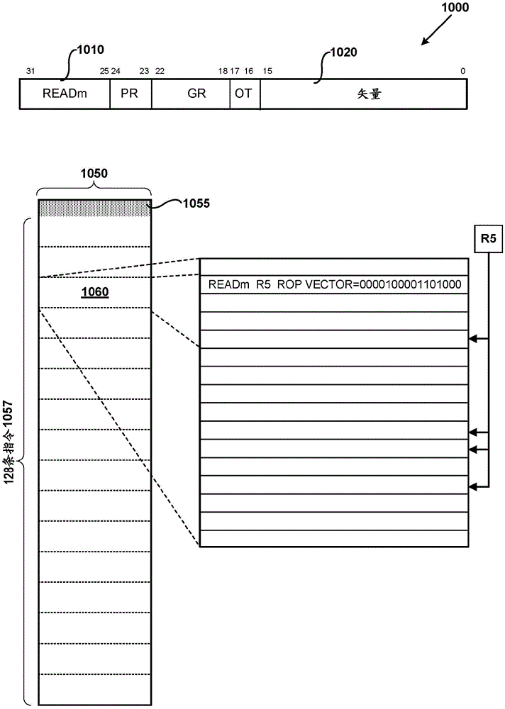
FIG. 10 illustrates an example instruction format 1000 that may send instruction data to multiple target instructions using a vector format. The instruction includes an opcode 1010, which may be the same opcode as a corresponding fixed length instruction, or in other examples a different opcode. The instruction also includes Operand Type (OT) fields at bits 17 and 16 that indicate the type of target operand or operands to which the instruction will issue data. In the illustrated example, the OT field is encoded to indicate the right operand. Other instructions may be encoded with an OT field that indicates a predicate, a left operand, or other suitable target operand type. The instruction also includes a vector field 1020 that includes 16 bits, each bit associated with a target instruction to which target operand data is to be sent. FIG. 10 also illustrates an example instruction block 1050 that includes an instruction header 1055 and 128 instructions 1057 grouped into 16-bit chunks as indicated by the dashed lines. The example instruction is included in the second word of the third 16-bit block 1060. The illustrated instruction is a register read instruction from register number 5, and the OT field is set to ROP. Thus, the value of register 5 will be read from the register file and sent to each instruction indicated by the vector. In the illustrated example, the vector is 0000100001101000. Thus, the value of register 5 will be sent to instruction number 4, instruction number 9, instruction number 10, and instruction number 12. Thus, more than two instructions may target a single instruction using the illustrated instruction format. However, this instruction is limited in that only instructions within the chunks may target variable length target instructions (e.g., only instructions with the third instruction chunk 1060 contain instructions with target operand vectors).
In an alternative example, the vector format instruction is re-encoded so that the 16 bits for the vector may be combined with the bits used in the OT field. In this case, the instruction blocks may be arranged in 6-bit chunks, and up to 6 instructions of each type (predicate, left operand, right operand) may receive data from a single vector instruction. In some examples, the instructions are arranged such that the predicate target instruction is offset by a fixed amount from the vector target instruction, the right operand target instruction is offset by an additional 6 instructions, and the left operand target instruction is offset by an additional 6 instructions, thereby allowing the vector format to send results to a large number of target instructions.
Fig. 11 illustrates an alternative implementation of a target vector instruction as may be implemented in certain examples of the disclosed technology. In the illustrated example, the relative positions of instructions within a 16-bit instruction group block of the instruction block 1110 determine which block of target operands the instruction vector is to send. Thus, the first instruction 1120 is located in the second word of the third set 1130 of instruction blocks 1110. Thus, four instructions associated with an instruction vector will be sent to instructions located within the second set of blocks. Similarly, eighth instruction 1125 is also a target vector instruction, and because it is located at the eighth word, all values produced by the read instruction (here, the read of register 8) will be sent to the various instructions indicated by the vectors within the eighth chunk 1135 of instructions of the instruction block. Thus, instructions may be targeted based at least in part on the location of the instructions within the instruction group blocks of the instruction block.
Example Block-based processor and memory configurations
Fig. 12 is a diagram 1200 illustrating an apparatus including a block-based processor 1210 that includes a control unit 1220 configured to execute instruction blocks including instructions having a variable number of target operands. The control unit 1220 includes a core scheduler. The core scheduler 1225 schedules the flow of instruction blocks, which includes allocation and de-allocation of cores to perform instruction processing, control of input data and output data between any of the cores, register files, memory interfaces, and/or I/O interfaces.
Block-based processor 1210 also includes one or more processor cores 1240-747 configured to retrieve and execute instruction blocks. Each of these cores includes an instruction decoder (e.g., decoder 1249) that decodes the instruction opcode, extended opcode, and other fields to determine whether the instruction specifies a variable number and/or similarity of target operands. The illustrated block-based processor 1210 has up to 8 cores, but in other examples may have 64, 512, 1024, or other numbers of block-based processor cores. Block-based processor 1210 is coupled to memory 1250, memory 1250 including instruction blocks a and B including instructions having a variable number of target operands (1255 and 1256); and is coupled to a computer readable storage medium disk 1260 that stores instructions having a variable number of target operands 1265.
XI exemplary methods of decoding and executing instructions with variable target operands
Fig. 13 is a flowchart 1300 outlining an example method of decoding and executing an instruction having a variable number of target operands as may be performed in certain examples of the disclosed technology. For example, the block-based processor of fig. 1, including block-based processor core 111 described above in fig. 2, may be used to perform the outlined method. In some examples, an instruction decoder of a block-based processor is configured to decode an instruction having a variable number of target operands and execute the decoded instruction, including sending data to a specified target operand and then to a specified target instruction.
At process block 1310, one or more instructions from a block-based processor instruction block are decoded. At least one of the coded instructions specifies two or more targets for sending results of operations associated with the respective instruction. Depending on the particular instruction format employed, the same instruction format may be used to specify one target, two targets, three targets, or more targets.
At process block 1320, the decoded instruction is executed by performing the operation specified by the instruction opcode and by sending the result to the specified target decoded at process block 1310. In some examples, a variable number of target operands may be specified by using a specified opcode, a field specifying the number and/or type of target operands, followed by a number of designators indicating the target instruction. In other examples, the target instructions are encoded with a plurality of target operands using a target vector that includes bits specifying each instruction to send the results of the operations performed by the instructions. In some examples, the target operand target instruction is identified to be sent to based at least in part on a relative position of the decoded instruction within the instruction block. In some examples, the instruction encodes multiple target operands, but the multiple target operands are all for the same type, e.g., predicate, left operand, or right operand. In other examples, the specified target operands may be used in multiple types. In some examples, the instruction having multiple targets is a register read instruction, while in other examples, the processor allows any operation that produces a value to have a variable number of target operands. In some examples, a control unit (e.g., control unit 205) includes a hardware structure that may buffer one or more of the target operands for a consecutive number of clock cycles. In some examples, each instruction includes a buffer that can store its respective left operand, right operand, and predicate operand until the instruction issues and executes. In other examples, a buffer in the hardware structure of the control unit stores the target operands until one or more received target instructions are ready to issue and execute.
Xii example source code and object code
14A-14B illustrate examples of source code 1410 and corresponding assembly code 1420 and 1430 for a block-based processor as may be used in certain examples of the disclosed technology. The source code 1410 includes if/else statements. The statements within each portion of the if/else statement include several memory reads and memory writes to the arrays a [ ] and b [ ]. When source code 1410 is converted to assembly code (and subsequently stored as machine code in object code), a number of load and store assembly instructions will be generated.
Assembly code 1420 for source code portion 1410 includes 28 instructions numbered 0 through 27. Assembly instructions do not include variable target operands and thus no instruction can target more than two target instructions. In some cases, broadcast channels (e.g., B1R and B2P) are used to send values to more than one or two target instructions. Assembly code indicates several fields, such as an instruction opcode, source data specified by the instruction (e.g., a broadcast identifier or immediate parameter), and a target specification. Assembly code includes register read instructions (0 through 3), arithmetic instructions (e.g., instructions 3 and 4), and move instructions that send data to multiple targets (e.g., move instructions 5 and 6). Assembly code 1420 also includes a test instruction 11 that tests whether or not it is greater than the instruction that will generate the predicate value on broadcast channel 2 (B2P). Further, the assembly code includes two non-interruptible memory load instructions 7 and 8 and a predicated memory load instruction 16 and 23. Assembly code 1420 also includes a number of memory store instructions that store data to memory addresses, e.g., predicated store instructions 12, 13, 18, and 26.
In addition to using the broadcast channel, the assembly code also replicates values using MOV instructions. For example, LD instruction 7 performs a memory read from address a [ i ] and sends the value to MOV instruction 8. The value is then copied to instruction 13, the left operand, and instruction 11, the left operand. This additional MOV instruction is used because the 32-bit fixed length instruction format allows only one target operand for the LD instruction.
Turning to FIG. 14B, assembly code section 1430 for source code section 1410 has been re-encoded to use a variable length target operand format. This reduces the total instruction count by 7 instructions and uses only the additional two instruction code words for the extended target portion. The instruction ID is not changed for comparison with assembly code portion 1420, but the instructions may be compressed to take up less space. For example, instruction 2 has been replaced with a READV instruction that encodes two left operand targets ( instruction IDs 15L and 22L) and two right operand targets ( instruction IDs 19R and 24R). The instruction format discussed above with respect to fig. 9 may be used to encode these two different target operand types using a single instruction and an additional instruction data word. In other examples, the READX instruction discussed in FIG. 8 may be used to encode instruction 2. The associated MOV instructions 14 and 21 shown in assembly code section 1420 have also been eliminated.
Instructions 3 and 11 have been encoded using the vector format discussed above with respect to fig. 10. It should be noted that all operands are of the same type, which will be specified in the encoded OT field of the instruction. This may save several instructions, for example, instruction 11 is encoded in a vector format with seven target instructions. The re-encoded assembly code section 1430 also eliminates the use of a broadcast channel. In some examples, a processor core may be optimized by eliminating the use of a broadcast channel and using variable target operand instructions and associated hardware. Further, the use of the broadcast id bit may be assigned to other functions, or to extend the bits used in other instruction fields (e.g., for encoding immediate values).
Assembly code portions 1420 and 1430 may be converted into machine code for actual execution by the block-based processor. For example, depending on the particular machine architecture and compiler parameters, assembly code may be encoded using fixed length instruction formats similar to those discussed above with respect to fig. 5 and variable operand instruction formats discussed above with respect to fig. 7-11. In some examples, some instruction formats may be selected based on performance versus code density targets.
Exemplary method of transcoding XIII
Fig. 15 is a flowchart 1500 outlining an example method of generating computer executable code for a block-based processor as may be performed in certain examples of the disclosed technology. For example, the block-based processor of fig. 1, including block-based processor core 111 described above in fig. 2, may be used to perform the outlined method. In other examples, a general purpose RISC or CISC processor is used to generate instructions to be executed by the block-based processor. In some examples, the code is converted by a compiler and stored as object code that can be executed by a block-based processor. In some examples, a just-in-time compiler or interpreter generates computer executable code at runtime.
At process block 1510, source code and/or object code is analyzed to determine operand dependencies for instruction blocks to be accommodated by a compiler or interpreter. For example, a compiler may analyze to determine that the same target operand is to be sent to multiple different instructions. In some examples, parameters such as code size, execution speed, broadcast channel availability, instruction address space, and other suitable parameters are analyzed in conjunction with the source code to determine operand dependencies. After analyzing the operand dependencies, the method proceeds to process block 1520.
At process block 1520, the source code and/or object code analyzed at process block 1510 is converted into computer-executable code for one or more instruction blocks, the computer-executable code including instructions that encode target operands according to a variable length format. In some examples, an instruction format similar to that discussed above with respect to fig. 7 encodes a variable number of target operands by specifying an instruction identifier for each target operand. In other examples, the variable length target operands are specified using vectors similar to those discussed above with respect to fig. 10 and 11. Once the code has been converted into block-based processor code, it may be stored in a computer-readable storage medium or transmitted over a computer network to another location for execution by the block-based processor.
In some examples of the method, the compiler assigns a priority to target operands that target a single variable length instruction having a variable number of target operands. The compiler may then arrange the order of the target operands such that higher priority target operands are set to their target instructions before lower priority target operands. For example, if certain target instructions have different latency or other execution requirements, their target operands may be ordered accordingly in order to improve execution of the entire instruction block. In some examples, the compiler reorders the extended instructions and/or target instructions such that all target instructions of the instruction for sending multiple target operands will be located within a portion of the instruction block that can be addressed by the descending instruction. In some examples of the method, the method further comprises: a location of an instruction within an instruction block of the translated code is determined that will cause a processor executing the instruction to send a variable number of target operands to the instruction block based at least in part on the location of the send instruction.
Once the code has been converted into block-based processor code, the code may be stored in a computer-readable storage medium or transmitted over a computer network to another location for execution by the block-based processor.
XIV. exemplary computing Environment
FIG. 16 illustrates a general example of a suitable computing environment 1600 in which described embodiments, methods, and techniques, including configuring block-based processors, may be implemented. For example, as described herein, the computing environment 1600 may implement the disclosed techniques for configuring a processor to generate relative ordering data for one or more instruction blocks, or compile code into computer-executable instructions for performing these operations.
The computing environment 1600 is not intended to suggest any limitation as to the scope of use or functionality of the technology, as the technology may be implemented in diverse general-purpose or special-purpose computing environments. For example, the disclosed technology may be implemented with other computer system configurations, including hand-held devices, multiprocessor systems, programmable consumer electronics, network PCs, minicomputers, mainframe computers, and the like. The disclosed technology may also be practiced in distributed computing environments where tasks are performed by remote processing devices that are linked through a communications network. In a distributed computing environment, program modules (including executable instructions for block-based instruction blocks) may be located in both local and remote memory storage devices.
Referring to fig. 16, computing environment 1600 includes at least one block-based processing unit 1610 and memory 1620. In fig. 16, this most basic configuration 1630 is included within the dashed line. Block-based processing unit 1610 executes computer-executable instructions and may be a real processor or a virtual processor. In a multi-processing system, multiple processing units execute computer-executable instructions to increase processing power, so that multiple processors may run concurrently. The memory 1620 may be volatile memory (e.g., registers, cache, RAM), non-volatile memory (e.g., ROM, EEPROM, flash memory, etc.), or some combination of the two. Memory 1620 stores software 1680, images, and video, which may implement techniques described herein, for example. The computing environment may have additional features. For example, computing environment 1600 includes memory 1640, one or more input devices 1650, one or more output devices 1660, and one or more communication connections 1670. An interconnection mechanism (not shown) such as a bus, controller, or network interconnects the components of the computing environment 1600. Typically, operating system software (not shown) provides an operating environment for other software executing in the computing environment 1600, and coordinates activities of the components of the computing environment 1600.
The memory 1640 may be removable or non-removable and include magnetic disks, magnetic tapes or cassettes, CD-ROMs, CD-RWs, DVDs, or any other medium which can be used to store information and which can be accessed within the computing environment 1600. Storage 1640 stores instructions, plug-in data, and messages for software 1680, which may be used to implement the techniques described herein.
The one or more input devices 1650 can be a touch input device such as a keyboard, keypad, mouse, touch screen display, pen, or trackball; a voice input device; a scanning device; or another device that provides input to the computing environment 1600. For audio, the one or more input devices 1650 can be a sound card or similar device that accepts audio input in analog or digital form, or a CD-ROM reader that provides audio samples to the computing environment 1600. One or more output devices 1660 can be a display, printer, speaker, CD writer, or another device that provides output from the computing environment 1600.
One or more communication connections 1670 enable communication over a communication medium (e.g., a connecting network) to another computing entity. The communication medium conveys information such as computer-executable instructions, compressed graphics information, video, or other data in a modulated data signal. The one or more communication connections 1670 are not limited to wired connections (e.g., megabit or gigabit ethernet, wireless broadband, electrical connections, or fiber channel over fiber optic connections), but also includes wireless technologies (e.g., RF connections via bluetooth, WiFi (IEEE 802.11a/b/n), WiMax, cellular, satellite, laser, infrared) and other suitable communication connections for providing network connectivity for the disclosed methods. In a virtual host environment, one or more communication connections may be virtualized network connections provided by a virtual host.
Some embodiments of the disclosed method may be performed using computer-executable instructions that implement all or a portion of the disclosed techniques in the computing cloud 1690. For example, the disclosed compiler and/or block-based processor server are located in a computing environment, or the disclosed compiler may execute on a server located in the computing cloud 1690. In some examples, the disclosed compiler executes on a conventional central processing unit (e.g., a RISC or CISC processor).
Computer readable media are any available media that can be accessed within the computing environment 1600. By way of example, and not limitation, with computing environment 1600, computer-readable media include memory 1620 and/or storage 1640. It should be readily understood that the term computer-readable storage medium includes data storage media for data such as memory 1620 and storage 1640, and not transmission media such as modulated data signals.
XV. additional examples of the disclosed technology
In light of the examples discussed above, additional examples of the disclosed subject matter are discussed herein. Additional examples may be further understood by one of ordinary skill in the relevant art with reference to appendix A below.
In some examples of the disclosed technology, an apparatus includes a memory and one or more block-based processor cores. One or more of the processor cores includes an instruction decoder configured to decode target operands of instructions in the instruction block, the instructions encoded to take into account a variable number of target operands; and a control unit configured to send data for each of the decoded target operands of the operation specified by the target instruction.
In some examples, the processor core includes an execution unit configured to perform an operation using at least one of the decoded operands. In some examples, the instruction is encoded with a variable number of instruction targets indicating instruction identifiers for target operands. In some examples, the instruction target also indicates a type of each of the target operands. In other examples, the instruction is encoded with a bit vector indicating the instruction target. In some examples, the one or more types of target operands may be one or more of: an identifier of another instruction within the instruction block, a global register, a broadcast channel, an identifier of another instruction block, and a memory address. In some examples, the field encoding the target operand supports one, multiple, or all types. In some examples, different instruction opcodes are used for different operand types. In some examples, at least one of the target operands indicates a predicate operand, a right operand, or a left operand of an operation performed by the target instruction.
In some examples, the instruction decoder is configured to determine a target instruction to receive target operand data based at least in part on a relative position of the instruction within the instruction block. In some examples, the instruction decoder is configured to decode the target operand based on an extended opcode encoded in a different word of the instruction block. In some examples, the instruction decoder is configured to decode the instruction into a fixed length instruction or a variable number of target instructions based at least in part on an opcode of the instruction encoded in the instruction block.
In some examples of the disclosed technology, a method of operating a processor to execute instruction blocks includes: decoding one or more instructions from an instruction block, at least one of the decoded instructions specifying two or more targets for sending results of operations associated with the respective instruction; executing the decoded instruction by performing an operation; and sending the results to the specified two or more targets.
In some examples, the transcoding includes: the specified two or more targets are determined based at least in part on a relative position of the coded instruction within the instruction block or a relative position of the coded instruction within a portion of the instruction block. In some examples, two relative positions of the decoded instructions are used.
In some examples, the transcoding includes: the specified two or more targets are determined based at least in part on the vector. In some examples, the transcoding includes: decoding data indicative of a number of target operands having a particular type, and determining a target location to send the data for the particular type of target operand.
In some examples, the transcoding includes: the type of the target instruction operand is determined. Examples of suitable operand types include a left operand, a right operand, and an assert operand. In some examples, the target operand type may be specified in different ways (e.g., as numbers or letters) or include different types (e.g., different types for integer and fixed-point values). In some examples, complex predicate operands are specified, or no predicate operands are specified. In some examples, the transcoding includes: the type of the target instruction operand is determined, and the type may be any one or more of: target instructions, broadcast channels, registers, and memory. In some examples, the broadcast channel is not of a supported type. In some examples, the register is not of the supported type. In some examples, the memory is not of a supported type. In some examples, the target instruction is not of a supported type. In some examples, the target instruction is a type that is only supported, or a type that is only supported for certain opcode classes.
In some examples, the instruction is a register read. In some examples, the additional instructions may support a variable number of target instructions, e.g., arithmetic instructions, logical instructions, and/or move instructions.
In some examples of the disclosed technology, a method of compiling source object code and/or link object code for a block-based processor comprises: the source code and/or object code is analyzed to determine operand dependencies for the instruction block, and the source code and/or object code is converted into computer-executable code for the instruction block, the computer-executable code including instructions that encode target operands according to a variable length format. In some examples, the method is performed by executing computer readable instructions on a block-based processor. In other examples, the method is performed by executing computer readable instructions on a general-purpose processor or a special-purpose processor (e.g., a CISC or RISC CPU; or a GPU or other special-purpose co-processor).
In some examples, a compilation method includes: the target operands are assigned priorities and are arranged such that higher priority target operands will be sent to their target instructions before lower priority target operands. In some examples, the method comprises: the target instructions are reordered such that all target instructions for an instruction that issues multiple target operands will all be located within a portion of the instruction block that can be addressed by the issue instruction.
In some examples, the method comprises: a location of an instruction within an instruction block of the translated code is determined that will cause a processor executing the instruction to send a variable target operand to a chunk of the instruction based at least in part on the location.
In some examples, a computer-readable storage medium stores computer-readable instructions for a block of instructions that, when executed by a processor, cause the processor to perform any one or more of the disclosed methods.
In view of the many possible embodiments to which the principles of the disclosed subject matter may be applied, it should be recognized that the illustrated embodiments are only preferred examples and should not be taken as limiting the scope of the claims to those preferred examples. Rather, the scope of the claimed subject matter is defined by the following claims. We therefore claim as our invention all that comes within the scope of these claims.