CN108200367B - Pixel unit, method for forming pixel unit and digital camera imaging system assembly - Google Patents
Pixel unit, method for forming pixel unit and digital camera imaging system assembly Download PDFInfo
- Publication number
- CN108200367B CN108200367B CN201810099793.5A CN201810099793A CN108200367B CN 108200367 B CN108200367 B CN 108200367B CN 201810099793 A CN201810099793 A CN 201810099793A CN 108200367 B CN108200367 B CN 108200367B
- Authority
- CN
- China
- Prior art keywords
- transistor
- global exposure
- exposure
- capacitor
- substrate
- Prior art date
- Legal status (The legal status is an assumption and is not a legal conclusion. Google has not performed a legal analysis and makes no representation as to the accuracy of the status listed.)
- Active
Links
- 238000003384 imaging method Methods 0.000 title claims description 19
- 238000000034 method Methods 0.000 title claims description 17
- 239000003990 capacitor Substances 0.000 claims abstract description 96
- 239000000758 substrate Substances 0.000 claims abstract description 69
- 238000005096 rolling process Methods 0.000 claims abstract description 53
- 239000004065 semiconductor Substances 0.000 claims abstract description 31
- 238000012546 transfer Methods 0.000 claims abstract description 26
- 238000005070 sampling Methods 0.000 claims abstract description 20
- 230000002596 correlated effect Effects 0.000 claims abstract description 13
- 230000004044 response Effects 0.000 claims abstract description 7
- 238000007667 floating Methods 0.000 claims description 38
- 230000003321 amplification Effects 0.000 claims description 9
- 230000000875 corresponding effect Effects 0.000 claims description 9
- 238000003199 nucleic acid amplification method Methods 0.000 claims description 9
- 239000013078 crystal Substances 0.000 claims description 5
- 238000005286 illumination Methods 0.000 claims description 5
- 230000003071 parasitic effect Effects 0.000 claims description 3
- 230000003287 optical effect Effects 0.000 claims description 2
- 238000010586 diagram Methods 0.000 description 17
- 238000009792 diffusion process Methods 0.000 description 14
- 235000012431 wafers Nutrition 0.000 description 13
- 238000006243 chemical reaction Methods 0.000 description 12
- 239000002184 metal Substances 0.000 description 11
- 238000004519 manufacturing process Methods 0.000 description 6
- 238000005516 engineering process Methods 0.000 description 5
- 239000000463 material Substances 0.000 description 5
- 230000008569 process Effects 0.000 description 5
- 230000008901 benefit Effects 0.000 description 4
- 230000002093 peripheral effect Effects 0.000 description 4
- 108010076504 Protein Sorting Signals Proteins 0.000 description 3
- 238000009825 accumulation Methods 0.000 description 3
- 230000009286 beneficial effect Effects 0.000 description 3
- 230000002708 enhancing effect Effects 0.000 description 3
- 239000012212 insulator Substances 0.000 description 3
- 238000012545 processing Methods 0.000 description 3
- 230000005540 biological transmission Effects 0.000 description 2
- 230000000295 complement effect Effects 0.000 description 2
- 230000001276 controlling effect Effects 0.000 description 2
- 230000007423 decrease Effects 0.000 description 2
- 238000013461 design Methods 0.000 description 2
- 230000000694 effects Effects 0.000 description 2
- 230000005669 field effect Effects 0.000 description 2
- 230000010354 integration Effects 0.000 description 2
- 230000004048 modification Effects 0.000 description 2
- 238000012986 modification Methods 0.000 description 2
- 230000009467 reduction Effects 0.000 description 2
- 238000003860 storage Methods 0.000 description 2
- 230000002123 temporal effect Effects 0.000 description 2
- 238000007514 turning Methods 0.000 description 2
- 101100248200 Arabidopsis thaliana RGGB gene Proteins 0.000 description 1
- 206010034960 Photophobia Diseases 0.000 description 1
- 241000593989 Scardinius erythrophthalmus Species 0.000 description 1
- XUIMIQQOPSSXEZ-UHFFFAOYSA-N Silicon Chemical compound [Si] XUIMIQQOPSSXEZ-UHFFFAOYSA-N 0.000 description 1
- 238000010521 absorption reaction Methods 0.000 description 1
- 230000015572 biosynthetic process Effects 0.000 description 1
- 239000003086 colorant Substances 0.000 description 1
- 230000008878 coupling Effects 0.000 description 1
- 238000010168 coupling process Methods 0.000 description 1
- 238000005859 coupling reaction Methods 0.000 description 1
- 230000000779 depleting effect Effects 0.000 description 1
- 230000008014 freezing Effects 0.000 description 1
- 238000007710 freezing Methods 0.000 description 1
- 230000006870 function Effects 0.000 description 1
- 230000031700 light absorption Effects 0.000 description 1
- 208000013469 light sensitivity Diseases 0.000 description 1
- 238000003754 machining Methods 0.000 description 1
- 239000011159 matrix material Substances 0.000 description 1
- 229910044991 metal oxide Inorganic materials 0.000 description 1
- 150000004706 metal oxides Chemical class 0.000 description 1
- 229910052710 silicon Inorganic materials 0.000 description 1
- 239000010703 silicon Substances 0.000 description 1
- 238000005549 size reduction Methods 0.000 description 1
- 238000003786 synthesis reaction Methods 0.000 description 1
Images




Classifications
-
- H—ELECTRICITY
- H04—ELECTRIC COMMUNICATION TECHNIQUE
- H04N—PICTORIAL COMMUNICATION, e.g. TELEVISION
- H04N25/00—Circuitry of solid-state image sensors [SSIS]; Control thereof
- H04N25/70—SSIS architectures; Circuits associated therewith
- H04N25/76—Addressed sensors, e.g. MOS or CMOS sensors
-
- H—ELECTRICITY
- H04—ELECTRIC COMMUNICATION TECHNIQUE
- H04N—PICTORIAL COMMUNICATION, e.g. TELEVISION
- H04N25/00—Circuitry of solid-state image sensors [SSIS]; Control thereof
- H04N25/60—Noise processing, e.g. detecting, correcting, reducing or removing noise
- H04N25/616—Noise processing, e.g. detecting, correcting, reducing or removing noise involving a correlated sampling function, e.g. correlated double sampling [CDS] or triple sampling
-
- H—ELECTRICITY
- H04—ELECTRIC COMMUNICATION TECHNIQUE
- H04N—PICTORIAL COMMUNICATION, e.g. TELEVISION
- H04N23/00—Cameras or camera modules comprising electronic image sensors; Control thereof
- H04N23/10—Cameras or camera modules comprising electronic image sensors; Control thereof for generating image signals from different wavelengths
- H04N23/11—Cameras or camera modules comprising electronic image sensors; Control thereof for generating image signals from different wavelengths for generating image signals from visible and infrared light wavelengths
-
- H—ELECTRICITY
- H04—ELECTRIC COMMUNICATION TECHNIQUE
- H04N—PICTORIAL COMMUNICATION, e.g. TELEVISION
- H04N23/00—Cameras or camera modules comprising electronic image sensors; Control thereof
- H04N23/50—Constructional details
- H04N23/54—Mounting of pick-up tubes, electronic image sensors, deviation or focusing coils
-
- H—ELECTRICITY
- H04—ELECTRIC COMMUNICATION TECHNIQUE
- H04N—PICTORIAL COMMUNICATION, e.g. TELEVISION
- H04N23/00—Cameras or camera modules comprising electronic image sensors; Control thereof
- H04N23/70—Circuitry for compensating brightness variation in the scene
-
- H—ELECTRICITY
- H04—ELECTRIC COMMUNICATION TECHNIQUE
- H04N—PICTORIAL COMMUNICATION, e.g. TELEVISION
- H04N25/00—Circuitry of solid-state image sensors [SSIS]; Control thereof
- H04N25/50—Control of the SSIS exposure
- H04N25/53—Control of the integration time
- H04N25/531—Control of the integration time by controlling rolling shutters in CMOS SSIS
-
- H—ELECTRICITY
- H04—ELECTRIC COMMUNICATION TECHNIQUE
- H04N—PICTORIAL COMMUNICATION, e.g. TELEVISION
- H04N25/00—Circuitry of solid-state image sensors [SSIS]; Control thereof
- H04N25/50—Control of the SSIS exposure
- H04N25/53—Control of the integration time
- H04N25/532—Control of the integration time by controlling global shutters in CMOS SSIS
-
- H—ELECTRICITY
- H04—ELECTRIC COMMUNICATION TECHNIQUE
- H04N—PICTORIAL COMMUNICATION, e.g. TELEVISION
- H04N25/00—Circuitry of solid-state image sensors [SSIS]; Control thereof
- H04N25/50—Control of the SSIS exposure
- H04N25/57—Control of the dynamic range
- H04N25/59—Control of the dynamic range by controlling the amount of charge storable in the pixel, e.g. modification of the charge conversion ratio of the floating node capacitance
-
- H—ELECTRICITY
- H04—ELECTRIC COMMUNICATION TECHNIQUE
- H04N—PICTORIAL COMMUNICATION, e.g. TELEVISION
- H04N25/00—Circuitry of solid-state image sensors [SSIS]; Control thereof
- H04N25/60—Noise processing, e.g. detecting, correcting, reducing or removing noise
- H04N25/67—Noise processing, e.g. detecting, correcting, reducing or removing noise applied to fixed-pattern noise, e.g. non-uniformity of response
- H04N25/671—Noise processing, e.g. detecting, correcting, reducing or removing noise applied to fixed-pattern noise, e.g. non-uniformity of response for non-uniformity detection or correction
-
- H—ELECTRICITY
- H04—ELECTRIC COMMUNICATION TECHNIQUE
- H04N—PICTORIAL COMMUNICATION, e.g. TELEVISION
- H04N25/00—Circuitry of solid-state image sensors [SSIS]; Control thereof
- H04N25/70—SSIS architectures; Circuits associated therewith
- H04N25/76—Addressed sensors, e.g. MOS or CMOS sensors
- H04N25/77—Pixel circuitry, e.g. memories, A/D converters, pixel amplifiers, shared circuits or shared components
-
- H—ELECTRICITY
- H04—ELECTRIC COMMUNICATION TECHNIQUE
- H04N—PICTORIAL COMMUNICATION, e.g. TELEVISION
- H04N25/00—Circuitry of solid-state image sensors [SSIS]; Control thereof
- H04N25/70—SSIS architectures; Circuits associated therewith
- H04N25/76—Addressed sensors, e.g. MOS or CMOS sensors
- H04N25/77—Pixel circuitry, e.g. memories, A/D converters, pixel amplifiers, shared circuits or shared components
- H04N25/771—Pixel circuitry, e.g. memories, A/D converters, pixel amplifiers, shared circuits or shared components comprising storage means other than floating diffusion
-
- H—ELECTRICITY
- H04—ELECTRIC COMMUNICATION TECHNIQUE
- H04N—PICTORIAL COMMUNICATION, e.g. TELEVISION
- H04N25/00—Circuitry of solid-state image sensors [SSIS]; Control thereof
- H04N25/70—SSIS architectures; Circuits associated therewith
- H04N25/76—Addressed sensors, e.g. MOS or CMOS sensors
- H04N25/78—Readout circuits for addressed sensors, e.g. output amplifiers or A/D converters
-
- H—ELECTRICITY
- H04—ELECTRIC COMMUNICATION TECHNIQUE
- H04N—PICTORIAL COMMUNICATION, e.g. TELEVISION
- H04N25/00—Circuitry of solid-state image sensors [SSIS]; Control thereof
- H04N25/70—SSIS architectures; Circuits associated therewith
- H04N25/79—Arrangements of circuitry being divided between different or multiple substrates, chips or circuit boards, e.g. stacked image sensors
-
- H—ELECTRICITY
- H10—SEMICONDUCTOR DEVICES; ELECTRIC SOLID-STATE DEVICES NOT OTHERWISE PROVIDED FOR
- H10F—INORGANIC SEMICONDUCTOR DEVICES SENSITIVE TO INFRARED RADIATION, LIGHT, ELECTROMAGNETIC RADIATION OF SHORTER WAVELENGTH OR CORPUSCULAR RADIATION
- H10F39/00—Integrated devices, or assemblies of multiple devices, comprising at least one element covered by group H10F30/00, e.g. radiation detectors comprising photodiode arrays
- H10F39/011—Manufacture or treatment of image sensors covered by group H10F39/12
- H10F39/018—Manufacture or treatment of image sensors covered by group H10F39/12 of hybrid image sensors
-
- H—ELECTRICITY
- H10—SEMICONDUCTOR DEVICES; ELECTRIC SOLID-STATE DEVICES NOT OTHERWISE PROVIDED FOR
- H10F—INORGANIC SEMICONDUCTOR DEVICES SENSITIVE TO INFRARED RADIATION, LIGHT, ELECTROMAGNETIC RADIATION OF SHORTER WAVELENGTH OR CORPUSCULAR RADIATION
- H10F39/00—Integrated devices, or assemblies of multiple devices, comprising at least one element covered by group H10F30/00, e.g. radiation detectors comprising photodiode arrays
- H10F39/10—Integrated devices
- H10F39/12—Image sensors
- H10F39/18—Complementary metal-oxide-semiconductor [CMOS] image sensors; Photodiode array image sensors
- H10F39/182—Colour image sensors
-
- H—ELECTRICITY
- H10—SEMICONDUCTOR DEVICES; ELECTRIC SOLID-STATE DEVICES NOT OTHERWISE PROVIDED FOR
- H10F—INORGANIC SEMICONDUCTOR DEVICES SENSITIVE TO INFRARED RADIATION, LIGHT, ELECTROMAGNETIC RADIATION OF SHORTER WAVELENGTH OR CORPUSCULAR RADIATION
- H10F39/00—Integrated devices, or assemblies of multiple devices, comprising at least one element covered by group H10F30/00, e.g. radiation detectors comprising photodiode arrays
- H10F39/80—Constructional details of image sensors
- H10F39/802—Geometry or disposition of elements in pixels, e.g. address-lines or gate electrodes
- H10F39/8023—Disposition of the elements in pixels, e.g. smaller elements in the centre of the imager compared to larger elements at the periphery
-
- H—ELECTRICITY
- H10—SEMICONDUCTOR DEVICES; ELECTRIC SOLID-STATE DEVICES NOT OTHERWISE PROVIDED FOR
- H10F—INORGANIC SEMICONDUCTOR DEVICES SENSITIVE TO INFRARED RADIATION, LIGHT, ELECTROMAGNETIC RADIATION OF SHORTER WAVELENGTH OR CORPUSCULAR RADIATION
- H10F39/00—Integrated devices, or assemblies of multiple devices, comprising at least one element covered by group H10F30/00, e.g. radiation detectors comprising photodiode arrays
- H10F39/80—Constructional details of image sensors
- H10F39/803—Pixels having integrated switching, control, storage or amplification elements
-
- H—ELECTRICITY
- H10—SEMICONDUCTOR DEVICES; ELECTRIC SOLID-STATE DEVICES NOT OTHERWISE PROVIDED FOR
- H10F—INORGANIC SEMICONDUCTOR DEVICES SENSITIVE TO INFRARED RADIATION, LIGHT, ELECTROMAGNETIC RADIATION OF SHORTER WAVELENGTH OR CORPUSCULAR RADIATION
- H10F39/00—Integrated devices, or assemblies of multiple devices, comprising at least one element covered by group H10F30/00, e.g. radiation detectors comprising photodiode arrays
- H10F39/80—Constructional details of image sensors
- H10F39/805—Coatings
- H10F39/8053—Colour filters
-
- H—ELECTRICITY
- H10—SEMICONDUCTOR DEVICES; ELECTRIC SOLID-STATE DEVICES NOT OTHERWISE PROVIDED FOR
- H10F—INORGANIC SEMICONDUCTOR DEVICES SENSITIVE TO INFRARED RADIATION, LIGHT, ELECTROMAGNETIC RADIATION OF SHORTER WAVELENGTH OR CORPUSCULAR RADIATION
- H10F39/00—Integrated devices, or assemblies of multiple devices, comprising at least one element covered by group H10F30/00, e.g. radiation detectors comprising photodiode arrays
- H10F39/80—Constructional details of image sensors
- H10F39/809—Constructional details of image sensors of hybrid image sensors
-
- H—ELECTRICITY
- H10—SEMICONDUCTOR DEVICES; ELECTRIC SOLID-STATE DEVICES NOT OTHERWISE PROVIDED FOR
- H10F—INORGANIC SEMICONDUCTOR DEVICES SENSITIVE TO INFRARED RADIATION, LIGHT, ELECTROMAGNETIC RADIATION OF SHORTER WAVELENGTH OR CORPUSCULAR RADIATION
- H10F39/00—Integrated devices, or assemblies of multiple devices, comprising at least one element covered by group H10F30/00, e.g. radiation detectors comprising photodiode arrays
- H10F39/80—Constructional details of image sensors
- H10F39/811—Interconnections
-
- H—ELECTRICITY
- H10—SEMICONDUCTOR DEVICES; ELECTRIC SOLID-STATE DEVICES NOT OTHERWISE PROVIDED FOR
- H10F—INORGANIC SEMICONDUCTOR DEVICES SENSITIVE TO INFRARED RADIATION, LIGHT, ELECTROMAGNETIC RADIATION OF SHORTER WAVELENGTH OR CORPUSCULAR RADIATION
- H10F39/00—Integrated devices, or assemblies of multiple devices, comprising at least one element covered by group H10F30/00, e.g. radiation detectors comprising photodiode arrays
- H10F39/80—Constructional details of image sensors
- H10F39/813—Electronic components shared by multiple pixels, e.g. one amplifier shared by two pixels
-
- H—ELECTRICITY
- H04—ELECTRIC COMMUNICATION TECHNIQUE
- H04N—PICTORIAL COMMUNICATION, e.g. TELEVISION
- H04N2209/00—Details of colour television systems
- H04N2209/04—Picture signal generators
- H04N2209/041—Picture signal generators using solid-state devices
- H04N2209/042—Picture signal generators using solid-state devices having a single pick-up sensor
- H04N2209/045—Picture signal generators using solid-state devices having a single pick-up sensor using mosaic colour filter
Landscapes
- Engineering & Computer Science (AREA)
- Multimedia (AREA)
- Signal Processing (AREA)
- Solid State Image Pick-Up Elements (AREA)
- Transforming Light Signals Into Electric Signals (AREA)
Abstract
一种像素单元,包括光电二极管,传输晶体管,复位晶体管,动态范围增强电容,电容控制晶体管,放大晶体管,滚动曝光行选择晶体管及读出电路块。所述光电二极管,传输晶体管,复位晶体管,动态范围增强电容,电容控制晶体管,源极跟随放大晶体管和滚动曝光行选择晶体管设置在第一半导体芯片的第一基底内,用于累积图像电荷以响应入射到光电二极管上的光。所述读出电路块可部分地设置在第二半导体芯片的第二基底内,部分地设置在第一基底内,其中所述读出电路块根据应用程序设定包含可选的滚动曝光模式和全局曝光模式。全局曝光模式提供像素内相关双采样。
A pixel unit includes a photodiode, a transfer transistor, a reset transistor, a dynamic range enhancement capacitor, a capacitor control transistor, an amplifying transistor, a rolling exposure row selection transistor and a readout circuit block. The photodiode, transfer transistor, reset transistor, dynamic range enhancement capacitor, capacitor control transistor, source follower amplifying transistor and rolling exposure line selection transistor are provided in the first substrate of the first semiconductor chip for accumulating image charges in response to Light incident on a photodiode. The readout circuit block may be disposed partially within the second substrate of the second semiconductor chip and partially within the first substrate, wherein the readout circuit block includes selectable rolling exposure modes and Global exposure mode. Global exposure mode provides intra-pixel correlated double sampling.
Description
技术领域technical field
本发明涉及一种图像传感器,尤其涉及一种堆叠芯片结构的图像传感器像素单元。底部芯片包括用以捕获图像的光感区域和结构阵列。顶部芯片包括电路元件用以从阵列中获取图像。图像传感器可用于数字相机。The present invention relates to an image sensor, in particular to an image sensor pixel unit with a stacked chip structure. The bottom chip includes an array of photosensitive areas and structures to capture images. The top chip includes circuit elements to acquire images from the array. Image sensors can be used in digital cameras.
背景技术Background technique
图像捕获装置一般包括图像传感器和镜头。镜头聚光到图像传感器以形成图像,图像传感器转换光信号到电信号。电信号从图像捕获装置输出到电子系统的其他组件。图像捕获装置和电子系统的其他组件构成图像系统。图像传感器逐渐应用普遍,在各种电子系统中都可见,例如手机,数码相机,医疗设备,以及计算机等。Image capture devices generally include an image sensor and a lens. The lens focuses light onto an image sensor to form an image, and the image sensor converts the light signal to an electrical signal. Electrical signals are output from the image capture device to other components of the electronic system. The image capture device and other components of the electronic system make up the image system. Image sensors are becoming more and more common and can be found in various electronic systems, such as mobile phones, digital cameras, medical equipment, and computers.
一个典型的图像传感器包括一系列光传感图像器件(像素)排列置于两维阵列中。此图像传感器可认为是通过在像素上形成色彩滤镜矩阵(CFA)以产生图像。这种技术过去用于制造图像传感器,尤其是CMOS图像传感器,其技术不断持续向前发展。例如,更高的分辨率和低功耗的需求进一步促进了这些图像传感器的小型化和集成化。然而,小型化会伴随像素光感灵敏度和动态范围的降低,这需要新的方案来解决问题。A typical image sensor consists of a series of light-sensing image devices (pixels) arranged in a two-dimensional array. This image sensor can be thought of as producing an image by forming a color filter matrix (CFA) on the pixels. This technology has been used to manufacture image sensors, especially CMOS image sensors, and its technology has continued to advance. For example, the need for higher resolution and lower power consumption further promotes the miniaturization and integration of these image sensors. However, miniaturization is accompanied by a reduction in pixel light sensitivity and dynamic range, which requires new solutions to solve the problem.
随着像素尺寸的降低,基底内总的光吸收程度对某些光来说变得不充足,尤其是波长较长的光。这成为使用光入射到传感器基底的背面的背照(BSI)技术的图像传感器的典型问题。在BSI技术中,传感器硅基底可以是2微米厚,这足够吸收蓝光但不足以吸收红光,红光充分吸收需要大约10微米厚。As pixel size decreases, the overall level of light absorption within the substrate becomes insufficient for some light, especially longer wavelength light. This becomes a typical problem for image sensors using backside illumination (BSI) technology where light is incident on the backside of the sensor substrate. In BSI technology, the sensor silicon substrate can be 2 microns thick, which is enough to absorb blue light but not red light, which needs to be about 10 microns thick for sufficient red absorption.
将已有的图像传感器形成所称的堆叠传感器是众所周知的技术。这种形式中一种典型的设置方式是,像素阵列中的光电二极管或其他光传感元件形成在第一半导体晶片或层,处理光传感元件的信号的相关电路形成在位于第一半导体晶片或层之上的第二半导体晶片或层。第一和第二半导体晶片或层在这里一般分别指传感器芯片和电路芯片。更准确地说,第一和第二半导体晶片沿着许多其他类似的晶片形成于堆叠的第一和第二半导体晶片上,排列整齐相关的晶片内连后,切割成一般称作为半导体芯片的堆叠器件。堆叠的两个芯片可理解为通常惯例的两个晶片堆叠并且被切割成依旧保留堆叠以形成例如一个堆叠图像传感器的电路系统的芯片。当晶片的互连和芯片内的互连涉及分别形成于留在晶片和芯片上的装置时,晶片的互连连接传感器和电路晶片可被看作芯片内的互连。关于这种设置的好处包括最终的图像传感系统与未堆叠设置的情形相比,占用更少的面积。另外一个好处是,不同的生产方法和材料可用于加工单独优化使用的芯片。Forming existing image sensors into so-called stacked sensors is a well-known technique. A typical arrangement in this format is that the photodiodes or other light-sensing elements in the pixel array are formed on a first semiconductor wafer or layer, and the associated circuitry that processes the signals of the light-sensing elements is formed on the first semiconductor wafer. or layer on top of a second semiconductor wafer or layer. The first and second semiconductor wafers or layers are generally referred to herein as sensor chips and circuit chips, respectively. More precisely, first and second semiconductor wafers are formed on a stack of first and second semiconductor wafers along a number of other similar wafers, aligned with the associated wafers interconnected, and then diced into stacks commonly referred to as semiconductor chips. device. Stacked two chips may be understood as the usual convention of two wafers stacked and diced into chips that still remain stacked to form circuitry such as a stacked image sensor. Wafer interconnects connecting sensors and circuit wafers may be viewed as intra-chip interconnects when they relate to devices formed on the wafer and on the chip, respectively. Benefits regarding this arrangement include that the resulting image sensing system occupies less area than would be the case with an unstacked arrangement. An added benefit is that different production methods and materials can be used to process chips that are individually optimized for use.
两种最普通的读出传感器芯片产生的图像信号的方式是滚动曝光模式和全局曝光模式。滚动曝光模式包括在不同的时间内曝光传感器阵列的不同行并且按选定的顺序读出这些行。全局曝光模式包括同时曝光每一像素并且和操作传统的机械快门相机相同的时间长度。现有的数字图像系统已经实现了滚动曝光或全局曝光的读出模式。成像系统具有两种可选的读出模式是非常有益的。The two most common ways of reading out the image signal produced by the sensor chip are rolling exposure mode and global exposure mode. The rolling exposure mode involves exposing different rows of the sensor array at different times and reading out the rows in a selected order. The global exposure mode involves exposing each pixel simultaneously and for the same length of time as operating a conventional mechanical shutter camera. Existing digital imaging systems have implemented readout modes of rolling exposure or global exposure. It is very beneficial for the imaging system to have two selectable readout modes.
滚动曝光(RS)模式在不同的时间内曝光和读出阵列的相邻行,每行开始和结束其曝光与相邻行有略微的偏移时间。曝光完成后一行接一行地读出且从每行传输电荷到像素的读出节点。虽然每行属于相同的曝光时间,传感器上部的行的曝光时间要早于下部的行的曝光时间。时间有赖于行的数目以及相邻行之间的偏移时间。滚动曝光读出模式一个潜在的问题是空间变形。当一个大的物体以高于读出速率的速率运动时,就容易出现空间变形。另一个问题是曝光图像的不同区域不能及时地精确纠正并在图像中呈现出变形。为提高最后读出的图像信号的信噪比,一般是降低随机噪声,称为相关双采样(CDS)的参考读出在每个像素被放大晶体管放大输出信号变换之前进行操作。放大晶体管可为一源极跟随晶体管或一普通的漏极结构,其中像素采用电压模式读出。然而,包含一个像素采用电流模式输出的普通源放大器是有益的。普通的源放大器可用于大面积的成像器。光电二极管的电流被放大且读出电路通过电容整合电流到电压,然后转换到数字电路区域。Rolling exposure (RS) mode exposes and reads out adjacent rows of the array at different times, with each row beginning and ending its exposure with a slight offset time from the adjacent row. After exposure is complete, readout row by row and transfer charge from each row to the readout node of the pixel. Although each row belongs to the same exposure time, the upper row of the sensor is exposed earlier than the lower row. The time depends on the number of rows and the offset time between adjacent rows. A potential problem with the rolling exposure readout mode is spatial distortion. Spatial deformation is prone to occur when a large object is moving at a rate higher than the readout rate. Another problem is that different areas of the exposed image cannot be accurately corrected in time and appear distorted in the image. To improve the signal-to-noise ratio of the final read-out image signal, generally to reduce random noise, a reference readout called correlated double sampling (CDS) operates before each pixel is transformed by the amplifying transistor amplifying the output signal. The amplifying transistor can be a source follower transistor or a common drain structure, where the pixel uses voltage mode readout. However, it would be beneficial to include a common source amplifier with a current-mode output for one pixel. Common source amplifiers can be used for large area imagers. The current of the photodiode is amplified and the readout circuit integrates the current into a voltage through the capacitor, which is then converted to the digital circuit area.
全局曝光(GS)模式同时曝光阵列中的所有像素。这有利于抓取快速运动的目标,及时冻结。曝光开始前通过耗尽所有的电荷所有像素都复位(RST)到相同的表面暗电平。在曝光开始时每一像素同时收集电荷并在整个曝光期间都允许这样处理。在曝光结束时每一像素同时传输电荷到它的读出点。全局曝光模式可看作是当前面的曝光从每一像素的读出存储点读出时曝光行进的连续操作方式。在这种模式中,传感器具有百分百的占空比来优化时间分辨率和光子收集效率。在滚动曝光模式中的短暂读出阶段的图像中没有这种做法。传感器的不同区域之间准确的时间相关性是必需的这是全局曝光最基本的要求。全局曝光模式也非常容易实现与光源或其他设备同步。Global exposure (GS) mode exposes all pixels in the array simultaneously. This is good for grabbing fast moving targets and freezing in time. All pixels are reset (RST) to the same surface dark level by depleting all charges before exposure begins. Each pixel collects charge simultaneously at the start of exposure and is allowed to do so throughout the exposure period. Each pixel simultaneously transfers charge to its readout point at the end of exposure. The global exposure mode can be viewed as a continuous mode of operation in which exposures progress as the previous exposures are read out from each pixel's readout storage point. In this mode, the sensor has a 100 percent duty cycle to optimize temporal resolution and photon collection efficiency. This is not done in images with brief readout phases in rolling exposure mode. Accurate temporal correlation between different areas of the sensor is required which is the most basic requirement for global exposure. Global exposure mode is also very easy to synchronize with light sources or other equipment.
全局曝光模式要求像素比使用滚动曝光模式的像素至少多包含一个晶体管或存储组件。这些额外的组件用于存储后续同时曝光时间内所读出的图像电荷。为了提高图像信号的信噪比,需要一个参考电路,不但在每一像素电荷到放大器晶体管输出的信号的转换之前,而且在像素电荷传输到用于在读出期间存储图像电荷的额外组件之前执行该参考电路。Global exposure mode requires pixels to contain at least one more transistor or memory element than pixels using rolling exposure mode. These additional components are used to store image charges that are read out during subsequent simultaneous exposure times. In order to improve the signal-to-noise ratio of the image signal, a reference circuit is required, which is performed not only before the conversion of each pixel charge to the signal output by the amplifier transistor, but also before the pixel charge is transferred to additional components for storing the image charge during readout the reference circuit.
总之,滚动曝光模式能传送最低的读出噪声而且对不需要到光源或外部设备同步的快速数据流非常有用。然而,当相对较大,快速移动的物体成像时会带来空间变形的风险。在使用全局曝光时没有空间变形的风险,且同步到快速切换外部装置时相对简单并且能产生图像的高帧率。能灵活地同时提供滚动曝光模式和全局曝光模式非常有利。In summary, the rolling exposure mode delivers the lowest read noise and is very useful for fast data streams that do not require synchronization to light sources or external devices. However, there is a risk of spatial distortion when imaging relatively large, fast-moving objects. There is no risk of spatial distortion when using global exposure, and synchronization to fast switching of external devices is relatively simple and yields high frame rates of images. It is very advantageous to have the flexibility to provide both a rolling exposure mode and a global exposure mode.
当采用特定新型电路元件实现可选滚动曝光读出模式和全局曝光读出模式时,传感器芯片和电路芯片在每一像素互相连接的堆叠图像传感器性能会得到提升。另一个提升堆叠图像传感器性能的可能是当特定组件用于传感器芯片以加强画面中成像高亮度和暗影。本发明满足了这些需求,并在以下发明内容中进一步描述其好处。Stacked image sensors in which sensor chips and circuit chips are interconnected at each pixel can improve performance when selectable rolling exposure readout modes and global exposure readout modes are implemented using specific new circuit elements. Another possibility to improve the performance of stacked image sensors is when specific components are used in the sensor chip to enhance the image highlights and shadows in the picture. The present invention satisfies these needs and its benefits are further described in the following summary.
发明内容SUMMARY OF THE INVENTION
如下内容描述给出了本发明所做出的贡献。The following content description presents the contributions made by the present invention.
一种像素单元,包含以下内容:A pixel unit that contains the following:
第一基底,具有正面和背面;a first substrate having a front and a back;
一个或多个传输晶体管,每一所述传输晶体管分别连接至各自的光电二极管并共享浮动节点,所述一个或多个传输晶体管设置在所述第一基底内,用于累积和传输图像电荷以响应入射到所述光电二极管上的光;one or more pass transistors, each connected to a respective photodiode and sharing a floating node, the one or more pass transistors disposed within the first substrate for accumulating and transmitting image charges to responsive to light incident on the photodiode;
复位晶体管,动态范围增强电容,电容控制晶体管,放大晶体管,及滚动曝光行选择晶体管设置在所述第一基底内,用于转换图像电荷到图像信号,且当选择滚动曝光读出模式时将所述图像信号从所述第一基底连接输出;A reset transistor, a dynamic range enhancement capacitor, a capacitor control transistor, an amplifying transistor, and a rolling exposure row selection transistor are provided in the first substrate for converting image charges to image signals, and when the rolling exposure readout mode is selected, all the image signal is connected and output from the first substrate;
全局曝光读出电路块,设置于第二基底内,所述第二基底堆叠在所述第一基底的正面上,用于当选择全局曝光读出模式时将所述图像信号通过所述第二基底连接输出;及a global exposure readout circuit block disposed in a second substrate stacked on the front side of the first substrate for passing the image signal through the second substrate when a global exposure readout mode is selected base connection output; and
芯片内互连,用于直连所述放大晶体管的源极到所述全局曝光读出电路块。The in-chip interconnection is used for directly connecting the source of the amplifying transistor to the global exposure readout circuit block.
所述一个或多个传输晶体管分别对应一个或多个光电二极管,所述一个或多个传输晶体管共享浮动节点,所述浮动节点连接到所述电容控制晶体管和所述放大晶体管的栅极。进一步地,所述多个传输晶体管及其分别对应的多个光电二极管为四个传输晶体管及四个光电二极管,以2×2方式排列设置,其中一个光电二极管通过红光滤光器接收入射光,一个光电二极管通过蓝光滤光器接收入射光,及两个光电二极管分别通过绿光滤光器接收入射光。The one or more pass transistors correspond to one or more photodiodes, respectively, and the one or more pass transistors share a floating node connected to the gates of the capacitance control transistor and the amplifying transistor. Further, the plurality of transfer transistors and their corresponding photodiodes are four transfer transistors and four photodiodes arranged in a 2×2 manner, wherein one photodiode receives incident light through a red light filter. , one photodiode receives incident light through a blue light filter, and two photodiodes respectively receive incident light through a green light filter.
所述动态范围增强电容和所述复位晶体管连接至所述电容控制晶体管,且所述放大晶体管的漏极和所述复位晶体管连接到电源。所述动态范围增强电容可为MOS电容,MIM电容(metal insulator metal电容),MOM电容(metal oxid metal电容),PIP电容(polyinsulator poly电容),或者是所述电容控制晶体管对地所产生的寄生电容。The dynamic range enhancement capacitor and the reset transistor are connected to the capacitance control transistor, and the drain of the amplifying transistor and the reset transistor are connected to a power supply. The dynamic range enhancement capacitor can be a MOS capacitor, a MIM capacitor (metal insulator metal capacitor), a MOM capacitor (metal oxid metal capacitor), a PIP capacitor (polyinsulator poly capacitor), or a parasitic generated by the capacitor control transistor to ground. capacitance.
所述滚动曝光读出模式和所述全局曝光读出模式根据功能应用设定选择。所述滚动曝光读出模式的图像信号在所述第二基底上的读出电路块内的晶体管关闭时,从所述放大晶体管通过所述第一基底上的滚动曝光行选择晶体管传输到图像传感器的列线。所述读出电路块的全局曝光读出模式在滚动曝光行选择晶体管关闭时将图像信号从所述放大晶体管通过全局曝光行选择晶体管传输到图像传感器的列线。The rolling exposure readout mode and the global exposure readout mode are selected according to functional application settings. The image signal of the rolling exposure readout mode is transmitted from the amplifying transistor to the image sensor through the rolling exposure row select transistor on the first substrate when the transistors in the readout circuit block on the second substrate are turned off column line. The global exposure readout mode of the readout circuit block transfers image signals from the amplification transistors through the global exposure row select transistors to the column lines of the image sensor when the rolling exposure row select transistors are turned off.
所述全局曝光读出模式的读出电路块包括连接在所述放大晶体管和所述全局曝光放大输出晶体管之间的电路器件,用于执行所述放大晶体管和所述电路器件的相关双采样操作。所述读出电路块可部分设置在第二半导体芯片的第二基底内,且部分设置在第一基底内。全局曝光读出模式还提供像素内相关双采样。The readout circuit block of the global exposure readout mode includes a circuit device connected between the amplifying transistor and the global exposure amplifying output transistor for performing correlated double sampling operations of the amplifying transistor and the circuit device . The readout circuit block may be disposed partially within the second substrate of the second semiconductor chip and partially within the first substrate. The global exposure readout mode also provides intra-pixel correlated double sampling.
所述全局曝光放大输出晶体管漏极连接到电源,且所述全局曝光放大输出晶体管栅极通过一个全局曝光放大输出晶体管的复位晶体管连接到电源,其中在所述全局曝光放大输出晶体管栅极和地之间包含三个组件。The global exposure amplifier output transistor drain is connected to the power supply, and the global exposure amplifier output transistor gate is connected to the power supply through a reset transistor of the global exposure amplifier output transistor, wherein the global exposure amplifier output transistor gate and ground There are three components in between.
所述三个组件包括复位电容,连接到所述全局曝光放大输出晶体管及全局曝光复位晶体管的图像信号输出节点之间;信号电容,连接到所述复位电容和所述全局曝光复位晶体管的图像信号输出节点及第三组件全局曝光信号选择晶体管之间;所述全局曝光信号选择晶体管的源极连接到地端。The three components include a reset capacitor connected between the global exposure amplifying output transistor and the image signal output node of the global exposure reset transistor; a signal capacitor connected to the reset capacitor and the image signal of the global exposure reset transistor between the output node and the global exposure signal selection transistor of the third component; the source of the global exposure signal selection transistor is connected to the ground terminal.
进一步地,所述三个组件包括复位电容,连接到所述全局曝光放大输出晶体管的栅极和所述第二组件全局曝光信号选择晶体管的漏极;所述全局曝光信号选择晶体管的源极连接到全局曝光复位晶体管输出图像信号的端点及第三组件信号电容;所述信号电容连接都所述全局曝光复位晶体管输出图像信号的端点和地之间。Further, the three components include reset capacitors, which are connected to the gate of the global exposure amplifying output transistor and the drain of the global exposure signal selection transistor of the second component; the source of the global exposure signal selection transistor is connected to To the terminal of the global exposure reset transistor outputting the image signal and the signal capacitor of the third component; the signal capacitor is connected between the terminal of the global exposure reset transistor outputting the image signal and the ground.
所述复位电容和所述信号电容可为MOS电容,MIM电容(metal insulator metal电容),MOM电容(metal oxid metal电容)或PIP电容(poly insulator poly电容)等。The reset capacitor and the signal capacitor may be MOS capacitors, MIM capacitors (metal insulator metal capacitors), MOM capacitors (metal oxid metal capacitors), or PIP capacitors (poly insulator poly capacitors).
本发明还提供一种形成像素单元的方法,包含以下步骤:The present invention also provides a method for forming a pixel unit, comprising the following steps:
提供第一半导体芯片,包括一个或多个传输晶体管,每一所述传输晶体管连接到各自的光电二极管并共享浮动节点,及复位晶体管,动态范围增强电容,电容控制晶体,放大晶体管,和滚动曝光行选择晶体管;A first semiconductor chip is provided, including one or more pass transistors, each of the pass transistors being connected to a respective photodiode and sharing a floating node, and a reset transistor, a dynamic range enhancement capacitor, a capacitor control crystal, an amplification transistor, and a rolling exposure row select transistor;
提供第二半导体芯片,包括全局曝光读出电路,其中读出模式在滚动曝光读出模式和全局曝光读出模式之间可选;及providing a second semiconductor chip including a global exposure readout circuit, wherein the readout mode is selectable between a rolling exposure readout mode and a global exposure readout mode; and
至少一个芯片内互连用于连接所述第一半导体芯片和所述第二半导体芯片。At least one intra-chip interconnect is used to connect the first semiconductor chip and the second semiconductor chip.
还进一步包括以下步骤:It further includes the following steps:
将目标聚光到像素单元,所述像素单元转换光信号到电信号,以形成该目标的图像,及focusing light on a target to a pixel unit that converts optical signals to electrical signals to form an image of the target, and
在传输晶体管传输光电二极管的电荷期间具有高光照度时,通过电容控制晶体管连接动态范围增强电容到浮动节点。The dynamic range enhancement capacitor is connected to the floating node through the capacitor control transistor during high light illumination during the transfer transistor transfer of the photodiode charge.
本发明还提供一种数字相机的成像系统组件,其特征在于,所述成像系统包括:The present invention also provides an imaging system component of a digital camera, characterized in that the imaging system includes:
多个像素单元,以二维阵列排列,每一像素单元包括:A plurality of pixel units are arranged in a two-dimensional array, and each pixel unit includes:
第一基底,具有正面和背面;a first substrate having a front and a back;
一个或多个传输晶体管,每一所述传输晶体连接到各自的光电二极管并共享浮动节点,设置在所述第一基底内,用于累积和传输图像电荷以响应入射到光电二极管上的光;one or more pass transistors, each connected to a respective photodiode and sharing a floating node, disposed within the first substrate for accumulating and transmitting image charge in response to light incident on the photodiode;
复位晶体管,动态范围增强电容,电容控制晶体管,放大晶体管,及滚动曝光行选择晶体管设置在所述第一基底,用于转换图像电荷到图像信号,并在选择滚动曝光读出模式时将图像信号从所述第一基底连接输出;A reset transistor, a dynamic range enhancement capacitor, a capacitor control transistor, an amplifying transistor, and a rolling exposure row selection transistor are disposed on the first substrate for converting image charges into image signals, and converting the image signals when the rolling exposure readout mode is selected connecting outputs from the first substrate;
全局曝光读出电路块,设置于堆叠在第一基底正面上的第二基底内,当选择全局曝光读出模式时,将图像信号通过所述第二基底连接输出;The global exposure readout circuit block is arranged in the second substrate stacked on the front surface of the first substrate, and when the global exposure readout mode is selected, the image signal is connected and output through the second substrate;
芯片内互连,直连所述源极跟随放大晶体管和所述全局曝光读出电路块。In-chip interconnection, directly connecting the source follower amplifying transistor and the global exposure readout circuit block.
本发明的一个主要目的是提供一种现有技术中未提及的图像传感器像素。A main object of the present invention is to provide an image sensor pixel not mentioned in the prior art.
本发明的另一个目的是提供一种占用较少面积且可降低像素尺寸及生产成本的像素单元。Another object of the present invention is to provide a pixel unit that occupies less area and can reduce pixel size and production cost.
本发明的另一个目的是提供根据应用设置具有滚动曝光和全局曝光两种可选模式的堆叠像素。Another object of the present invention is to provide stacked pixels with two selectable modes of rolling exposure and global exposure according to application settings.
本发明的另一个目的是提供具有可选读出模式以及全局曝光模式的读出路径中像素内采用相关双采样的堆叠像素。Another object of the present invention is to provide stacked pixels employing correlated double sampling within the pixels in the readout path with selectable readout modes as well as global exposure modes.
本发明的另一个目的是提供当一个全局曝光信号输出到堆叠像素的逻辑部分时,滚动曝光信号输出到传感器芯片部分的堆叠像素。Another object of the present invention is to provide a rolling exposure signal output to the stacked pixels of the sensor chip portion while a global exposure signal is output to the logic portion of the stacked pixels.
本发明的另一个目的是提供一种堆叠像素,其中动态范围增强电容和电容控制晶体管用于传感器芯片以加强信号动态范围。Another object of the present invention is to provide a stacked pixel in which dynamic range enhancing capacitance and capacitance control transistors are used in a sensor chip to enhance signal dynamic range.
以下的具体实施方案中记载的内容会进一步体现本发明的益处,结合相关的附图及各实施例,进一步体现本发明内容。The content described in the following specific embodiments will further embody the benefits of the present invention, and the content of the present invention will be further embodies in conjunction with the relevant drawings and various embodiments.
附图说明Description of drawings
本发明的附图如下:The accompanying drawings of the present invention are as follows:
图1是根据本发明一实施例的包含于一集成电路系统内具有堆叠图像传感器像素单元的图像系统的框图;1 is a block diagram of an imaging system having stacked image sensor pixel cells included in an integrated circuit system according to an embodiment of the present invention;
图2是现有技术中具有滚动曝光读出模式的堆叠图像传感器像素单元一实施例电路图;FIG. 2 is a circuit diagram of an embodiment of a stacked image sensor pixel unit with a rolling exposure readout mode in the prior art;
图3A是现有技术中光电二极管,传输晶体管以及放大晶体管占用相同半导体芯片的像素单元的布局图;3A is a layout diagram of a pixel unit in which a photodiode, a transfer transistor and an amplifying transistor occupy the same semiconductor chip in the prior art;
图3B是图3A中所示的现有技术中像素单元的截面图;3B is a cross-sectional view of the prior art pixel unit shown in FIG. 3A;
图4A是现有技术像素单元布局的分解图;4A is an exploded view of a prior art pixel cell layout;
图4B是图4A中所示的现有技术中像素单元的截面图;4B is a cross-sectional view of the prior art pixel unit shown in FIG. 4A;
图5是根据本发明第一实施例的像素单元的分解图;5 is an exploded view of a pixel unit according to the first embodiment of the present invention;
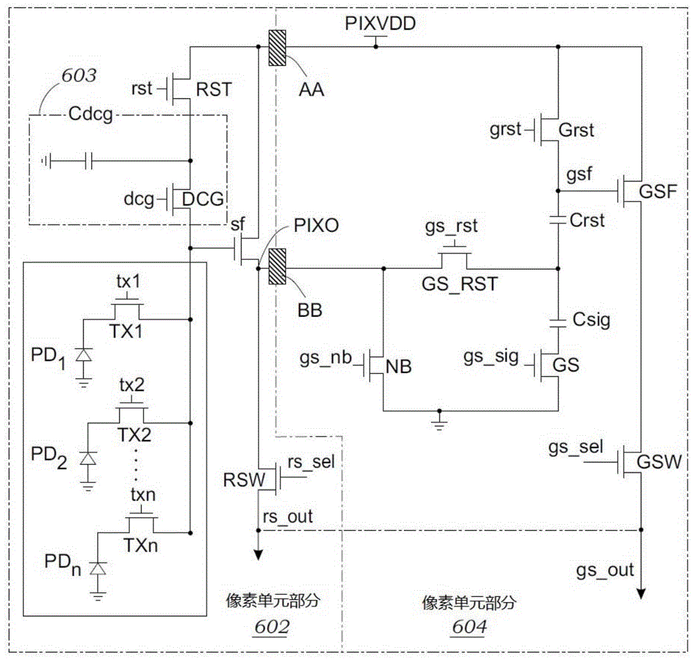
图6是根据本发明第一实施例的图5中所示的像素单元的电路图;FIG. 6 is a circuit diagram of the pixel unit shown in FIG. 5 according to the first embodiment of the present invention;
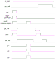
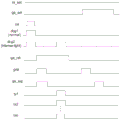
图7A是根据本发明第一实施例的图5中所示的控制信号时序用于执行可选读出模式的像素单元的时序控制图;7A is a timing control diagram of the control signal timing shown in FIG. 5 for performing the optional readout mode of the pixel unit according to the first embodiment of the present invention;
图7B是根据本发明第一实施例的图5中所示的另一控制信号时序用于执行可选读出模式的像素单元的时序控制图;7B is a timing control diagram of another control signal timing shown in FIG. 5 for performing a selectable readout mode of a pixel unit according to the first embodiment of the present invention;
图8是根据本发明第一实施例的图5中所示的控制信号时序用于执行另一可选读出模式的像素单元的时序控制图;FIG. 8 is a timing control diagram of the control signal timing shown in FIG. 5 for performing another optional readout mode of the pixel unit according to the first embodiment of the present invention;
图9是根据本发明第二实施例的像素单元的分解图;9 is an exploded view of a pixel unit according to a second embodiment of the present invention;
图10是根据本发明第二实施例的图9中所示的像素单元的电路图;及10 is a circuit diagram of the pixel unit shown in FIG. 9 according to a second embodiment of the present invention; and
图11是根据本发明第二实施例的图9中所示的控制信号时序用于执行可选读出模式的像素单元的时序控制图。FIG. 11 is a timing control diagram of the control signal timing shown in FIG. 9 for performing the optional readout mode of the pixel unit according to the second embodiment of the present invention.
具体实施方式Detailed ways
结合上述各个附图对本发明进一步进行图示描述。本发明为具有信号动态范围增强组件和可选滚动曝光和全局曝光读出模式及全局曝光读出路径中像素内相关双采样的堆叠图像传感器像素单元。本发明给出了堆叠图像传感器的各种实施例。在以下描述中,给出了大量细节描述用于理解本发明内容。本领域技术人员应当得知,本发明所记载的技术内容在没有具体细节或其他方法,组件,材料等的情况下可以得到实施。在其他情况下,已知的结构,材料或操作未呈现或在细节中描述,以避免模糊特定的内容。一个基底可具有一个正面和一个背面。任何加工过程从正面的执行操作可看作为正面操作,当从背面执行操作可被看作是背面操作。如光电二极管和相关的晶体管的结构和装置可形成在半导体基底的正面表面。包括金属布线层和导电层的交互层介质堆叠可形成在基底的正面表面。在一堆叠芯片设置中,既然每个芯片上的互连大都设置在每个芯片的正面,两个芯片的正面可直接连接。当特定电路元件位于或形成于一个基底上时,一般可认为是该电路位于基底的正面。The present invention will be further described with reference to the above-mentioned figures. The present invention is a stacked image sensor pixel unit with signal dynamic range enhancement components and optional rolling exposure and global exposure readout modes and intra-pixel correlated double sampling in the global exposure readout path. The present disclosure presents various embodiments of stacked image sensors. In the following description, numerous detailed descriptions are given for an understanding of the present invention. Those skilled in the art should know that the technical contents described in the present invention can be implemented without specific details or other methods, components, materials, etc. In other instances, well-known structures, materials or operations are not shown or described in detail in order to avoid obscuring specific content. A substrate can have a front side and a back side. Any machining process performed from the front side can be considered a front side operation, and when performed from the back side it can be considered a back side operation. Structures and devices such as photodiodes and related transistors may be formed on the front surface of the semiconductor substrate. An alternating layer dielectric stack including metal wiring layers and conductive layers can be formed on the front surface of the substrate. In a stacked chip setup, since the interconnects on each chip are mostly located on the front side of each chip, the front sides of the two chips can be directly connected. When certain circuit elements are located or formed on a substrate, the circuit is generally considered to be located on the front side of the substrate.
本专利所使用的“耦接”或“连接”定义如下。“连接”用于描述为两个电路元件之间的直连,例如,按照普通的集成电路加工技术形成的金属线。相比之下,“耦接”用于描述两个电路元件之间或者直连或者非直连。例如,两个耦接元件可以用金属线直接连接,或通过中间的电路元件(例如,电容,电阻,或晶体管的源/漏端)非直接连接。本发明的堆叠芯片排列中,既然每个芯片上的电互连点大多数形成在每个芯片的正面,两个芯片的正面可直接连接起来。当特定电路元件位于基底内或形成在基底上时,一般可看作是位于所述基底的正面。"Coupled" or "connected" as used in this patent is defined as follows. A "connection" is used to describe a direct connection between two circuit elements, eg, metal lines formed in accordance with common integrated circuit fabrication techniques. In contrast, "coupled" is used to describe either a direct or indirect connection between two circuit elements. For example, the two coupling elements may be directly connected by metal lines, or indirectly connected by intervening circuit elements (eg, capacitors, resistors, or source/drain terminals of transistors). In the stacked chip arrangement of the present invention, since most of the electrical interconnection points on each chip are formed on the front side of each chip, the front sides of two chips can be directly connected. When a particular circuit element is located in or formed on a substrate, it can generally be considered to be located on the front side of the substrate.
图1是一图像系统100的结构图。该图像系统100包括一具有多个图像传感器像素的像素阵列102,所述像素阵列包含多个具有本发明所提供的技术特征的图像传感器像素。如图中所示,图像系统100包括连接到控制电路108和读出电路104的像素阵列102,读出电路104连接到功能逻辑单元106。控制电路108和读出电路104连接到状态存储器110。在一实施中,像素阵列102为如图所示的图像传感器像素(例如,像素P1,P2…)的二维(2D)阵列。如图所示,每一像素排成行(例如,行R1到Ry)和列(例如,列C1到Cx)以获得一个人或地方或物体等的图像数据,由此可产生一个人或地方或物体的两维图像。在一实施例中,每一像素获取图像数据或图像电荷后,图像数据采用状态寄存器110指定读出模式的读出电路104读出,然后传输到功能逻辑单元106。在各种应用例中,读出电路104可包括放大电路,模数转换(ADC)电路,及其他。状态寄存器110可包括有程序化选择系统用以确定读出系统是通过滚动曝光还是全局曝光模式读出。功能逻辑单元106可仅存储图像数据或通过图像效果应用甚至处理图像数据(例如,裁剪,旋转,去红眼,调整亮度,调整对比度,或其他)。在一应用例中,读出电路104可沿读出列线(如图所示)一次读出一行图像数据,或者可采用各种其他技术(未示出)读出图形数据,例如串行读出或同时并行读出所有的像素。在一应用例中,控制电路108连接到像素阵列102以控制像素阵列102的可操作特性。控制电路108的操作可通过状态寄存器110的当前设置确定。例如,控制电路108可产生一快门信号用于控制图像获取。在一应用例中,此快门信号是一全局曝光信号使得像素阵列102的所有像素通过单一获取窗口同时分别获取它们的图像数据。在另一应用例中,此快门信号是一滚动曝光信号,每一像素行,列或组通过连续获取窗口连续实现。FIG. 1 is a structural diagram of an
图2是现有技术中具有滚动曝光读出模式的堆叠图像传感器像素单元的一实施例的电路图。该图和实施例用于简单描述本发明实施例像素的预期操作。如图所示,每一传感器像素200包括一光电二极管210(例如,光感器件)和像素支持电路211。光电二极管210可为现有CMOS图像传感器中采用的钉扎(Pinned)二极管。光电二极管210可设置在堆叠系统的传感器芯片上,像素支持电路211可设置在一单独的电路芯片上。在一应用例中,像素支持电路211包括一复位晶体管220,源极跟随(SF)晶体管225,及行选择晶体管230的电路芯片上,连接到如图所示的堆叠芯片系统的传感器芯片上的垂直通道传输晶体管215和光电二极管210。在另一应用例中,未标示出,像素支持电路包括电路芯片上的行选择晶体管230连接到堆叠系统的传感器芯片上的复位晶体管220,源极跟随(SF)晶体管225,和垂直通道传输晶体管215和光电二极管210。在操作过程中,在曝光期间光电二极管210产生电荷响应入射光。垂直通道传输晶体管215响应传输控制信号TX将光电二极管累积的电荷传输到浮动扩散点(FD)217。当光电二极管210是垂直通道传输晶体管215的源极时,浮动扩散点217是传输晶体管的实际上的漏极。在一实施例中,垂直通道传输晶体管是一垂直通道金属氧化物半导体场效应管(MOSFET)。复位晶体管220连接于电源VDD和浮动扩散点217之间,响应于复位控制信号RST,复位传感器像素200(例如,放电或充电浮动扩散点217和光电二极管210到当前电压)。浮动扩散点217连接到源极跟随晶体管225的栅极。源极跟随晶体管225连接于电源VDD和行选择晶体管230之间,放大输出浮动扩散点217的电压信号。行选择晶体管230根据行选择控制信号RS将像素电路的输出从源极跟随晶体管225输出到读出列,或位线235。光电二极管210和浮动扩散点217由暂时有效的复位信号RST和传输控制信号TX复位。累积窗口(例如曝光阶段)在传输控制信号TX失效时开始,使得入射光在光电二极管210累积产生电荷。当光电子在光电二极管210处累加,其电压降低(电子带负电荷)。在曝光期间光电二极管210上的电压或电荷代表入射到光电二极管210上的光强度。在曝光期后,复位控制信号RST失效,关闭复位晶体管220并将浮动扩散点217与电源VDD隔离。传输控制信号TX有效,将光电二极管210连接到浮动扩散点217。电荷从光电二极管210通过垂直通道传输晶体管215传输到浮动扩散点217,在曝光期间使得浮动扩散点217的电压通过一定比例降低到光电二极管210累积的光电子。FIG. 2 is a circuit diagram of an embodiment of a stacked image sensor pixel cell with a rolling exposure readout mode in the prior art. This figure and example are used to briefly describe the intended operation of a pixel of an embodiment of the present invention. As shown, each
图像传感器的一个重要的设计要点是动态范围,它是由最大非饱和光电流和最小可测光电流之间的对数比所确定。对于具有固定饱和电荷的传感器,也是指性能,饱和度限制了其最高信号。一般地,最小可测光电流由光电二极管和浮动扩散的复位采样噪声确定。降低动态范围上的复位采样噪声的影响依赖于相关双采样(CDS)。CDS是选取像素信号的两个样本并从第二个信号减去第一个信号以去掉复位采样噪声。一般地,采样一般快速跟随光电二极管和浮动扩散点的复位执行一次且在光电二极管允许累积电荷并将其传输到浮动扩散点后执行一次。信号相减的操作在像素的外围电路执行且可能增加传统的图像传感器的面积虽然不一定是像素的面积。使用滚动曝光模式的图像传感器可包含仅增加外围电路元件的CDS且像素中没有增加的其他电路元件。使用全局曝光模式的图像传感器像素内可能需要多个电容和晶体管,这些降低了填充因子。通过分开CDS所需的增加组件到电路芯片上以保持降低填充因子从而分离并堆叠在传感器芯片上部。An important design point for image sensors is dynamic range, which is determined by the logarithmic ratio between the maximum unsaturated photocurrent and the minimum measurable photocurrent. For sensors with a fixed saturation charge, also referring to performance, saturation limits its maximum signal. Typically, the minimum measurable photocurrent is determined by the reset sampling noise of the photodiode and floating diffusion. The effect of reducing reset sampling noise on the dynamic range relies on correlated double sampling (CDS). CDS takes two samples of the pixel signal and subtracts the first signal from the second signal to remove reset sampling noise. In general, sampling is performed once quickly following the reset of the photodiode and floating diffusion and once after the photodiode has allowed charge to accumulate and transfer to the floating diffusion. The signal subtraction operation is performed in peripheral circuits of the pixel and may increase the area of a conventional image sensor although not necessarily the area of the pixel. An image sensor using a rolling exposure mode may include only the addition of the CDS of peripheral circuit elements and no other circuit elements added in the pixel. Multiple capacitors and transistors may be required within an image sensor pixel using the global exposure mode, which reduces the fill factor. The additional components required for the CDS are separated and stacked on top of the sensor chip by separating the additional components required for the CDS onto the circuit chip to keep the fill factor low.
图3A为现有技术普通像素单元的布局图。光电二极管310,传输晶体管315和像素电路311占用相同的半导体芯片。图3B为图3A中所示的像素单元沿AA’的截面图。光电二极管310和像素电路311相应于图2中的标示为光电二极管210和像素电路211的光电二极管和像素电路,除了他们占用相同的芯片晶片。传输晶体管315占用如图2中的传输晶体管215相同的位置,除了传输晶体管315为一普通意义上的平面互补金属氧化物半导体场效应管(CMOSFET),它的源极,通道,及漏极位于半导体基底内,且并行与半导体基底的表面。图3A和图3B中所示的M1尽可能减少对降低像素阵列尺寸和生产成本是有利的。然而芯片尺寸M1受加工技术的最小化设计规则的需求所限,比如设置像素电路311到传输晶体管315最接近的方式。这种情况是迫使像素单元分离到两个堆叠芯片的主要因素,芯片的像素电路可堆叠在光电二极管和传输晶体管上以降低M1的晶片尺寸。FIG. 3A is a layout diagram of a common pixel unit in the prior art. The
图4A是现有技术中普通像素单元布局的分解图。其中,光电二极管410和平面互补CMOSFET传输晶体管415位于传感器芯片的半导体基底上,且像素电路411位于电路半导体芯片一隔开的基底上。图4A呈现了传感器芯片的分解图,它的组件置于上部表面,对齐排列于组件置于下部表面电路芯片,通过芯片内互连440连接。在图4B中,电路芯片的下面实际上是前面所述的基底的前面。图4B为图4A像素单元沿BB’包括电路芯片的叠加部分的截面图。图4B呈现了由芯片内互连440连接的两堆叠半导体芯片。与图3A和图4A相比,本领域技术人员应该意识到,假设光电二极管310和410具有相同的尺寸,芯片尺寸M2比M1小,这样能提供降低生产加工成本的可能。4A is an exploded view of a conventional pixel cell layout in the prior art. Among them, the
在图4A和图4B中所示的堆叠组件中,芯片尺寸限制由传感器芯片确定。假设期望保留光电二极管的尺寸,进一步降低芯片尺寸的机会是降低传输晶体管尺寸,或重置其在光电二极管的覆盖空间。In the stacked assembly shown in Figures 4A and 4B, the chip size limit is determined by the sensor chip. Assuming it is desired to preserve the size of the photodiode, the opportunity for further chip size reduction is to reduce the pass transistor size, or reset its footprint in the photodiode.
先进的图像传感器中,降低噪音方法的使用不足以增加动态范围以获取明亮的太阳光及暗影存在的户外场景。先进的动态范围增强技术可采用性能调整方案。此种方案中,在光电二极管电荷传输到浮动节点过程中,性能增强一次或多次。这种使用在小面积堆叠图像传感器像素的动态范围增强方案是本发明所描述的重点部分。本发明实施方案中采用的动态范围增强方案包含通过在具有传感器芯片上的浮动节点的平行结构中增加电容和电容控制晶体管来构建性能调整电路。通过连接所添加的电容到浮动节点,光电二极管电荷传输到一个较大的电容产生较低的转换增益,以及在饱和之前累积更多的电荷。这种性能用于高光照度下成像的场景而不是正常的或低光照度下成像的场景中。因此这种方案所需要的特征是增加一个电容控制晶体管和一个关闭像素(off pixel)电容控制晶体管控制信号电路以感知成像场景的光照度。各种感知场景光强度和基于其上的信号控制电路以采用所期望信号到信号增强电容控制晶体管的栅极的方法是本领域技术人员所熟知的内容,此处不做赘述。In advanced image sensors, the use of noise reduction methods is not sufficient to increase the dynamic range for outdoor scenes with bright sunlight and dark shadows. Advanced dynamic range enhancement techniques enable performance tuning schemes. In this scheme, the performance is enhanced one or more times during the transfer of the photodiode charge to the floating node. This dynamic range enhancement scheme using stacked image sensor pixels in a small area is the focus of this description. The dynamic range enhancement scheme employed in embodiments of the present invention involves building a performance tuning circuit by adding capacitance and capacitance control transistors in a parallel structure with floating nodes on the sensor chip. By connecting the added capacitor to the floating node, the photodiode charge is transferred to a larger capacitor resulting in lower conversion gain and more charge accumulation before saturation. This performance is used for scenes imaged in high light rather than normal or low light. Therefore, the required feature of this scheme is to add a capacitor control transistor and an off pixel capacitor control transistor control signal circuit to sense the illumination of the imaging scene. Various methods of sensing the light intensity of the scene and controlling the circuit based on the signal to adopt the desired signal to the gate of the signal-enhancing capacitor control transistor are well known to those skilled in the art, and will not be repeated here.
图5是根据本发明第一实施例的像素单元的分解图。图5呈现了像素单元布局,其中像素单元部分502包括光电二极管PDa,PDb,PDc,PDd及各自的MOSFET传输晶体管TXa,TXb,TXc,TXd和一般连接的浮动节点FN位于传感器芯片510的半导体基底上。像素单元部分502还包括复位晶体管RST和放大晶体管SF及动态范围增强电容Cfd和位于传感器芯片内的电容控制晶体DCG,用于当选择滚动曝光模式时用于转换图像电荷到图像信号并通过行选择晶体管RSW从传感器芯片将图像信号连接输出。图5还呈现了包含位于电路芯片511的独立半导体基底上的像素电路的像素单元部分504(像素电路芯片)。图5呈现了传感器芯片510的分解图且它的组件位于上部表面以芯片内互连AA和BB对齐排列到组件位于下面或前述所定义的正面的电路芯片511。文中未给出但可容易想象到类似于图4B的一个附图且可呈现如图5中所示的两堆叠半导体芯片,通过芯片内互连AA和BB连接。5 is an exploded view of a pixel unit according to the first embodiment of the present invention. FIG. 5 presents a pixel cell layout in which
像素单元部分502呈现了仅像素相关组件位于传感器芯片510上。像素单元部分502重复形成图像阵列的行和列。传感器芯片510可包含额外的外围电路作为功能化图像传感器的图像阵列部分的需求,例如,连接复位控制信号和传输晶体管的传输控制信号到所有的像素单元。光电二极管PDa,PDb,PDc和PDd可以是相同的尺寸和位置,例如图中所示2×2的阵列。典型地,像素单元部分502内光电二极管的尺寸和位置是选定的,如像素单元部分502的阵列的所有光电二极管设置为统一的样式布局。在实例中,像素单元502用于形成彩色图像传感器。各种颜色的滤光器可设置在入射光路径内的每一像素位置处。一种已知的2×2的滤光器安置是拜尔滤光模式(Bayer filter pattern),其包含一个红色,一个蓝色,及两个绿色滤光器(RGGB)。位于像素单元部分504上的像素电路限制其占用不多于像素单元部分502所占用的面积。如图5中所示,像素电路芯片504(像素电路芯片)包括当选择全局曝光模式时提供全局曝光模式功能的读出电路。像素电路芯片511可包含额外的外围电路作为功能化图像传感器的像素电路部分的需求,例如,连接控制信号和电源。
图6是图5中所示的根据本发明第一实施例的像素单元的电路图。图6中的像素单元部分602和604相应于图5中的像素单元部分502和504。图6中所示的电路图更清晰地呈现了各器件之间的连接关系。器件名称在两个图中是通用的且用于描述像素单元的操作。图6中设置了传输晶体管(TXa,TXb,TXc,TXd),每一晶体管分别连接到单独的光电二极管(PDa,PDb,PDc,PDd)并共享浮动节点FN,表示为像素单元部分602且设置于第一基底内用以累积和传输图像电荷以响应入射到光电二极管上的光。在图6中,光电二极管和它们各自的传输晶体管作为单元1,2…n列出而不是图5中所示的a,b,c…。这主要是为了体现本发明电路可以是多个光电二极管和传输晶体管,而不是图5中所示的四组光电二极管和传输晶体管。一复位晶体管RST和放大晶体管SF位于像素单元部分602上并设置在第一基底内,用于转换图像电荷到图像信号(PIXO)及一行选择晶体管(RSW)用于当选择滚动曝光模式时从像素单元部分602将图像信号输出。一动态范围增强电容Cdcg和电容控制晶体DCG设置在像素单元部分602上,在高光照成像场景中用于提供动态范围增强模式。图6还描述了像素单元604的读出电路块,且设置在堆叠在第一基底正面上的第二基底内,其中读出电路块包括一个可选的全局曝光模式。图6中还呈现了芯片内互连AA和BB直连放大晶体管SF到全局曝光模式读出电路块。芯片内互连BB连接产生于源极放大器SF源极的图像信号PIXO到第二基底上的像素单元部分604内全局曝光模式读出路径。芯片内互连AA连接电源PIXVDD到复位晶体管RST和放大晶体管SF。FIG. 6 is a circuit diagram of the pixel unit shown in FIG. 5 according to the first embodiment of the present invention. The
本发明的一个发明点是提供现有技术之上包含名称为603的像素单元,当成像场景为高光照度情况时,所述图像电荷部分通过电容控制晶体管DCG储存在动态范围增强电容Cdcg上。动态范围增强电容Cdcg连接在地和复位晶体管RST及电容控制晶体管DCG的连接点处,可以为MOS电容,能提供较好的像素输出电压线性,或者为二极管电容用于电荷整合。An inventive point of the present invention is to provide a pixel unit named 603 above the prior art. When the imaging scene is high illumination, the image charge is partially stored on the dynamic range enhancement capacitor Cdcg through the capacitor control transistor DCG. The dynamic range enhancement capacitor Cdcg is connected to the ground and the connection point of the reset transistor RST and the capacitance control transistor DCG, and can be a MOS capacitor to provide better linearity of pixel output voltage, or a diode capacitor for charge integration.
本发明还提供一现有技术基础上的创新的像素单元,其图像信号可选地通过设置在第一基底上的电路以滚动曝光模式输出或可选地通过设置在第二基底上的电路以全局曝光模式输出。以滚动曝光读出模式产生图像且不需要信号穿过第二基底,能降低功耗和信噪以及增加帧率。进一步从第一基底电路分离出第二基底电路利于从独立设置在第一基底的可选源中提供电源PIXVDD。The present invention also provides an innovative pixel unit based on the prior art, the image signal of which is optionally output in a rolling exposure mode through a circuit disposed on the first substrate or alternatively through a circuit disposed on the second substrate to Global exposure mode output. Generating images in a rolling exposure readout mode without requiring the signal to pass through the second substrate can reduce power consumption and signal-to-noise as well as increase frame rates. Further separating the second substrate circuit from the first substrate circuit facilitates supplying the power supply PIXVDD from an optional source provided independently on the first substrate.
为读出滚动曝光模式中的图像信号PIXO,仅需行选择晶体管RSW传输读信号rs_pix到off_pixel读出电路。因此在滚动曝光模式的选择上,通过在图1中所示的状态寄存器110上的设置,控制电路108可至少对图6中的晶体管GS_RST,Grst,GSF及GSW关闭。图7A给出了用于执行从像素单元部分602的图像信号PIXO的滚动曝光模式读出的控制时序。图7A中的每一控制信号相应于图6中所示应用于相关晶体管门电极相似名称的信号及他们的相关状态开(高)/关(低)。此处包含两种电荷处理模式。一种是用于低于正常光照强度的成像场景,采用信号dcg1;另一种是用于高光照强度的成像场景,采用信号dcg2。在低光照强度成像场景中,为从像素单元部分602执行滚动曝光读出模式,时序如图7A所示。首先所有的信号处于关闭状态。接下来复位控制信号rst作用于复位晶体管RST上,且控制信号dcg作用于电容控制晶体管DCG使其设置为高,拉高浮动节点FND到初始电压值VFN0(接近于PIXVDD)且将放大器SF的源极的电压拉至相应于初始电压值VFN0的图像信号PIXO(rst)。然后行选择晶体管RSW打开,初始图像信号以电压值Vrs_pix0传输到节点rs_pix。复位晶体管RST和电容控制晶体DCG置低电平,随后传输晶体管TX1置为高电平。传输晶体管TX1保持高电平一段时间(曝光时间),然后置为低电平。在曝光期间,浮动节点FN充电到与入射到光电二极管PD1(此处称VFN1)的光照强度成一定比例,其充电放大晶体管SF的栅极,以将放大晶体管SF的源极拉至相应于VFN1的图像信号,且行选择晶体管RSW保持打开状态,图像信号以电压值Vrs_pix1传输到节点rs_pix。读出电路不在像素单元部分602(off-pixel)上但在图像传感器的其他处,对图像信号Vrs_pix0和Vrs_pix1执行相关双采样(CDS)。图7A的最后一行给出了当复位晶体管RST关闭且传输晶体管TXa打开和关闭前和后的off-pixel CDS电路采样信号rs_pix。图像信号Vrs_pix1减去图像信号Vrs_pix0能够提供低噪声信号到光电二极管PD1相应的图像传感器。读出相似的光电二极管PD2…及PDn信号以完成像素单元部分602的图像信号。To read out the image signal PIXO in the rolling exposure mode, only the row selection transistor RSW needs to transmit the read signal rs_pix to the off_pixel readout circuit. Therefore, in the selection of the rolling exposure mode, the
当高光照强度场景成像时,为执行从像素单元部分602以滚动曝光模式读出信号PIXO,可采用图7A中所示的时序。首先,所有信号处于关闭状态。接着,复位控制信号作用于复位晶体管RST且控制信号dcg置为高电平作用于电容控制晶体管DCG,将浮动节点FN拉至初始电压值VFN0(接近于PIXVDD)且将放大晶体管SF的源极拉至相应于初始电压值VFN0的图像信号PIXO(rst)。然后行选择晶体管RSW打开,初始图像信号以电压值Vrs_pix0传输到节点rs_pix。然后复位晶体管RST和电容控制晶体管DCG置为低电平。一小段时间后,电容控制晶体管DCG又置为高,同时传输晶体管TX1置为高电平。传输晶体管TX1保持高电平一段时间(曝光期间)然后置为低电平。在曝光期间,浮动节点FN和动态范围增强电容Cdcg充电到与光电二极管PD1(此处称VFN1)上光照强度成一定比例,对放大晶体管SF的栅极进行充电以将放大晶体管SF的源极拉至相应于VFN1的图像信号,行选择晶体管RSW保持打开状态,图像信号以电压Vrs_pix1传输到节点rs_pix。浮动节点FN和动态范围增强电容Cdcg的组合电容比浮动节点FN单独的电容大,在饱和前可以累积更多的电荷,像素单元动态范围因此加强。读出电路不在像素单元部分602(off-pixel)上单在图像传感器的其他处,对图像信号Vrs_pix0和Vrs_pix1执行相关双采样(CDS)。图7A的最后一行给出了相应图示。To perform the readout of the signal PIXO from the
图7B给出了另一控制信号时序用于执行可选读出模式的像素单元的时序控制图。与图7A给出的时序相比,此优选实施例中的时序只需实施一次曝光,分别读取高增益和低增益两种转换增益下的值,并通过帧合成获取高动态图像,此方式可实现更高的帧率。结合图6电路图,以光电二极管PD为四个为例,在此种模式下,信号grst、gs_rst、gs_sig、gs_nb、gs_sel恒为低电平。其具体的实施过程为:首先初始化所有光电二极管PD,信号rst,dcg,tx1置为高电平,Cdcg、FD和PD1端置为高电平。曝光开始,信号rst,dcg,tx1置为低电平,PD1曝光开始累积光电荷。开始读取,rs_sel选通,信号rst和dcg至高电平,初始化FN节点电位。置rst为低电平,读取此时低转换增益LCG的初始信号Vlcg0。置rst为高电平,FN节点电位再次重置至PIXVDD。信号rst和dcg置为低电平,读取高转换增益HCG时的初始信号Vhcg0。信号tx1置为高电平,TX1导通,将PD1累积的电子转移至FN节点。信号tx1置为低电平,读取高转换增益HCG时的信号电压值Vhcg1。信号tx1和dcg置为高电平,将PD1累积的电子重新分配至Cdcg和FN节点。信号tx1置低电平,读取低转换增益LCG时的信号电压Vlcg1。由此可计算得出高转换增益HCG模式下信号值Vhcg=Vhcg1-Vhcg0,低转换增益LCG模式下信号值Vlcg=Vlcg1-Vlcg0。重复上述实施过程,读取其他所有光电二极管的信号。高转换增益HCG和低转换增益LCG下的信号可合成高动态范围图像。FIG. 7B shows a timing control diagram of another control signal timing for a pixel cell performing an optional readout mode. Compared with the timing sequence given in FIG. 7A, the timing sequence in this preferred embodiment only needs to implement one exposure, read the values under the two conversion gains of high gain and low gain respectively, and obtain high dynamic images through frame synthesis. Higher frame rates can be achieved. Referring to the circuit diagram of FIG. 6 , taking four photodiodes PD as an example, in this mode, the signals grst, gs_rst, gs_sig, gs_nb, and gs_sel are always at low level. The specific implementation process is as follows: firstly, all photodiodes PD are initialized, the signals rst, dcg, and tx1 are set to high level, and the terminals of Cdcg, FD and PD1 are set to high level. Exposure starts, the signals rst, dcg, tx1 are set to low level, and PD1 exposure starts to accumulate photocharges. To start reading, rs_sel is gated, the signals rst and dcg are brought high, and the FN node potential is initialized. Set rst to a low level, and read the initial signal Vlcg0 of the low conversion gain LCG at this time. By setting rst high, the FN node potential is reset to PIXVDD again. The signals rst and dcg are set low, and the initial signal Vhcg0 is read at the high conversion gain HCG. The signal tx1 is set to a high level, TX1 is turned on, and the electrons accumulated by PD1 are transferred to the FN node. The signal tx1 is set to a low level, and the signal voltage value Vhcg1 when the high conversion gain HCG is read is read. Signals tx1 and dcg are asserted high, redistributing electrons accumulated by PD1 to the Cdcg and FN nodes. The signal tx1 is set to a low level, and the signal voltage Vlcg1 when the low conversion gain LCG is read is read. From this, it can be calculated that the signal value Vhcg=Vhcg1-Vhcg0 in the high conversion gain HCG mode, and the signal value Vlcg=Vlcg1-Vlcg0 in the low conversion gain LCG mode. Repeat the above implementation process to read the signals of all other photodiodes. Signals at high conversion gain HCG and low conversion gain LCG can synthesize high dynamic range images.
从像素单元部分604上的电路所提供的具有像素内CDS的像素单元部分602中以全局曝光模式读出图像信号的操作规则包含两个阶段,为采样复位值和采样信号值。在第二个阶段(采样信号值),像素内CDS操作根据像素单元部分604上的电路元件结构特性自动发生。具体操作上,为读出全局曝光模式的图像信号PIXO,像素单元部分604上的所有晶体管都可操作以传输读信号rs_pix到off_pixel读出电路。因此通过对图1中所示的状态寄存器110合适的设置的选择,控制电路108可关闭晶体管RSW。图8给出的控制时序用于执行图像信号PIXO的全局曝光模式从像素单元部分602读出。图8中所示的每一控制信号相应于图6中所示的相关晶体管的相应名称的门极信号,以及他们相关的状态开(高)/关(低)。为执行从像素单元部分602全局曝光方式读出的图像信号PIXO,图8中给出了低于正常或正常的光照强度场景中成像的控制时序。首先复位控制信号rst作用于复位晶体管RST,且控制信号dcg1作用于电容控制晶体管DCG将其置为高电平,以拉高浮动节点FN到初始电压值VFN0(接近于电压值PIXVDD),且将放大晶体管SF源极拉至相应于初始电压值VFN0的图像信号PIXO(rst)。当晶体管Grst,GS,及GS_RST置为高片以对电容Crst充电至电压V(Crst),V(Crst)=PIXVDD-PIXO(rst),设置RST和DCG为低电平。全局曝光复位晶体管Grst关闭允许电容Crst的顶部极板浮动。然后所有的传输晶体管TX1,TX2…TXn打开,且允许持续曝光时间的时段。若成像场景是高光照强度的场景,控制信号序列dcg2会替代信号序列dcg1从而打开电容控制晶体管DCG和导致浮动节点的电容及饱和前图像电荷累积数量的增加的传输晶体管保持一致。这使得图像信号PIXO(sig)对动态范围增强电容Csig充电到与光电二极管上光照强度成一定比例。全局曝光传输晶体管GS关闭,GS_RST随后关闭,使得图像信号PIXO(sig)保留在电容Csig上。目前所描述的信号序列,在像素内CDS发生在复位和到电容的图像信号的顺序使用的过程时,完成将全局曝光图像信号存储到全局曝光电容。The operating rule for reading out the image signal in the global exposure mode from the
为了从全局曝光的电容中读出图像信号,图8进一步给出下述增加的步骤顺序。接下来全局曝光复位晶体管Grst打开预充电容Crst的寄生电容。当Grst打开且关闭之前很短时间内,全局曝光行选择晶体管GSW设置为打开以从放大器GSF采样复位信号作为信号Vgs_pix0直到全局曝光复位晶体管Grst关闭。全局曝光复位晶体管Grst关闭之后,全局曝光行选择晶体管GSW保持打开,下一步打开全局曝光传输晶体管GS一段时间以从放大器GSF采样图像信号Vgs_pix1。行选择晶体管GSW然后关闭。读出电路不在像素单元部分604(off-pixel)上但在图像传感器的其他处,对图像信号Vrs_pix0和Vrs_pix1执行相关双采样(CDS)。当复位晶体管Grst关闭及传输晶体管开或关的前后时间,像素单元部分604(off-pixel)CDS电路采样信号gs_pix。增加的操作处理源跟随放大器晶体管GSF的噪声。In order to read out the image signal from the globally exposed capacitance, Figure 8 further presents the following incremental sequence of steps. Next, the global exposure reset transistor Grst turns on the parasitic capacitance of the precharge capacitor Crst. Shortly before Grst turns on and turns off, the global exposure row select transistor GSW is set on to sample the reset signal from the amplifier GSF as the signal Vgs_pix0 until the global exposure reset transistor Grst turns off. After the global exposure reset transistor Grst is turned off, the global exposure row select transistor GSW is kept on, and the global exposure transfer transistor GS is next turned on for a period of time to sample the image signal Vgs_pix1 from the amplifier GSF. The row select transistor GSW is then turned off. The readout circuitry, not on the pixel cell portion 604 (off-pixel) but elsewhere on the image sensor, performs correlated double sampling (CDS) on the image signals Vrs_pix0 and Vrs_pix1. The pixel cell portion 604 (off-pixel) CDS circuit samples the signal gs_pix when the reset transistor Grst is turned off and the transfer transistor is turned on or off. The added operational processing source follows the noise of the amplifier transistor GSF.
图6中所示的读出电路增加的特征包括rs_out和gs_out信号节点连接到一起以减少电路连线。发明内容中描述的其他部分保持不变。The added features of the readout circuit shown in Figure 6 include the rs_out and gs_out signal nodes being connected together to reduce circuit wiring. The rest of the description in the Summary of the Invention remains unchanged.
图9是根据本发明第二实施例的像素单元的分解图,相关标示同图5中所示。图10是图9中所示的像素单元的电路图。图9和图10中所示的本发明第二实施例与图5和图6总所示的第一实施不同,全局曝光传输晶体管GS位于电容Crst和Csig之间而非图5和图6中所示在电容Csig和地之间。基于滚动曝光读出模式,图像信号如上述本发明第一实施例所述的读出方式。基于全局曝光读出模式,图像信号读出方式类似于上述第一实施例中所述,除了图11中所示的几步。FIG. 9 is an exploded view of a pixel unit according to a second embodiment of the present invention, and the related symbols are the same as those shown in FIG. 5 . FIG. 10 is a circuit diagram of the pixel unit shown in FIG. 9 . The second embodiment of the present invention shown in FIGS. 9 and 10 differs from the first implementation generally shown in FIGS. 5 and 6 in that the global exposure pass transistor GS is located between capacitances Crst and Csig instead of in FIGS. 5 and 6 Shown between capacitor Csig and ground. Based on the rolling exposure readout mode, the image signal is read out as described in the first embodiment of the present invention. Based on the global exposure readout mode, the image signal readout manner is similar to that described in the above-described first embodiment, except for the steps shown in FIG. 11 .
图10中所示的读出电路的附加特性包括rs_out和gs_out信号节点可连接到一起以减少电路连线。发明内容中描述的其他部分不变。Additional features of the readout circuit shown in Figure 10 include that the rs_out and gs_out signal nodes can be connected together to reduce circuit wiring. Other parts described in the summary of the invention remain unchanged.
本专利实施方案中“一个实施例”,“一个应用例”或“一个例子”等,意思为本实施例中特定的特征,结构,或特点,或者包含在根据本发明的至少一个例子中。因此,“在一个实施例中”或“在一个例子中”的短语出现在本说明书的各种地方,不必限于参考相同的具体实施方案或实施例。而且,独特的特征,结构或特点可包含在一个或多个实施例的任何合适的方式中。定向术语,例如“上”,“下”,“之上”,“之下”,用于参考图中描述的定位。而且,术语“有”,“包含”,“特定”,及类似术语,除非有特定说明,都定义为“包含”。特点,结构或特征可包含在集成电路中,电路中,组合的逻辑电路中,或其他适用的组件,以提供所述的功能性。另外,此处提出的附图是为本领域技术人员提供解释说明且这些附图没必要按比例画出。"One example", "one application example" or "one example" etc. in the embodiments of this patent means a specific feature, structure, or characteristic of this example, or included in at least one example according to the present invention. Thus, the appearances of the phrases "in one embodiment" or "in an example" in various places in this specification are not necessarily limited to reference to the same specific embodiment or example. Furthermore, the unique features, structures or characteristics may be incorporated in any suitable manner in one or more embodiments. Orientation terms, such as "upper", "lower", "above", "below", are used to refer to the orientations described in the figures. Also, the terms "have", "includes", "in particular", and similar terms, are defined as "including" unless specifically stated otherwise. Features, structures or characteristics may be incorporated into integrated circuits, circuits, combinational logic circuits, or other suitable components to provide the described functionality. In addition, the drawings presented herein are provided for the purpose of illustration for those skilled in the art and are not necessarily drawn to scale.
本发明上述给出的示例,包括在摘要中描述的,并不详尽或限定于精确的形式披露。本发明所述的详细的实施例,例子,是为了说明的目的,在不背离本发明更广泛的主旨和范围下,不同形式的等效修改是可能的。确实,根据本发明提供的特定的实施例的结构和材料用于说明的目的且其他结构和材料也可应用于其他实施例中及例子中。根据上述详细的说明可对本发明实施例进行修改。用于权利要求中的术语不应解释为限定于本发明具体实施内容和权利要求部分中所揭露的具体实施例。相反地,权利要求中完整确定的范围应解释为根据权利要求解释确立的声明。本发明的说明书和附图应被看作是解释性的,而不是约束性的。The examples of the invention given above, including those described in the Abstract, are not intended to be exhaustive or limited to the precise form disclosed. The detailed embodiments, examples, and examples of this invention are described for purposes of illustration, and various forms of equivalent modification are possible without departing from the broader spirit and scope of the invention. Indeed, the structures and materials of the specific embodiments provided in accordance with this disclosure are provided for illustrative purposes and other structures and materials may also be employed in other embodiments and examples. Modifications may be made to the embodiments of the present invention in light of the foregoing detailed description. The terms used in the claims should not be construed to be limited to the specific embodiments disclosed in the Detailed Description and the Claims Section. Rather, the scope fully established in the claims should be construed as the statements established by the interpretation of the claims. The specification and drawings of the present invention are to be regarded in an illustrative rather than a restrictive sense.
Claims (15)
Applications Claiming Priority (4)
| Application Number | Priority Date | Filing Date | Title |
|---|---|---|---|
| US15/424,124 US9992437B1 (en) | 2017-02-03 | 2017-02-03 | Stacked image sensor pixel cell with in-pixel vertical channel transfer transistor |
| US15/424,124 | 2017-02-03 | ||
| US15/678,438 | 2017-08-16 | ||
| US15/678,438 US10070081B2 (en) | 2017-02-03 | 2017-08-16 | Stacked image sensor pixel cell with dynamic range enhancement and selectable shutter modes and in-pixel CDS |
Publications (2)
| Publication Number | Publication Date |
|---|---|
| CN108200367A CN108200367A (en) | 2018-06-22 |
| CN108200367B true CN108200367B (en) | 2020-09-18 |
Family
ID=62592256
Family Applications (1)
| Application Number | Title | Priority Date | Filing Date |
|---|---|---|---|
| CN201810099793.5A Active CN108200367B (en) | 2017-02-03 | 2018-01-31 | Pixel unit, method for forming pixel unit and digital camera imaging system assembly |
Country Status (2)
| Country | Link |
|---|---|
| US (1) | US10070081B2 (en) |
| CN (1) | CN108200367B (en) |
Families Citing this family (59)
| Publication number | Priority date | Publication date | Assignee | Title |
|---|---|---|---|---|
| US10686996B2 (en) | 2017-06-26 | 2020-06-16 | Facebook Technologies, Llc | Digital pixel with extended dynamic range |
| US10598546B2 (en) | 2017-08-17 | 2020-03-24 | Facebook Technologies, Llc | Detecting high intensity light in photo sensor |
| CN108270981B (en) * | 2017-12-19 | 2021-05-14 | 思特威(上海)电子科技股份有限公司 | Pixel unit, imaging method and imaging device thereof |
| US11658193B2 (en) | 2018-01-23 | 2023-05-23 | Samsung Electronics Co., Ltd. | Image sensor |
| US10714517B2 (en) * | 2018-01-23 | 2020-07-14 | Samsung Electronics Co., Ltd. | Image sensor |
| US10670526B2 (en) * | 2018-03-05 | 2020-06-02 | Smartsens Technology (Cayman) Co., Limited | DNA sequencing system with stacked BSI global shutter image sensor |
| US11004881B2 (en) * | 2018-04-03 | 2021-05-11 | Facebook Technologies, Llc | Global shutter image sensor |
| US12015862B2 (en) | 2018-05-24 | 2024-06-18 | Gigajot Technology, Inc. | Image sensor having pixels with isolated floating diffusions |
| US11906353B2 (en) | 2018-06-11 | 2024-02-20 | Meta Platforms Technologies, Llc | Digital pixel with extended dynamic range |
| US11463636B2 (en) | 2018-06-27 | 2022-10-04 | Facebook Technologies, Llc | Pixel sensor having multiple photodiodes |
| US10897586B2 (en) | 2018-06-28 | 2021-01-19 | Facebook Technologies, Llc | Global shutter image sensor |
| EP3605606B1 (en) * | 2018-08-03 | 2022-06-15 | ams Sensors Belgium BVBA | Imaging system comprising an infrared light source and an image sensor |
| US10931884B2 (en) | 2018-08-20 | 2021-02-23 | Facebook Technologies, Llc | Pixel sensor having adaptive exposure time |
| US11956413B2 (en) | 2018-08-27 | 2024-04-09 | Meta Platforms Technologies, Llc | Pixel sensor having multiple photodiodes and shared comparator |
| CN110383824B (en) * | 2018-10-09 | 2021-08-06 | 深圳市汇顶科技股份有限公司 | Image sensor, semiconductor structure, and method of operating an image sensor |
| WO2020073626A1 (en) * | 2018-10-09 | 2020-04-16 | Shenzhen GOODIX Technology Co., Ltd. | Image sensor with dynamic charge-domain sampling |
| US11595602B2 (en) | 2018-11-05 | 2023-02-28 | Meta Platforms Technologies, Llc | Image sensor post processing |
| US11431926B2 (en) * | 2018-11-09 | 2022-08-30 | Semiconductor Components Industries, Llc | Image sensors having high dynamic range imaging pixels |
| US11218660B1 (en) | 2019-03-26 | 2022-01-04 | Facebook Technologies, Llc | Pixel sensor having shared readout structure |
| CN111755466B (en) * | 2019-03-28 | 2023-06-16 | 群创光电股份有限公司 | electronic device |
| US11943561B2 (en) | 2019-06-13 | 2024-03-26 | Meta Platforms Technologies, Llc | Non-linear quantization at pixel sensor |
| CN114270808B (en) * | 2019-07-26 | 2024-11-29 | 苹果公司 | Pixel readout circuit with light intensity and contrast variation detection capability sharing photodetector |
| US11936998B1 (en) | 2019-10-17 | 2024-03-19 | Meta Platforms Technologies, Llc | Digital pixel sensor having extended dynamic range |
| CN112119624A (en) * | 2019-10-24 | 2020-12-22 | 深圳市大疆创新科技有限公司 | Image sensor, imaging device and mobile platform |
| US11152404B2 (en) * | 2019-12-20 | 2021-10-19 | Omnivision Technologies, Inc. | Tunnel contact for a pixel cell in an imaging system |
| KR102838191B1 (en) | 2020-02-10 | 2025-07-25 | 삼성전자주식회사 | Image sensor for implementing high dynamic range image using dual conversion gain |
| US11902685B1 (en) | 2020-04-28 | 2024-02-13 | Meta Platforms Technologies, Llc | Pixel sensor having hierarchical memory |
| US11812176B2 (en) | 2020-09-01 | 2023-11-07 | Pixart Imaging Inc. | Pixel circuit selecting to output time difference data or image data |
| US11290671B2 (en) | 2020-09-01 | 2022-03-29 | Pixart Imaging Inc. | Pixel circuit outputting pulse width signals and performing analog operation |
| US12347181B2 (en) | 2020-06-05 | 2025-07-01 | Pixart Imaging Inc. | Neural signal detection circuit outputting time difference data or neural data |
| US11910114B2 (en) | 2020-07-17 | 2024-02-20 | Meta Platforms Technologies, Llc | Multi-mode image sensor |
| US11706542B2 (en) * | 2020-09-01 | 2023-07-18 | Pixart Imaging Inc. | Pixel circuit outputting time difference data and image data, and operating method of pixel array |
| US11956560B2 (en) | 2020-10-09 | 2024-04-09 | Meta Platforms Technologies, Llc | Digital pixel sensor having reduced quantization operation |
| US20220141405A1 (en) * | 2020-11-04 | 2022-05-05 | Facebook Technologies, Llc | Digital pixel sensor with adaptive noise reduction |
| US11140352B1 (en) * | 2020-12-14 | 2021-10-05 | Omnivision Technologies, Inc. | High dynamic range high speed CMOS image sensor design |
| CN112689105B (en) * | 2020-12-18 | 2021-11-02 | 西安电子科技大学 | Pixel structure and operation method of image sensor with low power consumption and high dynamic range |
| US12022218B2 (en) | 2020-12-29 | 2024-06-25 | Meta Platforms Technologies, Llc | Digital image sensor using a single-input comparator based quantizer |
| CN112887571B (en) * | 2021-01-27 | 2022-06-10 | 维沃移动通信有限公司 | Image sensor, camera module and electronic equipment |
| US12047697B2 (en) * | 2021-02-18 | 2024-07-23 | Semiconductor Components Industries, Llc | Pixel circuitry with voltage-domain sampling |
| FR3126172B1 (en) * | 2021-08-12 | 2024-01-19 | St Microelectronics Crolles 2 Sas | Photosensitive sensor and method for acquiring a corresponding optical signal |
| US20230178571A1 (en) * | 2021-12-06 | 2023-06-08 | ams Sensors USA Inc. | Pixel arrangement, pixel matrix, image sensor and method of operating a pixel arrangement |
| CN118648298A (en) * | 2022-02-09 | 2024-09-13 | 艾迈斯传感器比利时有限责任公司 | Imaging device, optoelectronic device and method for operating an imaging device |
| US12396273B2 (en) | 2022-08-12 | 2025-08-19 | Omnivision Technologies, Inc. | Image sensor structure for reduced pixel pitch and methods thereof |
| US12490528B2 (en) | 2022-08-12 | 2025-12-02 | Omnivision Technologies, Inc. | Pixel cell circuitry for image sensors |
| CN115379119A (en) * | 2022-08-29 | 2022-11-22 | 成都微光集电科技有限公司 | Time sequence control method and device, image sensor, medium and terminal |
| CN115396616B (en) * | 2022-08-30 | 2025-11-04 | 维沃移动通信有限公司 | Pixel array control methods, devices and electronic equipment |
| CN115396608B (en) * | 2022-08-30 | 2025-03-18 | 维沃移动通信有限公司 | Image sensors and electronic devices |
| US12335641B2 (en) * | 2022-09-14 | 2025-06-17 | Apple Inc. | Image sensor with high dynamic range and low noise |
| US12342091B2 (en) | 2022-09-15 | 2025-06-24 | Apple Inc. | Image sensor with stacked pixels having high dynamic range and low noise |
| US12279055B2 (en) | 2022-09-18 | 2025-04-15 | Apple Inc. | Image sensor with stacked pixels including charge sharing gates |
| US12495226B2 (en) * | 2022-09-23 | 2025-12-09 | Samsung Electronics Co., Ltd. | Image sensor comprising pixels usable in both rolling shutter and global shutter mode and image processing device including the same |
| US12470849B2 (en) * | 2022-12-15 | 2025-11-11 | Prophesee | Event sensor pixel with sensitivity and dynamic range optimization |
| CN116074650B (en) * | 2023-01-30 | 2025-09-16 | 南京大学 | Global shutter image sensor pixel unit and working method |
| US12200390B2 (en) | 2023-02-24 | 2025-01-14 | Omnivision Technologies, Inc. | Multiple read image sensors, and associated methods for the same |
| US12598402B2 (en) | 2023-07-16 | 2026-04-07 | Apple Inc. | Partial pixel oversampling for high dynamic range imaging |
| US12495227B2 (en) | 2023-07-16 | 2025-12-09 | Apple Inc. | Four-transistor pixel with charge sharing |
| CN117939317A (en) * | 2023-12-11 | 2024-04-26 | 北京弘图半导体有限公司 | Dual conversion gain pixel unit and image sensor |
| US12610163B2 (en) | 2023-12-14 | 2026-04-21 | Apple Inc. | Low-power/small-area current-mode pixel readout circuit |
| WO2025243215A1 (en) | 2024-05-21 | 2025-11-27 | Eye-Tech S.R.L. | Method for controlling the discharge of a photosensitive element in a photodetector and photodetector thereof |
Citations (4)
| Publication number | Priority date | Publication date | Assignee | Title |
|---|---|---|---|---|
| CN101273619A (en) * | 2005-08-10 | 2008-09-24 | 美光科技公司 | Image Pixels Reset by Dual Conversion Gain Gate |
| CN104009049A (en) * | 2013-02-25 | 2014-08-27 | 全视科技有限公司 | Image sensor with pixel units having mirrored transistor layout |
| CN204217043U (en) * | 2014-12-03 | 2015-03-18 | 北京思比科微电子技术股份有限公司 | Three dynamic range expanded transistor image sensor dot structures |
| CN105355621A (en) * | 2015-11-26 | 2016-02-24 | 上海集成电路研发中心有限公司 | A stacked image sensor |
Family Cites Families (17)
| Publication number | Priority date | Publication date | Assignee | Title |
|---|---|---|---|---|
| KR19990084630A (en) | 1998-05-08 | 1999-12-06 | 김영환 | CMOS image sensor and its driving method |
| US6989589B2 (en) * | 2003-07-21 | 2006-01-24 | Motorola, Inc. | Programmable sensor array |
| US7960767B2 (en) * | 2005-10-15 | 2011-06-14 | Aptina Imaging Corporation | System for programmable gate array with sensor array |
| US9257468B2 (en) * | 2012-11-21 | 2016-02-09 | Olympus Corporation | Solid-state imaging device, imaging device, and signal reading medium that accumulates an amplified signal without digitization |
| JP5953028B2 (en) * | 2011-11-02 | 2016-07-13 | オリンパス株式会社 | Solid-state imaging device, imaging device, and signal readout method |
| CN103208501B (en) * | 2012-01-17 | 2017-07-28 | 奥林巴斯株式会社 | Solid camera head and its manufacture method, camera device, substrate, semiconductor device |
| US8981511B2 (en) * | 2012-02-29 | 2015-03-17 | Semiconductor Components Industries, Llc | Multi-chip package for imaging systems |
| JP6042636B2 (en) * | 2012-05-28 | 2016-12-14 | オリンパス株式会社 | Solid-state imaging device and solid-state imaging device |
| US9343497B2 (en) * | 2012-09-20 | 2016-05-17 | Semiconductor Components Industries, Llc | Imagers with stacked integrated circuit dies |
| JP6041607B2 (en) * | 2012-09-28 | 2016-12-14 | キヤノン株式会社 | Manufacturing method of semiconductor device |
| US9153616B2 (en) * | 2012-12-26 | 2015-10-06 | Olympus Corporation | Solid-state imaging device and imaging device with circuit elements distributed on multiple substrates, method of controlling solid-state imaging device, and imaging device with circuit elements distributed on multiple substrates |
| US8773562B1 (en) * | 2013-01-31 | 2014-07-08 | Apple Inc. | Vertically stacked image sensor |
| JP6037873B2 (en) * | 2013-02-06 | 2016-12-07 | オリンパス株式会社 | Solid-state imaging device and imaging device |
| JP6176990B2 (en) * | 2013-04-25 | 2017-08-09 | オリンパス株式会社 | Solid-state imaging device and imaging device |
| GB201318404D0 (en) * | 2013-10-17 | 2013-12-04 | Cmosis Nv | An image sensor |
| US9344658B2 (en) * | 2014-07-31 | 2016-05-17 | Omnivision Technologies, Inc. | Negative biased substrate for pixels in stacked image sensors |
| US9942492B2 (en) * | 2016-06-16 | 2018-04-10 | Semiconductor Components Industries, Llc | Image sensors having high dynamic range functionalities |
-
2017
- 2017-08-16 US US15/678,438 patent/US10070081B2/en active Active
-
2018
- 2018-01-31 CN CN201810099793.5A patent/CN108200367B/en active Active
Patent Citations (4)
| Publication number | Priority date | Publication date | Assignee | Title |
|---|---|---|---|---|
| CN101273619A (en) * | 2005-08-10 | 2008-09-24 | 美光科技公司 | Image Pixels Reset by Dual Conversion Gain Gate |
| CN104009049A (en) * | 2013-02-25 | 2014-08-27 | 全视科技有限公司 | Image sensor with pixel units having mirrored transistor layout |
| CN204217043U (en) * | 2014-12-03 | 2015-03-18 | 北京思比科微电子技术股份有限公司 | Three dynamic range expanded transistor image sensor dot structures |
| CN105355621A (en) * | 2015-11-26 | 2016-02-24 | 上海集成电路研发中心有限公司 | A stacked image sensor |
Also Published As
| Publication number | Publication date |
|---|---|
| CN108200367A (en) | 2018-06-22 |
| US20180227516A1 (en) | 2018-08-09 |
| US10070081B2 (en) | 2018-09-04 |
Similar Documents
| Publication | Publication Date | Title |
|---|---|---|
| CN108200367B (en) | Pixel unit, method for forming pixel unit and digital camera imaging system assembly | |
| CN108282625B (en) | Pixel unit and method of forming pixel unit and digital camera imaging system components | |
| CN108200366B (en) | Pixel unit, method for forming pixel unit and digital camera imaging system | |
| CN109922287B (en) | Method and imaging system for reducing fixed image noise of image sensor pixel array | |
| CN108305884B (en) | Pixel unit, method for forming pixel unit and digital camera imaging system assembly | |
| CN108269819B (en) | Pixel unit and method of forming pixel unit and digital camera imaging system components | |
| JP6952256B2 (en) | Imaging device | |
| EP3357234B1 (en) | High dynamic range solid state image sensor and camera system | |
| CN106449677B (en) | Image sensors with hybrid heterostructures | |
| CN108234910B (en) | Imaging system and method of forming a stacked imaging system and digital camera imaging system assembly | |
| US10186535B2 (en) | Image sensors with stacked photodiodes | |
| KR20160103849A (en) | Image sensor having different substrate bias voltages | |
| CN211208448U (en) | Stacked-chip image sensor and solid-state stacked-chip image sensor | |
| CN120021383A (en) | Image sensing device | |
| JP6217338B2 (en) | Solid-state imaging device and imaging apparatus | |
| US10477126B1 (en) | Dual eclipse circuit for reduced image sensor shading | |
| JP2021073772A (en) | Solid-state imaging element and imaging apparatus | |
| US12439184B2 (en) | Image sensor including time-division controlled correlated double sampler and electronic device including the same | |
| JP2020145699A (en) | Solid state image sensor and imaging device | |
| JP6863355B2 (en) | Image sensor and image sensor |
Legal Events
| Date | Code | Title | Description |
|---|---|---|---|
| PB01 | Publication | ||
| PB01 | Publication | ||
| SE01 | Entry into force of request for substantive examination | ||
| SE01 | Entry into force of request for substantive examination | ||
| TA01 | Transfer of patent application right | ||
| TA01 | Transfer of patent application right |
Effective date of registration: 20190304 Address after: Room 612, 6th floor, No. 111 Building, Xiangke Road, China (Shanghai) Free Trade Pilot Area, Pudong New Area, Shanghai Applicant after: Shanghai Ye Core Electronic Technology Co. Ltd. Address before: California Applicant before: Stewart Electronic Technology (USA) Co., Ltd. |
|
| CB02 | Change of applicant information | ||
| CB02 | Change of applicant information |
Address after: Room 612, 6th floor, No. 111 Building, Xiangke Road, China (Shanghai) Free Trade Pilot Area, Pudong New Area, Shanghai, 201203 Applicant after: STEVE (SHANGHAI) ELECTRONIC TECHNOLOGY CO., LTD Address before: Room 612, 6th floor, No. 111 Building, Xiangke Road, China (Shanghai) Free Trade Pilot Area, Pudong New Area, Shanghai, 201203 Applicant before: Shanghai Ye Core Electronic Technology Co. Ltd. |
|
| GR01 | Patent grant | ||
| GR01 | Patent grant | ||
| CP01 | Change in the name or title of a patent holder | ||
| CP01 | Change in the name or title of a patent holder |
Address after: Room 612, 6th floor, No. 111 Building, Xiangke Road, China (Shanghai) Free Trade Pilot Area, Pudong New Area, Shanghai, 201203 Patentee after: Starway (Shanghai) Electronic Technology Co.,Ltd. Address before: Room 612, 6th floor, No. 111 Building, Xiangke Road, China (Shanghai) Free Trade Pilot Area, Pudong New Area, Shanghai, 201203 Patentee before: Siteway (Shanghai) Electronic Technology Co.,Ltd. |