CN108683071B - Periodically Polarized Crystal Waveguide Device and Laser with Closed-loop Waveguide Structure - Google Patents
Periodically Polarized Crystal Waveguide Device and Laser with Closed-loop Waveguide Structure Download PDFInfo
- Publication number
- CN108683071B CN108683071B CN201810732310.0A CN201810732310A CN108683071B CN 108683071 B CN108683071 B CN 108683071B CN 201810732310 A CN201810732310 A CN 201810732310A CN 108683071 B CN108683071 B CN 108683071B
- Authority
- CN
- China
- Prior art keywords
- waveguide
- closed
- loop
- crystal
- coupling
- Prior art date
- Legal status (The legal status is an assumption and is not a legal conclusion. Google has not performed a legal analysis and makes no representation as to the accuracy of the status listed.)
- Active
Links
Images


Classifications
-
- H—ELECTRICITY
- H01—ELECTRIC ELEMENTS
- H01S—DEVICES USING THE PROCESS OF LIGHT AMPLIFICATION BY STIMULATED EMISSION OF RADIATION [LASER] TO AMPLIFY OR GENERATE LIGHT; DEVICES USING STIMULATED EMISSION OF ELECTROMAGNETIC RADIATION IN WAVE RANGES OTHER THAN OPTICAL
- H01S3/00—Lasers, i.e. devices using stimulated emission of electromagnetic radiation in the infrared, visible or ultraviolet wave range
- H01S3/10—Controlling the intensity, frequency, phase, polarisation or direction of the emitted radiation, e.g. switching, gating, modulating or demodulating
- H01S3/106—Controlling the intensity, frequency, phase, polarisation or direction of the emitted radiation, e.g. switching, gating, modulating or demodulating by controlling devices placed within the cavity
- H01S3/108—Controlling the intensity, frequency, phase, polarisation or direction of the emitted radiation, e.g. switching, gating, modulating or demodulating by controlling devices placed within the cavity using non-linear optical devices, e.g. exhibiting Brillouin or Raman scattering
- H01S3/1083—Controlling the intensity, frequency, phase, polarisation or direction of the emitted radiation, e.g. switching, gating, modulating or demodulating by controlling devices placed within the cavity using non-linear optical devices, e.g. exhibiting Brillouin or Raman scattering using parametric generation
-
- Y—GENERAL TAGGING OF NEW TECHNOLOGICAL DEVELOPMENTS; GENERAL TAGGING OF CROSS-SECTIONAL TECHNOLOGIES SPANNING OVER SEVERAL SECTIONS OF THE IPC; TECHNICAL SUBJECTS COVERED BY FORMER USPC CROSS-REFERENCE ART COLLECTIONS [XRACs] AND DIGESTS
- Y02—TECHNOLOGIES OR APPLICATIONS FOR MITIGATION OR ADAPTATION AGAINST CLIMATE CHANGE
- Y02A—TECHNOLOGIES FOR ADAPTATION TO CLIMATE CHANGE
- Y02A90/00—Technologies having an indirect contribution to adaptation to climate change
- Y02A90/10—Information and communication technologies [ICT] supporting adaptation to climate change, e.g. for weather forecasting or climate simulation
Landscapes
- Physics & Mathematics (AREA)
- Electromagnetism (AREA)
- Nonlinear Science (AREA)
- Engineering & Computer Science (AREA)
- Plasma & Fusion (AREA)
- Optics & Photonics (AREA)
- Optical Modulation, Optical Deflection, Nonlinear Optics, Optical Demodulation, Optical Logic Elements (AREA)
Abstract
本发明涉及一种带有闭环波导结构的周期性极化晶体波导器件及激光器,其中,周期性极化晶体波导器件包括波导层和衬底,波导层位于衬底表面上;其中,波导层包含闭环波导和耦合波导,耦合波导为开环结构,闭环波导为闭环结构;所述耦合波导和闭环波导相交,或者,所述耦合波导和闭环波导不相交,两者最近边缘间距小于1um。本发明提出的带有闭环波导结构的周期性极化晶体波导器件能够在有限的块状晶体中增加非线性作用长度,从而提高晶体器件的非线性转换效率,此外还能降低出光阈值,压窄线宽,提高转换效率,实现高功率输出,减小激光光源整体结构尺寸,同时能实现波长宽可调谐输出。

The invention relates to a periodically polarized crystal waveguide device and a laser with a closed-loop waveguide structure, wherein the periodically polarized crystal waveguide device includes a waveguide layer and a substrate, and the waveguide layer is located on the surface of the substrate; wherein the waveguide layer includes The closed-loop waveguide and the coupling waveguide, the coupling waveguide is an open-loop structure, and the closed-loop waveguide is a closed-loop structure; the coupling waveguide and the closed-loop waveguide intersect, or the coupling waveguide and the closed-loop waveguide do not intersect, and the distance between the closest edges of the two is less than 1um. The periodically polarized crystal waveguide device with a closed-loop waveguide structure proposed by the present invention can increase the nonlinear action length in a limited bulk crystal, thereby improving the nonlinear conversion efficiency of the crystal device, and can also reduce the light output threshold and narrow the Line width, improve conversion efficiency, achieve high power output, reduce the overall structural size of the laser light source, and at the same time achieve wavelength-wide tunable output.
Description
技术领域technical field
本发明属于激光技术领域,具体涉及一种带有闭环波导结构的周期性极化晶体波导器件及激光器。The invention belongs to the field of laser technology, in particular to a periodically polarized crystal waveguide device and a laser with a closed-loop waveguide structure.
背景技术Background technique
三波混频是参量作用过程。在参量作用中,按照输入光波和输出光波的频率关系分为频率上转换(和频、倍频)和频率下转换(差频)、参量放大(OPA)和参量振荡(OPO)。三波混频一般由泵浦激光器、非线性晶体、光学谐振腔等器件组成。自由运转时,当泵浦光强超过阈值时,非线性晶体中的三波混频过程,在光学谐振腔的选频作用下,实现激光输出,并在一定程度下与泵浦光强呈线性增长。但由于非线性转换所要求的强电场容易引起非线性晶体的损伤,其发展一度受到限制。虽然随着准相位匹配技术,晶体的掺杂制备工艺和周期性畴极化反转制备工艺的不断成熟,使三波混频技术有了很大发展。Three-wave mixing is a parametric process. In the parametric effect, according to the frequency relationship between the input light wave and the output light wave, it is divided into frequency up-conversion (sum frequency, frequency multiplication) and frequency down-conversion (difference frequency), parametric amplification (OPA) and parametric oscillation (OPO). Three-wave mixing is generally composed of pump lasers, nonlinear crystals, optical resonators and other devices. When free running, when the pump light intensity exceeds the threshold, the three-wave mixing process in the nonlinear crystal, under the frequency selection of the optical resonator, realizes the laser output, and increases linearly with the pump light intensity to a certain extent . However, due to the strong electric field required by nonlinear conversion, it is easy to cause damage to nonlinear crystals, and its development was once limited. Although with the quasi-phase matching technology, crystal doping preparation technology and periodic domain polarization inversion preparation technology continue to mature, the three-wave mixing technology has made great progress.
准相位匹配(QPM)技术通过对晶体非线性系数的周期性调制,引入额外的相位,来补偿折射率色散造成相互作用光波之间的相位失配,以获得非线性光学效应的增强。这在三波混频中获得极大的应用。该技术有如下优点:1.能最大限度地利用晶体的非线性系数,非线性转换效率高;2.准相位匹配理论上可利用晶体的全部通光范围;3.调谐方式简单多样,如通过在非线性晶体中设计制备出各种不同周期的畴反转,利用温度调谐,角度调谐,外场调谐(电场、磁场)或者泵浦波长调谐就能十分简单地实现输出光波长的可调谐;4.允许设计成非临界相位匹配;5.可避免走离效应的产生。Quasi-phase matching (QPM) technology introduces an additional phase by periodically modulating the nonlinear coefficient of the crystal to compensate the phase mismatch between the interacting light waves caused by the refractive index dispersion, so as to obtain the enhancement of the nonlinear optical effect. This finds great application in three-wave mixing. This technology has the following advantages: 1. It can maximize the use of the nonlinear coefficient of the crystal, and the nonlinear conversion efficiency is high; 2. The quasi-phase matching can theoretically use the entire optical range of the crystal; 3. The tuning method is simple and diverse, such as through Design and prepare domain inversions of various periods in nonlinear crystals, and use temperature tuning, angle tuning, external field tuning (electric field, magnetic field) or pump wavelength tuning to achieve tunable output light wavelength; 4 .It is allowed to be designed as non-critical phase matching; 5.It can avoid the generation of walk-off effect.
非线性晶体是实现三波混频,产生可调谐相干光源的重要材料。常见的非线性晶体有BBO、LBO、KTA、KTP、ZGP等。从90年代中期开始,由于LiNbO3(LN)晶体具有良好的物理机械性能、较高的非线性光学系数、透光范围宽、透过率高等优良特性,已成为集成光学最常用的无机介电晶体材料。特别是,采用周期极化技术制备的MgO:PPLN晶体,不仅有效地利用其最大的非线性系数d33,还大大提高抗激光损伤阈值,使之在大功率可调谐相干输出方面的应用发展迅速。当下,应用较多的是采用1μm激光器作为泵浦源,通过合理选择晶体的极化周期,利用光参量振荡技术实现中红外激光输出,并可以通过改变泵浦波长、极化周期、工作温度等多种调谐的方式改变输出波长。Nonlinear crystals are important materials for realizing three-wave mixing and generating tunable coherent light sources. Common nonlinear crystals include BBO, LBO, KTA, KTP, ZGP, etc. Since the mid-1990s, LiNbO 3 (LN) crystal has become the most commonly used inorganic dielectric for integrated optics due to its excellent physical and mechanical properties, high nonlinear optical coefficient, wide light transmission range, and high transmittance. crystal material. In particular, the MgO:PPLN crystal prepared by periodic poling technology not only effectively utilizes its largest nonlinear coefficient d33, but also greatly improves the anti-laser damage threshold, making its application in high-power tunable coherent output develop rapidly. At present, the most widely used is to use 1 μm laser as the pump source. By reasonably selecting the polarization period of the crystal, the optical parametric oscillation technology is used to achieve mid-infrared laser output, and the pump wavelength, polarization period, and operating temperature can be changed. A variety of tuning methods to change the output wavelength.
对基于块状晶体的非线性频率变换而言,由于光斑尺寸与晶体长度之间存在制约,这使得激光转换效率较低。由描述非线性频率变换的耦合模理论可知,参与非线性作用的激光光斑尺寸及其模场耦合系数是影响激光频率转换效率的关键因素。若将晶体做成波导结构,波导的模式效应将激光光束约束在截面积很小的区域内传输,可极大地提高光功率密度和光场的耦合系数,相应的激光频率转换效率比采用块状晶体可高几个数量级。目前的PPLN波导从结构角度主要分为掩埋波导和脊形波导两类:掩埋波导在制备过程中主要是基于金属离子,如Ti、Ni、Zn等的扩散法或退火质子交换法(APE),通过离子交换和高温退火使PPLN晶体中局部区域折射率升高,从而形成掩埋条形波导。但是,由于掩埋波导与衬底的折射率对比度低,对激光光束的约束能力较弱,相应的非线性光频转换效率受到了一定的限制。与前者不同,脊形波导由于除波导衬底侧之外的表面直接与空气接触,具有较大的折射率差,对激光光束的约束能力较强,可有效提高激光变频效率。For nonlinear frequency conversion based on bulk crystals, the laser conversion efficiency is low due to the constraint between the spot size and the crystal length. From the coupled-mode theory describing nonlinear frequency conversion, it can be seen that the laser spot size and its mode-field coupling coefficient participating in the nonlinear effect are the key factors affecting the laser frequency conversion efficiency. If the crystal is made into a waveguide structure, the mode effect of the waveguide confines the laser beam to transmit in a small cross-sectional area, which can greatly improve the optical power density and the coupling coefficient of the light field, and the corresponding laser frequency conversion efficiency is higher than that of bulk crystals. can be several orders of magnitude higher. The current PPLN waveguide is mainly divided into two types: buried waveguide and ridge waveguide from the structural point of view: the buried waveguide is mainly based on the diffusion method of metal ions, such as Ti, Ni, Zn, etc. or the annealing proton exchange method (APE). By ion exchange and high-temperature annealing, the refractive index of the local area in the PPLN crystal is increased, thereby forming a buried strip waveguide. However, due to the low refractive index contrast between the buried waveguide and the substrate, the confinement ability to the laser beam is weak, and the corresponding nonlinear optical frequency conversion efficiency is limited to a certain extent. Different from the former, the ridge waveguide has a large refractive index difference because the surface other than the waveguide substrate side is in direct contact with the air, and has a strong ability to restrain the laser beam, which can effectively improve the laser frequency conversion efficiency.
通常,利用非线性晶体实现三波混频的谐振方式主要有单谐振与双谐振两种。谐振腔结构有直腔、环形腔、微腔等结构。直腔和环形腔中非线性晶体制备成条状,若晶体里制备有波导结构为直波导,但是含波导结构晶体材料只能利用有限的直波导区,对晶体的利用率不高。环形腔结构比直腔结构复杂,整体结构尺寸也大。微腔结构为圆形或者环形微盘,尺寸通常较小,在微纳量级;因此阈值低,但无法输出较大功率。因此,如何在有限的块状晶体中,提高晶体材料的非线性转换效率,减小激光光源整体结构尺寸,实现高功率输出,成为亟待解决的技术问题。Generally, there are two main resonance modes for realizing three-wave mixing by using a nonlinear crystal: single resonance and double resonance. Resonant cavity structures include straight cavity, ring cavity, micro cavity and other structures. The nonlinear crystals in the straight cavity and ring cavity are made into strips. If the waveguide structure is prepared in the crystal, it is a straight waveguide, but the crystal material with the waveguide structure can only use a limited straight waveguide area, and the utilization rate of the crystal is not high. The annular cavity structure is more complicated than the straight cavity structure, and the overall structure size is also larger. The microcavity structure is a circular or annular microdisk, and its size is usually small, at the micro-nano level; therefore, the threshold is low, but it cannot output high power. Therefore, how to improve the nonlinear conversion efficiency of crystal materials, reduce the overall structural size of the laser light source, and achieve high power output in a limited bulk crystal has become an urgent technical problem to be solved.
发明内容Contents of the invention
为了解决在有限的块状晶体中提高晶体材料的非线性转换效率,减小激光光源整体结构尺寸,实现高功率输出的技术问题,本发明提供一种带有闭环波导结构的周期性极化晶体波导器件及激光器。In order to solve the technical problems of improving the nonlinear conversion efficiency of crystal materials in limited bulk crystals, reducing the overall structural size of the laser light source, and realizing high power output, the invention provides a periodically polarized crystal with a closed-loop waveguide structure Waveguide devices and lasers.
在本发明的第一方面,提供一种带有闭环波导结构的周期性极化晶体波导器件,包括波导层和衬底,波导层位于衬底表面上;In a first aspect of the present invention, a periodically poled crystal waveguide device with a closed-loop waveguide structure is provided, including a waveguide layer and a substrate, and the waveguide layer is located on the surface of the substrate;
其中,波导层包含闭环波导和耦合波导,耦合波导为开环结构,闭环波导为闭环结构;Wherein, the waveguide layer includes a closed-loop waveguide and a coupling waveguide, the coupling waveguide is an open-loop structure, and the closed-loop waveguide is a closed-loop structure;
所述耦合波导和闭环波导相交,或者,所述耦合波导和闭环波导不相交,两者最近边缘间距小于1um。The coupling waveguide and the closed-loop waveguide intersect, or the coupling waveguide and the closed-loop waveguide do not intersect, and the distance between the closest edges of the two is less than 1um.
在某些实施例中,耦合波导和闭环波导均包括极化方向相反的第一区域和第二区域,第一区域和第二区域在耦合波导和闭环波导中均间隔设置,且第一区域和第二区域按规律周期排列,在耦合波导和闭环波导中形成周期性极化结构。In some embodiments, both the coupling waveguide and the closed-loop waveguide include a first region and a second region with opposite polarization directions, the first region and the second region are spaced apart in the coupling waveguide and the closed-loop waveguide, and the first region and The second area is regularly arranged periodically to form a periodic polarization structure in the coupling waveguide and the closed-loop waveguide.
在某些实施例中,耦合波导为直波导,闭环波导为圆环、椭圆环、方形环或多边形闭环结构。In some embodiments, the coupling waveguide is a straight waveguide, and the closed-loop waveguide is a circular ring, an elliptical ring, a square ring or a polygonal closed-loop structure.
在某些实施例中,耦合波导为多个,多个耦合波导采用不同的开环结构;In some embodiments, there are multiple coupling waveguides, and the multiple coupling waveguides adopt different open-loop structures;
闭环波导为多个,多个闭环波导采用不同的闭环结构。There are multiple closed-loop waveguides, and the multiple closed-loop waveguides adopt different closed-loop structures.
在某些实施例中,闭环波导的任何一部分的曲率半径至少大于周期性极化晶体波导器件的最大宽度的10倍。In certain embodiments, the radius of curvature of any portion of the closed loop waveguide is at least 10 times greater than the maximum width of the periodically poled crystal waveguide device.
在某些实施例中,所述耦合波导和闭环波导是脊波导或者是掩埋波导。In some embodiments, the coupled waveguides and closed-loop waveguides are ridge waveguides or buried waveguides.
在某些实施例中,周期性极化晶体为非线性晶体,选取MgO:LiNbO3晶体作为晶体材料,波导层的宽度为7~100μm,高度为5~100μm。In some embodiments, the periodically poled crystal is a nonlinear crystal, MgO:LiNbO 3 crystal is selected as the crystal material, the width of the waveguide layer is 7-100 μm, and the height is 5-100 μm.
在本发明的第二方面,提供一种激光器,包括:半导体激光器泵源、耦合透镜组、激光晶体、凸透镜、中间反射镜、如前任一项所述的周期性极化晶体波导器件、输出镜和反射镜;中间反射镜、输出镜和反射镜构成参量振荡腔;半导体激光器泵源、耦合透镜组、激光晶体、凸透镜、中间反射镜、周期性极化晶体波导器件和输出镜沿光路依次设置,反射镜位于中间反射镜的反射光路上。In the second aspect of the present invention, a laser is provided, including: a semiconductor laser pump source, a coupling lens group, a laser crystal, a convex lens, an intermediate mirror, a periodically polarized crystal waveguide device as described in any one of the preceding items, and an output mirror and reflector; the intermediate reflector, output mirror and reflector constitute a parametric oscillation cavity; semiconductor laser pump source, coupling lens group, laser crystal, convex lens, intermediate reflector, periodically polarized crystal waveguide device and output mirror are arranged in sequence along the optical path , the reflector is located on the reflected light path of the intermediate reflector.
在本发明的第三方面,提供一种激光器,包括:半导体激光器泵源、耦合透镜组、激光晶体、凸透镜、中间片、如前任一项所述的周期性极化晶体波导器件、输出片、第一分光片和第二分光片;中间片和输出片构成OPO腔;半导体激光器泵源、耦合透镜组、激光晶体、凸透镜、中间片、周期性极化晶体波导器件、输出片和第一分光片沿光路依次设置,第二分光片设置在第一分光片的反射光路上。In the third aspect of the present invention, a laser is provided, including: a semiconductor laser pump source, a coupling lens group, a laser crystal, a convex lens, an intermediate plate, a periodically polarized crystal waveguide device as described in any one of the preceding items, an output plate, The first beam splitter and the second beam splitter; the intermediate plate and the output plate constitute the OPO cavity; the pump source of the semiconductor laser, the coupling lens group, the laser crystal, the convex lens, the intermediate plate, the periodically polarized crystal waveguide device, the output plate and the first light splitter The slices are arranged sequentially along the light path, and the second light splitter is set on the reflected light path of the first light splitter.
在本发明的第四方面,提供一种激光器,包括:沿光路依次设置的抽运源、透耦合透镜组、Nd:YVO4晶体、Cr4+:YAG晶体和如前任一项所述的周期性极化晶体波导器件。In the fourth aspect of the present invention, a kind of laser is provided, comprising: the pumping source arranged in sequence along the optical path, the through-coupling lens group, Nd:YVO 4 crystal, Cr 4+ :YAG crystal and the period as described in any one Sexually polarized crystal waveguide devices.
本发明的有益效果:本发明提供的带有闭环波导结构的周期性极化晶体波导器件及激光器,含有环行波导结构的晶体材料,在波导结构中引入闭环波导结构后,不仅在有限的块状晶体中有效增加了有效参量作用长度(也即是非线性作用长度),提高了晶体材料的非线性转换效率;而且,由于晶体内的闭环波导是闭环结构,形成类似微腔的结构,因此可以结合微腔和直腔的优点;大大降低出光阈值,压窄线宽,提高转换效率,实现高功率输出,增大光谱调谐宽度,减小激光光源整体结构尺寸。同时,可以和外围的腔镜一起作用形成双腔结构,进一步压窄线宽,另外,由于闭环波导所在的平面XY的两个方向上的热胀系数,电光系数等不一样,使之通过外场、温度等方式调谐光谱的宽度在相似的准相位匹配周期性极化结构下,相比其他方式有所增大。本发明适用于中红外激光器技术研究,应用包括环境监测、光电对抗、激光医疗、光谱分析和激光雷达等领域。Beneficial effects of the present invention: The periodically polarized crystal waveguide device and laser with a closed-loop waveguide structure provided by the present invention contain crystal materials with a circular waveguide structure. After introducing a closed-loop waveguide structure into the waveguide structure, not only The effective parametric action length (that is, the nonlinear action length) is effectively increased in the crystal, which improves the nonlinear conversion efficiency of the crystal material; moreover, since the closed-loop waveguide in the crystal is a closed-loop structure, forming a structure similar to a microcavity, it can be combined The advantages of microcavities and straight cavities: greatly reduce the light threshold, narrow line width, improve conversion efficiency, achieve high power output, increase spectral tuning width, and reduce the overall structure size of laser light sources. At the same time, it can work together with the peripheral cavity mirror to form a double-cavity structure to further narrow the line width. In addition, due to the different thermal expansion coefficients and electro-optic coefficients in the two directions of the plane XY where the closed-loop waveguide is located, it can pass through the external field. , temperature and other ways to tune the width of the spectrum under the similar quasi-phase-matched periodic polarization structure, compared with other ways to increase. The invention is applicable to the technical research of mid-infrared lasers, and its applications include the fields of environmental monitoring, photoelectric countermeasures, laser medical treatment, spectral analysis, laser radar and the like.
附图说明Description of drawings
图1是本发明提出的带有闭环波导结构的周期性极化晶体波导器件的结构示意图;Fig. 1 is the structural representation of the periodically polarized crystal waveguide device with closed-loop waveguide structure that the present invention proposes;
图2是本发明提出的带有闭环波导结构的周期性极化晶体波导器件包括的波导层的结构示意图;Fig. 2 is a structural schematic diagram of the waveguide layer included in the periodically polarized crystal waveguide device with the closed-loop waveguide structure proposed by the present invention;
图3是本发明提出的包含该周期性极化晶体波导器件的激光器的一种结构示意图;Fig. 3 is a kind of structure schematic diagram of the laser that comprises this periodically polarized crystal waveguide device that the present invention proposes;
图4是本发明提出的包含该周期性极化晶体波导器件的激光器的另一种结构示意图;Fig. 4 is another structural schematic diagram of the laser including the periodically polarized crystal waveguide device proposed by the present invention;
图5是本发明提出的包含该周期性极化晶体波导器件的激光器的又一种结构示意图。Fig. 5 is another structural schematic diagram of a laser including the periodically poled crystal waveguide device proposed by the present invention.
具体实施方式Detailed ways
为使本发明的目的、技术方案和优点更加清楚明白,以下结合具体实施例,并参照附图,对本发明进一步详细说明。但本领域技术人员知晓,本发明并不局限于附图和以下实施例,相关附图作为示意图不应该被认为严格反映几何尺寸的比例关系,也不应该作为限制本发明的适用范围。其中所采用的“第一”、“第二”等表述,仅是为了对技术特征进行区分,没有实质含义。In order to make the object, technical solution and advantages of the present invention clearer, the present invention will be described in further detail below in conjunction with specific embodiments and with reference to the accompanying drawings. However, those skilled in the art know that the present invention is not limited to the accompanying drawings and the following embodiments, and the relevant drawings as schematic diagrams should not be considered as strictly reflecting the proportional relationship of geometric dimensions, nor should they be used as limiting the scope of application of the present invention. The expressions such as "first" and "second" used in it are only for distinguishing technical features and have no substantive meaning.
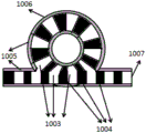
本发明提供的一种带有闭环波导结构的周期性极化晶体波导器件1000,如图1和图2所示,包括波导层1001和衬底1002,波导层1001位于衬底1002表面上。A periodically polarized
其中,波导层1001包含闭环波导1006和耦合波导1007,所述耦合波导1007和闭环波导1006可以相交,或者,所述耦合波导1007和闭环波导1006不相交,两者最近边缘间距小于1um。Wherein, the
耦合波导1007为开环结构。耦合波导1007可以是直波导,也可以是其他开环结构。The
耦合波导1007可以为一个或多个。当耦合波导1007为多个时,多个耦合波导1007可以采用不同的开环结构或者相同的开环结构。There can be one or
闭环波导1006为闭环结构。闭环波导1006可以是圆环、椭圆环、方形环、多边形等闭环结构。The closed-
闭环波导1006可以为一个或多个。当闭环波导1006为多个时,多个闭环波导1006可以采用不同的闭环结构或者相同的闭环结构。There can be one or more closed-
闭环波导1006的任何一部分的曲率半径至少大于周期性极化晶体波导器件1000的最大宽度的10倍。The radius of curvature of any portion of the
所述耦合波导1007和闭环波导1006可以是脊波导,也可以是掩埋波导。The
波导层1001还可以包括外包层1005,外包层1005设置在耦合波导1007和闭环波导1006的外表面。当然,耦合波导1007和闭环波导1006也可以直接裸露空气中,不使用外包层1005。The
外包层1005可以是与晶体材料不同的其他介质材料,如SiO2。The
进一步地,耦合波导1007和闭环波导1006均包括极化方向相反的第一区域1003和第二区域1004,第一区域1003和第二区域1004在耦合波导1007和闭环波导1006中均间隔设置,且第一区域1003和第二区域1004以一定规律周期排列,在耦合波导1007和闭环波导1006中形成周期性极化结构。当耦合波导1007和闭环波导1006相交时,耦合波导1007的第一区域1003和第二区域1004与闭环波导1006的第一区域1003和第二区域1004分别对应接触,如图2所示。Further, both the
所述耦合波导1007和闭环波导1006内晶体的极化周期分别是等占空比、啁啾、取样等类型;耦合波导1007和闭环波导1006内晶体的极化周期类型可以不相同,也可以相同。The polarization periods of the crystals in the
周期性极化晶体为非线性晶体,可以选取MgO:LiNbO3晶体为晶体材料,制得MgO:PPLN波导。MgO:PPLN波导的MgO:PPLN波导层1001的宽度为7~100μm,高度为5~100μm。Periodically polarized crystals are nonlinear crystals, and MgO:LiNbO 3 crystals can be selected as crystal materials to prepare MgO:PPLN waveguides. The MgO:
周期性极化晶体还可以选取KDP、BBO、LBO、KTA、KTP、LBGO、单轴有机材料、ZGP等作为极化基质材料。Periodically polarized crystals can also choose KDP, BBO, LBO, KTA, KTP, LBGO, uniaxial organic materials, ZGP, etc. as polarized matrix materials.
其中,所述耦合波导1007和闭环波导1006采用脊波导时,以周期性极化晶体为MgO:LiNbO3晶体为例,本发明实施例提出的带有闭环波导结构的周期性极化晶体波导器件1000的制备方法包括:Wherein, when the
选取MgO:LiNbO3晶体作为衬底1002;Select MgO:LiNbO 3 crystal as the
光刻后,室温下使用外加电场极化法对衬底1002进行周期极化,实现第一区域1003和第二区域1004极化方向周期反转结构的制备;After photolithography, the
再沉积一层NiCr合金的金属薄膜作为掩模层,通过光刻法将波导结构图形转移至衬底1002上,用湿法腐蚀后结合电感耦合等离子体(ICP)刻蚀的方法在衬底1002上刻蚀出包含闭环波导1006和耦合波导1007的脊形波导层1001;Then deposit a layer of NiCr alloy metal thin film as a mask layer, transfer the waveguide structure pattern to the
再沉积一层金属加介质掩膜,之后用化学溶剂将光刻胶和NiCr合金金属掩模层去除掉,再进行扩散或退火质子交换(APE),用化学溶剂去掉金属加介质掩膜,沉积外包层1005(也可省略),即制得带有闭环波导结构的周期性极化晶体波导器件1000。Deposit a layer of metal plus dielectric mask, then remove the photoresist and NiCr alloy metal mask layer with chemical solvent, then perform diffusion or annealing proton exchange (APE), remove the metal plus dielectric mask with chemical solvent, and deposit The outer cladding layer 1005 (can also be omitted), that is, the periodically polarized
所述耦合波导1007和闭环波导1006采用掩埋波导时,以周期性极化晶体为MgO:LiNbO3晶体为例,本发明实施例提出的带有闭环波导结构的周期性极化晶体波导器件1000的制备方法包括:When the
选取MgO:LixH1-xNbO3晶体作为衬底1002;Select MgO:Li x H 1-x NbO 3 crystal as the
光刻后,室温下使用外加电场极化法对衬底1002进行周期极化,实现第一区域1003和第二区域1004极化方向周期反转结构的制备;After photolithography, the
再沉积一层NiCr合金的金属薄膜作为掩模层,通过光刻法将波导结构图形转移至衬底1002上,然后进行退火反质子交换,后用化学溶剂将光刻胶和NiCr合金金属掩模层去除掉,沉积外包层1005(也可省略),即制得带有闭环波导结构的周期性极化晶体波导器件1000。Deposit a layer of NiCr alloy metal thin film as a mask layer, transfer the waveguide structure pattern to the
采用本发明实施例提出的带有闭环波导结构的周期性极化晶体波导器件1000的激光器,可以利用频率上转换(和频、倍频)和频率下转换(差频)、参量放大(OPA)和参量振荡(OPO)过程产生激光。所述产生的激光可以是连续激光,也可以是脉冲激光。所述激光器可以是外腔激光器,也可以是内腔激光器。所述激光器可以是单谐振激光器,也可以是双谐振激光器。The laser using the periodically polarized
下面结合具体实施例,对采用本发明实施例提出的带有闭环波导结构的周期性极化晶体波导器件1000的激光器进行示例性描述。其中所采用的“前”、“后”、“之间”等术语是相对于光路而言。The laser using the periodically poled
实施例1:Example 1:
在本实施例中,激光器采用内腔OPO结构,如图3所示。所述激光器包括:半导体激光器泵源2001、两个平凸透镜2002和2003组成的耦合透镜组、激光晶体2004、凸透镜2005、中间反射镜2006、带有闭环波导结构的MgO:PPLN波导2007、输出镜2008和反射镜2009。中间反射镜2006、输出镜2008和反射镜2009构成OPO腔。半导体激光器泵源2001、两个平凸透镜2002和2003组成的耦合透镜组、激光晶体2004、凸透镜2005、中间反射镜2006、带有闭环波导结构的MgO:PPLN波导2007和输出镜2008沿光路依次设置,反射镜2009位于中间反射镜2006的反射光路上。In this embodiment, the laser adopts an intracavity OPO structure, as shown in FIG. 3 . The laser includes: a semiconductor
其中,半导体激光器泵源2001的波长为808nm,光纤耦合输出激光束径为100~240μm。Wherein, the wavelength of the semiconductor
耦合透镜组将半导体激光器泵源2001光纤耦合输出的激光束聚焦到激光晶体2004前端面。平凸透镜2002和2003的焦距为15~45mm。The coupling lens group focuses the laser beam coupled by the semiconductor
激光晶体2004位于耦合透镜组和凸透镜2005之间。激光晶体2004为尺寸3×3×10mm3,掺杂浓度0.3~0.5at.%的a切Nd:YVO4晶体。激光晶体2004的前端面镀有808nm的增透膜和1064nm的高反膜,作为基频光的高反腔镜;后端面镀有808nm和1064nm的增透膜。在实验过程中Nd:YVO4晶体的温度恒定控制在20℃。The
凸透镜2005对激光晶体2004后端面输出的光进行处理,实现抽运光与振荡光的模式匹配。凸透镜2005的焦距为90~120mm。The
中间反射镜2006位于凸透镜2005和带有闭环波导结构的MgO:PPLN波导2007之间。中间反射镜2006双面镀有1064nm的增透膜,中间反射镜2006右端面镀有信号光和闲频光的高反射膜,反射率R>99.5%。The
带有闭环波导结构的MgO:PPLN波导2007位于中间反射镜2006和输出镜2008之间。因为MgO:PPLN晶体相比于普通的PPLN晶体具有更好的抗光折射能力,更高的光损伤阈值和更大的二阶非线性光学系数(d33),OPO腔中的MgO:PPLN晶体大小为1×10×40mm3,脊形波导宽度为7~100μm,高度为5~100μm;周期分别为29~32μm,并且前后端面镀有1064nm的增透膜,实验过程中通过将MgO:PPLN晶体放进控温炉来调节控制晶体的温度,温控炉温度调节范围为50~190℃,控制精度高于±0.3℃。A MgO:
输出镜2008用于输出激光。输出镜2008是曲率半径为90~120mm的凹透镜,输出镜2008凹面镀有1064nm和信号光的高反膜,反射率R>99.5%,同时镀闲频光的高透膜,透过率>90%。The
反射镜2009用于对信号光和闲频光进行反射。反射镜2009为曲率半径为90~120mm的平凹透镜,凹面同时镀有信号光和闲频光的高反膜,反射率>99.5%。The
实施例2Example 2
在本实施例中,激光器采用直腔内腔OPO结构,如图4所示。所述激光器包括:半导体激光器泵源3001、两个平凸透镜3002和3003组成的耦合透镜组、激光晶体3004、凸透镜3005、中间片3006、带有闭环波导结构的MgO:PPLN波导3007、输出片3008、第一分光片3010和第二分光片3009。中间片3006和输出片3008构成OPO腔。半导体激光器泵源3001、耦合透镜组、激光晶体3004、凸透镜3005、中间片3006、带有闭环波导结构的MgO:PPLN波导3007、输出片3008和第一分光片3010沿光路依次设置,第二分光片3009设置在第一分光片3010的反射光路上。In this embodiment, the laser adopts a straight-cavity intra-cavity OPO structure, as shown in FIG. 4 . The laser includes: a semiconductor
其中,半导体激光器泵源的波长为808nm,光纤耦合输出激光束径为200μm。Among them, the wavelength of the pump source of the semiconductor laser is 808 nm, and the diameter of the fiber-coupled output laser beam is 200 μm.
耦合透镜组将光纤耦合输出的激光聚焦到激光晶体3004前端面。平凸透镜3002和3003的焦距为15~45mm。The coupling lens group focuses the laser light coupled out by the fiber to the front face of the
激光晶体3004位于耦合透镜组和激光晶体3004之间。激光晶体3004为尺寸3×3×10mm3,掺杂浓度0.3~0.5at.%的a切Nd:YVO4晶体。激光晶体3004的前端面镀有808nm的增透膜和1064nm的高反膜,作为基频光的高反腔镜;后端面镀有808nm和1064nm的增透膜。在实验过程中Nd:YVO4晶体3004温度恒定控制在20℃。The
凸透镜3005对激光晶体3004后端面输出的光进行处理,改变抽运光的束径大小。凸透镜3005的焦距为90~120mm。The
中间片3006位于为凸透镜3005和带有闭环波导结构的MgO:PPLN波导3007之间。中间片3006为平片,双面镀有1064nm的增透膜,同时右端面镀信号光(1450~1650nm)和闲频光(3000~4000nm)的高反膜,反射率R>99.9%。The
带有闭环波导结构的MgO:PPLN波导3007,因为MgO:PPLN晶体相比于普通的PPLN晶体具有更好的抗光折射能力,更高的光损伤阈值和更大的二阶非线性光学系数(d33),OPO腔中的MgO:PPLN晶体大小为1×10×40mm3,脊形波导宽度为7~100μm,高度为5~100μm;周期分别为29~32μm,并且前后端面镀有1064nm的增透膜。实验过程中通过将MgO:PPLN晶体放进控温炉来调节控制晶体的温度,温控炉温度调节范围为50~190℃,控制精度高于±0.3℃。为便于光路调整,控温炉固定在多维调整平台上。MgO:
输出镜3008为曲率半径为400~550mm的平凹透镜,凹面镀1064nm高反膜(反射率R>99.5%)、信号光的部分反射膜(R=93~95%)和闲频光高透膜(透过率>90%)。The
Nd:YVO4晶体3004的前端面到输出镜3008构成抽运光(1064nm)的谐振腔,腔长为125mm。The front end of the Nd:
中间片3006和输出片3008构成OPO腔,腔长为70mm。The
第一分光片3010对闲频光高透(透过率>90%)、信号光高反(R>99.9%)和泵浦光1064nm高反(R>99.9%),第一分光片3010透过的光为激光器输出的闲频光3012。The
第二分光片3009对泵浦光高透透过率>90%,信号光高反,反射率R>99.9%,第二分光片3009反射的光为激光器输出的信号光3011,第二分光片3009透过的光为激光器输出的泵浦光3013。The
实施例3Example 3
在本实施例中,激光器采用结构简单紧凑的直线腔设计。本实施例的激光二极管抽运Cr4+:YAG/PPLN调Q绿光脉冲激光器的结构示意图如图5所示,包括:沿光路依次设置的抽运源4001、透镜4002和4003组成的耦合透镜组、Nd:YVO4晶体4004、Cr4+:YAG晶体4005和带有闭环波导结构的MgO:PPLN波导4006。In this embodiment, the laser adopts a linear cavity design with a simple and compact structure. The structural representation of the laser diode pumped Cr 4+ of the present embodiment: YAG/PPLN Q-switched green pulsed laser is shown in Figure 5, including: a
抽运源4001为光纤耦合输出的半导体激光器(LD),为了让半导体激光器的发射波段与激活离子的吸收峰更好地吻合,通过控制半导体激光器的温度,让其发射波长稳定在808nm左右。抽运源4001输出尾纤的光纤芯径是100~400um,数值孔径(NA)是0.22,最大输出功率是20W。The
透镜4002和4003的聚焦比例为1:1。耦合透镜组将抽运光束准直聚焦到Nd:YVO4晶体4004上,聚焦后光斑半径约为50~200um。The focusing ratio of
本实施例中采用的Nd:YVO4晶体4004中Nd3+的掺杂原子数分数为0.4~0.6%,尺寸为3×3×6mm3,左端面键808nm增透、1064nm高反的双色膜,右端面镀808nm增透、1064nm増透的双色膜。为了对晶体进行高效控温,用铟箔包裹晶体镶嵌于紫铜块内,并通过水冷系统对紫铜块进行控温,使晶体表面温度维持在25℃左右。In the Nd:YVO 4 crystal 4004 used in this example, the doped atomic fraction of Nd 3+ is 0.4-0.6%, the size is 3×3×6mm 3 , and the double-color film with 808nm antireflection and 1064nm high reflection on the left end face , the right end surface is coated with 808nm anti-reflection and 1064nm anti-reflection two-color film. In order to efficiently control the temperature of the crystal, the crystal is wrapped with indium foil and embedded in a copper block, and the temperature of the copper block is controlled by a water cooling system to maintain the surface temperature of the crystal at about 25°C.
Cr4+:YAG晶体4005位于Nd:YVO4晶体4004光路后方。Cr4+:YAG晶体4005的尺寸为3×3×1mm3,初始透过率为90%,两面均镀808nm增透、1064nm增透的双色膜。Cr 4+ :
MgO:PPLN波导4006的大小为1×10×40mm3,脊形波导宽度为7~100μm,高度为5~100μm;周期分别为4~15μm,入光面镀1064nm的増透膜、532nm的激光反射膜,出光面镀1064nm的激光反射膜、532nm的增透膜,利用TEC温度控制器单独对PPLN晶体进行控温,温度控制范围是-20℃~60℃,控制精度为±0.1℃。The size of the MgO:
在连续绿光工作在最佳模式下,将Cr4+:YAG晶体4005插入激光谐振腔内,并靠近MgO:PPLN晶体4006放置。当激光谐振腔的腔长设置为40mm,Nd:YVO4晶体4004吸收功率为2.7W时,微调Cr4+:YAG晶体4005和MgO:PPLN波导4006的位置可以得到532nm脉冲绿光4007输出。When the continuous green light works in the best mode, insert the Cr 4+ :
以上,对本发明的实施方式进行了说明。但是,本发明不限定于上述实施方式。凡在本发明的精神和原则之内,所做的任何修改、等同替换、改进等,均应包含在本发明的保护范围之内。The embodiments of the present invention have been described above. However, the present invention is not limited to the above-mentioned embodiments. Any modifications, equivalent replacements, improvements, etc. made within the spirit and principles of the present invention shall be included within the protection scope of the present invention.
Claims (10)
Priority Applications (1)
| Application Number | Priority Date | Filing Date | Title |
|---|---|---|---|
| CN201810732310.0A CN108683071B (en) | 2018-07-05 | 2018-07-05 | Periodically Polarized Crystal Waveguide Device and Laser with Closed-loop Waveguide Structure |
Applications Claiming Priority (1)
| Application Number | Priority Date | Filing Date | Title |
|---|---|---|---|
| CN201810732310.0A CN108683071B (en) | 2018-07-05 | 2018-07-05 | Periodically Polarized Crystal Waveguide Device and Laser with Closed-loop Waveguide Structure |
Publications (2)
| Publication Number | Publication Date |
|---|---|
| CN108683071A CN108683071A (en) | 2018-10-19 |
| CN108683071B true CN108683071B (en) | 2023-06-09 |
Family
ID=63813425
Family Applications (1)
| Application Number | Title | Priority Date | Filing Date |
|---|---|---|---|
| CN201810732310.0A Active CN108683071B (en) | 2018-07-05 | 2018-07-05 | Periodically Polarized Crystal Waveguide Device and Laser with Closed-loop Waveguide Structure |
Country Status (1)
| Country | Link |
|---|---|
| CN (1) | CN108683071B (en) |
Citations (6)
| Publication number | Priority date | Publication date | Assignee | Title |
|---|---|---|---|---|
| CN1747260A (en) * | 2005-07-15 | 2006-03-15 | 天津大学 | A device for generating terahertz from a non-periodically polarized crystal dual-wavelength optical parametric oscillator |
| CN102891427A (en) * | 2012-10-16 | 2013-01-23 | 中国科学院上海光学精密机械研究所 | Small frequency multiplication visible light fiber laser |
| CN103956644A (en) * | 2014-05-16 | 2014-07-30 | 中国科学院福建物质结构研究所 | Continuous ultraviolet laser based on periodical polarization reversal crystal straight cavity |
| CN104466651A (en) * | 2014-12-02 | 2015-03-25 | 中国电子科技集团公司第四十一研究所 | Annular integrated laser frequency doubling device |
| EP2988096A1 (en) * | 2014-08-18 | 2016-02-24 | Honeywell International Inc. | Resonant fiber optic gyroscope with polarizing crystal waveguide coupler |
| CN106707656A (en) * | 2017-01-11 | 2017-05-24 | 深圳大学 | Periodic poling crystal and optical parameter amplifier |
Family Cites Families (3)
| Publication number | Priority date | Publication date | Assignee | Title |
|---|---|---|---|---|
| US6763042B2 (en) * | 2001-12-14 | 2004-07-13 | Evans & Sutherland Computer Corporation | Apparatus and method for frequency conversion and mixing of laser light |
| US20090245294A1 (en) * | 2007-07-31 | 2009-10-01 | Zecotek Laser Systems Pte. Ltd. | Fibre Laser with Intra-cavity Frequency Doubling |
| US20090231686A1 (en) * | 2008-01-12 | 2009-09-17 | Robert Atkins | Multi-functional integrated optical waveguides |
-
2018
- 2018-07-05 CN CN201810732310.0A patent/CN108683071B/en active Active
Patent Citations (6)
| Publication number | Priority date | Publication date | Assignee | Title |
|---|---|---|---|---|
| CN1747260A (en) * | 2005-07-15 | 2006-03-15 | 天津大学 | A device for generating terahertz from a non-periodically polarized crystal dual-wavelength optical parametric oscillator |
| CN102891427A (en) * | 2012-10-16 | 2013-01-23 | 中国科学院上海光学精密机械研究所 | Small frequency multiplication visible light fiber laser |
| CN103956644A (en) * | 2014-05-16 | 2014-07-30 | 中国科学院福建物质结构研究所 | Continuous ultraviolet laser based on periodical polarization reversal crystal straight cavity |
| EP2988096A1 (en) * | 2014-08-18 | 2016-02-24 | Honeywell International Inc. | Resonant fiber optic gyroscope with polarizing crystal waveguide coupler |
| CN104466651A (en) * | 2014-12-02 | 2015-03-25 | 中国电子科技集团公司第四十一研究所 | Annular integrated laser frequency doubling device |
| CN106707656A (en) * | 2017-01-11 | 2017-05-24 | 深圳大学 | Periodic poling crystal and optical parameter amplifier |
Also Published As
| Publication number | Publication date |
|---|---|
| CN108683071A (en) | 2018-10-19 |
Similar Documents
| Publication | Publication Date | Title |
|---|---|---|
| EP0788015A2 (en) | Multi quasi phase matched interactions in a non-linear crystal | |
| Iwai et al. | High-power blue generation from a periodically poled MgO: LiNbO 3 ridge-type waveguide by frequency doubling of a diode end-pumped Nd: Y 3 Al 5 O 12 laser | |
| Myers et al. | Quasi-phase-matched optical parametric oscillators in bulk periodically poled LiNbO3 | |
| EP3851912B1 (en) | Visible to ultraviolet band optical frequency converter | |
| KR102100728B1 (en) | Highly Efficient, Single-Pass, Harmonic Generator with Round Output Beam | |
| CN104779516B (en) | In infrared single-frequency optical parametric oscillator | |
| US8184667B2 (en) | Electro-optic Bragg deflector and method of using it as laser Q-switch in an actively Q-switched laser and an actively Q-switched wavelength-conversion laser | |
| US20240353735A1 (en) | Single-frequency continuous-wave optical parametric oscillator | |
| JP2011511950A (en) | Ferroelectric domain inversion method and its application | |
| CN109149346B (en) | A Multi-optical Parametric Oscillator Realizing Intracavity Regulation of Energy Inverse Conversion | |
| WO1994024735A1 (en) | Optical parametric amplifiers and oscillators pumped by tunable laser sources | |
| Laurell | Periodically poled materials for miniature light sources | |
| Sun et al. | High energy and high efficiency 3.4 μ m extracavity KTA optical parametric oscillator | |
| CN109038201B (en) | A Multi-optical Parametric Oscillator with Active Control of Energy Group Distribution Ratio | |
| US20090059967A1 (en) | Electro-Optic Bragg Deflector and Method of Using It as Laser Q-Switch in a Q-Switched Laser and a Q-Switched Wavelength-Conversion Laser | |
| Tohmon et al. | Blue light source using guided-wave frequency doubler with a diode laser | |
| CN108683071B (en) | Periodically Polarized Crystal Waveguide Device and Laser with Closed-loop Waveguide Structure | |
| Zhu et al. | Electro-optic Q-switched intracavity optical parametric oscillator at 1.53 μm based on KTiOAsO4 | |
| CN208580946U (en) | Periodic polarized crystal waveguide device and laser with closed loop waveguiding structure | |
| CN105006734B (en) | A kind of 2 μm of lasers that half Intracavity OPO is formed based on body grating | |
| JP2718259B2 (en) | Short wavelength laser light source | |
| Fengqin et al. | High-power tunable single-frequency 461 nm generation from an intracavity doubled Ti: sapphire laser with PPKTP | |
| Mu et al. | Efficient KTiOPO 4 blue-light converter for monochromatic 1.3188-μm emission line of pulsed Nd: YAG laser | |
| Pasiskevicius et al. | Low-threshold midinfrared optical parametric oscillation in periodically poled KTiOPO4 | |
| Sheng et al. | A continuous-wave tunable orange-red source based on sum-frequency generation in an intra-cavity periodically poled LiNbO3 singly resonant optical parametric oscillator cavity |
Legal Events
| Date | Code | Title | Description |
|---|---|---|---|
| PB01 | Publication | ||
| PB01 | Publication | ||
| SE01 | Entry into force of request for substantive examination | ||
| SE01 | Entry into force of request for substantive examination | ||
| GR01 | Patent grant | ||
| GR01 | Patent grant |